EP1558449B1 - Method for producing tamper-proof identification elements - Google Patents
Method for producing tamper-proof identification elements Download PDFInfo
- Publication number
- EP1558449B1 EP1558449B1 EP03784094.9A EP03784094A EP1558449B1 EP 1558449 B1 EP1558449 B1 EP 1558449B1 EP 03784094 A EP03784094 A EP 03784094A EP 1558449 B1 EP1558449 B1 EP 1558449B1
- Authority
- EP
- European Patent Office
- Prior art keywords
- layer
- printing
- optically transparent
- spacer layer
- metallic clusters
- Prior art date
- Legal status (The legal status is an assumption and is not a legal conclusion. Google has not performed a legal analysis and makes no representation as to the accuracy of the status listed.)
- Expired - Lifetime
Links
- 238000004519 manufacturing process Methods 0.000 title claims description 13
- 239000010410 layer Substances 0.000 claims description 164
- 239000000758 substrate Substances 0.000 claims description 45
- 238000000034 method Methods 0.000 claims description 42
- 238000007639 printing Methods 0.000 claims description 29
- 125000006850 spacer group Chemical group 0.000 claims description 23
- 229920000642 polymer Polymers 0.000 claims description 13
- 230000008569 process Effects 0.000 claims description 13
- 230000000694 effects Effects 0.000 claims description 12
- 238000004544 sputter deposition Methods 0.000 claims description 10
- 239000002904 solvent Substances 0.000 claims description 9
- 238000005516 engineering process Methods 0.000 claims description 7
- 239000000126 substance Substances 0.000 claims description 7
- 238000005507 spraying Methods 0.000 claims description 6
- 238000007646 gravure printing Methods 0.000 claims description 5
- 238000010422 painting Methods 0.000 claims description 5
- 238000005266 casting Methods 0.000 claims description 4
- 238000007650 screen-printing Methods 0.000 claims description 4
- 238000005240 physical vapour deposition Methods 0.000 claims description 3
- 238000009736 wetting Methods 0.000 claims description 3
- 238000005304 joining Methods 0.000 claims description 2
- 239000007788 liquid Substances 0.000 claims description 2
- 230000001590 oxidative effect Effects 0.000 claims description 2
- 239000011241 protective layer Substances 0.000 claims description 2
- 238000000151 deposition Methods 0.000 claims 3
- 230000008021 deposition Effects 0.000 claims 3
- 239000005708 Sodium hypochlorite Substances 0.000 claims 1
- 239000004920 heat-sealing lacquer Substances 0.000 claims 1
- SUKJFIGYRHOWBL-UHFFFAOYSA-N sodium hypochlorite Chemical compound [Na+].Cl[O-] SUKJFIGYRHOWBL-UHFFFAOYSA-N 0.000 claims 1
- 239000003973 paint Substances 0.000 description 17
- 239000000049 pigment Substances 0.000 description 16
- 229910052751 metal Inorganic materials 0.000 description 14
- 239000002184 metal Substances 0.000 description 14
- PXHVJJICTQNCMI-UHFFFAOYSA-N nickel Substances [Ni] PXHVJJICTQNCMI-UHFFFAOYSA-N 0.000 description 10
- 239000010949 copper Substances 0.000 description 9
- 239000013047 polymeric layer Substances 0.000 description 9
- 239000000853 adhesive Substances 0.000 description 8
- 230000001070 adhesive effect Effects 0.000 description 8
- 229910052782 aluminium Inorganic materials 0.000 description 8
- 230000003287 optical effect Effects 0.000 description 8
- -1 MOPP Substances 0.000 description 7
- 229910052802 copper Inorganic materials 0.000 description 7
- 239000000203 mixture Substances 0.000 description 7
- 239000000020 Nitrocellulose Substances 0.000 description 6
- XAGFODPZIPBFFR-UHFFFAOYSA-N aluminium Chemical compound [Al] XAGFODPZIPBFFR-UHFFFAOYSA-N 0.000 description 6
- 229910052804 chromium Inorganic materials 0.000 description 6
- 239000011651 chromium Substances 0.000 description 6
- 229920001220 nitrocellulos Polymers 0.000 description 6
- 238000001228 spectrum Methods 0.000 description 6
- XLYOFNOQVPJJNP-UHFFFAOYSA-N water Substances O XLYOFNOQVPJJNP-UHFFFAOYSA-N 0.000 description 6
- RYGMFSIKBFXOCR-UHFFFAOYSA-N Copper Chemical compound [Cu] RYGMFSIKBFXOCR-UHFFFAOYSA-N 0.000 description 5
- 239000000975 dye Substances 0.000 description 5
- PCHJSUWPFVWCPO-UHFFFAOYSA-N gold Chemical compound [Au] PCHJSUWPFVWCPO-UHFFFAOYSA-N 0.000 description 5
- 239000010931 gold Substances 0.000 description 5
- XEEYBQQBJWHFJM-UHFFFAOYSA-N iron Substances [Fe] XEEYBQQBJWHFJM-UHFFFAOYSA-N 0.000 description 5
- 239000004922 lacquer Substances 0.000 description 5
- 238000010030 laminating Methods 0.000 description 5
- 239000002346 layers by function Substances 0.000 description 5
- 230000005291 magnetic effect Effects 0.000 description 5
- 229910052759 nickel Inorganic materials 0.000 description 5
- VYZAMTAEIAYCRO-UHFFFAOYSA-N Chromium Chemical compound [Cr] VYZAMTAEIAYCRO-UHFFFAOYSA-N 0.000 description 4
- 238000010521 absorption reaction Methods 0.000 description 4
- 238000000576 coating method Methods 0.000 description 4
- 239000003086 colorant Substances 0.000 description 4
- 150000001875 compounds Chemical class 0.000 description 4
- 239000012153 distilled water Substances 0.000 description 4
- 239000011888 foil Substances 0.000 description 4
- 229910052737 gold Inorganic materials 0.000 description 4
- BASFCYQUMIYNBI-UHFFFAOYSA-N platinum Chemical compound [Pt] BASFCYQUMIYNBI-UHFFFAOYSA-N 0.000 description 4
- 239000004800 polyvinyl chloride Substances 0.000 description 4
- 229920000915 polyvinyl chloride Polymers 0.000 description 4
- 229910052709 silver Inorganic materials 0.000 description 4
- JOYRKODLDBILNP-UHFFFAOYSA-N Ethyl urethane Chemical compound CCOC(N)=O JOYRKODLDBILNP-UHFFFAOYSA-N 0.000 description 3
- KDLHZDBZIXYQEI-UHFFFAOYSA-N Palladium Chemical compound [Pd] KDLHZDBZIXYQEI-UHFFFAOYSA-N 0.000 description 3
- 239000004372 Polyvinyl alcohol Substances 0.000 description 3
- BQCADISMDOOEFD-UHFFFAOYSA-N Silver Chemical compound [Ag] BQCADISMDOOEFD-UHFFFAOYSA-N 0.000 description 3
- 239000000654 additive Substances 0.000 description 3
- 239000011248 coating agent Substances 0.000 description 3
- 239000002131 composite material Substances 0.000 description 3
- 230000001419 dependent effect Effects 0.000 description 3
- 229910052742 iron Inorganic materials 0.000 description 3
- 239000003550 marker Substances 0.000 description 3
- 229910001092 metal group alloy Inorganic materials 0.000 description 3
- 238000001465 metallisation Methods 0.000 description 3
- 150000002739 metals Chemical class 0.000 description 3
- 229920003023 plastic Polymers 0.000 description 3
- 239000004033 plastic Substances 0.000 description 3
- 229920000728 polyester Polymers 0.000 description 3
- 229920002451 polyvinyl alcohol Polymers 0.000 description 3
- 239000000047 product Substances 0.000 description 3
- 238000007761 roller coating Methods 0.000 description 3
- 150000003839 salts Chemical class 0.000 description 3
- 239000004332 silver Substances 0.000 description 3
- 230000003595 spectral effect Effects 0.000 description 3
- RSWGJHLUYNHPMX-UHFFFAOYSA-N Abietic-Saeure Natural products C12CCC(C(C)C)=CC2=CCC2C1(C)CCCC2(C)C(O)=O RSWGJHLUYNHPMX-UHFFFAOYSA-N 0.000 description 2
- NIXOWILDQLNWCW-UHFFFAOYSA-M Acrylate Chemical compound [O-]C(=O)C=C NIXOWILDQLNWCW-UHFFFAOYSA-M 0.000 description 2
- 239000005995 Aluminium silicate Substances 0.000 description 2
- 241000167854 Bourreria succulenta Species 0.000 description 2
- 108091003079 Bovine Serum Albumin Proteins 0.000 description 2
- 239000004593 Epoxy Substances 0.000 description 2
- 229920000877 Melamine resin Polymers 0.000 description 2
- 239000004698 Polyethylene Substances 0.000 description 2
- 239000004743 Polypropylene Substances 0.000 description 2
- KHPCPRHQVVSZAH-HUOMCSJISA-N Rosin Natural products O(C/C=C/c1ccccc1)[C@H]1[C@H](O)[C@@H](O)[C@@H](O)[C@@H](CO)O1 KHPCPRHQVVSZAH-HUOMCSJISA-N 0.000 description 2
- CDBYLPFSWZWCQE-UHFFFAOYSA-L Sodium Carbonate Chemical compound [Na+].[Na+].[O-]C([O-])=O CDBYLPFSWZWCQE-UHFFFAOYSA-L 0.000 description 2
- 229910010413 TiO 2 Inorganic materials 0.000 description 2
- GWEVSGVZZGPLCZ-UHFFFAOYSA-N Titan oxide Chemical compound O=[Ti]=O GWEVSGVZZGPLCZ-UHFFFAOYSA-N 0.000 description 2
- 239000002318 adhesion promoter Substances 0.000 description 2
- 229920000180 alkyd Polymers 0.000 description 2
- 229910045601 alloy Inorganic materials 0.000 description 2
- 239000000956 alloy Substances 0.000 description 2
- 235000012211 aluminium silicate Nutrition 0.000 description 2
- 239000011230 binding agent Substances 0.000 description 2
- 230000005540 biological transmission Effects 0.000 description 2
- 230000015572 biosynthetic process Effects 0.000 description 2
- 229940098773 bovine serum albumin Drugs 0.000 description 2
- 230000008859 change Effects 0.000 description 2
- 235000019693 cherries Nutrition 0.000 description 2
- UOUJSJZBMCDAEU-UHFFFAOYSA-N chromium(3+);oxygen(2-) Chemical class [O-2].[O-2].[O-2].[Cr+3].[Cr+3] UOUJSJZBMCDAEU-UHFFFAOYSA-N 0.000 description 2
- 238000004043 dyeing Methods 0.000 description 2
- 238000010894 electron beam technology Methods 0.000 description 2
- 238000005530 etching Methods 0.000 description 2
- 150000002343 gold Chemical class 0.000 description 2
- WQYVRQLZKVEZGA-UHFFFAOYSA-N hypochlorite Chemical compound Cl[O-] WQYVRQLZKVEZGA-UHFFFAOYSA-N 0.000 description 2
- 239000000976 ink Substances 0.000 description 2
- 239000012212 insulator Substances 0.000 description 2
- 230000003993 interaction Effects 0.000 description 2
- 238000010884 ion-beam technique Methods 0.000 description 2
- 239000012948 isocyanate Substances 0.000 description 2
- 150000002513 isocyanates Chemical class 0.000 description 2
- NLYAJNPCOHFWQQ-UHFFFAOYSA-N kaolin Chemical compound O.O.O=[Al]O[Si](=O)O[Si](=O)O[Al]=O NLYAJNPCOHFWQQ-UHFFFAOYSA-N 0.000 description 2
- 238000003475 lamination Methods 0.000 description 2
- 239000000463 material Substances 0.000 description 2
- JDSHMPZPIAZGSV-UHFFFAOYSA-N melamine Chemical compound NC1=NC(N)=NC(N)=N1 JDSHMPZPIAZGSV-UHFFFAOYSA-N 0.000 description 2
- 229910044991 metal oxide Inorganic materials 0.000 description 2
- 150000004706 metal oxides Chemical class 0.000 description 2
- 238000012986 modification Methods 0.000 description 2
- 230000004048 modification Effects 0.000 description 2
- 230000007935 neutral effect Effects 0.000 description 2
- 229910052763 palladium Inorganic materials 0.000 description 2
- 229910052697 platinum Inorganic materials 0.000 description 2
- 239000004417 polycarbonate Substances 0.000 description 2
- 229920000139 polyethylene terephthalate Polymers 0.000 description 2
- 239000005020 polyethylene terephthalate Substances 0.000 description 2
- 230000005855 radiation Effects 0.000 description 2
- 239000000523 sample Substances 0.000 description 2
- 238000003756 stirring Methods 0.000 description 2
- 150000004763 sulfides Chemical class 0.000 description 2
- 238000003786 synthesis reaction Methods 0.000 description 2
- 239000011135 tin Substances 0.000 description 2
- 229910052718 tin Inorganic materials 0.000 description 2
- KHPCPRHQVVSZAH-UHFFFAOYSA-N trans-cinnamyl beta-D-glucopyranoside Natural products OC1C(O)C(O)C(CO)OC1OCC=CC1=CC=CC=C1 KHPCPRHQVVSZAH-UHFFFAOYSA-N 0.000 description 2
- 238000012546 transfer Methods 0.000 description 2
- 238000007740 vapor deposition Methods 0.000 description 2
- 239000002966 varnish Substances 0.000 description 2
- 238000012800 visualization Methods 0.000 description 2
- 238000007704 wet chemistry method Methods 0.000 description 2
- 229910052984 zinc sulfide Inorganic materials 0.000 description 2
- OKTJSMMVPCPJKN-UHFFFAOYSA-N Carbon Chemical compound [C] OKTJSMMVPCPJKN-UHFFFAOYSA-N 0.000 description 1
- 206010013710 Drug interaction Diseases 0.000 description 1
- LFQSCWFLJHTTHZ-UHFFFAOYSA-N Ethanol Chemical compound CCO LFQSCWFLJHTTHZ-UHFFFAOYSA-N 0.000 description 1
- MURCDOXDAHPNRQ-ZJKZPDEISA-N L-685,458 Chemical compound C([C@@H]([C@H](O)C[C@H](C(=O)N[C@@H](CC(C)C)C(=O)N[C@@H](CC=1C=CC=CC=1)C(N)=O)CC=1C=CC=CC=1)NC(=O)OC(C)(C)C)C1=CC=CC=C1 MURCDOXDAHPNRQ-ZJKZPDEISA-N 0.000 description 1
- 239000004696 Poly ether ether ketone Substances 0.000 description 1
- 239000004734 Polyphenylene sulfide Substances 0.000 description 1
- XUIMIQQOPSSXEZ-UHFFFAOYSA-N Silicon Chemical compound [Si] XUIMIQQOPSSXEZ-UHFFFAOYSA-N 0.000 description 1
- ATJFFYVFTNAWJD-UHFFFAOYSA-N Tin Chemical compound [Sn] ATJFFYVFTNAWJD-UHFFFAOYSA-N 0.000 description 1
- 239000005083 Zinc sulfide Substances 0.000 description 1
- 230000002745 absorbent Effects 0.000 description 1
- 239000002250 absorbent Substances 0.000 description 1
- 239000006096 absorbing agent Substances 0.000 description 1
- 230000009471 action Effects 0.000 description 1
- 230000000996 additive effect Effects 0.000 description 1
- 239000012790 adhesive layer Substances 0.000 description 1
- JRBRVDCKNXZZGH-UHFFFAOYSA-N alumane;copper Chemical compound [AlH3].[Cu] JRBRVDCKNXZZGH-UHFFFAOYSA-N 0.000 description 1
- 238000004458 analytical method Methods 0.000 description 1
- 229940051881 anilide analgesics and antipyretics Drugs 0.000 description 1
- 150000003931 anilides Chemical class 0.000 description 1
- GHPGOEFPKIHBNM-UHFFFAOYSA-N antimony(3+);oxygen(2-) Chemical compound [O-2].[O-2].[O-2].[Sb+3].[Sb+3] GHPGOEFPKIHBNM-UHFFFAOYSA-N 0.000 description 1
- 238000013459 approach Methods 0.000 description 1
- 239000000987 azo dye Substances 0.000 description 1
- JUPQTSLXMOCDHR-UHFFFAOYSA-N benzene-1,4-diol;bis(4-fluorophenyl)methanone Chemical compound OC1=CC=C(O)C=C1.C1=CC(F)=CC=C1C(=O)C1=CC=C(F)C=C1 JUPQTSLXMOCDHR-UHFFFAOYSA-N 0.000 description 1
- 230000001680 brushing effect Effects 0.000 description 1
- 239000006229 carbon black Substances 0.000 description 1
- 239000000969 carrier Substances 0.000 description 1
- 239000012876 carrier material Substances 0.000 description 1
- 229920002678 cellulose Polymers 0.000 description 1
- 239000001913 cellulose Substances 0.000 description 1
- 238000005119 centrifugation Methods 0.000 description 1
- 229910017052 cobalt Inorganic materials 0.000 description 1
- 239000010941 cobalt Substances 0.000 description 1
- GUTLYIVDDKVIGB-UHFFFAOYSA-N cobalt atom Chemical compound [Co] GUTLYIVDDKVIGB-UHFFFAOYSA-N 0.000 description 1
- 239000000084 colloidal system Substances 0.000 description 1
- 238000009833 condensation Methods 0.000 description 1
- 230000005494 condensation Effects 0.000 description 1
- 239000002482 conductive additive Substances 0.000 description 1
- 238000007796 conventional method Methods 0.000 description 1
- TVZPLCNGKSPOJA-UHFFFAOYSA-N copper zinc Chemical compound [Cu].[Zn] TVZPLCNGKSPOJA-UHFFFAOYSA-N 0.000 description 1
- 238000003851 corona treatment Methods 0.000 description 1
- 239000011222 crystalline ceramic Substances 0.000 description 1
- 229910002106 crystalline ceramic Inorganic materials 0.000 description 1
- 238000001212 derivatisation Methods 0.000 description 1
- 230000005292 diamagnetic effect Effects 0.000 description 1
- 238000009826 distribution Methods 0.000 description 1
- 238000001035 drying Methods 0.000 description 1
- 238000009713 electroplating Methods 0.000 description 1
- YQGOJNYOYNNSMM-UHFFFAOYSA-N eosin Chemical compound [Na+].OC(=O)C1=CC=CC=C1C1=C2C=C(Br)C(=O)C(Br)=C2OC2=C(Br)C(O)=C(Br)C=C21 YQGOJNYOYNNSMM-UHFFFAOYSA-N 0.000 description 1
- 150000002148 esters Chemical class 0.000 description 1
- 238000001704 evaporation Methods 0.000 description 1
- 230000008020 evaporation Effects 0.000 description 1
- 230000005294 ferromagnetic effect Effects 0.000 description 1
- 229920002457 flexible plastic Polymers 0.000 description 1
- 229910052732 germanium Inorganic materials 0.000 description 1
- GNPVGFCGXDBREM-UHFFFAOYSA-N germanium atom Chemical compound [Ge] GNPVGFCGXDBREM-UHFFFAOYSA-N 0.000 description 1
- 229910002804 graphite Inorganic materials 0.000 description 1
- 239000010439 graphite Substances 0.000 description 1
- 229910052736 halogen Inorganic materials 0.000 description 1
- 150000002367 halogens Chemical class 0.000 description 1
- 229920000592 inorganic polymer Polymers 0.000 description 1
- 239000010416 ion conductor Substances 0.000 description 1
- 239000004973 liquid crystal related substance Substances 0.000 description 1
- 229920002521 macromolecule Polymers 0.000 description 1
- 229910052976 metal sulfide Inorganic materials 0.000 description 1
- 229920000620 organic polymer Polymers 0.000 description 1
- 238000004806 packaging method and process Methods 0.000 description 1
- 230000005298 paramagnetic effect Effects 0.000 description 1
- 239000002245 particle Substances 0.000 description 1
- 238000009832 plasma treatment Methods 0.000 description 1
- 239000002985 plastic film Substances 0.000 description 1
- 229920001643 poly(ether ketone) Polymers 0.000 description 1
- 229920003229 poly(methyl methacrylate) Polymers 0.000 description 1
- 229920000058 polyacrylate Polymers 0.000 description 1
- 229920006260 polyaryletherketone Polymers 0.000 description 1
- 229920000515 polycarbonate Polymers 0.000 description 1
- 229920000647 polyepoxide Polymers 0.000 description 1
- 229920002530 polyetherether ketone Polymers 0.000 description 1
- 229920000573 polyethylene Polymers 0.000 description 1
- 239000004926 polymethyl methacrylate Substances 0.000 description 1
- 229920001155 polypropylene Polymers 0.000 description 1
- 229920001296 polysiloxane Polymers 0.000 description 1
- 239000004814 polyurethane Substances 0.000 description 1
- 229920002635 polyurethane Polymers 0.000 description 1
- 239000002244 precipitate Substances 0.000 description 1
- 238000012545 processing Methods 0.000 description 1
- 230000001681 protective effect Effects 0.000 description 1
- 238000003847 radiation curing Methods 0.000 description 1
- 239000011541 reaction mixture Substances 0.000 description 1
- 230000000717 retained effect Effects 0.000 description 1
- 230000003678 scratch resistant effect Effects 0.000 description 1
- 239000000565 sealant Substances 0.000 description 1
- 239000004065 semiconductor Substances 0.000 description 1
- 229910052710 silicon Inorganic materials 0.000 description 1
- 239000010703 silicon Substances 0.000 description 1
- LIVNPJMFVYWSIS-UHFFFAOYSA-N silicon monoxide Chemical class [Si-]#[O+] LIVNPJMFVYWSIS-UHFFFAOYSA-N 0.000 description 1
- 229910052814 silicon oxide Inorganic materials 0.000 description 1
- 239000010944 silver (metal) Substances 0.000 description 1
- 239000011734 sodium Substances 0.000 description 1
- 229910000029 sodium carbonate Inorganic materials 0.000 description 1
- 239000001509 sodium citrate Substances 0.000 description 1
- 238000001179 sorption measurement Methods 0.000 description 1
- 229910052950 sphalerite Inorganic materials 0.000 description 1
- 239000012798 spherical particle Substances 0.000 description 1
- 238000010186 staining Methods 0.000 description 1
- 229910001220 stainless steel Inorganic materials 0.000 description 1
- 239000010935 stainless steel Substances 0.000 description 1
- 239000004094 surface-active agent Substances 0.000 description 1
- 239000004753 textile Substances 0.000 description 1
- 238000007669 thermal treatment Methods 0.000 description 1
- 239000010936 titanium Substances 0.000 description 1
- 229910052719 titanium Inorganic materials 0.000 description 1
- 239000004408 titanium dioxide Substances 0.000 description 1
- 239000012780 transparent material Substances 0.000 description 1
- HRXKRNGNAMMEHJ-UHFFFAOYSA-K trisodium citrate Chemical compound [Na+].[Na+].[Na+].[O-]C(=O)CC(O)(CC([O-])=O)C([O-])=O HRXKRNGNAMMEHJ-UHFFFAOYSA-K 0.000 description 1
- 229940038773 trisodium citrate Drugs 0.000 description 1
- 229910052724 xenon Inorganic materials 0.000 description 1
- FHNFHKCVQCLJFQ-UHFFFAOYSA-N xenon atom Chemical compound [Xe] FHNFHKCVQCLJFQ-UHFFFAOYSA-N 0.000 description 1
- DRDVZXDWVBGGMH-UHFFFAOYSA-N zinc;sulfide Chemical compound [S-2].[Zn+2] DRDVZXDWVBGGMH-UHFFFAOYSA-N 0.000 description 1
Images


Classifications
-
- B—PERFORMING OPERATIONS; TRANSPORTING
- B42—BOOKBINDING; ALBUMS; FILES; SPECIAL PRINTED MATTER
- B42D—BOOKS; BOOK COVERS; LOOSE LEAVES; PRINTED MATTER CHARACTERISED BY IDENTIFICATION OR SECURITY FEATURES; PRINTED MATTER OF SPECIAL FORMAT OR STYLE NOT OTHERWISE PROVIDED FOR; DEVICES FOR USE THEREWITH AND NOT OTHERWISE PROVIDED FOR; MOVABLE-STRIP WRITING OR READING APPARATUS
- B42D25/00—Information-bearing cards or sheet-like structures characterised by identification or security features; Manufacture thereof
- B42D25/20—Information-bearing cards or sheet-like structures characterised by identification or security features; Manufacture thereof characterised by a particular use or purpose
- B42D25/29—Securities; Bank notes
-
- B—PERFORMING OPERATIONS; TRANSPORTING
- B42—BOOKBINDING; ALBUMS; FILES; SPECIAL PRINTED MATTER
- B42D—BOOKS; BOOK COVERS; LOOSE LEAVES; PRINTED MATTER CHARACTERISED BY IDENTIFICATION OR SECURITY FEATURES; PRINTED MATTER OF SPECIAL FORMAT OR STYLE NOT OTHERWISE PROVIDED FOR; DEVICES FOR USE THEREWITH AND NOT OTHERWISE PROVIDED FOR; MOVABLE-STRIP WRITING OR READING APPARATUS
- B42D25/00—Information-bearing cards or sheet-like structures characterised by identification or security features; Manufacture thereof
- B42D25/40—Manufacture
- B42D25/405—Marking
- B42D25/43—Marking by removal of material
- B42D25/435—Marking by removal of material using electromagnetic radiation, e.g. laser
-
- B—PERFORMING OPERATIONS; TRANSPORTING
- B42—BOOKBINDING; ALBUMS; FILES; SPECIAL PRINTED MATTER
- B42D—BOOKS; BOOK COVERS; LOOSE LEAVES; PRINTED MATTER CHARACTERISED BY IDENTIFICATION OR SECURITY FEATURES; PRINTED MATTER OF SPECIAL FORMAT OR STYLE NOT OTHERWISE PROVIDED FOR; DEVICES FOR USE THEREWITH AND NOT OTHERWISE PROVIDED FOR; MOVABLE-STRIP WRITING OR READING APPARATUS
- B42D25/00—Information-bearing cards or sheet-like structures characterised by identification or security features; Manufacture thereof
- B42D25/30—Identification or security features, e.g. for preventing forgery
- B42D25/36—Identification or security features, e.g. for preventing forgery comprising special materials
- B42D25/373—Metallic materials
-
- B42D2033/10—
-
- B42D2033/18—
-
- B42D2033/30—
Definitions
- the invention relates to a method for producing tamper-proof identification features, which have a color shift effect, caused by metallic clusters, which are separated by a defined transparent layer of a mirror layer.
- WO 02/18155 a method for the counterfeit-proof marking of objects is known, wherein the article is applied with a mark consisting of an electromagnetic wave reflecting first layer on an electromagnetic wave transmissive inert layer having a defined thickness, whereupon said inert layer formed of metallic clusters third layer follows, is provided.
- WO 01/53113 describes optically variable security elements which have an angle-dependent color shift effect, wherein the structure consists essentially of a reflector layer, a dielectric layer and an absorber layer.
- WO 02/051646 A describes a decorative film which is constructed as a layer composite and has a transparent base film, a transparent cover layer and a transparent dielectric transparent layer arranged therebetween. Between the dielectric layer and the cover layer at least partially a metal layer is arranged.
- the object of the invention is to provide a method for producing forgery-proof identification features on flexible materials, wherein the security against counterfeiting is given by a visible color change at different viewing angles (tilting effect), which should also be machine-readable. In the machine-read spectrum, the manufacturing process should be clearly coded.
- the invention therefore provides a method for producing tamper-resistant identification features consisting of at least each an electromagnetic wave reflecting layer (2), an optically transparent spacer layer (3) and a layer formed by metallic clusters (4).
- Suitable carrier substrates are preferably flexible plastic films, for example of PI, PP, MOPP, PE, PPS, PEEK, PEK, PEI, PSU, PAEK, LCP, PEN, PBT, PET, PA, PC, COC, POM, ABS, PVC ,
- the carrier films preferably have a thickness of 5 to 700 .mu.m, preferably 8 to 200 .mu.m, more preferably 12 to 50 .mu.m.
- metal foils for example Al, Cu, Sn, Ni, Fe or stainless steel foils having a thickness of 5-200 ⁇ m, preferably 10 to 80 ⁇ m, particularly preferably 20-50 ⁇ m, may also serve as the carrier substrate.
- the films can also be surface-treated, coated or laminated, for example with plastics, or painted.
- carrier substrates pulp-free or cellulose-containing paper, heat-activatable paper or composites with paper, for example composites with plastics having a basis weight of 20-500 g / m 2 , preferably 40-200 g / m 2 , may be used.
- An electromagnetic wave reflecting layer is applied to the carrier substrate.
- This layer may preferably be made of metals such as aluminum, gold, chromium, silver, copper, tin, platinum, nickel and their alloys, for example nickel / chromium, copper / aluminum and the like exist.
- the electromagnetic wave reflecting layer may be applied all over or partially by known methods such as spraying, vapor deposition, sputtering, printing (gravure, flexographic, screen, digital printing), painting, roller coating and the like.
- a method using a soluble paint for producing the partial metallization is particularly suitable.
- a solvent-soluble paint application is applied to the carrier substrate, in a second step this layer optionally treated by means of an in-line plasma, corona or flame process and in a third step, a layer of the metal to be structured or
- the paint application by means of a solvent, optionally combined with a mechanical action is removed.
- the soluble application of paint can be carried out over the entire surface or partially, the application of the metal or the metal alloy takes place over the entire surface or partially.
- the application of the paint can be done by any method, for example by gravure printing, flexographic printing, screen printing, digital printing and the like.
- the paint or varnish used is soluble in a solvent, preferably water, but it is also possible to use a paint which is soluble in any solvent, for example in alcohol, esters and the like.
- the paint or lacquer may be conventional compositions based on natural or artificial macromolecules.
- the soluble color may be pigmented or unpigmented.
- pigments all known pigments can be used. Particularly suitable are TiO 2 , ZnS, kaolin and the like.
- the printed carrier substrate is optionally treated by means of an in-line plasma (low pressure or atmospheric plasma), corona or flame process.
- High-energy plasma for example Ar or Ar / O 2 plasma, cleans the surface of toning residues of the printing inks.
- the surface is activated.
- terminal polar groups are generated on the surface. This improves the adhesion of metals and the like to the surface.
- a thin metal or metal oxide layer can be applied as adhesion promoter, for example by sputtering or vapor deposition.
- adhesion promoter particularly suitable are Cr, Al, Ag, Ti, Cu, TiO 2 , Si oxides or chromium oxides.
- This adhesion promoter layer generally has a thickness of 0.1 nm-5 nm, preferably 0.2 nm-2 nm, particularly preferably 0.2 nm to 1 nm.
- a partial electromagnetic wave reflecting layer can also be produced by a conventionally known etching method.
- the thickness of the electromagnetic wave reflecting layer is preferably about 10 - 50 nm, but also higher or lower layer thicknesses are possible. If metal foils are used as the carrier substrate, the carrier substrate itself may already form the electromagnetic wave reflecting layer. The reflection of this layer for electromagnetic waves, in particular as a function of the thickness of the layer or the metal foil used, is preferably 10 -100%.
- the following polymeric layer or layers can also be applied over the entire surface or partially.
- the polymeric layers consist for example of paint or paint systems based on nitrocellulose, epoxy, polyester, rosin, acrylate, alkyd, melamine, PVA, PVC, isocyanate or urethane systems.
- This polymeric layer essentially serves as a transparent spacer layer but, depending on the composition, may be absorbent in a particular spectral range.
- this absorbing property can also be enhanced by the addition of a suitable chromophore.
- a suitable spectral range can be selected.
- the polymeric layer can additionally be made machine-readable.
- a yellow AZO dye for example anilides; Rodural, Eosin, are used. The dye also changes the spectrum of the label in a characteristic manner.
- this polymeric layer may show wetting effects, which leads to a characteristic macroscopic lateral structuring.
- This structuring can be modified, for example, by modification of the surface energy of the layers, for example by plasma treatment, corona treatment, electron beam, ion beam treatment or by laser modification.
- the polymeric layer has a defined thickness, preferably 10 nm to 3 ⁇ m, more preferably 100-1000 nm. If a plurality of polymeric layers are applied, they can each have different thicknesses.
- the polymeric layer is applied by brushing, painting, casting, spraying, printing (screen, gravure, or digital printing) or roller coating.
- the polymeric layer is applied in a process that allows the application of very homogeneous layer thicknesses over large areas. A homogeneous layer thickness is therefore necessary to ensure a uniform color appearance in the finished product.
- the tolerances are not more than ⁇ 5%, preferably ⁇ ⁇ 2%.
- Particularly suitable is a printing process, wherein the color or paint is applied from a temperature-controlled paint pan via a plunger cylinder and a transfer roller on the printing cylinder, wherein only the wells of the printing cylinder are filled with the paint or the paint substantially.
- a squeegee excess paint or varnish is stripped off and optionally further dried by means of a blow bar.
- the metallic clusters may consist, for example, of aluminum, gold, palladium, platinum, chromium, silver, copper, nickel and the like or their alloys, such as, for example, Au / Pd or Cr / Ni.
- This cluster layer is deposited by sputtering (for example ion beam or magnetron) or evaporation (electron beam) from a solution or by adsorption.
- the growth of the clusters and thus their shape and the optical properties can advantageously be influenced by adjusting the surface energy or the roughness of the underlying layer. This characteristically changes the spectra. This can be done for example by thermal treatment in the coating process or by preheating the substrate.
- the shape and thus also the optical properties of the clusters can be influenced by adjusting the surface energy or the condensation coefficient of the metal on the underlying layer. These parameters can be achieved, for example, by treatment of the surface with oxidizing liquids, for example with Na hypochlorite or in a PVD or CVD process.
- the cluster layer is preferably applied by sputtering.
- the properties of the layer in particular the density and the structure, are set above all by the power density, the amount of gas used and its composition, the temperature of the substrate and the web speed.
- the clusters When applied from the solution by wet-chemical methods, the clusters are prepared in solution in a first step, then the clusters are derivatized, concentrated and applied directly to the polymeric surface.
- an inert polymer for example PVA, polymethyl methacrylate, nitrocellulose, polyester or urethane systems are admixed.
- the mixture can then be subsequently a printing process, such as screen, flexo or preferably gravure printing methods are applied to the polymeric layer.
- the thickness of the cluster layer is preferably 2 to 20 nm, particularly preferably 3 to 10 nm.
- a protective layer can be applied by means of vacuum technology or printing technology.
- the polymer layer is specifically structured by modifying the surface energy. Due to the color effect, the structures then appear very rich in contrast due to the subsequently applied cluster layer, making them easily recognizable to the eye. Therefore, such structuring creates an additional tamper-proof feature.
- this structuring can be transformed by fingerprint algorithms into one-to-one codes, which are then machine-readable.
- a structuring can be assigned to a defined numerical value, whereby markings having the same manufacturing parameters, ie having the same color effect, can be individualized.
- the individual layer combinations can also be applied to separate substrates.
- the electromagnetic wave reflecting layer and the polymeric spacer layer may be applied to a first substrate, which may for example be applied to a value document or incorporated into this value document.
- the cluster layer can then be applied to a further substrate, which is optionally provided with an adhesive layer. By joining the two coated substrates then appears according to the key / lock principle, the characteristic color effect.
- the carrier substrate may also already have one or more functional and / or decorative layers.
- color or lacquer layers a wide variety of compositions can be used in each case.
- the composition of the individual layers may in particular vary according to their purpose, depending on whether the individual layers serve exclusively decorative purposes or should be a functional layer or whether the layer should be both a decorative and a functional layer.
- the layers to be printed may be pigmented or unpigmented.
- pigments it is possible to use all known pigments, for example titanium dioxide, zinc sulfide, kaolin, ATO, FTO, ITO, aluminum, chromium oxides and silicon oxides, as well as colored pigments.
- solvent-based coating systems and systems without solvents can be used.
- Suitable binders are various natural or synthetic binders.
- the functional layers may for example have certain electrical, magnetic, special chemical, physical and also optical properties.
- Electrode properties such as conductivity, for example, graphite, carbon black, conductive organic or inorganic polymers.
- Metal pigments for example, copper, aluminum, silver, gold, iron, chromium lead and the like
- metal alloys such as copper-zinc or copper-aluminum or their sulfides or oxides, or amorphous or crystalline ceramic pigments such as ITO and the like may be added.
- doped or non-doped semiconductors such as, for example, silicon, germanium or ion conductors such as amorphous or crystalline metal oxides or metal sulfides can also be used as an additive.
- to adjust the electrical properties of the layer polar or partially polar Compounds such as surfactants or non-polar compounds such as silicone additives or hygroscopic or non-hygroscopic salts are used or added.
- paramagnetic, diamagnetic and also ferromagnetic substances such as iron, nickel and cobalt or their compounds or salts (for example oxides or sulfides) can be used.
- the optical properties of the layer can be visualized by visible dyes or pigments, luminescent dyes or pigments which fluoresce or phosphoresce in the visible, in the UV range or in the IR range, effect pigments, such as liquid crystals, pearlescent, bronzes and / or heat-sensitive Influence colors or pigments. These can be used in all possible combinations.
- phosphorescent pigments can also be used alone or in combination with other dyes and / or pigments.
- Various properties can also be combined by adding various additives mentioned above.
- colored and / or conductive magnetic pigments All mentioned conductive additives can be used.
- conductive additives can be used.
- dyeing of magnetic pigments it is possible to use all known soluble and non-soluble dyes or pigments.
- a brown magnetic ink can be adjusted to metallic, for example silvery, by adding metals in their color shade.
- insulator layers can be applied.
- insulators for example, organic substances and their derivatives and compounds, such as paint and coating systems, such as epoxy, polyester, rosin, acrylate, alkyd, melamine, PVA, PVC, isocyanate, Urethane systems that can be radiation-curing, for example, by heat or UV radiation suitable.
- the thickness of the functional layer is 0.001 to 50 ⁇ m, preferably 0.1 to 20 ⁇ m.
- multilayer structures can be produced which have different properties in the layers applied one above the other.
- different properties of the individual layers for example layers having different conductivity, magnetizability, optical properties, absorption behavior and the like, it is possible to produce structures for security elements with several precise authenticity features, for example.
- the layers can be present on the substrate over the entire surface or partially already, or can be applied.
- the process steps can be repeated as often as desired, wherein, for example, in full-surface application of a functional layer of the paint can be omitted if necessary.
- the coated film produced in this way can also be protected by a protective lacquer layer or further refined, for example, by laminating or the like.
- the product can be applied with a sealable adhesive, such as a hot or cold seal adhesive to the appropriate substrate, or embedded in paper for security papers by conventional methods, for example.
- a sealable adhesive such as a hot or cold seal adhesive
- sealants can be equipped with visible or visible in UV light, fluorescent, phosphorescent or laser and IR radiation absorbing features to increase the security against counterfeiting. These features may also be present in the form of patterns or characters or show color effects, in principle any number of colors, preferably 1 to 10 colors or color mixtures, are possible.
- the carrier substrate may be removed after application or remain on the product in one-sided coating.
- the carrier film may optionally be specially equipped on the uncoated side, for example, scratch-resistant, antistatic and the like. The same applies to a possible lacquer layer on the carrier substrate.
- the layer structure can be set in a transferable or non-transferable manner, if appropriate with a transfer lacquer layer, which may optionally have a diffraction structure, for example a hologram structure.
- the structure according to the invention can also be applied inversely to the carrier material, with a layer formed of metallic clusters, which are produced by means of a vacuum-technical method, on a carrier substrate is prepared from solvent-based systems and then one or more partial and / or full-surface polymeric layers of defined thickness are applied and then a partial or full-surface electromagnetic wave reflecting layer is applied to the spacer layer.
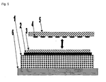
- the first layer (2) can also be a layer formed of metallic clusters, which is based on a carrier (1) is applied.
- the carrier (1) can be the carrier substrate to be marked.
- the inert spacer layer is designated by (3).
- the metallic clusters (4) are expediently made, for example, from copper.
- Fig. 3 to 5 is provided for further processing of the counterfeit-proof marked carrier substrate adhesive or lamination with (6). The change in the reflected light which produces the characteristic color spectrum in comparison with the incident light is visualized in an arrow in these two figures by means of the gray scale profile.
- a made of metallic clusters third layer (4) is applied.
- the second layer (3) is applied to a mirror layer (2).
- the mirror layer is applied to a carrier substrate (1).
- the third layer (4) formed of metallic clusters is applied first, then the second layer (3), then the mirror layer (2) and finally the adhesive or lamination layer (6).
- marks is only the optically transparent formed second layer (3) on the electromagnetically reflecting first layer (2) and this applied to a carrier substrate (1).
- the marking is initially not visible.
- the markings are only visible when they are brought into contact with a substrate (5) on the surface of which the third layer (4) formed of metallic clusters is applied. This in turn produces a color effect that can be observed through the substrate (5).
- the carrier substrate (5) is expediently made of a transparent material, for example of plastic such as polyethylene terephthalate polycarbonate, polyurethane, polyethylene, polypropylene, polyacrylate, polyvinyl chloride, polyepoxide.
- coated support materials produced according to the invention can be used as security features in data carriers, value documents, labels, labels, seals, in packaging, textiles and the like.
- the sol (almost pH neutral, hardly any salt) is rebuffered by adding 5 ml of 1 M sodium carbonate solution (pH 9.6). Only sufficiently protected clusters remain in solution and do not precipitate.
- the sol can be concentrated by centrifugation or binds directly after application to the nitrocellulose coated surface. With a suitable choice of Nitrocellulose layer thickness develop after drying of the excess water strong surface dyeings.
- the sol after concentration, is added by a factor of 10 small amounts (e.g., 5%) of a neutral polymer (e.g., PVA).
- PVA neutral polymer
- the colloids are dry randomly oriented with the polymer in a very thin layer. There are observed as in Example 1c) characteristic colors.
- a Cu layer with a thickness of 4 nm is sputtered onto a web-shaped carrier substrate, which is already provided with a mirror layer and a nitrocellulose layer as a transparent spacer layer.
- the sputtering is carried out by means of a magnetron plasma source with a power of 20 W / cm 2 at 25 ° C using Ar with a partial pressure of 5 x 10 -3 mbar as a process gas.
- the speed of the web is 0.5m / s.
- the Cu layer shows pronounced island growth.
- the islands with a mean diameter of a few nm correspond to the clusters in the wet-chemical process. Significantly different characteristic color spectra are observed.
Description
Die Erfindung betrifft ein Verfahren zur Herstellung fälschungssicherer Identifikationsmerkmale, die einen Farbkippeffekt, bewirkt durch metallische Cluster, die über eine definierte transparente Schicht von einer Spiegelschicht getrennt sind, aufweisen.The invention relates to a method for producing tamper-proof identification features, which have a color shift effect, caused by metallic clusters, which are separated by a defined transparent layer of a mirror layer.
Aus
Aufgabe der Erfindung ist es ein Verfahren zur Herstellung von fälschungssicheren Identifikationsmerkmalen auf flexiblen Materialien bereitzustellen, wobei die Fälschungssicherheit durch eine sichtbare Farbänderung unter verschiedenen Betrachtungswinkeln (Kippeffekt), die auch maschinenlesbar sein soll, gegeben ist. Im maschinell ausgelesenen Spektrum soll das Herstellungsverfahren eindeutig codiert werden.The object of the invention is to provide a method for producing forgery-proof identification features on flexible materials, wherein the security against counterfeiting is given by a visible color change at different viewing angles (tilting effect), which should also be machine-readable. In the machine-read spectrum, the manufacturing process should be clearly coded.
Gegenstand der Erfindung ist daher ein Verfahren zur Herstellung von fälschungssicheren Identifikationsmerkmalen bestehend aus jeweils mindestens einer elektromagnetische Wellen reflektierenden Schicht (2), einer optisch transparent ausgebildeten Abstandsschicht (3) und einer Schicht gebildet von metallischen Clustem (4).The invention therefore provides a method for producing tamper-resistant identification features consisting of at least each an electromagnetic wave reflecting layer (2), an optically transparent spacer layer (3) and a layer formed by metallic clusters (4).
Die weiteren wesentlichen Merkmale der Erfindung sind in den unabhängigen Ansprüchen 1 bis 3 definiert.The other essential features of the invention are defined in the
Als Trägersubstrat kommen vorzugsweise flexible Kunststofffolien, beispielsweise aus PI, PP, MOPP, PE, PPS, PEEK, PEK, PEI, PSU, PAEK, LCP, PEN, PBT, PET, PA, PC, COC, POM, ABS, PVC in Frage. Die Trägerfolien weisen vorzugsweise eine Dicke von 5 - 700 µm, bevorzugt 8 - 200 µm, besonders bevorzugt 12 - 50 µm auf.
Ferner können als Trägersubstrat auch Metallfolien, beispielsweise Al-, Cu-, Sn-, Ni-, Fe- oder Edelstahlfolien mit einer Dicke von 5 - 200 µm, vorzugsweise 10 bis 80 µm, besonders bevorzugt 20 - 50 µm dienen. Die Folien können auch oberflächenbehandelt, beschichtet oder kaschiert, beispielsweise mit Kunststoffen, oder lackiert sein.
Ferner können als Trägersubstrate auch zellstofffreies oder zellstoffhaltiges Papier, thermoaktivierbares Papier oder Verbunde mit Papier, beispielsweise Verbunde mit Kunststoffen mit einem Flächengewicht von 20 - 500 g/m2, vorzugsweise 40 - 200 g/m2, verwendet werden.Suitable carrier substrates are preferably flexible plastic films, for example of PI, PP, MOPP, PE, PPS, PEEK, PEK, PEI, PSU, PAEK, LCP, PEN, PBT, PET, PA, PC, COC, POM, ABS, PVC , The carrier films preferably have a thickness of 5 to 700 .mu.m, preferably 8 to 200 .mu.m, more preferably 12 to 50 .mu.m.
Furthermore, metal foils, for example Al, Cu, Sn, Ni, Fe or stainless steel foils having a thickness of 5-200 μm, preferably 10 to 80 μm, particularly preferably 20-50 μm, may also serve as the carrier substrate. The films can also be surface-treated, coated or laminated, for example with plastics, or painted.
Furthermore, as carrier substrates, pulp-free or cellulose-containing paper, heat-activatable paper or composites with paper, for example composites with plastics having a basis weight of 20-500 g / m 2 , preferably 40-200 g / m 2 , may be used.
Auf das Trägersubstrat wird eine elektromagnetische Wellen reflektierende Schicht aufgebracht. Diese Schicht kann vorzugsweise aus Metallen, wie beispielsweise Aluminium, Gold, Chrom, Silber, Kupfer, Zinn, Platin, Nickel und deren Legierungen, beispielsweise Nickel/Chrom, Kupfer/Aluminium und dergleichen bestehen.An electromagnetic wave reflecting layer is applied to the carrier substrate. This layer may preferably be made of metals such as aluminum, gold, chromium, silver, copper, tin, platinum, nickel and their alloys, for example nickel / chromium, copper / aluminum and the like exist.
Die elektromagnetische Wellen reflektierende Schicht kann vollflächig oder partiell durch bekannte Verfahren, wie Sprühen, Bedampfen, Sputtern, Drucken (Tief-, Flexo-, Sieb-, Digitaldruck), Lackieren, Walzenauftragsverfahren und dergleichen aufgebracht werden.The electromagnetic wave reflecting layer may be applied all over or partially by known methods such as spraying, vapor deposition, sputtering, printing (gravure, flexographic, screen, digital printing), painting, roller coating and the like.
Zur partiellen Aufbringung eignet sich besonders ein Verfahren unter Verwendung eines löslichen Farbauftrags zur Herstellung der partiellen Metallisierung. Dabei wird in einem ersten Schritt auf dem Trägersubstrat ein in einem Lösungsmittel löslicher Farbauftrag aufgebracht, in einem zweiten Schritt diese Schicht gegebenenfalls mittels eines Inline-Plasma-, Corona- oder Flammprozesses behandelt und in einem dritten Schritt eine Schicht des zu strukturierenden Metalls bzw. der Metalllegierung aufgebracht, worauf in einem vierten Schritt der Farbauftrag mittels eines Lösungsmittels, gegebenenfalls kombiniert mit einer mechanischen Einwirkung, entfernt wird.
Der lösliche Farbauftrag kann vollflächig oder partiell erfolgen, die Aufbringung des Metalls bzw. der Metalllegierung erfolgt vollflächig oder partiell.For partial application, a method using a soluble paint for producing the partial metallization is particularly suitable. In this case, in a first step, a solvent-soluble paint application is applied to the carrier substrate, in a second step this layer optionally treated by means of an in-line plasma, corona or flame process and in a third step, a layer of the metal to be structured or In a fourth step, the paint application by means of a solvent, optionally combined with a mechanical action, is removed.
The soluble application of paint can be carried out over the entire surface or partially, the application of the metal or the metal alloy takes place over the entire surface or partially.
Die Aufbringung des Farbauftrags kann durch ein beliebiges Verfahren, beispielsweise durch Tiefdruck, Flexodruck, Siebdruck, Digitaldruck und dergleichen erfolgen. Die verwendete Farbe bzw. der verwendete Lack ist in einem Lösungsmittel, vorzugsweise in Wasser löslich, es kann jedoch auch eine in jedem beliebigen Lösungsmittel, beispielsweise in Alkohol, Estern und dergleichen lösliche Farbe verwendet werden. Die Farbe bzw. der Lack können übliche Zusammensetzungen auf Basis von natürlichen oder künstlichen Makromolekülen sein. Die lösliche Farbe kann pigmentiert oder nicht pigmentiert sein. Als Pigmente können alle bekannten Pigmente verwendet werden. Besonders geeignet sind TiO2, ZnS, Kaolin und dergleichen.The application of the paint can be done by any method, for example by gravure printing, flexographic printing, screen printing, digital printing and the like. The paint or varnish used is soluble in a solvent, preferably water, but it is also possible to use a paint which is soluble in any solvent, for example in alcohol, esters and the like. The paint or lacquer may be conventional compositions based on natural or artificial macromolecules. The soluble color may be pigmented or unpigmented. As pigments, all known pigments can be used. Particularly suitable are TiO 2 , ZnS, kaolin and the like.
Anschließend wird das bedruckte Trägersubstrat gegebenenfalls mittels eines Inline-Plasma- (Niederdruck- oder Atmosphärenplasma-), Corona- oder Flammprozesses behandelt. Durch energiereiches Plasma, beispielsweise Ar- oder Ar/O2-Plasma wird die Oberfläche von Tonungsresten der Druckfarben gereinigt.Subsequently, the printed carrier substrate is optionally treated by means of an in-line plasma (low pressure or atmospheric plasma), corona or flame process. High-energy plasma, for example Ar or Ar / O 2 plasma, cleans the surface of toning residues of the printing inks.
Gleichzeitig wird die Oberfläche aktiviert. Dabei werden endständige polare Gruppen an der Oberfläche erzeugt. Dadurch wird die Haftung von Metallen und dergleichen an der Oberfläche verbessert.At the same time, the surface is activated. In this case, terminal polar groups are generated on the surface. This improves the adhesion of metals and the like to the surface.
Gegebenenfalls kann gleichzeitig mit der Anwendung der Plasma- bzw. Corona- oder Flammbehandlung oder im Anschluss daran, eine dünne Metall- oder Metalloxidschicht als Haftvermittler, beispielsweise durch Sputtern oder Aufdampfen aufgebracht werden. Besonders geeignet sind dabei Cr, Al, Ag, Ti, Cu, TiO2, Si-Oxide oder Chromoxide. Diese Haftvermittlerschicht weist im allgemeinen eine Dicke von 0,1 nm - 5nm, vorzugsweise 0,2 nm - 2nm, besonders bevorzugt 0,2 nm bis 1 nm auf.Optionally, simultaneously with the application of the plasma or corona or flame treatment or subsequently, a thin metal or metal oxide layer can be applied as adhesion promoter, for example by sputtering or vapor deposition. Particularly suitable are Cr, Al, Ag, Ti, Cu, TiO 2 , Si oxides or chromium oxides. This adhesion promoter layer generally has a thickness of 0.1 nm-5 nm, preferably 0.2 nm-2 nm, particularly preferably 0.2 nm to 1 nm.
Dadurch wird die Haftung der partiell oder vollflächig aufgebrachten elektromagnetische Wellen reflektierenden Metall- bzw. Metalllegierungsschicht weiter verbessert.As a result, the adhesion of the partially or completely applied electromagnetic waves reflecting metal or metal alloy layer is further improved.
Eine partielle, elektromagnetische Wellen reflektierende Schicht kann aber auch durch ein übliches bekanntes Ätzverfahren hergestellt werden.However, a partial electromagnetic wave reflecting layer can also be produced by a conventionally known etching method.
Die Dicke der elektromagnetische Wellen reflektierenden Schicht beträgt vorzugsweise etwa 10 - 50 nm, wobei aber auch höhere bzw. geringere Schichtdicken möglich sind.
Werden Metallfolien als Trägersubstrat verwendet, so kann das Trägersubstrat selbst bereits die elektromagnetische Wellen reflektierende Schicht bilden. Vorzugsweise beträgt die Reflexion dieser Schicht für elektromagnetische Wellen, insbesondere in Abhängigkeit von der Dicke der Schicht bzw. der verwendeten Metallfolie 10 -100%.The thickness of the electromagnetic wave reflecting layer is preferably about 10 - 50 nm, but also higher or lower layer thicknesses are possible.
If metal foils are used as the carrier substrate, the carrier substrate itself may already form the electromagnetic wave reflecting layer. The reflection of this layer for electromagnetic waves, in particular as a function of the thickness of the layer or the metal foil used, is preferably 10 -100%.
Die darauf folgende polymere Schicht bzw. die polymeren Schichten können ebenfalls vollflächig oder partiell aufgebracht werden.
Die polymeren Schichten bestehen beispielsweise aus Farb- oder Lacksystemen auf Basis von Nitrocellulose, Epoxy-, Polyester-, Kolophonium-, Acrylat-, Alkyd-, Melamin-, PVA-, PVC-, Isocyanat- oder Urethansystemen.The following polymeric layer or layers can also be applied over the entire surface or partially.
The polymeric layers consist for example of paint or paint systems based on nitrocellulose, epoxy, polyester, rosin, acrylate, alkyd, melamine, PVA, PVC, isocyanate or urethane systems.
Diese polymere Schicht dient im wesentlichen als transparente Abstandsschicht, kann aber je nach Zusammensetzung in einem bestimmten Spektralbereich absorbierend sein. Gegebenenfalls kann diese absorbierende Eigenschaft auch durch Beimengung eines geeigneten Chromophors verstärkt werden. Durch die Auswahl verschiedener Chromophore kann ein geeigneter Spektralbereich ausgewählt werden. Dadurch kann neben dem Kippeffekt auch die polymere Schicht zusätzlich maschinenlesbar gestaltet werden. So kann beispielsweise im blauen Spektralbereich (im Bereich von etwa 400 nm) ein gelber AZO-Farbstoff, beispielsweise Anilide; Rodural, Eosin, eingesetzt werden. Der Farbstoff verändert darüber hinaus das Spektrum der Markierung in charakteristischer Weise.This polymeric layer essentially serves as a transparent spacer layer but, depending on the composition, may be absorbent in a particular spectral range. Optionally, this absorbing property can also be enhanced by the addition of a suitable chromophore. By choosing different chromophores, a suitable spectral range can be selected. As a result, in addition to the tilting effect, the polymeric layer can additionally be made machine-readable. Thus, for example, in the blue spectral range (in the range of about 400 nm) a yellow AZO dye, for example anilides; Rodural, Eosin, are used. The dye also changes the spectrum of the label in a characteristic manner.
Diese polymere Schicht kann, in Abhängigkeit von der Qualität der Adhäsion auf der Trägerbahn bzw. einer gegebenenfalls darunter liegenden Schicht Entnetzungseffekte zeigen, was zu einer charakteristischen, makroskopischen lateralen Strukturierung führt.
Diese Strukturierung lässt sich beispielsweise durch Modifikation der Oberflächenenergie der Schichten, beispielsweise durch Plasmabehandlung, Coronabehandlung, Elektronen-, Ionenstrahlbehandlung oder durch Lasermodifikation gezielt verändern.
Ferner ist es möglich eine Haftvermittlerschicht mit bereichsweise unterschiedlicher Oberflächenenergie aufzubringen.Depending on the quality of the adhesion on the carrier web or on an optionally underlying layer, this polymeric layer may show wetting effects, which leads to a characteristic macroscopic lateral structuring.
This structuring can be modified, for example, by modification of the surface energy of the layers, for example by plasma treatment, corona treatment, electron beam, ion beam treatment or by laser modification.
Furthermore, it is possible to apply a primer layer with regions of different surface energy.
Die polymere Schicht weist eine definierte Dicke, vorzugsweise 10 nm bis 3 µm, besonders bevorzugt 100 - 1000 nm auf. Werden mehrere polymere Schichten aufgebracht, können diese jeweils unterschiedliche Dicken aufweisen.The polymeric layer has a defined thickness, preferably 10 nm to 3 μm, more preferably 100-1000 nm. If a plurality of polymeric layers are applied, they can each have different thicknesses.
Die polymere Schicht wird durch Aufstreichen, Lackieren, Gießen, Sprühen, Drucken (Siebdruck-, Tiefdruck- Flexodruck, oder Digitaldruckverfahren) oder Walzenauftragsverfahren aufgebracht.The polymeric layer is applied by brushing, painting, casting, spraying, printing (screen, gravure, or digital printing) or roller coating.
Die polymere Schicht wird in einem Verfahren aufgebracht, das die Aufbringung sehr homogener Schichtdicken über große Flächen erlaubt. Eine homogene Schichtdicke ist deshalb erforderlich um im fertigen Produkt eine gleichmäßige Farberscheinung zu gewährleisten. Die Toleranzen betragen nicht mehr als ± 5%, vorzugsweise ≤ ±2%.The polymeric layer is applied in a process that allows the application of very homogeneous layer thicknesses over large areas. A homogeneous layer thickness is therefore necessary to ensure a uniform color appearance in the finished product. The tolerances are not more than ± 5%, preferably ≤ ± 2%.
Besonders geeignet ist dabei ein Druckverfahren, wobei die Farbe oder der Lack aus einer temperaturgeregelten Lackwanne über einen Tauchzylinder und eine Übertragswalze auf den Druckzylinder aufgebracht wird, wobei im wesentlichen nur die Vertiefungen des Druckzylinders mit der Farbe oder dem Lack gefüllt werden. Mittels einer Rakel wird überschüssige Farbe oder Lack abgestreift und gegebenenfalls mittels einer Blasleiste weiter abgetrocknet.Particularly suitable is a printing process, wherein the color or paint is applied from a temperature-controlled paint pan via a plunger cylinder and a transfer roller on the printing cylinder, wherein only the wells of the printing cylinder are filled with the paint or the paint substantially. By means of a squeegee excess paint or varnish is stripped off and optionally further dried by means of a blow bar.
Auf die polymere Schicht wird anschließend eine Schicht gebildet aus metallischen Cluster aufgebracht. Die metallischen Cluster können beispielsweise aus Aluminium, Gold, Palladium, Platin, Chrom, Silber, Kupfer, Nickel und dergleichen oder deren Legierungen, wie beispielsweise Au/Pd oder Cr/Ni bestehen.
Diese Clusterschicht wird durch Sputtern (beispielsweise Ionenstrahl oder Magnetron) oder Verdampfen (Elektronenstrahl) aus einer Lösung oder durch Adsorption aufgebracht.On the polymeric layer is then applied a layer formed of metallic clusters. The metallic clusters may consist, for example, of aluminum, gold, palladium, platinum, chromium, silver, copper, nickel and the like or their alloys, such as, for example, Au / Pd or Cr / Ni.
This cluster layer is deposited by sputtering (for example ion beam or magnetron) or evaporation (electron beam) from a solution or by adsorption.
Bei der Herstellung der Clusterschicht in Vakuumprozessen kann vorteilhafterweise das Wachstum der Cluster und damit deren Form sowie die optischen Eigenschaften durch Einstellung der Oberflächenenergie oder der Rauhigkeit der darunterliegenden Schicht beeinflusst werden. Dies verändert in charakteristischer Weise die Spektren. Dies kann beispielsweise durch thermische Behandlung im Beschichtungsprozess oder durch Vorheizen des Substrats erfolgen.
So kann zum Beispiel die Form und damit auch die optischen Eigenschaften der Cluster durch Einstellung der Oberflächenenergie bzw. des Kondensationskoeffizienten des Metalls auf der darunterliegenden Schicht beeinflusst werden.
Diese Parameter können beispielsweise durch Behandlung der Oberfläche mit oxidierenden Flüssigkeiten, beispielsweise mit Na-Hypochlorit oder in einem PVD oder CVD-Prozess erfolgen.In the production of the cluster layer in vacuum processes, the growth of the clusters and thus their shape and the optical properties can advantageously be influenced by adjusting the surface energy or the roughness of the underlying layer. This characteristically changes the spectra. This can be done for example by thermal treatment in the coating process or by preheating the substrate.
Thus, for example, the shape and thus also the optical properties of the clusters can be influenced by adjusting the surface energy or the condensation coefficient of the metal on the underlying layer.
These parameters can be achieved, for example, by treatment of the surface with oxidizing liquids, for example with Na hypochlorite or in a PVD or CVD process.
Die Clusterschicht wird vorzugsweise mittels Sputtern aufgebracht. Dabei werden die Eigenschaften der Schicht, insbesondere die Dichte und die Struktur, vor allem durch die Leistungsdichte, die verwendete Gasmenge und deren Zusammensetzung, die Temperatur des Substrats und die Bahngeschwindigkeit eingestellt.The cluster layer is preferably applied by sputtering. The properties of the layer, in particular the density and the structure, are set above all by the power density, the amount of gas used and its composition, the temperature of the substrate and the web speed.
Beim Aufbringen aus der Lösung mittels nasschemischer Verfahren werden in einem ersten Schritt die Cluster in Lösung hergestellt, anschließend die Cluster derivatisiert, aufkonzentriert und direkt auf die polymere Oberfläche aufgebracht.When applied from the solution by wet-chemical methods, the clusters are prepared in solution in a first step, then the clusters are derivatized, concentrated and applied directly to the polymeric surface.
Zur Aufbringung mittels drucktechnischer Verfahren werden nach dem Aufkonzentrieren der Cluster geringe Mengen eines inerten Polymers, beispielsweise PVA, Polymethylmethacrylat, Nitrocellulose-, Polyester-oder Urethansysteme zugemischt. Die Mischung kann dann anschließend mittels eines Druckverfahrens, beispielsweise Sieb-, Flexo- oder vorzugsweise Tiefdruckverfahren auf die polymere Schicht aufgebracht werden.For application by means of printing technology, after concentrating the clusters, small amounts of an inert polymer, for example PVA, polymethyl methacrylate, nitrocellulose, polyester or urethane systems are admixed. The mixture can then be subsequently a printing process, such as screen, flexo or preferably gravure printing methods are applied to the polymeric layer.
Die Dicke der Clusterschicht beträgt vorzugsweise 2 - 20 nm, besonders bevorzugt 3-10 nm.The thickness of the cluster layer is preferably 2 to 20 nm, particularly preferably 3 to 10 nm.
Zusätzlich kann darüber eine Schutzschicht mit vakuumtechnischen oder drucktechnischen Verfahren aufgebracht werden.In addition, a protective layer can be applied by means of vacuum technology or printing technology.
In einer bevorzugten Ausführungsform wird die Polymerschicht durch Modifikation der Oberflächenenergie gezielt strukturiert.
Die Strukturen erscheinen dann durch die anschließend aufgebrachte Clusterschicht aufgrund des Farbeffekts sehr kontrastreich, wodurch sie für das Auge leicht erkennbar sind. Daher wird durch eine solche Strukturierung ein zusätzliches fälschungssicheres Merkmal erzeugt.In a preferred embodiment, the polymer layer is specifically structured by modifying the surface energy.
Due to the color effect, the structures then appear very rich in contrast due to the subsequently applied cluster layer, making them easily recognizable to the eye. Therefore, such structuring creates an additional tamper-proof feature.
Ferner kann diese Strukturierung durch Fingerprint-Algorithmen in eineindeutige Codes verwandelt werden, die dann maschinell auslesbar sind.
Dadurch kann eine Strukturierung einem definierten Zahlenwert zugeordnet werden, wobei Markierungen mit gleichen Herstellparametem, d.h. mit gleichem Farbeffekt, individualisierbar werden.Furthermore, this structuring can be transformed by fingerprint algorithms into one-to-one codes, which are then machine-readable.
As a result, a structuring can be assigned to a defined numerical value, whereby markings having the same manufacturing parameters, ie having the same color effect, can be individualized.
Zur Anwendung insbesondere als Sicherheitsmerkmal können die einzelnen Schichtkombinationen auch auf getrennten Substraten aufgebracht werden.
So kann beispielsweise die elektromagnetische Wellen reflektierende Schicht und die polymere Abstandsschicht auf einem ersten Substrat aufgebracht sein, das beispielsweise auf ein Wertdokument aufgebracht oder in dieses Wertdokument eingebracht sein kann. Auf ein weiteres Substrat kann dann die Clusterschicht aufgebracht sein, die gegebenenfalls mit einer Klebeschicht versehen ist. Durch Zusammenfügen der beiden beschichteten Substrate erscheint dann nach dem Schlüssel/Schloss-Prinzip der charakteristische Farbeffekt.For use in particular as a security feature, the individual layer combinations can also be applied to separate substrates.
Thus, for example, the electromagnetic wave reflecting layer and the polymeric spacer layer may be applied to a first substrate, which may for example be applied to a value document or incorporated into this value document. The cluster layer can then be applied to a further substrate, which is optionally provided with an adhesive layer. By joining the two coated substrates then appears according to the key / lock principle, the characteristic color effect.
Das Trägersubstrat kann auch bereits eine oder mehrere funktionelle und/oder dekorative Schichten aufweisen.
Als solche Farb- bzw. Lackschichten können jeweils verschiedenste Zusammensetzungen verwendet werden. Die Zusammensetzung der einzelnen Schichten kann insbesondere nach deren Aufgabe variieren, je nach dem ob die einzelnen Schichten ausschließlich Dekorationszwecken dienen oder eine funktionelle Schicht sein sollen oder ob die Schicht sowohl eine Dekorationsals auch eine funktionelle Schicht sein soll.The carrier substrate may also already have one or more functional and / or decorative layers.
As such color or lacquer layers, a wide variety of compositions can be used in each case. The composition of the individual layers may in particular vary according to their purpose, depending on whether the individual layers serve exclusively decorative purposes or should be a functional layer or whether the layer should be both a decorative and a functional layer.
Die zu druckenden Schichten können pigmentiert oder nicht pigmentiert sein. Als Pigmente können alle bekannten Pigmente, wie beispielsweise Titandioxid, Zinksulfid, Kaolin, ATO, FTO, ITO, Aluminium, Chrom- und Siliciumoxide als auch farbige Pigmente verwendet werden. Dabei sind lösungsmittelhaltige Lacksysteme als auch Systeme ohne Lösungsmittel verwendbar.
Als Bindemittel kommen verschiedene natürliche oder synthetische Bindemittel in Frage.The layers to be printed may be pigmented or unpigmented. As pigments, it is possible to use all known pigments, for example titanium dioxide, zinc sulfide, kaolin, ATO, FTO, ITO, aluminum, chromium oxides and silicon oxides, as well as colored pigments. In this case, solvent-based coating systems and systems without solvents can be used.
Suitable binders are various natural or synthetic binders.
Die funktionellen Schichten können beispielsweise bestimmte elektrische, magnetische, spezielle chemische, physikalische und auch optische Eigenschaften aufweisen.The functional layers may for example have certain electrical, magnetic, special chemical, physical and also optical properties.
Zur Einstellung elektrischer Eigenschaften, beispielsweise Leitfähigkeit können beispielsweise Graphit, Ruß, leitfähige organische oder anorganische Polymere. Metallpigmente (beispielsweise Kupfer, Aluminium, Silber, Gold, Eisen, Chrom Blei und dergleichen), Metallegierungen wie Kupfer-Zink oder Kupfer- Aluminium oder deren Sulfide oder Oxide, oder auch amorphe oder kristalline keramische Pigmente wie ITO und dergleichen zugegeben werden. Weiters können auch dotierte oder nicht dotierte Halbleiter wie beispielsweise Silicium, Germanium oder Ionenleiter wie amorphe oder kristalline Metalloxide oder Metallsulfide als Zusatz verwendet werden. Ferner können zur Einstellung der elektrischen Eigenschaften der Schicht polare oder teilweise polare Verbindungen, wie Tenside oder unpolare Verbindungen wie Silikonadditive oder hygroskopische oder nicht hygroskopische Salze verwendet oder zugesetzt werden.To adjust electrical properties, such as conductivity, for example, graphite, carbon black, conductive organic or inorganic polymers. Metal pigments (for example, copper, aluminum, silver, gold, iron, chromium lead and the like), metal alloys such as copper-zinc or copper-aluminum or their sulfides or oxides, or amorphous or crystalline ceramic pigments such as ITO and the like may be added. Furthermore, doped or non-doped semiconductors such as, for example, silicon, germanium or ion conductors such as amorphous or crystalline metal oxides or metal sulfides can also be used as an additive. Further, to adjust the electrical properties of the layer polar or partially polar Compounds such as surfactants or non-polar compounds such as silicone additives or hygroscopic or non-hygroscopic salts are used or added.
Zur Einstellung der magnetischen Eigenschaften können paramagnetische, diamagnetische und auch ferromagnetische Stoffe, wie Eisen, Nickel und Cobalt oder deren Verbindungen oder Salze (beispielsweise Oxide oder Sulfide) verwendet werden.To adjust the magnetic properties, paramagnetic, diamagnetic and also ferromagnetic substances, such as iron, nickel and cobalt or their compounds or salts (for example oxides or sulfides) can be used.
Die optischen Eigenschaften der Schicht lassen sich durch sichtbare Farbstoffe bzw. Pigmente, lumineszierende Farbstoffe bzw. Pigmente, die im sichtbaren, im UV-Bereich oder im IR-Bereich fluoreszieren bzw. phosphoreszieren, Effektpigmente, wie Flüssigkristalle, Perlglanz, Bronzen und/oder wärmeempfindliche Farben bzw. Pigmente beeinflussen. Diese sind in allen möglichen Kombinationen einsetzbar. Zusätzlich können auch phosphoreszierende Pigmente allein oder in Kombination mit anderen Farbstoffen und/oder Pigmenten eingesetzt werden.The optical properties of the layer can be visualized by visible dyes or pigments, luminescent dyes or pigments which fluoresce or phosphoresce in the visible, in the UV range or in the IR range, effect pigments, such as liquid crystals, pearlescent, bronzes and / or heat-sensitive Influence colors or pigments. These can be used in all possible combinations. In addition, phosphorescent pigments can also be used alone or in combination with other dyes and / or pigments.
Es können auch verschiedene Eigenschaften durch Zufügen verschiedener oben genannter Zusätze kombiniert werden. So ist es möglich angefärbte und/oder leitfähige Magnetpigmente zu verwenden. Dabei sind alle genannten leitfähigen Zusätze verwendbar.
Speziell zum Anfärben von Magnetpigmenten lassen sich alle bekannten löslichen und nicht löslichen Farbstoffe bzw. Pigmente verwenden. So kann beispielsweise eine braune Magnetfarbe durch Zugabe von Metallen in ihrem Farbton metallisch, z.B. silbrig eingestellt werden.Various properties can also be combined by adding various additives mentioned above. Thus, it is possible to use colored and / or conductive magnetic pigments. All mentioned conductive additives can be used.
Especially for the dyeing of magnetic pigments it is possible to use all known soluble and non-soluble dyes or pigments. Thus, for example, a brown magnetic ink can be adjusted to metallic, for example silvery, by adding metals in their color shade.
Ferner können beispielsweise Isolatorschichten aufgebracht werden. Als Isolatoren sind beispielsweise organische Substanzen und deren Derivate und Verbindungen, beispielsweise Farb- und Lacksysteme, z.B. Epoxy-, Polyester-, Kolophonium-, Acrylat-, Alkyd-, Melamin-, PVA-, PVC-, Isocyanat-, Urethansysteme, die strahlungshärtend sein können, beispielsweise durch Wärme- oder UV-Strahlung, geeignet.Furthermore, for example, insulator layers can be applied. As insulators, for example, organic substances and their derivatives and compounds, such as paint and coating systems, such as epoxy, polyester, rosin, acrylate, alkyd, melamine, PVA, PVC, isocyanate, Urethane systems that can be radiation-curing, for example, by heat or UV radiation suitable.
Diese Schichten können durch bekannte Verfahren, beispielsweise durch Bedampfen, Sputtern, Drucken (beispielsweise Tief-, Flexo-, Sieb-, Digitaldruck und dergleichen), Sprühen, Galvanisieren, Walzenauftragsverfahren und dergleichen aufgebracht werden. Die Dicke der funktionellen Schicht beträgt 0,001 bis 50 µm, vorzugsweise 0,1 bis 20 µm.These layers can be applied by known methods such as sputtering, sputtering, printing (e.g., gravure, flexo, screen, digital printing, and the like), spraying, electroplating, roller coating, and the like. The thickness of the functional layer is 0.001 to 50 μm, preferably 0.1 to 20 μm.
Durch ein- oder mehrmalige Wiederholung eines oder mehrerer beschriebener Verfahrensschritte können Multilayer-Aufbauten hergestellt werden, die in den übereinander aufgebrachten Schichten unterschiedliche Eigenschaften aufweisen. Es ist dabei möglich durch Kombination von verschiedenen Eigenschaften der einzelnen Schichten, beispielsweise Schichten mit unterschiedlicher Leitfähigkeit, Magnetisierbarkeit, optischen Eigenschaften, Absorptionsverhalten und dergleichen, Aufbauten zum Beispiel für Sicherheitselemente mit mehreren präzisen Echtheitsmerkmalen herzustellen.By repeating one or more described process steps one or more times, multilayer structures can be produced which have different properties in the layers applied one above the other. By combining different properties of the individual layers, for example layers having different conductivity, magnetizability, optical properties, absorption behavior and the like, it is possible to produce structures for security elements with several precise authenticity features, for example.
Die Schichten können jeweils vollflächig oder partiell bereits auf dem Substrat vorhanden sein, bzw. aufgebracht werden.The layers can be present on the substrate over the entire surface or partially already, or can be applied.
Dabei können die Verfahrensschritte beliebig oft wiederholt werden, wobei beispielsweise bei vollflächiger Aufbringung einer funktionellen Schicht der Farbauftrag gegebenenfalls entfallen kann.In this case, the process steps can be repeated as often as desired, wherein, for example, in full-surface application of a functional layer of the paint can be omitted if necessary.
Es können aber auch beispielsweise in bekannten Direktmetallisierungsverfahren oder in Metallisierungsverfahren mit Ätzen partielle Metallschichten bzw. in bekannten Mehrfarben-Druckverfahren weitere Schichten aufgebracht werden.However, it is also possible to apply, for example, in known direct metallization processes or in metallization processes with etching, partial metal layers or, in known multicolor printing processes, further layers.
Gegebenenfalls kann die so hergestellte beschichtete Folie auch noch durch eine Schutzlackschicht geschützt werden oder beispielsweise durch Kaschieren oder dergleichen weiterveredelt werden.Optionally, the coated film produced in this way can also be protected by a protective lacquer layer or further refined, for example, by laminating or the like.
Gegebenenfalls kann das Produkt mit einem siegelfähigen Kleber, beispielsweise einem Heiß- oder Kaltsiegelkleber auf das entsprechende Trägermaterial appliziert werden, oder beispielsweise bei der Papierherstellung für Sicherheitspapiere durch übliche Verfahren in das Papier eingebettet werden.Optionally, the product can be applied with a sealable adhesive, such as a hot or cold seal adhesive to the appropriate substrate, or embedded in paper for security papers by conventional methods, for example.
Diese Siegelkleber können mit sichtbaren oder im UV-Licht sichtbaren, fluoreszierenden, phosphoreszierenden oder Laser- und IR-Strahlung absorbierenden Merkmalen zur Erhöhung der Fälschungssicherheit ausgestattet sein. Diese Merkmale können auch in Form von Mustern oder Zeichen vorhanden sein oder farbliche Effekte zeigen, wobei im Prinzip beliebig viele Farben, vorzugsweise 1 bis 10 Farben oder Farbmischungen, möglich sind.These sealants can be equipped with visible or visible in UV light, fluorescent, phosphorescent or laser and IR radiation absorbing features to increase the security against counterfeiting. These features may also be present in the form of patterns or characters or show color effects, in principle any number of colors, preferably 1 to 10 colors or color mixtures, are possible.
Das Trägersubstrat kann bei einseitiger Beschichtung nach der Anwendung entfernt werden oder am Produkt verbleiben. Dabei kann die Trägerfolie gegebenenfalls auf der nicht beschichteten Seite besonders ausgerüstet werden, beispielsweise kratzfest, antistatisch und dergleichen. Gleiches gilt für eine etwaige Lackschicht auf dem Trägersubstrat.The carrier substrate may be removed after application or remain on the product in one-sided coating. In this case, the carrier film may optionally be specially equipped on the uncoated side, for example, scratch-resistant, antistatic and the like. The same applies to a possible lacquer layer on the carrier substrate.
Ferner kann der Schichtaufbau transferierbar oder nicht transferierbar eingestellt werden, gegebenenfalls mit einer Transferlackschicht, die gegebenenfalls eine Diffraktionsstruktur, beispielsweise eine Hologrammstruktur aufweisen kann, versehen sein.Furthermore, the layer structure can be set in a transferable or non-transferable manner, if appropriate with a transfer lacquer layer, which may optionally have a diffraction structure, for example a hologram structure.
Der erfindungsgemäße Aufbau kann auch invers auf dem Trägermaterial aufgebracht werden, wobei auf ein Trägersubstrat eine Schicht gebildet aus metallischen Clustern, die mittels eines vakuumtechnischen Verfahrens oder aus lösungsmittelbasierten Systemen hergestellt wird und anschließend eine oder mehrere partielle und/oder vollflächige polymere Schichten definierter Dicke aufgebracht werden und darauf eine partielle oder vollflächige elektromagnetische Wellen reflektierende Schicht auf die Abstandschicht, aufgebracht wird.The structure according to the invention can also be applied inversely to the carrier material, with a layer formed of metallic clusters, which are produced by means of a vacuum-technical method, on a carrier substrate is prepared from solvent-based systems and then one or more partial and / or full-surface polymeric layers of defined thickness are applied and then a partial or full-surface electromagnetic wave reflecting layer is applied to the spacer layer.
In den
Darin bedeuten 1 das Trägersubstrat, 2 die elektromagnetische Wellen reflektierende erste Schicht, 3 die transparente Schicht, 4 die aus metallischen Clustern aufgebaute Schicht, 5 ein optisch transparentes Substrat, 6 eine Klebe- bzw. Laminierschicht.
-
Fig. 1 zeigt eine schematische Querschnittsansicht einer ersten ständig sichtbaren Markierung auf einem Trägersubstrat, -
Fig. 2 eine schematische Querschnittsansicht einer nicht ständig sichtbaren ersten Markierung auf einem Trägersubstrat sowie einem zum Nachweis bzw. - zur Sichtbarmachung geeigneten zweiten Trägersubstrat,
-
Fig. 3 eine schematische Querschnittsansicht einer ständig sichtbaren ersten laminier- oder klebbaren Markierung, -
Fig. 4 eine schematische Querschnittsansicht einer weiteren ständig sichtbaren zweiten laminier- oder klebbaren Markierung. -
Fig. 5 eine schematische Querschnittsansicht einer nicht ständig sichtbaren ersten laminier oder klebbaren Markierung sowie einem zum Nachweis bzw. - zur Sichtbarmachung geeigneten zweiten Trägersubstrat.
-
Fig. 6 ein im large-scale kontinuierlich beschichtetes fälschungssicher markiertes Trägersubstrat, welches teilweise auf Rollen aufgewickelt ist
Therein 1 denotes the carrier substrate, 2 the first layer reflecting the electromagnetic waves, 3 the transparent layer, 4 the layer composed of metallic clusters, 5 an optically transparent substrate, 6 an adhesive or laminating layer.
-
Fig. 1 shows a schematic cross-sectional view of a first permanently visible mark on a carrier substrate, -
Fig. 2 a schematic cross-sectional view of a not always visible first mark on a carrier substrate and a proof or - for visualization suitable second carrier substrate,
-
Fig. 3 a schematic cross-sectional view of a permanently visible first laminating or adhesive marker, -
Fig. 4 a schematic cross-sectional view of another constantly visible second laminating or adhesive marker. -
Fig. 5 a schematic cross-sectional view of a not permanently visible first laminating or adhesive label and a proof or - for visualization suitable second carrier substrate.
-
Fig. 6 a counterfeit-proof marked carrier substrate in a large-scale, which is partly wound up on rolls
Bei den in den
In den
In the
Bei den in den
In der
Bei den in
Die Funktion der Markierung ist folgende:
- Bei einer Einstrahlung von Licht aus einer Lichtquelle, wie einer Glühbirne, einem Laser, einer Leuchtstoffröhre, einer Halogenlampe, im speziellen einer Xenonlampe, auf eine der in
Fig. 1 ,3 und 4 gezeigten Markierungen wird dieses Licht an der ersten Schicht (2) reflektiert. Durch eine Wechselwirkung des reflektierten Lichts mit der aus der metallischen Clustern gebildeten dritten Schicht (4) wird ein Teil des eingestrahlten Lichts absorbiert. Das reflektierte Licht weist ein von mehreren Parametern, wie z.B. den optischen Konstanten des Schichtaufbaus, abhängiges, charakteristisches Spektrum auf. Die Markierung erscheint farbig. Die Färbung dient als fälschungssicherer Nachweis für die Echtheit der Markierung. Der so erhaltene Farbeindruck ist winkelabhängig und kann sowohl mit dem bloßen Auge als auch mit einem im Reflexionsmodus arbeitenden Lesegerät, vorzugsweise ein Spektralphotometer, identifiziert werden. Ein solches Photometer kann beispielsweise die Färbung der Oberflächen aus zwei verschiedenen Winkeln erfassen. Dies geschieht entweder mittels eines Detektors dadurch, dass zwei Lichtquellen verwendet werden, welche entsprechend angeschaltet werden und der Detektor entsprechend verkippt wird, oder dadurch dass zwei Photometer die aus zwei verschiedenen Winkeln beleuchtete Probe aus den beiden entsprechenden Winkeln vermessen.
- Upon irradiation of light from a light source, such as a light bulb, a laser, a fluorescent tube, a halogen lamp, in particular a xenon lamp, on one of the in
Fig. 1 .3 and 4 shown, this light is reflected on the first layer (2). By an interaction of the reflected light with the third layer (4) formed from the metallic clusters, part of the incident light is absorbed. The reflected light has one of several parameters, such as the optical constants of the layer structure, dependent, characteristic spectrum. The marking appears colored. The staining serves as a forgery proof for the authenticity of the mark. The color impression thus obtained is dependent on the angle and can be identified both with the naked eye and with a reader operating in reflection mode, preferably a spectrophotometer. For example, such a photometer can detect the coloration of surfaces from two different angles. This is done either by means of a detector in that two light sources are used, which are turned on accordingly and the detector is tilted accordingly, or in that two photometers measure the illuminated from two different angles sample from the two corresponding angles.
Hinsichtlich der für die Erzeugung der Wechselwirkungen einzuhaltenden Parameter wird auf die
Die erfindungsgemäß hergestellten beschichteten Trägermaterialien können als Sicherheitsmerkmale in Datenträgern, Wertdokumenten, Labels, Etiketten, Siegeln, in Verpackungen, Textilien und dergleichen verwendet werden.The coated support materials produced according to the invention can be used as security features in data carriers, value documents, labels, labels, seals, in packaging, textiles and the like.
100 ml aqua dest werden in einem 250 ml Kolben zum Sieden erhitzt. Unter starkem Rühren werden zuerst 4 ml 1 % triNatriumCitrat in aqua dest und dann 1 ml 1 % TetraChloroGoldsäure in aqua dest zugegeben. Innerhalb von 5 min verändert sich die Farbe des Reaktionsansatzes von nahezu farblos über Dunkelviolett zu Kirsch-Rot. Danach wird die Wärmezufuhr unterbunden und der Ansatz ca. 10 min weiter gerührt. Die Analyse des resultierenden Sols mit dem Transmissionselektronenmikroskop zeigt sphärische Partikel eines mittleren Durchmessers von 14 nm. Die Größenverteilung der Cluster ist eng (cv < 20%). Das Wellenlängen-Maximum der optischen Absorption liegt bei 518 nm.100 ml of distilled water are boiled in a 250 ml flask. With vigorous stirring, first 4 ml of 1% trisodium citrate in distilled water and then 1 ml of 1% TetraChloroGoldsäure in distilled water. Within 5 minutes, the color of the reaction mixture changes from almost colorless to dark purple to cherry red. Thereafter, the heat is suppressed and the approach stirred for about 10 min on. The analysis of the resulting sol with the transmission electron microscope shows spherical particles of a mean diameter of 14 nm. The size distribution of the clusters is narrow (cv <20%). The wavelength maximum of the optical absorption is 518 nm.
Zu 100 ml Gold Sol entsprechend der obigen Synthese wird unter starkem Rühren 1 ml einer 1%igen Lösung von BSA (Bovines Serum Albumin) in aqua dest gegeben. Die Lösung verfärbt sich leicht von Kirsch-Rot in ein dunkleres Rot. Das Maximum der optischen Absorption bleibt erhalten. Die Absorption im Wellenlängenbereich von 550 nm und höher nimmt zu. Im Transmissionselektronenmikroskop sind definierte Abstände zwischen den Partikeln erkennbar.To 100 ml of gold sol according to the above synthesis, 1 ml of a 1% solution of BSA (bovine serum albumin) in distilled water is added with vigorous stirring. The solution turns slightly from cherry red to a darker red. The maximum of optical absorption is retained. The absorption in the wavelength range of 550 nm and higher increases. In the transmission electron microscope, defined distances between the particles can be recognized.
Das Sol (nahezu pH neutral, kaum Salz) wird durch Zugabe von 5 ml 1 M Natrium-Carbonat-Lösung (pH 9,6) umgepuffert. Nur ausreichend geschützte Cluster bleiben in Lösung und präzipitieren nicht. Das Sol kann durch Zentrifugation aufkonzentriert werden oder bindet direkt nach Aufbringung an die mit Nitrocellulose beschichtete Oberfläche. Bei geeigneter Wahl der Nitrocellulose- Schichtdicke bilden sich nach Abtrocknen des überschüssigen Wassers starke Oberflächenfärbungen aus.The sol (almost pH neutral, hardly any salt) is rebuffered by adding 5 ml of 1 M sodium carbonate solution (pH 9.6). Only sufficiently protected clusters remain in solution and do not precipitate. The sol can be concentrated by centrifugation or binds directly after application to the nitrocellulose coated surface. With a suitable choice of Nitrocellulose layer thickness develop after drying of the excess water strong surface dyeings.
Dem Sol werden nach Aufkonzentrierung um einen Faktor 10 geringe Mengen (z.B. 5%) eines neutralen Polymers (z.B. PVA) beigemengt. Dadurch wird ein Verdrucken mit herkömmlichen Tiefdruckzylindern möglich. Die Kolloide trocken zufällig orientiert mit dem Polymer in einer sehr dünnen Schicht ein. Es werden wie in Beispiel 1c) charakteristische Farben beobachtet.The sol, after concentration, is added by a factor of 10 small amounts (e.g., 5%) of a neutral polymer (e.g., PVA). This makes it possible to print with conventional gravure cylinders. The colloids are dry randomly oriented with the polymer in a very thin layer. There are observed as in Example 1c) characteristic colors.
Unter Hochvakuumbedingungen (Basisdruck p<1x10⁻³ mbar) wird auf ein bahnförmiges Trägersubstrat, das bereits mit einer Spiegelschicht und einer Nitrocelluloseschicht als transparente Abstandsschicht versehen ist, eine Cu-Schicht mit einer Dicke von 4 nm aufgesputtert.Under high vacuum conditions (base pressure p <1x10 -3 mbar), a Cu layer with a thickness of 4 nm is sputtered onto a web-shaped carrier substrate, which is already provided with a mirror layer and a nitrocellulose layer as a transparent spacer layer.
Das Sputtern erfolgt mittels einer Magnetron-Plasma-Quelle mit einer Leistung von 20W/cm2 bei 25°C unter Verwendung von Ar mit einem Partialdruck von 5 x 10⁻³ mbar als Prozessgas. Die Geschwindigkeit der Bahn beträgt 0,5m/s. Unter diesen Bedingungen zeigt die Cu- Schicht ein ausgeprägtes Inselwachstum. Die Inseln mit einem mittleren Durchmesser von wenigen nm entsprechen den Clustern im nasschemischen Verfahren.
Es werden deutlich andere charakteristische Farbspektren beobachtet.The sputtering is carried out by means of a magnetron plasma source with a power of 20 W / cm 2 at 25 ° C using Ar with a partial pressure of 5 x 10 -3 mbar as a process gas. The speed of the web is 0.5m / s. Under these conditions, the Cu layer shows pronounced island growth. The islands with a mean diameter of a few nm correspond to the clusters in the wet-chemical process.
Significantly different characteristic color spectra are observed.
Claims (11)
- Method for producing tamper-proof identification elements each comprising at least one layer (2) reflecting electromagnetic waves, an optically transparent spacer layer (3) and a layer formed from metallic clusters (4), a layer (2) reflecting electromagnetic waves being applied to part or all of the surface of a carrier substrate (1), the optically transparent inert spacer layer (3) is applied to part or all of the surface of this layer reflecting electromagnetic waves, and a layer formed from metallic clusters (4) is applied to this optically transparent spacer layer, characterized in that the layer of metallic clusters (4) is applied by means of vacuum technology by sputtering or vapour deposition or from solvent-based systems by means of a wet chemical or printing method, and the optically transparent spacer layer (3) is formed from at least one polymer layer of defined thickness, which is applied by painting on, varnishing, casting, spraying, printing, for example screen-printing, gravure-printing, flexographic-printing or digital printing methods, or a roll application method, a homogenous layer thickness with a tolerance of ±5% being achieved.
- Method for producing tamper-proof identification elements each comprising at least one layer (2) reflecting electromagnetic waves, an optically transparent inert spacer layer (3) and a layer formed from metallic clusters (4), a layer formed from metallic clusters (4) being applied to a carrier substrate (1), the optically transparent inert spacer layer (3) being applied to part or all of the surface of this layer formed of metallic clusters, and the layer (2) reflecting electromagnetic waves being applied to part or all of the surface of this optically transparent inert spacer layer (3), characterized in that the layer of metallic clusters (4) is applied by means of vacuum technology by sputtering or vapour deposition or from solvent-based systems by means of a wet chemical or printing method, and the optically transparent spacer layer (3) is formed from at least one polymer layer of defined thickness, which is applied by painting on, varnishing, casting, spraying, printing, for example screen-printing, gravure-printing, flexographic-printing or digital printing methods, or a roll application method, a homogenous layer thickness with a tolerance of ±5% being achieved.
- Method for producing tamper-proof identification elements each comprising at least one layer (2) reflecting electromagnetic waves, an optically transparent inert spacer layer (3) and a layer formed from metallic clusters (4), a layer (2) reflecting electromagnetic waves being applied to a first carrier substrate (1), an optically transparent inert spacer layer (3) being applied to this layer (2) reflecting electromagnetic waves, and a layer formed from metallic clusters being applied to a second transparent carrier substrate (5), characterized in that only by joining the two carrier substrates coated in this way in such a way that the layer formed from metallic clusters (4) is joined to the spacer layer (3) is the tamper-proof identification element produced and can be detected, and the layer of metallic clusters (4) is applied by means of vacuum technology by sputtering or vapour deposition or from solvent-based systems by means of a wet chemical or printing method, and the optically transparent spacer layer (3) is formed from at least one polymer layer of defined thickness, which is applied by painting on, varnishing, casting, spraying, printing, for example screen-printing, gravure-printing, flexographic-printing or digital printing methods, or a roll application method, a homogenous layer thickness with a tolerance of ±5% being achieved.
- Method according to one of Claims 1 to 3, characterized in that a protective layer is applied to the layer formed from metallic clusters (4).
- Method according to one of Claims 1 to 4, characterized in that the layer (2) reflecting electromagnetic waves or the layer formed from metallic clusters (4), to which the optically transparent inert spacer layer (3) consisting of at least one polymer layer of defined thickness is applied, is modified by means of treatment with oxidizing liquids or by means of a PVD or CVD process.
- Method according to one of Claims 1 to 5, characterized in that the optically transparent inert spacer layer (3) consisting of at least one polymer layer of defined thickness is structured by means of de-wetting effects.
- Method according to Claim 6, characterized in that the de-wetting structures of the structured optically transparent spacer layer (3) consisting of at least one polymer layer of defined thickness are transformed into one-to-one codes by means of fingerprint algorithms.
- Method according to either of Claims 6 and 7, characterized in that the optically transparent spacer layer (3) consisting of at least one polymer layer of defined thickness is modified by means of treatment with sodium hypochlorite, by means of a PVD or CVD process.
- Method according to one of Claims 1 to 8, characterized in that the optically transparent polymer spacer layer (3) consisting of at least one polymer layer of defined thickness contains a chromophore.
- Method according to one of Claims 1 to 9, characterized in that further functional and/or decorative layers are applied to the carrier substrate or substrates (1, 5).
- Method according to one of Claims 1 to 10, characterized in that the carrier substrate or substrates is/are provided with a heat-sealing lacquer (6).
Applications Claiming Priority (3)
| Application Number | Priority Date | Filing Date | Title |
|---|---|---|---|
| AT0119102A AT413360B (en) | 2002-08-06 | 2002-08-06 | METHOD FOR PRODUCING FAKE-SECURE IDENTIFICATION FEATURES |
| AT11912002 | 2002-08-06 | ||
| PCT/EP2003/008327 WO2004014663A1 (en) | 2002-08-06 | 2003-07-28 | Method for producing tamper-proof identification elements |
Publications (2)
| Publication Number | Publication Date |
|---|---|
| EP1558449A1 EP1558449A1 (en) | 2005-08-03 |
| EP1558449B1 true EP1558449B1 (en) | 2016-01-06 |
Family
ID=31499787
Family Applications (1)
| Application Number | Title | Priority Date | Filing Date |
|---|---|---|---|
| EP03784094.9A Expired - Lifetime EP1558449B1 (en) | 2002-08-06 | 2003-07-28 | Method for producing tamper-proof identification elements |
Country Status (9)
| Country | Link |
|---|---|
| US (1) | US8067056B2 (en) |
| EP (1) | EP1558449B1 (en) |
| AT (1) | AT413360B (en) |
| AU (1) | AU2003253348A1 (en) |
| CA (1) | CA2494961C (en) |
| ES (1) | ES2564043T3 (en) |
| HU (1) | HUE027104T2 (en) |
| RU (1) | RU2297918C2 (en) |
| WO (1) | WO2004014663A1 (en) |
Cited By (1)
| Publication number | Priority date | Publication date | Assignee | Title |
|---|---|---|---|---|
| EP3233516B1 (en) | 2014-12-15 | 2020-06-03 | Hueck Folien Gesellschaft m.b.H. | Security element with colour shift effect and fluorescent features |
Families Citing this family (25)
| Publication number | Priority date | Publication date | Assignee | Title |
|---|---|---|---|---|
| DE10337331A1 (en) | 2003-08-12 | 2005-03-17 | Giesecke & Devrient Gmbh | Security element with thin-film element |
| DE102004042187B4 (en) | 2004-08-31 | 2021-09-09 | Infineon Technologies Ag | Chip card module for a contactless chip card with security marking |
| AT503714A2 (en) * | 2005-12-13 | 2007-12-15 | Hueck Folien Ges Mbh | SAFETY ELEMENTS AND SAFETY FEATURES WITH METALLICALLY APPEARING COLOR EFFECTS |
| US8070186B2 (en) * | 2006-05-31 | 2011-12-06 | Cabot Corporation | Printable reflective features formed from multiple inks and processes for making them |
| DE102006027263A1 (en) * | 2006-06-09 | 2007-12-13 | Identif Gmbh | Substrate with a layer sequence for producing a color impression which changes as a function of the viewing angle |
| AT505452A1 (en) * | 2007-04-16 | 2009-01-15 | Hueck Folien Gmbh | FALSE-SAFE IDENTIFICATION FEATURE |
| DE102007030017A1 (en) * | 2007-06-29 | 2009-01-08 | Matthias Lydike | Marking textiles |
| DE102007061979A1 (en) | 2007-12-21 | 2009-06-25 | Giesecke & Devrient Gmbh | security element |
| WO2009121605A2 (en) | 2008-04-02 | 2009-10-08 | Sicpa Holding S.A. | Identification and authentication using liquid crystal material markings |
| EP2127899A1 (en) | 2008-05-15 | 2009-12-02 | Hueck Folien Ges.m.b.H. | Tactile safety element |
| EP2159071B2 (en) | 2008-08-25 | 2022-01-12 | Hueck Folien Ges.m.b.H. | Safety element which can be verified without an aid |
| CN101730417B (en) * | 2008-10-31 | 2013-06-05 | 深圳富泰宏精密工业有限公司 | Housing and method for making same |
| CN101735678B (en) * | 2008-11-21 | 2013-01-09 | 鸿富锦精密工业(深圳)有限公司 | Colored coating and electronic product using same |
| AT507647B1 (en) * | 2008-12-11 | 2011-06-15 | Hueck Folien Gmbh | TRANSPARENT SAFETY ELEMENT |
| PE20100769A1 (en) | 2009-04-02 | 2010-11-25 | Sicpa Holding Sa | IDENTIFICATION AND AUTHENTICATION USING MARKINGS OF POLYMERIC LIQUID CRYSTAL MATERIAL |
| AT509928A2 (en) | 2010-05-26 | 2011-12-15 | Hueck Folien Gmbh | SECURITY ELEMENT WITH LIGHTING STRUCTURES |
| AT510220B1 (en) * | 2010-07-19 | 2013-07-15 | Hueck Folien Gmbh | SECURITY ELEMENT WITH AN OPTICAL VARIABLE LAYER |
| EP2578414B1 (en) | 2011-10-04 | 2013-12-11 | Hueck Folien Ges.m.b.H. | Security element with colour-switching effect, use of same and method for producing same |
| DE102011088154A1 (en) | 2011-12-09 | 2013-06-13 | CFC Europe GmbH | Layered product for coating and substrate used for hologram, has optical structure comprising layer(s) with high refractive nanoparticles and/or layer(s) with low refractive nanoparticles |
| DE102012018434A1 (en) | 2012-09-18 | 2014-03-20 | Giesecke & Devrient Gmbh | Optically variable security element with additional open / see-through effect |
| TW201522101A (en) * | 2013-07-10 | 2015-06-16 | Sicpa Holding Sa | Unique identifier and high security device related to said unique identifier |
| AT515670B1 (en) * | 2014-06-23 | 2015-11-15 | Hueck Folien Gmbh | Security element with modified color-shift effect |
| JP6874275B2 (en) * | 2016-04-04 | 2021-05-19 | 凸版印刷株式会社 | Information display medium and articles with information display medium |
| RU2628378C1 (en) * | 2016-09-29 | 2017-08-16 | Акционерное общество "ГОЗНАК" | Valuable document protected from forgery, and method of determining its authenticity |
| AT523690B1 (en) | 2020-03-16 | 2022-03-15 | Hueck Folien Gmbh | Flat security element with optical security features |
Citations (18)
| Publication number | Priority date | Publication date | Assignee | Title |
|---|---|---|---|---|
| US4639069A (en) | 1982-06-30 | 1987-01-27 | Teijin Limited | Optical laminar structure |
| US4705300A (en) | 1984-07-13 | 1987-11-10 | Optical Coating Laboratory, Inc. | Thin film optically variable article and method having gold to green color shift for currency authentication |
| US4856857A (en) | 1985-05-07 | 1989-08-15 | Dai Nippon Insatsu Kabushiki Kaisha | Transparent reflection-type |
| DE4017220A1 (en) | 1990-05-29 | 1991-01-31 | Tvg Thermo Vac Entwicklungs Gm | Multicolour coating layer on plastic films for interference filters - is produced on roll and has thin metal film, transparent varnish with varying thickness and final metal layer |
| US5278590A (en) | 1989-04-26 | 1994-01-11 | Flex Products, Inc. | Transparent optically variable device |
| US5611998A (en) | 1994-04-12 | 1997-03-18 | Avl Medical Instruments Ag | Optochemical sensor and method for production |
| WO1998048275A1 (en) | 1997-04-22 | 1998-10-29 | Thomas Schalkhammer | Reinforced cluster optical sensors |
| WO2000034395A1 (en) | 1998-12-07 | 2000-06-15 | Flex Products, Inc. | Bright metal flake based pigments |
| WO2001003945A1 (en) | 1999-07-08 | 2001-01-18 | Flex Products, Inc. | Diffractive surfaces with color shifting backgrounds |
| AT407165B (en) | 1999-03-23 | 2001-01-25 | Thomas Dr Schalkhammer | Thin-film structure for colouring metallic surfaces |
| WO2001053113A1 (en) | 2000-01-21 | 2001-07-26 | Flex Products, Inc. | Optically variable security devices |
| WO2002000445A1 (en) | 2000-06-28 | 2002-01-03 | De La Rue International Limited | Optically variable security device |
| WO2002018155A2 (en) | 2000-08-29 | 2002-03-07 | november Aktiengesellschaft Gesellschaft für Molekulare Medizin | Method for forgery-proof labeling of items, and forgery-proof label |
| WO2002031214A1 (en) | 2000-10-09 | 2002-04-18 | Hueck Folien | Metallized film, method for the production thereof, and its use |
| WO2002051646A1 (en) | 2000-12-22 | 2002-07-04 | Ovd Kinegram Ag | Decorative foil |
| WO2003016073A1 (en) | 2001-08-16 | 2003-02-27 | november Aktiengesellschaft Gesellschaft für Molekulare Medizin | Forgery-proof marking for objects and method for identifying such a marking |
| DE10208036A1 (en) | 2001-08-16 | 2003-08-21 | November Ag Molekulare Medizin | Forgery-proof marking system for e.g. check cards comprises plastic film and layers whose color varies with angle of observation, made up of absorbing layer of metal clusters, spacer and reflecting layers |
| WO2003095227A1 (en) | 2002-05-14 | 2003-11-20 | Leonhard Kurz Gmbh & Co. Kg | Optically variable element comprising a partially transparent element |
Family Cites Families (5)
| Publication number | Priority date | Publication date | Assignee | Title |
|---|---|---|---|---|
| US5286286A (en) * | 1991-05-16 | 1994-02-15 | Xerox Corporation | Colorless fast-drying ink compositions for printing concealed images detectable by fluorescence |
| JPH10100573A (en) | 1996-09-30 | 1998-04-21 | Toppan Printing Co Ltd | Paper and printed matter for preventing forgery |
| DE10035451C2 (en) * | 2000-07-19 | 2002-12-05 | November Ag Molekulare Medizin | Method and device for identifying a polymer sequence |
| US6498110B2 (en) * | 2001-03-05 | 2002-12-24 | Micron Technology, Inc. | Ruthenium silicide wet etch |
| US7322530B2 (en) * | 2001-08-16 | 2008-01-29 | November Aktiengesellschaft Gesellschaft Fur Molekulare Medizin | Forgery-proof marking for objects and method for identifying such a marking |
-
2002
- 2002-08-06 AT AT0119102A patent/AT413360B/en not_active IP Right Cessation
-
2003
- 2003-07-28 WO PCT/EP2003/008327 patent/WO2004014663A1/en not_active Application Discontinuation
- 2003-07-28 RU RU2005106243/11A patent/RU2297918C2/en active
- 2003-07-28 HU HUE03784094A patent/HUE027104T2/en unknown
- 2003-07-28 CA CA2494961A patent/CA2494961C/en not_active Expired - Fee Related
- 2003-07-28 EP EP03784094.9A patent/EP1558449B1/en not_active Expired - Lifetime
- 2003-07-28 US US10/523,825 patent/US8067056B2/en not_active Expired - Fee Related
- 2003-07-28 ES ES03784094.9T patent/ES2564043T3/en not_active Expired - Lifetime
- 2003-07-28 AU AU2003253348A patent/AU2003253348A1/en not_active Abandoned
Patent Citations (18)
| Publication number | Priority date | Publication date | Assignee | Title |
|---|---|---|---|---|
| US4639069A (en) | 1982-06-30 | 1987-01-27 | Teijin Limited | Optical laminar structure |
| US4705300A (en) | 1984-07-13 | 1987-11-10 | Optical Coating Laboratory, Inc. | Thin film optically variable article and method having gold to green color shift for currency authentication |
| US4856857A (en) | 1985-05-07 | 1989-08-15 | Dai Nippon Insatsu Kabushiki Kaisha | Transparent reflection-type |
| US5278590A (en) | 1989-04-26 | 1994-01-11 | Flex Products, Inc. | Transparent optically variable device |
| DE4017220A1 (en) | 1990-05-29 | 1991-01-31 | Tvg Thermo Vac Entwicklungs Gm | Multicolour coating layer on plastic films for interference filters - is produced on roll and has thin metal film, transparent varnish with varying thickness and final metal layer |
| US5611998A (en) | 1994-04-12 | 1997-03-18 | Avl Medical Instruments Ag | Optochemical sensor and method for production |
| WO1998048275A1 (en) | 1997-04-22 | 1998-10-29 | Thomas Schalkhammer | Reinforced cluster optical sensors |
| WO2000034395A1 (en) | 1998-12-07 | 2000-06-15 | Flex Products, Inc. | Bright metal flake based pigments |
| AT407165B (en) | 1999-03-23 | 2001-01-25 | Thomas Dr Schalkhammer | Thin-film structure for colouring metallic surfaces |
| WO2001003945A1 (en) | 1999-07-08 | 2001-01-18 | Flex Products, Inc. | Diffractive surfaces with color shifting backgrounds |
| WO2001053113A1 (en) | 2000-01-21 | 2001-07-26 | Flex Products, Inc. | Optically variable security devices |
| WO2002000445A1 (en) | 2000-06-28 | 2002-01-03 | De La Rue International Limited | Optically variable security device |
| WO2002018155A2 (en) | 2000-08-29 | 2002-03-07 | november Aktiengesellschaft Gesellschaft für Molekulare Medizin | Method for forgery-proof labeling of items, and forgery-proof label |
| WO2002031214A1 (en) | 2000-10-09 | 2002-04-18 | Hueck Folien | Metallized film, method for the production thereof, and its use |
| WO2002051646A1 (en) | 2000-12-22 | 2002-07-04 | Ovd Kinegram Ag | Decorative foil |
| WO2003016073A1 (en) | 2001-08-16 | 2003-02-27 | november Aktiengesellschaft Gesellschaft für Molekulare Medizin | Forgery-proof marking for objects and method for identifying such a marking |
| DE10208036A1 (en) | 2001-08-16 | 2003-08-21 | November Ag Molekulare Medizin | Forgery-proof marking system for e.g. check cards comprises plastic film and layers whose color varies with angle of observation, made up of absorbing layer of metal clusters, spacer and reflecting layers |
| WO2003095227A1 (en) | 2002-05-14 | 2003-11-20 | Leonhard Kurz Gmbh & Co. Kg | Optically variable element comprising a partially transparent element |
Non-Patent Citations (4)
| Title |
|---|
| "?Untersuchungen über den Aufbau aufgedampfter Metallschichten mittels Übermikroskop und Elektroneninterferenzen", HASS, COLLOID & POLYMER SCIENCE, vol. 100, no. 2, 1942, pages 230 - 242 |
| LEITNER, AUSSENEGG ET AL.: "Optical properties of a metal island film close to a smooth metal surface", APPLIED OPTICS, vol. 32, no. 1, 1993, pages 102 - 110, XP002574134 |
| RÖMPP LEXIKON, CHEMIE, 1999, pages 4204 |
| VAN RENESSE, ?OPTICAL DOCUMENT SECURITY, 1998, pages 289 - 322 |
Cited By (1)
| Publication number | Priority date | Publication date | Assignee | Title |
|---|---|---|---|---|
| EP3233516B1 (en) | 2014-12-15 | 2020-06-03 | Hueck Folien Gesellschaft m.b.H. | Security element with colour shift effect and fluorescent features |
Also Published As
| Publication number | Publication date |
|---|---|
| EP1558449A1 (en) | 2005-08-03 |
| ES2564043T3 (en) | 2016-03-17 |
| ATA11912002A (en) | 2005-07-15 |
| AU2003253348A8 (en) | 2004-02-25 |
| WO2004014663A1 (en) | 2004-02-19 |
| CA2494961C (en) | 2012-06-26 |
| US20060147640A1 (en) | 2006-07-06 |
| US8067056B2 (en) | 2011-11-29 |
| CA2494961A1 (en) | 2004-02-19 |
| RU2297918C2 (en) | 2007-04-27 |
| HUE027104T2 (en) | 2016-08-29 |
| AT413360B (en) | 2006-02-15 |
| AU2003253348A1 (en) | 2004-02-25 |
| RU2005106243A (en) | 2005-08-27 |
Similar Documents
| Publication | Publication Date | Title |
|---|---|---|
| EP1558449B1 (en) | Method for producing tamper-proof identification elements | |
| EP1716007B1 (en) | Tamper-proof, color-shift security feature | |
| EP2851194B1 (en) | Safety element, in particular safety label | |
| EP1291463A1 (en) | Process for producing a selectively metallized foil, and their products | |
| EP3233516A1 (en) | Security element with colour shift effect and fluorescent features and method for production and use of same | |
| EP1356952B1 (en) | Coated supporting substrate with different optical and/or fluorescent characteristics at both sides | |
| CN1860034B (en) | Security elements | |
| AT502319B1 (en) | SUBSTRATES WITH PREFERABLY TRANSFERABLE LAYERS AND / OR SURFACE STRUCTURES, METHOD FOR THEIR PRODUCTION AND THEIR USE | |
| EP1584647B1 (en) | Sheet material with optical features | |
| EP1871616A2 (en) | Security element having a spatially resolved magnetic coding, method and device for producing the same and the use thereof | |
| EP1318016A1 (en) | Method for superposing several layers printed in register, products printed with this method and their application | |
| AT500871A1 (en) | SAFETY ELEMENTS WITH VISUALLY RECOGNIZABLE AND MACHINE READABLE FEATURES | |
| EP1488935B1 (en) | Manufacturing process for a security element | |
| AT504631B1 (en) | FOIL MATERIALS, ESPECIALLY FOR SAFETY ELEMENTS | |
| EP1500521A2 (en) | Security elements with machine readable features and colour effects | |
| EP3486092B1 (en) | Method for production of a security element | |
| AT503712A2 (en) | CODED OPTICALLY ACTIVE SECURITY ELEMENTS AND SAFETY FEATURES | |
| EP1559540A1 (en) | Transfer film | |
| EP1647921A1 (en) | Data carrier comprising an individualised optically variable element |
Legal Events
| Date | Code | Title | Description |
|---|---|---|---|
| PUAI | Public reference made under article 153(3) epc to a published international application that has entered the european phase |
Free format text: ORIGINAL CODE: 0009012 |
|
| 17P | Request for examination filed |
Effective date: 20050519 |
|
| AK | Designated contracting states |
Kind code of ref document: A1 Designated state(s): AT BE BG CH CY CZ DE DK EE ES FI FR GB GR HU IE IT LI LU MC NL PT RO SE SI SK TR |
|
| AX | Request for extension of the european patent |
Extension state: AL LT LV MK |
|
| DAX | Request for extension of the european patent (deleted) | ||
| RIN1 | Information on inventor provided before grant (corrected) |
Inventor name: BERGSMANN, MARTIN Inventor name: WALTER, HARALD Inventor name: DOMNICK, RALPH Inventor name: BAUER, GEORG Inventor name: KASTNER, FRIEDRICH |
|
| RIN1 | Information on inventor provided before grant (corrected) |
Inventor name: WALTER, HARALD Inventor name: BERGSMANN, MARTIN Inventor name: KASTNER, FRIEDRICH Inventor name: BAUER, GEORG Inventor name: DOMNICK, RALPH |
|
| RIN1 | Information on inventor provided before grant (corrected) |
Inventor name: DOMNICK, RALPH Inventor name: WALTER, HARALD Inventor name: KASTNER, FRIEDRICH Inventor name: BAUER, GEORG Inventor name: BERGSMANN, MARTIN |
|
| RIN1 | Information on inventor provided before grant (corrected) |
Inventor name: WALTER, HARALD Inventor name: DOMNICK, RALPH Inventor name: BERGSMANN, MARTIN Inventor name: BAUER, GEORG Inventor name: KASTNER, FRIEDRICH |
|
| 17Q | First examination report despatched |
Effective date: 20071018 |
|
| RIN1 | Information on inventor provided before grant (corrected) |
Inventor name: BAUER, GEORG Inventor name: DOMNICK, RALPH Inventor name: BERGSMANN, MARTIN Inventor name: KASTNER, FRIEDRICH Inventor name: WALTER, HARALD |
|
| APBK | Appeal reference recorded |
Free format text: ORIGINAL CODE: EPIDOSNREFNE |
|
| APBN | Date of receipt of notice of appeal recorded |
Free format text: ORIGINAL CODE: EPIDOSNNOA2E |
|
| APBR | Date of receipt of statement of grounds of appeal recorded |
Free format text: ORIGINAL CODE: EPIDOSNNOA3E |
|
| APAF | Appeal reference modified |
Free format text: ORIGINAL CODE: EPIDOSCREFNE |
|
| APBT | Appeal procedure closed |
Free format text: ORIGINAL CODE: EPIDOSNNOA9E |
|
| GRAP | Despatch of communication of intention to grant a patent |
Free format text: ORIGINAL CODE: EPIDOSNIGR1 |
|
| RIC1 | Information provided on ipc code assigned before grant |
Ipc: B42D 25/00 20140101ALI20140325BHEP Ipc: B42D 15/00 20060101AFI20140325BHEP |
|
| INTG | Intention to grant announced |
Effective date: 20140414 |
|
| GRAS | Grant fee paid |
Free format text: ORIGINAL CODE: EPIDOSNIGR3 |
|
| 19U | Interruption of proceedings before grant |
Effective date: 20120321 |
|
| 19W | Proceedings resumed before grant after interruption of proceedings |
Effective date: 20151102 |
|
| GRAA | (expected) grant |
Free format text: ORIGINAL CODE: 0009210 |
|
| RAP1 | Party data changed (applicant data changed or rights of an application transferred) |
Owner name: HUECK FOLIEN GES.M.B.H |
|
| AK | Designated contracting states |
Kind code of ref document: B1 Designated state(s): AT BE BG CH CY CZ DE DK EE ES FI FR GB GR HU IE IT LI LU MC NL PT RO SE SI SK TR |
|
| REG | Reference to a national code |
Ref country code: GB Ref legal event code: FG4D Free format text: NOT ENGLISH |
|
| REG | Reference to a national code |
Ref country code: CH Ref legal event code: NV Representative=s name: BOVARD AG, CH Ref country code: CH Ref legal event code: EP |
|
| REG | Reference to a national code |
Ref country code: IE Ref legal event code: FG4D Free format text: LANGUAGE OF EP DOCUMENT: GERMAN |
|
| REG | Reference to a national code |
Ref country code: AT Ref legal event code: REF Ref document number: 768528 Country of ref document: AT Kind code of ref document: T Effective date: 20160215 |
|
| REG | Reference to a national code |
Ref country code: DE Ref legal event code: R096 Ref document number: 50315396 Country of ref document: DE |
|
| REG | Reference to a national code |
Ref country code: ES Ref legal event code: FG2A Ref document number: 2564043 Country of ref document: ES Kind code of ref document: T3 Effective date: 20160317 |
|
| REG | Reference to a national code |
Ref country code: SE Ref legal event code: TRGR |
|
| REG | Reference to a national code |
Ref country code: NL Ref legal event code: FP |
|
| REG | Reference to a national code |
Ref country code: FR Ref legal event code: PLFP Year of fee payment: 14 |
|
| PG25 | Lapsed in a contracting state [announced via postgrant information from national office to epo] |
Ref country code: GR Free format text: LAPSE BECAUSE OF FAILURE TO SUBMIT A TRANSLATION OF THE DESCRIPTION OR TO PAY THE FEE WITHIN THE PRESCRIBED TIME-LIMIT Effective date: 20160407 Ref country code: FI Free format text: LAPSE BECAUSE OF FAILURE TO SUBMIT A TRANSLATION OF THE DESCRIPTION OR TO PAY THE FEE WITHIN THE PRESCRIBED TIME-LIMIT Effective date: 20160106 |
|
| REG | Reference to a national code |
Ref country code: HU Ref legal event code: AG4A Ref document number: E027104 Country of ref document: HU |
|
| PG25 | Lapsed in a contracting state [announced via postgrant information from national office to epo] |
Ref country code: PT Free format text: LAPSE BECAUSE OF FAILURE TO SUBMIT A TRANSLATION OF THE DESCRIPTION OR TO PAY THE FEE WITHIN THE PRESCRIBED TIME-LIMIT Effective date: 20160506 |
|
| PGFP | Annual fee paid to national office [announced via postgrant information from national office to epo] |
Ref country code: NL Payment date: 20160720 Year of fee payment: 14 |
|
| REG | Reference to a national code |
Ref country code: DE Ref legal event code: R026 Ref document number: 50315396 Country of ref document: DE |
|
| PLBI | Opposition filed |
Free format text: ORIGINAL CODE: 0009260 |
|
| PG25 | Lapsed in a contracting state [announced via postgrant information from national office to epo] |
Ref country code: EE Free format text: LAPSE BECAUSE OF FAILURE TO SUBMIT A TRANSLATION OF THE DESCRIPTION OR TO PAY THE FEE WITHIN THE PRESCRIBED TIME-LIMIT Effective date: 20160106 Ref country code: DK Free format text: LAPSE BECAUSE OF FAILURE TO SUBMIT A TRANSLATION OF THE DESCRIPTION OR TO PAY THE FEE WITHIN THE PRESCRIBED TIME-LIMIT Effective date: 20160106 |
|
| PGFP | Annual fee paid to national office [announced via postgrant information from national office to epo] |
Ref country code: CH Payment date: 20160721 Year of fee payment: 14 |
|
| PLAX | Notice of opposition and request to file observation + time limit sent |
Free format text: ORIGINAL CODE: EPIDOSNOBS2 |
|
| 26 | Opposition filed |
Opponent name: GIESECKE & DEVRIENT GMBH Effective date: 20161005 |
|
| PG25 | Lapsed in a contracting state [announced via postgrant information from national office to epo] |
Ref country code: CZ Free format text: LAPSE BECAUSE OF FAILURE TO SUBMIT A TRANSLATION OF THE DESCRIPTION OR TO PAY THE FEE WITHIN THE PRESCRIBED TIME-LIMIT Effective date: 20160106 Ref country code: RO Free format text: LAPSE BECAUSE OF FAILURE TO SUBMIT A TRANSLATION OF THE DESCRIPTION OR TO PAY THE FEE WITHIN THE PRESCRIBED TIME-LIMIT Effective date: 20160106 Ref country code: SK Free format text: LAPSE BECAUSE OF FAILURE TO SUBMIT A TRANSLATION OF THE DESCRIPTION OR TO PAY THE FEE WITHIN THE PRESCRIBED TIME-LIMIT Effective date: 20160106 |
|
| PGFP | Annual fee paid to national office [announced via postgrant information from national office to epo] |
Ref country code: HU Payment date: 20160720 Year of fee payment: 14 Ref country code: SE Payment date: 20160720 Year of fee payment: 14 |
|
| PG25 | Lapsed in a contracting state [announced via postgrant information from national office to epo] |
Ref country code: BE Free format text: LAPSE BECAUSE OF NON-PAYMENT OF DUE FEES Effective date: 20160731 |
|
| PGFP | Annual fee paid to national office [announced via postgrant information from national office to epo] |
Ref country code: ES Payment date: 20160715 Year of fee payment: 14 |
|
| PG25 | Lapsed in a contracting state [announced via postgrant information from national office to epo] |
Ref country code: BG Free format text: LAPSE BECAUSE OF FAILURE TO SUBMIT A TRANSLATION OF THE DESCRIPTION OR TO PAY THE FEE WITHIN THE PRESCRIBED TIME-LIMIT Effective date: 20160406 Ref country code: SI Free format text: LAPSE BECAUSE OF FAILURE TO SUBMIT A TRANSLATION OF THE DESCRIPTION OR TO PAY THE FEE WITHIN THE PRESCRIBED TIME-LIMIT Effective date: 20160106 |
|
| PLBB | Reply of patent proprietor to notice(s) of opposition received |
Free format text: ORIGINAL CODE: EPIDOSNOBS3 |
|
| PG25 | Lapsed in a contracting state [announced via postgrant information from national office to epo] |
Ref country code: MC Free format text: LAPSE BECAUSE OF FAILURE TO SUBMIT A TRANSLATION OF THE DESCRIPTION OR TO PAY THE FEE WITHIN THE PRESCRIBED TIME-LIMIT Effective date: 20160106 |
|
| REG | Reference to a national code |
Ref country code: IE Ref legal event code: MM4A |
|
| PLBP | Opposition withdrawn |
Free format text: ORIGINAL CODE: 0009264 |
|
| REG | Reference to a national code |
Ref country code: FR Ref legal event code: PLFP Year of fee payment: 15 |
|
| PG25 | Lapsed in a contracting state [announced via postgrant information from national office to epo] |
Ref country code: IE Free format text: LAPSE BECAUSE OF NON-PAYMENT OF DUE FEES Effective date: 20160728 |
|
| PLBD | Termination of opposition procedure: decision despatched |
Free format text: ORIGINAL CODE: EPIDOSNOPC1 |
|
| REG | Reference to a national code |
Ref country code: DE Ref legal event code: R100 Ref document number: 50315396 Country of ref document: DE |
|
| PG25 | Lapsed in a contracting state [announced via postgrant information from national office to epo] |
Ref country code: LU Free format text: LAPSE BECAUSE OF NON-PAYMENT OF DUE FEES Effective date: 20160728 |
|
| PGFP | Annual fee paid to national office [announced via postgrant information from national office to epo] |
Ref country code: FR Payment date: 20170724 Year of fee payment: 15 |
|
| PLBM | Termination of opposition procedure: date of legal effect published |
Free format text: ORIGINAL CODE: 0009276 |
|
| STAA | Information on the status of an ep patent application or granted ep patent |
Free format text: STATUS: OPPOSITION PROCEDURE CLOSED |
|
| 27C | Opposition proceedings terminated |
Effective date: 20170819 |
|
| REG | Reference to a national code |
Ref country code: CH Ref legal event code: PL |
|
| REG | Reference to a national code |
Ref country code: NL Ref legal event code: MM Effective date: 20170801 |
|
| REG | Reference to a national code |
Ref country code: SE Ref legal event code: EUG |
|
| PG25 | Lapsed in a contracting state [announced via postgrant information from national office to epo] |
Ref country code: HU Free format text: LAPSE BECAUSE OF NON-PAYMENT OF DUE FEES Effective date: 20170729 Ref country code: LI Free format text: LAPSE BECAUSE OF NON-PAYMENT OF DUE FEES Effective date: 20170731 Ref country code: NL Free format text: LAPSE BECAUSE OF NON-PAYMENT OF DUE FEES Effective date: 20170801 Ref country code: CH Free format text: LAPSE BECAUSE OF NON-PAYMENT OF DUE FEES Effective date: 20170731 Ref country code: SE Free format text: LAPSE BECAUSE OF NON-PAYMENT OF DUE FEES Effective date: 20170729 |
|
| PG25 | Lapsed in a contracting state [announced via postgrant information from national office to epo] |
Ref country code: CY Free format text: LAPSE BECAUSE OF FAILURE TO SUBMIT A TRANSLATION OF THE DESCRIPTION OR TO PAY THE FEE WITHIN THE PRESCRIBED TIME-LIMIT Effective date: 20160106 |
|
| PG25 | Lapsed in a contracting state [announced via postgrant information from national office to epo] |
Ref country code: TR Free format text: LAPSE BECAUSE OF FAILURE TO SUBMIT A TRANSLATION OF THE DESCRIPTION OR TO PAY THE FEE WITHIN THE PRESCRIBED TIME-LIMIT Effective date: 20160106 |
|
| REG | Reference to a national code |
Ref country code: ES Ref legal event code: FD2A Effective date: 20181030 |
|
| PG25 | Lapsed in a contracting state [announced via postgrant information from national office to epo] |
Ref country code: ES Free format text: LAPSE BECAUSE OF NON-PAYMENT OF DUE FEES Effective date: 20170729 |
|
| PG25 | Lapsed in a contracting state [announced via postgrant information from national office to epo] |
Ref country code: FR Free format text: LAPSE BECAUSE OF NON-PAYMENT OF DUE FEES Effective date: 20180731 |
|
| PGFP | Annual fee paid to national office [announced via postgrant information from national office to epo] |
Ref country code: GB Payment date: 20200605 Year of fee payment: 18 |
|
| PGFP | Annual fee paid to national office [announced via postgrant information from national office to epo] |
Ref country code: DE Payment date: 20200604 Year of fee payment: 18 |
|
| PGFP | Annual fee paid to national office [announced via postgrant information from national office to epo] |
Ref country code: AT Payment date: 20200605 Year of fee payment: 18 Ref country code: IT Payment date: 20200618 Year of fee payment: 18 |
|
| REG | Reference to a national code |
Ref country code: DE Ref legal event code: R119 Ref document number: 50315396 Country of ref document: DE |
|
| REG | Reference to a national code |
Ref country code: AT Ref legal event code: MM01 Ref document number: 768528 Country of ref document: AT Kind code of ref document: T Effective date: 20210728 |
|
| GBPC | Gb: european patent ceased through non-payment of renewal fee |
Effective date: 20210728 |
|
| PG25 | Lapsed in a contracting state [announced via postgrant information from national office to epo] |
Ref country code: GB Free format text: LAPSE BECAUSE OF NON-PAYMENT OF DUE FEES Effective date: 20210728 Ref country code: DE Free format text: LAPSE BECAUSE OF NON-PAYMENT OF DUE FEES Effective date: 20220201 Ref country code: AT Free format text: LAPSE BECAUSE OF NON-PAYMENT OF DUE FEES Effective date: 20210728 |
|
| PG25 | Lapsed in a contracting state [announced via postgrant information from national office to epo] |
Ref country code: IT Free format text: LAPSE BECAUSE OF NON-PAYMENT OF DUE FEES Effective date: 20210728 |