EP1552017B1 - Apparatus and methods for detecting dna in biological samples - Google Patents
Apparatus and methods for detecting dna in biological samples Download PDFInfo
- Publication number
- EP1552017B1 EP1552017B1 EP03783907A EP03783907A EP1552017B1 EP 1552017 B1 EP1552017 B1 EP 1552017B1 EP 03783907 A EP03783907 A EP 03783907A EP 03783907 A EP03783907 A EP 03783907A EP 1552017 B1 EP1552017 B1 EP 1552017B1
- Authority
- EP
- European Patent Office
- Prior art keywords
- dna
- capture probes
- aluminum oxide
- target dna
- compound
- Prior art date
- Legal status (The legal status is an assumption and is not a legal conclusion. Google has not performed a legal analysis and makes no representation as to the accuracy of the status listed.)
- Expired - Lifetime
Links
- 238000000034 method Methods 0.000 title claims abstract description 38
- 239000012472 biological sample Substances 0.000 title claims abstract description 11
- 239000000523 sample Substances 0.000 claims abstract description 90
- 238000009396 hybridization Methods 0.000 claims abstract description 38
- TWNQGVIAIRXVLR-UHFFFAOYSA-N oxo(oxoalumanyloxy)alumane Chemical compound O=[Al]O[Al]=O TWNQGVIAIRXVLR-UHFFFAOYSA-N 0.000 claims abstract description 36
- 238000006243 chemical reaction Methods 0.000 claims abstract description 24
- 108020004414 DNA Proteins 0.000 claims description 73
- 238000001514 detection method Methods 0.000 claims description 25
- 229910052709 silver Inorganic materials 0.000 claims description 22
- 239000004332 silver Substances 0.000 claims description 22
- PNEYBMLMFCGWSK-UHFFFAOYSA-N Alumina Chemical compound [O-2].[O-2].[O-2].[Al+3].[Al+3] PNEYBMLMFCGWSK-UHFFFAOYSA-N 0.000 claims description 21
- BQCADISMDOOEFD-UHFFFAOYSA-N Silver Chemical compound [Ag] BQCADISMDOOEFD-UHFFFAOYSA-N 0.000 claims description 18
- 150000001875 compounds Chemical class 0.000 claims description 18
- 102000004169 proteins and genes Human genes 0.000 claims description 18
- 108090000623 proteins and genes Proteins 0.000 claims description 18
- PCHJSUWPFVWCPO-UHFFFAOYSA-N gold Chemical compound [Au] PCHJSUWPFVWCPO-UHFFFAOYSA-N 0.000 claims description 16
- 239000010931 gold Substances 0.000 claims description 16
- 229910052737 gold Inorganic materials 0.000 claims description 16
- YBJHBAHKTGYVGT-ZKWXMUAHSA-N (+)-Biotin Chemical compound N1C(=O)N[C@@H]2[C@H](CCCCC(=O)O)SC[C@@H]21 YBJHBAHKTGYVGT-ZKWXMUAHSA-N 0.000 claims description 14
- 239000002105 nanoparticle Substances 0.000 claims description 14
- SHIBSTMRCDJXLN-UHFFFAOYSA-N Digoxigenin Natural products C1CC(C2C(C3(C)CCC(O)CC3CC2)CC2O)(O)C2(C)C1C1=CC(=O)OC1 SHIBSTMRCDJXLN-UHFFFAOYSA-N 0.000 claims description 13
- 108010090804 Streptavidin Proteins 0.000 claims description 13
- 229910052782 aluminium Inorganic materials 0.000 claims description 13
- XAGFODPZIPBFFR-UHFFFAOYSA-N aluminium Chemical compound [Al] XAGFODPZIPBFFR-UHFFFAOYSA-N 0.000 claims description 13
- QONQRTHLHBTMGP-UHFFFAOYSA-N digitoxigenin Natural products CC12CCC(C3(CCC(O)CC3CC3)C)C3C11OC1CC2C1=CC(=O)OC1 QONQRTHLHBTMGP-UHFFFAOYSA-N 0.000 claims description 13
- SHIBSTMRCDJXLN-KCZCNTNESA-N digoxigenin Chemical compound C1([C@@H]2[C@@]3([C@@](CC2)(O)[C@H]2[C@@H]([C@@]4(C)CC[C@H](O)C[C@H]4CC2)C[C@H]3O)C)=CC(=O)OC1 SHIBSTMRCDJXLN-KCZCNTNESA-N 0.000 claims description 13
- 229920000936 Agarose Polymers 0.000 claims description 10
- 108091028043 Nucleic acid sequence Proteins 0.000 claims description 9
- 241000972773 Aulopiformes Species 0.000 claims description 8
- 230000000295 complement effect Effects 0.000 claims description 8
- 235000019515 salmon Nutrition 0.000 claims description 8
- 229960002685 biotin Drugs 0.000 claims description 7
- 235000020958 biotin Nutrition 0.000 claims description 7
- 239000011616 biotin Substances 0.000 claims description 7
- 230000008569 process Effects 0.000 claims description 7
- 239000003153 chemical reaction reagent Substances 0.000 claims description 6
- 238000004544 sputter deposition Methods 0.000 claims description 6
- 108010088751 Albumins Proteins 0.000 claims description 5
- 102000009027 Albumins Human genes 0.000 claims description 5
- 238000007254 oxidation reaction Methods 0.000 claims description 4
- -1 silver ions Chemical class 0.000 claims description 4
- 239000000758 substrate Substances 0.000 claims description 4
- 229920001917 Ficoll Polymers 0.000 claims description 3
- 230000003647 oxidation Effects 0.000 claims description 3
- 238000000018 DNA microarray Methods 0.000 claims description 2
- 230000000704 physical effect Effects 0.000 abstract 1
- 239000000243 solution Substances 0.000 description 17
- LOKCTEFSRHRXRJ-UHFFFAOYSA-I dipotassium trisodium dihydrogen phosphate hydrogen phosphate dichloride Chemical compound P(=O)(O)(O)[O-].[K+].P(=O)(O)([O-])[O-].[Na+].[Na+].[Cl-].[K+].[Cl-].[Na+] LOKCTEFSRHRXRJ-UHFFFAOYSA-I 0.000 description 10
- 239000002953 phosphate buffered saline Substances 0.000 description 10
- 239000011248 coating agent Substances 0.000 description 6
- 238000000576 coating method Methods 0.000 description 6
- VYPSYNLAJGMNEJ-UHFFFAOYSA-N Silicium dioxide Chemical compound O=[Si]=O VYPSYNLAJGMNEJ-UHFFFAOYSA-N 0.000 description 5
- XLYOFNOQVPJJNP-UHFFFAOYSA-N water Substances O XLYOFNOQVPJJNP-UHFFFAOYSA-N 0.000 description 5
- 239000012901 Milli-Q water Substances 0.000 description 4
- 208000037065 Subacute sclerosing leukoencephalitis Diseases 0.000 description 4
- 206010042297 Subacute sclerosing panencephalitis Diseases 0.000 description 4
- 239000011543 agarose gel Substances 0.000 description 4
- 238000005868 electrolysis reaction Methods 0.000 description 4
- 238000003384 imaging method Methods 0.000 description 4
- 108020004635 Complementary DNA Proteins 0.000 description 3
- 108091034117 Oligonucleotide Proteins 0.000 description 3
- XUIMIQQOPSSXEZ-UHFFFAOYSA-N Silicon Chemical compound [Si] XUIMIQQOPSSXEZ-UHFFFAOYSA-N 0.000 description 3
- HEMHJVSKTPXQMS-UHFFFAOYSA-M Sodium hydroxide Chemical compound [OH-].[Na+] HEMHJVSKTPXQMS-UHFFFAOYSA-M 0.000 description 3
- 230000027455 binding Effects 0.000 description 3
- 238000010804 cDNA synthesis Methods 0.000 description 3
- 239000002299 complementary DNA Substances 0.000 description 3
- 239000012153 distilled water Substances 0.000 description 3
- 239000003623 enhancer Substances 0.000 description 3
- 239000012634 fragment Substances 0.000 description 3
- 230000003287 optical effect Effects 0.000 description 3
- 229910052710 silicon Inorganic materials 0.000 description 3
- 239000010703 silicon Substances 0.000 description 3
- AKHNMLFCWUSKQB-UHFFFAOYSA-L sodium thiosulfate Chemical compound [Na+].[Na+].[O-]S([O-])(=O)=S AKHNMLFCWUSKQB-UHFFFAOYSA-L 0.000 description 3
- 235000019345 sodium thiosulphate Nutrition 0.000 description 3
- 102000007469 Actins Human genes 0.000 description 2
- 108010085238 Actins Proteins 0.000 description 2
- JLCPHMBAVCMARE-UHFFFAOYSA-N [3-[[3-[[3-[[3-[[3-[[3-[[3-[[3-[[3-[[3-[[3-[[5-(2-amino-6-oxo-1H-purin-9-yl)-3-[[3-[[3-[[3-[[3-[[3-[[5-(2-amino-6-oxo-1H-purin-9-yl)-3-[[5-(2-amino-6-oxo-1H-purin-9-yl)-3-hydroxyoxolan-2-yl]methoxy-hydroxyphosphoryl]oxyoxolan-2-yl]methoxy-hydroxyphosphoryl]oxy-5-(5-methyl-2,4-dioxopyrimidin-1-yl)oxolan-2-yl]methoxy-hydroxyphosphoryl]oxy-5-(6-aminopurin-9-yl)oxolan-2-yl]methoxy-hydroxyphosphoryl]oxy-5-(6-aminopurin-9-yl)oxolan-2-yl]methoxy-hydroxyphosphoryl]oxy-5-(6-aminopurin-9-yl)oxolan-2-yl]methoxy-hydroxyphosphoryl]oxy-5-(6-aminopurin-9-yl)oxolan-2-yl]methoxy-hydroxyphosphoryl]oxyoxolan-2-yl]methoxy-hydroxyphosphoryl]oxy-5-(5-methyl-2,4-dioxopyrimidin-1-yl)oxolan-2-yl]methoxy-hydroxyphosphoryl]oxy-5-(4-amino-2-oxopyrimidin-1-yl)oxolan-2-yl]methoxy-hydroxyphosphoryl]oxy-5-(5-methyl-2,4-dioxopyrimidin-1-yl)oxolan-2-yl]methoxy-hydroxyphosphoryl]oxy-5-(5-methyl-2,4-dioxopyrimidin-1-yl)oxolan-2-yl]methoxy-hydroxyphosphoryl]oxy-5-(6-aminopurin-9-yl)oxolan-2-yl]methoxy-hydroxyphosphoryl]oxy-5-(6-aminopurin-9-yl)oxolan-2-yl]methoxy-hydroxyphosphoryl]oxy-5-(4-amino-2-oxopyrimidin-1-yl)oxolan-2-yl]methoxy-hydroxyphosphoryl]oxy-5-(4-amino-2-oxopyrimidin-1-yl)oxolan-2-yl]methoxy-hydroxyphosphoryl]oxy-5-(4-amino-2-oxopyrimidin-1-yl)oxolan-2-yl]methoxy-hydroxyphosphoryl]oxy-5-(6-aminopurin-9-yl)oxolan-2-yl]methoxy-hydroxyphosphoryl]oxy-5-(4-amino-2-oxopyrimidin-1-yl)oxolan-2-yl]methyl [5-(6-aminopurin-9-yl)-2-(hydroxymethyl)oxolan-3-yl] hydrogen phosphate Polymers Cc1cn(C2CC(OP(O)(=O)OCC3OC(CC3OP(O)(=O)OCC3OC(CC3O)n3cnc4c3nc(N)[nH]c4=O)n3cnc4c3nc(N)[nH]c4=O)C(COP(O)(=O)OC3CC(OC3COP(O)(=O)OC3CC(OC3COP(O)(=O)OC3CC(OC3COP(O)(=O)OC3CC(OC3COP(O)(=O)OC3CC(OC3COP(O)(=O)OC3CC(OC3COP(O)(=O)OC3CC(OC3COP(O)(=O)OC3CC(OC3COP(O)(=O)OC3CC(OC3COP(O)(=O)OC3CC(OC3COP(O)(=O)OC3CC(OC3COP(O)(=O)OC3CC(OC3COP(O)(=O)OC3CC(OC3COP(O)(=O)OC3CC(OC3COP(O)(=O)OC3CC(OC3COP(O)(=O)OC3CC(OC3COP(O)(=O)OC3CC(OC3CO)n3cnc4c(N)ncnc34)n3ccc(N)nc3=O)n3cnc4c(N)ncnc34)n3ccc(N)nc3=O)n3ccc(N)nc3=O)n3ccc(N)nc3=O)n3cnc4c(N)ncnc34)n3cnc4c(N)ncnc34)n3cc(C)c(=O)[nH]c3=O)n3cc(C)c(=O)[nH]c3=O)n3ccc(N)nc3=O)n3cc(C)c(=O)[nH]c3=O)n3cnc4c3nc(N)[nH]c4=O)n3cnc4c(N)ncnc34)n3cnc4c(N)ncnc34)n3cnc4c(N)ncnc34)n3cnc4c(N)ncnc34)O2)c(=O)[nH]c1=O JLCPHMBAVCMARE-UHFFFAOYSA-N 0.000 description 2
- 238000000151 deposition Methods 0.000 description 2
- 238000004519 manufacturing process Methods 0.000 description 2
- 238000007899 nucleic acid hybridization Methods 0.000 description 2
- 239000002245 particle Substances 0.000 description 2
- 239000000377 silicon dioxide Substances 0.000 description 2
- 238000003860 storage Methods 0.000 description 2
- 239000003298 DNA probe Substances 0.000 description 1
- 230000002411 adverse Effects 0.000 description 1
- 125000003172 aldehyde group Chemical group 0.000 description 1
- 150000001412 amines Chemical group 0.000 description 1
- 238000004458 analytical method Methods 0.000 description 1
- QVGXLLKOCUKJST-UHFFFAOYSA-N atomic oxygen Chemical compound [O] QVGXLLKOCUKJST-UHFFFAOYSA-N 0.000 description 1
- 239000012620 biological material Substances 0.000 description 1
- 239000008280 blood Substances 0.000 description 1
- 210000004369 blood Anatomy 0.000 description 1
- 238000005336 cracking Methods 0.000 description 1
- 230000007423 decrease Effects 0.000 description 1
- 230000008021 deposition Effects 0.000 description 1
- 238000007598 dipping method Methods 0.000 description 1
- 238000001035 drying Methods 0.000 description 1
- 230000000694 effects Effects 0.000 description 1
- 239000000834 fixative Substances 0.000 description 1
- 239000007789 gas Substances 0.000 description 1
- 239000000499 gel Substances 0.000 description 1
- 239000011521 glass Substances 0.000 description 1
- 238000010438 heat treatment Methods 0.000 description 1
- 238000011534 incubation Methods 0.000 description 1
- 230000003993 interaction Effects 0.000 description 1
- 239000000463 material Substances 0.000 description 1
- 229910052751 metal Inorganic materials 0.000 description 1
- 239000002184 metal Substances 0.000 description 1
- 239000000203 mixture Substances 0.000 description 1
- 230000004048 modification Effects 0.000 description 1
- 238000012986 modification Methods 0.000 description 1
- 230000009871 nonspecific binding Effects 0.000 description 1
- 108020004707 nucleic acids Proteins 0.000 description 1
- 102000039446 nucleic acids Human genes 0.000 description 1
- 150000007523 nucleic acids Chemical class 0.000 description 1
- 239000002773 nucleotide Substances 0.000 description 1
- 125000003729 nucleotide group Chemical group 0.000 description 1
- 239000001301 oxygen Substances 0.000 description 1
- 229910052760 oxygen Inorganic materials 0.000 description 1
- 210000002381 plasma Anatomy 0.000 description 1
- 229920002635 polyurethane Polymers 0.000 description 1
- 239000004814 polyurethane Substances 0.000 description 1
- 239000011148 porous material Substances 0.000 description 1
- 230000009257 reactivity Effects 0.000 description 1
- 229910052814 silicon oxide Inorganic materials 0.000 description 1
- 150000003384 small molecules Chemical class 0.000 description 1
- 238000001179 sorption measurement Methods 0.000 description 1
- 210000002700 urine Anatomy 0.000 description 1
- 238000012800 visualization Methods 0.000 description 1
Images


Classifications
-
- C—CHEMISTRY; METALLURGY
- C12—BIOCHEMISTRY; BEER; SPIRITS; WINE; VINEGAR; MICROBIOLOGY; ENZYMOLOGY; MUTATION OR GENETIC ENGINEERING
- C12Q—MEASURING OR TESTING PROCESSES INVOLVING ENZYMES, NUCLEIC ACIDS OR MICROORGANISMS; COMPOSITIONS OR TEST PAPERS THEREFOR; PROCESSES OF PREPARING SUCH COMPOSITIONS; CONDITION-RESPONSIVE CONTROL IN MICROBIOLOGICAL OR ENZYMOLOGICAL PROCESSES
- C12Q1/00—Measuring or testing processes involving enzymes, nucleic acids or microorganisms; Compositions therefor; Processes of preparing such compositions
- C12Q1/68—Measuring or testing processes involving enzymes, nucleic acids or microorganisms; Compositions therefor; Processes of preparing such compositions involving nucleic acids
- C12Q1/6813—Hybridisation assays
- C12Q1/6816—Hybridisation assays characterised by the detection means
- C12Q1/6825—Nucleic acid detection involving sensors
-
- C—CHEMISTRY; METALLURGY
- C12—BIOCHEMISTRY; BEER; SPIRITS; WINE; VINEGAR; MICROBIOLOGY; ENZYMOLOGY; MUTATION OR GENETIC ENGINEERING
- C12Q—MEASURING OR TESTING PROCESSES INVOLVING ENZYMES, NUCLEIC ACIDS OR MICROORGANISMS; COMPOSITIONS OR TEST PAPERS THEREFOR; PROCESSES OF PREPARING SUCH COMPOSITIONS; CONDITION-RESPONSIVE CONTROL IN MICROBIOLOGICAL OR ENZYMOLOGICAL PROCESSES
- C12Q1/00—Measuring or testing processes involving enzymes, nucleic acids or microorganisms; Compositions therefor; Processes of preparing such compositions
- C12Q1/68—Measuring or testing processes involving enzymes, nucleic acids or microorganisms; Compositions therefor; Processes of preparing such compositions involving nucleic acids
- C12Q1/6813—Hybridisation assays
- C12Q1/6834—Enzymatic or biochemical coupling of nucleic acids to a solid phase
- C12Q1/6837—Enzymatic or biochemical coupling of nucleic acids to a solid phase using probe arrays or probe chips
-
- Y—GENERAL TAGGING OF NEW TECHNOLOGICAL DEVELOPMENTS; GENERAL TAGGING OF CROSS-SECTIONAL TECHNOLOGIES SPANNING OVER SEVERAL SECTIONS OF THE IPC; TECHNICAL SUBJECTS COVERED BY FORMER USPC CROSS-REFERENCE ART COLLECTIONS [XRACs] AND DIGESTS
- Y10—TECHNICAL SUBJECTS COVERED BY FORMER USPC
- Y10S—TECHNICAL SUBJECTS COVERED BY FORMER USPC CROSS-REFERENCE ART COLLECTIONS [XRACs] AND DIGESTS
- Y10S435/00—Chemistry: molecular biology and microbiology
- Y10S435/975—Kit
-
- Y—GENERAL TAGGING OF NEW TECHNOLOGICAL DEVELOPMENTS; GENERAL TAGGING OF CROSS-SECTIONAL TECHNOLOGIES SPANNING OVER SEVERAL SECTIONS OF THE IPC; TECHNICAL SUBJECTS COVERED BY FORMER USPC CROSS-REFERENCE ART COLLECTIONS [XRACs] AND DIGESTS
- Y10—TECHNICAL SUBJECTS COVERED BY FORMER USPC
- Y10S—TECHNICAL SUBJECTS COVERED BY FORMER USPC CROSS-REFERENCE ART COLLECTIONS [XRACs] AND DIGESTS
- Y10S977/00—Nanotechnology
- Y10S977/902—Specified use of nanostructure
- Y10S977/904—Specified use of nanostructure for medical, immunological, body treatment, or diagnosis
- Y10S977/924—Specified use of nanostructure for medical, immunological, body treatment, or diagnosis using nanostructure as support of dna analysis
Definitions
- This invention relates to apparatus and methods for detecting DNA in biological samples.
- the present invention relates to novel apparatus for detecting DNA sequences using electrically-assisted nucleic acid hybridization and to methods for optimizing the performance of such apparatus.
- a chip for DNA detection is formed from one of a variety of materials including glass, silica and metal. On the surface of the chip a number of electrical contacts are formed using known techniques.
- capture probes consisting of complementary DNA fragments are attached to the chip surface. If a biological sample contains the target DNA, the target DNA will bind to the complementary DNA fragments by hybridization, and various imaging techniques may be used to detect such hybridization and thus the presence in the sample of the target DNA.
- an electric current to the capture probes the hybridization process may be accelerated and thus the detection process is also accelerated. This basic hybridization technique is described, for example, in US 5849486 .
- the gold particles themselves are too small to be detected, but the chip surface may then be incubated with a solution containing silver ions.
- the silver ions are deposited onto the surface of the gold nanoparticles to form a visible silver layer, which may be detected by conventional imaging apparatus.
- the attachment of the DNA oligonucleotides onto a chip surface is a critical step that is highly sensitive to disturbances in experimental conditions.
- electrolysis may occur that can adversely affect subsequent reactions and detection.
- the chip surface e.g. a silicon wafer
- the DNA oligonucleotides used as capture probes are labeled at one end with biotin and embedded in the agarose layer by virtue of the high affinity interaction between biotin and streptavidin that is dissolved in the agarose prior to the coating of the chip surface.
- apparatus for detecting target DNA in a biological sample using electrical hybridization comprising a substrate formed with at least one reaction cell having an aluminium oxide layer providing a surface on which DNA capture probes are attached; and means for in-use electrically assisted hybridization between said target DNA and said capture probes.
- the aluminum oxide attachment surface may be formed by oxidation of a previously formed aluminum layer, or correctly, for example by sputtering.
- a method of attaching the capture probes to the aluminum oxide layer would increase the convenience of manufacture.
- An attachment layer adsorbed to the aluminum oxide would perform this function. It is also important to be able to correctly orient the capture probes with respect to the attachment layer.
- a protein may perform both of these activities.
- this protein may be an antibody to a protein used to label the DNA capture probes, so that the capture probes may be linked to the attachment surface through an antibody- protein pair linkage in a defined orientation.
- the surface could be coated with any protein and the capture probes may be labeled with a protein having a high affinity with the first protein, for example streptavidin and/or biotin.
- the attachment surface may be coated with a reagent such as albumin, salmon sperm DNA, Ficoll, or other protein.
- a reagent such as albumin, salmon sperm DNA, Ficoll, or other protein.
- the present invention provides a DNA chip for detecting target DNA in a sample using electrical hybridization, comprising a substrate including at least one reaction cell, said at least one reaction cell having an aluminium oxide layer with a surface on which DNA capture probes are attachable, and means for in-use electrically assisted hybridization between said target and said capture probes whereby said hybridization is accelerated and performance of the apparatus to detect the target DNA is optimized.
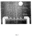
- Fig.1 there is shown schematically a novel apparatus for the detection of DNA in biological samples in accordance with an embodiment of the present invention.
- the chip comprises a silicon wafer 1 on which a layer 2 of aluminum is fabricated, and a layer of aluminum oxide 3 is formed on the aluminum layer 2.
- the aluminum oxide layer 3 is the attachment surface for the DNA probes as will be described below.
- the aluminum oxide layer 3 may be formed either by oxidization of the aluminum layer, or by direct deposition of alumina on the surface of the chip without the need for an aluminum layer at all. These possibilities will be now be described in more detail.
- a first method of forming the aluminum oxide layer aluminum is allowed to grow on a clean aluminum surface that is exposed to oxygen and water.
- Silica chips that are fabricated with a layer of aluminum on the surface are first rinsed with distilled water, cleaned by dipping into 5% (w/v) NaOH solution for about 30s, and then washed several times with distilled water according to the technique described in Sharma CP & Sunny MC "Albumin adsorption on to aluminum oxide and polyurethane surfaces" Biomaterials, 1990; 11: 255-257 .
- the chips are then heated overnight at 37°C in an oven with some water in a container to maintain moisture. Under these conditions the surface of the aluminum oxidizes to alumina with a thickness of about 50 ⁇ .
- the chips may be simply cleaned with distilled water and then heated at 60°C for 48 hours.
- the alumina-coated chip may be patterned by conventional photolithographic techniques. In addition, whichever method is used to form the alumina layer, prior to hybridization the coated chip is washed once with 1x PBS (phosphate-buffered saline, pH 7.4) at room temperature by pipeting the solution repeatedly over the chip surface. Of the alternative methods of forming the alumina layer, sputtering may be preferred as studies show that is produces the lowest background signal. Whichever technique is used for forming the aluminum layer, the thickness may be at least 50 ⁇ .
- Aluminum oxide is preferred for the probe attachment surface because compared with, for example, agarose it is cheaper, more stable and more durable. In addition aluminum oxide can be stored dry and at room temperature. Importantly, aluminum oxide also eliminates the problems associated with electrolysis. In addition, while agarose is difficult to handle to form controlled layers, the pore size and thickness of the alumina layer can easily be controlled (for example by altering the sputtering conditions or the air moisture content). The aluminum oxide can also easily be patterned using conventional photolithographic techniques. The use of a patterned aluminum oxide layer is advantageous because it can reduce the background signal due to reduced non-specific binding, and by increasing the contrast between the area being imaged by the detector and the background.
- the attachment surface is a layer of aluminum oxide formed on aluminum.
- a circular reaction well may be defined by depositing silicon oxide on the aluminum oxide attachment surface.
- capture probes are attached to the aluminum oxide layer.
- the capture probes are not attached directly, however, but through a linkage formed of digoxigenin (DIG) and anti-digoxigenin (anti-DIG) antibodies.
- DIG digoxigenin
- anti-DIG antibodies are adsorbed by the aluminum oxide surface, and the capture probes are formed with a DIG-label whereby the capture probes may be linked via the anti-DIG antibodies to the aluminum oxide attachment surface.
- the aluminum oxide surface is very porous and has the ability to bind many different molecules.
- the anti-DIG coating functions as an attachment layer to ensure that the immobilized DNA capture probes are correctly oriented. If no coating were applied, there is a danger that the detection probe (to be described below) could bind to the aluminum oxide surface and cause interference in the detection of target DNA. In addition, if no coating were applied, the capture probe might bind to the aluminum oxide in the incorrect orientation.
- the anti-DIG/DIG linkage could be replaced by any similar pair of compounds, e.g. an antibody and a target protein, or a pair of proteins with very high affinity for each other, or any pair of non-protein molecules that are able to interact with each other.
- the order of the antibody/protein or protein/protein linkage could be reversed.
- anti-DIG is used as the reactivity limiting coating and the capture probes are DIG-labeled this could be reversed.
- the capture probe could be directly attached to the aluminum oxide layer by the addition of a terminal amine or aldehyde group.
- the capture probes are formed with a DNA sequence complementary to the DNA target that is to be detected in a sample. Therefore, when the sample is supplied to the surface of the chip to which the capture probes are attached, if the target DNA is present it will bind to the complementary DNA sequence of the capture probe by the known process of DNA hybridization.
- the hybridization may preferably be accelerated by the application of an electric current as is known in the art.
- the detection probes include DNA sequences that are complementary to the target DNA and thus will bind to any target DNA that has previously been caught by the capture probes.
- gold nanoparticles coated with streptavidin are added and because of the affinity of streptavidin with biotin the gold nanoparticles will become attached to the detection probes.
- the gold nanoparticles themselves are too small to be seen clearly, but a solution containing silver ions may then be added which will be reduced on the surface of the streptavidin-coated gold nanoparticles to form a silver layer, which is visible as a dark deposit.
- the chip may preferably be treated with salmon sperm DNA.
- salmon sperm DNA As an alternative to salmon sperm DNA, albumin, or other proteins, or Ficoll, may be used.
- the visibility of the silver deposits may be further enhanced by the use of a fixative solution, such as sodium thiosulfate.
- a fixative solution such as sodium thiosulfate.
- Conventional imaging equipment and techniques may then be used to detect dark deposits in the reaction cell, which would result from the presence of the target DNA in the sample.
- the following example is of a protocol for detecting ⁇ -actin DNA in a sample.
- the hybridization steps are electronically assisted, preferably by pulse hybridization using applied pulses, though continuously applied current is also possible. Pulse hybridization, however, limits damage to the chip and results in a higher signal.
- Typical hybridization conditions include for the hybridization of the sample DNA to the capture probes the application of 10 second pulses (13 microamps) followed by a 3 second pause repeated for 8 minutes (i.e. a total of 48 pulses.
- the same conditions may be used, but for only 3 minutes (i.e. 18 pulses).
- the basic DNA detection scheme is the following: an aluminum oxide attachment layer provided with anti-DIG, DIG-labeled capture probes having a DNA fragment complementary to a single-stranded nucleic acid target, biotin-labeled detection probes for binding to captured targets, and streptavidin-coated gold nanoparticles with silver enhancement for visualizing detected target DNA.
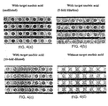
- Figs.2(a)-(d) illustrate the effectiveness of the DIG-labeled capture probe in the detection of the DNA target.
- Figs.2(a) and (c) both show the chip before hybridization. The reaction cells are white because no silver deposits have been formed.
- Figs.2(b) and (d) show the chip after hybridization with the DIG-labeled capture probe being present in Fig.2(b) but absent in Fig.2(d) .
- the reaction cells are seen to be darker in Fig.2(b) than in Fig.2(d) showing the deposit of silver.
- Figs.3(a)-(d) show that darkened silver deposits are only formed in the reaction cells in the presence of the target DNA. Similar to Fig.2 , Figs.3(a) and (c) show the chip before hybridization, while Figs.3(b) and (d) show the chip after hybridization with the target DNA being present in Fig.3(b) only and not Fig.3(d) . Again it can be seen that dark deposits of silver are formed in the reaction cells only in the case of Fig.3(b) where the target DNA is present.
- Figs.4(a)-(d) further demonstrate the effectiveness of the present invention by demonstrating that the silver deposits become darker with increasing target DNA concentration and thus that the optical signal increases in proportion to the target DNA concentration.
- Figs.4(a)-(c) show the chip after hybridization and detection with (a) undiluted target DNA, (b) target DNA diluted 5-fold, and (c) target DNA diluted 10-fold. It will be observed that the reaction cells in Fig.4(a) are darker than those in Fig.4(b) which in turn are darker than those in Fig.4(c).
- Fig.4(d) for comparison shows the chip with no target DNA present and thus white reaction cells with no silver deposited.
- Fig.5 shows that the intensity of the optical signal varies with the concentration of the DIG-capture probe.
- the DIG-capture probe concentration varies decreases from left to right and the reaction cells become correspondingly lighter as less silver is deposited.
Abstract
Description
- This invention relates to apparatus and methods for detecting DNA in biological samples. In particular the present invention relates to novel apparatus for detecting DNA sequences using electrically-assisted nucleic acid hybridization and to methods for optimizing the performance of such apparatus.
- The use of electrically-assisted nucleic acid hybridization is a known technique in the analysis of biological samples containing DNA, e.g. blood, plasma, urine etc. Conventionally, a chip for DNA detection is formed from one of a variety of materials including glass, silica and metal. On the surface of the chip a number of electrical contacts are formed using known techniques. To detect a particular DNA sequence in a biological sample, capture probes consisting of complementary DNA fragments are attached to the chip surface. If a biological sample contains the target DNA, the target DNA will bind to the complementary DNA fragments by hybridization, and various imaging techniques may be used to detect such hybridization and thus the presence in the sample of the target DNA. By applying an electric current to the capture probes, the hybridization process may be accelerated and thus the detection process is also accelerated. This basic hybridization technique is described, for example, in
US 5849486 . - In such devices and techniques, the major issues concerned are the binding of the capture probes to the surface of the chip, and the imaging and visualization of the hybridization when it occurs. Concerning the latter, a traditional method of detection is fluorescence, but more recently Taton et el, ("Science" Vol. 289, 8 September 2000, pp1757-1760) describes the use of streptavidin-coated gold nanoparticles for detection. In such a technique gold nanoparticles are coated with an oligonucleotide sequence complementary to the target DNA sequence. A solution containing such coated gold nanoparticles is passed over the surface of the chip and gold particles will then bind to any probes to which the target DNA is bound. The gold particles themselves are too small to be detected, but the chip surface may then be incubated with a solution containing silver ions. The silver ions are deposited onto the surface of the gold nanoparticles to form a visible silver layer, which may be detected by conventional imaging apparatus.
- Concerning the binding of the capture probes to the chip surface, one difficulty is that the attachment of the DNA oligonucleotides onto a chip surface (e.g. a silicon wafer) is a critical step that is highly sensitive to disturbances in experimental conditions. In particular when an electric current is applied during the electrically assisted hybridization process, electrolysis may occur that can adversely affect subsequent reactions and detection. It is known for example to coat the chip surface with an agarose gel and the DNA oligonucleotides used as capture probes are labeled at one end with biotin and embedded in the agarose layer by virtue of the high affinity interaction between biotin and streptavidin that is dissolved in the agarose prior to the coating of the chip surface.
- However, there are a number of problems with using agarose. Firstly it is very difficult to manipulate a molten agarose gel so as to maintain an even coating on the chip. In addition the density and concentration of the agarose gel must be precisely controlled. Thus manufacture of a chip with a suitable agarose layer is very difficult. Furthermore once applied the gel must be kept moist to prevent drying and cracking, and agarose is very unstable and degrades at high temperatures, and so the chip must be refrigerated after application of the agarose layer. The agarose layer is also very delicate and susceptible to mechanical stresses, and thus the storage and transportation of the finished chip is difficult. In any event, the use of an agarose gel does not overcome the potential problems caused by electrolysis.
- According to a first aspect of the present invention there is provided apparatus for detecting target DNA in a biological sample using electrical hybridization, comprising a substrate formed with at least one reaction cell having an aluminium oxide layer providing a surface on which DNA capture probes are attached; and means for in-use electrically assisted hybridization between said target DNA and said capture probes.
- By means of this arrangement some of the problems with the prior art are overcome or at least mitigated because aluminum oxide provides a stable attachment surface that is easy to form and to manipulate, facilitates subsequent handling and storage of the apparatus, and which overcomes or at least mitigates the problems with electrolysis.
- The aluminum oxide attachment surface may be formed by oxidation of a previously formed aluminum layer, or correctly, for example by sputtering.
- A method of attaching the capture probes to the aluminum oxide layer would increase the convenience of manufacture. An attachment layer adsorbed to the aluminum oxide would perform this function. It is also important to be able to correctly orient the capture probes with respect to the attachment layer. A protein may perform both of these activities.
- Preferably this protein may be an antibody to a protein used to label the DNA capture probes, so that the capture probes may be linked to the attachment surface through an antibody- protein pair linkage in a defined orientation. Alternatively, however, the surface could be coated with any protein and the capture probes may be labeled with a protein having a high affinity with the first protein, for example streptavidin and/or biotin.
- To reduce the background signal, the attachment surface may be coated with a reagent such as albumin, salmon sperm DNA, Ficoll, or other protein. Viewed from a still further aspect the invention also extends to a method of detecting target DNA in a biological sample, comprising the steps of the following:
- (a) providing a reaction cell formed with an aluminum oxide surface being coated with a first compound to ensure the correct orientation of capture probe,
- (b) adding to said cell a solution containing capture probes formed with a DNA sequence complementary to said target DNA and labeled with a second compound having high affinity with said first compound,
- (c) supplying said sample to said cell,
- (d) adding to said cell a solution containing target DNA detection probes formed with a DNA sequence complementary to said target DNA for electrical hybridization with the target DNA,
- (e) providing an electric current for in-use electrically assisted hybridization between said target DNA and said capture probes;
- (f) adding to said cell means for generating a detectable signal in a cell where target DNA has been captured by said capture probes and detected by said detection probes, and
- (g) detecting said signal.
- Viewed from a still further aspect the present invention provides a DNA chip for detecting target DNA in a sample using electrical hybridization, comprising a substrate including at least one reaction cell, said at least one reaction cell having an aluminium oxide layer with a surface on which DNA capture probes are attachable, and means for in-use electrically assisted hybridization between said target and said capture probes whereby said hybridization is accelerated and performance of the apparatus to detect the target DNA is optimized.
- Some embodiments of the present invention will now be described by way of example and with reference to the accompanying drawings, in which:-
-
Fig.1 is a schematic view illustrating a chip according to an embodiment of the invention and also illustrating the hybridization and detection scheme, -
Figs. 2 (a) to (d) show reaction cells obtained experimentally that show that the presence of the capture probe enables the target DNA to be detected, -
Figs. 3 (a) to (d) show reaction cells obtained experimentally that show that the presence of the target DNA is required before silver deposits will be formed, -
Figs. 4 (a) to (d) show reaction cells obtained experimentally that show that the intensity of the silver deposits increases with increasing concentration of the target DNA in the sample, and -
Fig 5 shows reaction cells obtained experimentally that show that the intensity of the silver deposits varies with the concentration of the capture probe. - Referring firstly to
Fig.1 there is shown schematically a novel apparatus for the detection of DNA in biological samples in accordance with an embodiment of the present invention. The chip comprises a silicon wafer 1 on which a layer 2 of aluminum is fabricated, and a layer of aluminum oxide 3 is formed on the aluminum layer 2. The aluminum oxide layer 3 is the attachment surface for the DNA probes as will be described below. - The aluminum oxide layer 3 may be formed either by oxidization of the aluminum layer, or by direct deposition of alumina on the surface of the chip without the need for an aluminum layer at all. These possibilities will be now be described in more detail.
- In a first method of forming the aluminum oxide layer, aluminum is allowed to grow on a clean aluminum surface that is exposed to oxygen and water. Silica chips that are fabricated with a layer of aluminum on the surface are first rinsed with distilled water, cleaned by dipping into 5% (w/v) NaOH solution for about 30s, and then washed several times with distilled water according to the technique described in Sharma CP & Sunny MC "Albumin adsorption on to aluminum oxide and polyurethane surfaces" Biomaterials, 1990; 11: 255-257. The chips are then heated overnight at 37°C in an oven with some water in a container to maintain moisture. Under these conditions the surface of the aluminum oxidizes to alumina with a thickness of about 50Å. In a modification of this process the chips may be simply cleaned with distilled water and then heated at 60°C for 48 hours.
- As an alternative to forming alumina by oxidation of an aluminum layer, alumina may be deposited directly on a silicon wafer according to the following sputtering conditions:
Equipment: ARC-12M Sputtering system RF power: 120W Base pressure: 1.04 x 10⁻⁵ torr Process pressure: 5 x 10⁻³ torr Gas flow: Ar/O2 = 30.2/7.5 sccm Stage rotation: 8 rpm Sputter time: 45 minutes Minimum thickness: 100Å Chip size: 5mm x 5mm - The alumina-coated chip may be patterned by conventional photolithographic techniques. In addition, whichever method is used to form the alumina layer, prior to hybridization the coated chip is washed once with 1x PBS (phosphate-buffered saline, pH 7.4) at room temperature by pipeting the solution repeatedly over the chip surface. Of the alternative methods of forming the alumina layer, sputtering may be preferred as studies show that is produces the lowest background signal. Whichever technique is used for forming the aluminum layer, the thickness may be at least 50Å.
- Aluminum oxide is preferred for the probe attachment surface because compared with, for example, agarose it is cheaper, more stable and more durable. In addition aluminum oxide can be stored dry and at room temperature. Importantly, aluminum oxide also eliminates the problems associated with electrolysis. In addition, while agarose is difficult to handle to form controlled layers, the pore size and thickness of the alumina layer can easily be controlled (for example by altering the sputtering conditions or the air moisture content). The aluminum oxide can also easily be patterned using conventional photolithographic techniques. The use of a patterned aluminum oxide layer is advantageous because it can reduce the background signal due to reduced non-specific binding, and by increasing the contrast between the area being imaged by the detector and the background.
- Referring back to
Fig.1 there is also shown schematically the basic hybridization scheme using an apparatus and method according to an embodiment of the present invention. In particular, inFig.1 the attachment surface is a layer of aluminum oxide formed on aluminum. A circular reaction well may be defined by depositing silicon oxide on the aluminum oxide attachment surface. Within each reaction well, capture probes are attached to the aluminum oxide layer. The capture probes are not attached directly, however, but through a linkage formed of digoxigenin (DIG) and anti-digoxigenin (anti-DIG) antibodies. In particular, anti-DIG antibodies are adsorbed by the aluminum oxide surface, and the capture probes are formed with a DIG-label whereby the capture probes may be linked via the anti-DIG antibodies to the aluminum oxide attachment surface. The aluminum oxide surface is very porous and has the ability to bind many different molecules. The anti-DIG coating functions as an attachment layer to ensure that the immobilized DNA capture probes are correctly oriented. If no coating were applied, there is a danger that the detection probe (to be described below) could bind to the aluminum oxide surface and cause interference in the detection of target DNA. In addition, if no coating were applied, the capture probe might bind to the aluminum oxide in the incorrect orientation. In principle, the anti-DIG/DIG linkage could be replaced by any similar pair of compounds, e.g. an antibody and a target protein, or a pair of proteins with very high affinity for each other, or any pair of non-protein molecules that are able to interact with each other. It should also be understood that the order of the antibody/protein or protein/protein linkage could be reversed. For example while in the preferred embodiment described herein anti-DIG is used as the reactivity limiting coating and the capture probes are DIG-labeled this could be reversed. However, in practical terms it is easier to attach a small molecule such as DIG to a capture probe than it would be to attach an antibody to the capture probe. Furthermore it should be noted that the capture probe could be directly attached to the aluminum oxide layer by the addition of a terminal amine or aldehyde group. - It will also be understood that the capture probes are formed with a DNA sequence complementary to the DNA target that is to be detected in a sample. Therefore, when the sample is supplied to the surface of the chip to which the capture probes are attached, if the target DNA is present it will bind to the complementary DNA sequence of the capture probe by the known process of DNA hybridization. The hybridization may preferably be accelerated by the application of an electric current as is known in the art.
- Once the sample has been applied to the chip surface, it is then necessary to detect any target DNA from the sample that has become bound to the capture probes. To achieve this a solution containing biotinylated detection probes is added. The detection probes include DNA sequences that are complementary to the target DNA and thus will bind to any target DNA that has previously been caught by the capture probes. To enable the caught target DNA to be visually detected, gold nanoparticles coated with streptavidin are added and because of the affinity of streptavidin with biotin the gold nanoparticles will become attached to the detection probes. The gold nanoparticles themselves are too small to be seen clearly, but a solution containing silver ions may then be added which will be reduced on the surface of the streptavidin-coated gold nanoparticles to form a silver layer, which is visible as a dark deposit.
- To reduce the background signal the chip may preferably be treated with salmon sperm DNA. As an alternative to salmon sperm DNA, albumin, or other proteins, or Ficoll, may be used.
- The visibility of the silver deposits may be further enhanced by the use of a fixative solution, such as sodium thiosulfate. Conventional imaging equipment and techniques may then be used to detect dark deposits in the reaction cell, which would result from the presence of the target DNA in the sample.
- The following example is of a protocol for detecting β-actin DNA in a sample. The hybridization steps are electronically assisted, preferably by pulse hybridization using applied pulses, though continuously applied current is also possible. Pulse hybridization, however, limits damage to the chip and results in a higher signal. Typical hybridization conditions include for the hybridization of the sample DNA to the capture probes the application of 10 second pulses (13 microamps) followed by a 3 second pause repeated for 8 minutes (i.e. a total of 48 pulses. For the hybridization of the detection probe to the captured sample DNA, the same conditions may be used, but for only 3 minutes (i.e. 18 pulses).
- 1. Anti-DIG is diluted 100-fold with 1x PBS (phosphate-buffered saline), pH 7.4.
- 2. 50µl of the diluted anti-DIG is added onto an alumina-coated chip and is incubated at 41°C for 2 hours.
- 3. The anti-DIG solution is discarded and the chip is washed 3x with 80µl 1x PBS, pH 7.4 (pipette up and down during every wash).
- 4. 1µl 10µM of the DIG-labeled capture probes together with 0.2µg salmon sperm DNA in 50µl 1x PBS is added onto the chip and incubated at 41°C for 30 minutes. The salmon sperm DNA is firstly denatured by heating to 95°C to form single strands and is then mixed with the DIG-labeled capture probes.
- 5. The DIG-labeled capture probe solution and salmon sperm DNA solution are discarded washed three times with 80µl 1x PBS and once with 1x SSPE.
- 6. Add 5µl 11µM sample of β-actin sequence (a 91 nucleotide single-stranded target) in 1x SSPE and apply electric pulse current as described for 8 min. After hybridization, wash the chip 3x with 0.1x SSPE.
- 7. Add detection probe (1ul, 10µM) to the chip. Apply electric pulse current as described for 3 min. Wash the chip 3x with 0.1x SSPE and once with 1x PBS.
- 8. Streptavidin-coated gold nanoparticles (obtained from Sigma Chemical Co., Ltd, St. Louis, Missouri, USA) are diluted 10-fold with 1x PBS, pH 7.4.
- 9. The diluted streptavidin-coated gold nanoparticles are added to the chip surface and incubated at 41°C for 15 minutes.
- 10. The diluted streptavidin-coated gold nanoparticle solution is discarded and the chip is washed twice with 80µl 1x PBS, pH 7.4 (pipette up and down during every wash) and 3x with 80µl autoclaved milli-Q water (pipette up and down during every wash).
- 11. A 1:1 mixture of silver enhancer solutions A and B (obtained from Sigma Chemical Co., Ltd, St. Louis, Missouri, USA) is prepared just before use and the following steps are performed in a darkroom. 50µl of the silver enhancer solution is added onto the chip and incubated at room temperature for 5 minutes.
- 12. The silver enhancer solution is discarded and the chip washed once with autoclaved milli-Q water before 50µl of 2% sodium thiosulfate is added onto the chip. Pipette up and down once to remove background and to fix the color.
- 13. Discard the sodium thiosulfate solution after 2 min incubation and washed with 50µl milli-Q water before 50µl autoclaved milli-Q water is added onto the chip.
- 14. Observe the appearance of dark spots on the chip with an optical signal detection system.
- The following experimental results shown in
Figs.2 to 5 were obtained using the above hybridization protocol with certain parameters being varied as will be understood from the following. In all cases, the basic DNA detection scheme is the following: an aluminum oxide attachment layer provided with anti-DIG, DIG-labeled capture probes having a DNA fragment complementary to a single-stranded nucleic acid target, biotin-labeled detection probes for binding to captured targets, and streptavidin-coated gold nanoparticles with silver enhancement for visualizing detected target DNA. -
Figs.2(a)-(d) illustrate the effectiveness of the DIG-labeled capture probe in the detection of the DNA target.Figs.2(a) and (c) both show the chip before hybridization. The reaction cells are white because no silver deposits have been formed.Figs.2(b) and (d) show the chip after hybridization with the DIG-labeled capture probe being present inFig.2(b) but absent inFig.2(d) . The reaction cells are seen to be darker inFig.2(b) than inFig.2(d) showing the deposit of silver. -
Figs.3(a)-(d) show that darkened silver deposits are only formed in the reaction cells in the presence of the target DNA. Similar toFig.2 ,Figs.3(a) and (c) show the chip before hybridization, whileFigs.3(b) and (d) show the chip after hybridization with the target DNA being present inFig.3(b) only and notFig.3(d) . Again it can be seen that dark deposits of silver are formed in the reaction cells only in the case ofFig.3(b) where the target DNA is present. -
Figs.4(a)-(d) further demonstrate the effectiveness of the present invention by demonstrating that the silver deposits become darker with increasing target DNA concentration and thus that the optical signal increases in proportion to the target DNA concentration.Figs.4(a)-(c) show the chip after hybridization and detection with (a) undiluted target DNA, (b) target DNA diluted 5-fold, and (c) target DNA diluted 10-fold. It will be observed that the reaction cells inFig.4(a) are darker than those inFig.4(b) which in turn are darker than those inFig.4(c). Fig.4(d) for comparison shows the chip with no target DNA present and thus white reaction cells with no silver deposited. - Finally,
Fig.5 shows that the intensity of the optical signal varies with the concentration of the DIG-capture probe. InFig.5 the DIG-capture probe concentration varies decreases from left to right and the reaction cells become correspondingly lighter as less silver is deposited.
Claims (24)
- Apparatus for detecting target DNA in a biological sample using electrical hybridization, comprising a substrate formed with at least one reaction cell having an aluminium oxide layer providing a surface on which DNA capture probes are attached; and means for in-use electrically assisted hybridization between said target DNA and said capture probes.
- Apparatus as claimed in claim 1 wherein said aluminum oxide surface is formed by oxidation of an aluminum layer.
- Apparatus as claimed in claim 1 wherein said aluminum oxide surface is formed by a sputtering technique.
- Apparatus as claimed in any of claims 1-3 wherein said aluminum oxide surface is coated with a first compound to act as attachment layer for the capture probe.
- Apparatus as claimed in claim 4 wherein said apparatus further comprises capture probes attached to said aluminum oxide surface, and wherein said capture probes are labeled with a second compound which can attach to the said first compound.
- Apparatus as claimed in claim 5 wherein said first and second compounds comprise an antibody-protein pair.
- Apparatus as claimed in claim 6 wherein said first compound comprises anti-digoxigenin antibodies, and wherein said second compound comprises digoxigenin.
- Apparatus as claimed in claim 5 wherein said first and second compounds comprise streptavidin and biotin, or vice versa.
- Apparatus as claimed in any of claim 1-3 wherein said aluminum oxide surface is coated with a first molecule to act as an attachment layer for the capture probe.
- Apparatus as claimed in claim 9 wherein said apparatus further comprises capture probes attached to said aluminum oxide surface, and wherein said capture probes are labeled with a second molecule having an affinity with said first molecule.
- Apparatus as claimed in any of claims 1-10 wherein said aluminum oxide layer has a thickness of at least 50Å.
- Apparatus as claimed in any of claims 1-11 wherein said aluminum oxide surface is coated with a reagent to reduce the background signal in a detection process.
- Apparatus as claimed in claim 12 wherein said reagent comprises salmon sperm DNA.
- Apparatus as claimed in claim 12 wherein said reagent comprises albumin, or other protein, or Ficoll.
- A method of detecting target DNA in a biological sample, comprising the steps of the following:(a) providing a reaction cell being free of any agarose or gel layer and formed with an aluminum oxide surface being coated with a first compound to ensure the correct orientation of capture probe,(b) adding to said cell a solution containing capture probes formed with a DNA sequence complementary to said target DNA and labeled with a second compound having high affinity with said first compound,(c) supplying said sample to said cell,(d) adding to said cell a solution containing target DNA detection probes formed with a DNA sequence complementary to said target DNA for electrical hybridization with the target DNA,(e) providing an electric current for in-use electrically assisted hybridization between said target DNA and said capture probes;(f) adding to said cell means for generating a detectable signal in a cell where target DNA has been captured by said capture probes and detected by said detection probes, and(g) detecting said signal.
- A method as claimed in claim 15 wherein said first and second compound comprise an antibody-protein pair.
- A method as claimed in claim 16 wherein said first and second compound comprise ahti-digoxigenin and digoxigenin.
- A method as claimed in cairn 16 wherein said first and second compound comprise an interacting pair of proteins or non-protein molecules with affinity for one another.
- A method as claimed in claim 16 wherein said first and second compound comprise streptavidin and biotin, or vice versa.
- A method as claimed in any of claims 15-19 further comprising the addition of a reagent for reducing the background signal.
- A method as claimed in claim 20 wherein said background signal reducing reagent is albumin or is derived from salmon sperm DNA.
- A method as claimed in any of claims 15-21 wherein in step (f) said means for generating said signal includes a solution of streptavidin-coated gold nanoparticles that bind to said detection probe, and a solution of silver ions that are reduced on the surface of said gold nanoparticles to form silver deposits.
- A DNA chip for detecting target DNA in a sample using electrical hybridization, comprising a substrate including at least one reaction cell, said at least one reaction cell having an aluminium oxide layer with a surface on which DNA capture probes are attachable, and means for in-use electrically assisted hybridization between said target and said capture probes.
- A method as claimed in claim 23 wherein said electric current is a pulsed electric current.
Applications Claiming Priority (3)
| Application Number | Priority Date | Filing Date | Title |
|---|---|---|---|
| US216928 | 2002-08-13 | ||
| US10/216,928 US7153687B2 (en) | 2002-08-13 | 2002-08-13 | Apparatus and methods for detecting DNA in biological samples |
| PCT/CN2003/000661 WO2004015138A1 (en) | 2002-08-13 | 2003-08-12 | Apparatus and methods for detecting dna in biological samples |
Publications (3)
| Publication Number | Publication Date |
|---|---|
| EP1552017A1 EP1552017A1 (en) | 2005-07-13 |
| EP1552017A4 EP1552017A4 (en) | 2007-08-29 |
| EP1552017B1 true EP1552017B1 (en) | 2010-02-17 |
Family
ID=31714337
Family Applications (1)
| Application Number | Title | Priority Date | Filing Date |
|---|---|---|---|
| EP03783907A Expired - Lifetime EP1552017B1 (en) | 2002-08-13 | 2003-08-12 | Apparatus and methods for detecting dna in biological samples |
Country Status (16)
| Country | Link |
|---|---|
| US (4) | US7153687B2 (en) |
| EP (1) | EP1552017B1 (en) |
| JP (2) | JP4914006B2 (en) |
| KR (1) | KR101075760B1 (en) |
| CN (2) | CN2611383Y (en) |
| AT (1) | ATE458069T1 (en) |
| AU (1) | AU2003257367B2 (en) |
| BR (1) | BR0313409A (en) |
| CA (1) | CA2495520C (en) |
| DE (1) | DE60331335D1 (en) |
| DK (1) | DK1552017T3 (en) |
| ES (1) | ES2339008T3 (en) |
| HK (1) | HK1082771A1 (en) |
| PT (1) | PT1552017E (en) |
| SG (1) | SG153659A1 (en) |
| WO (1) | WO2004015138A1 (en) |
Families Citing this family (13)
| Publication number | Priority date | Publication date | Assignee | Title |
|---|---|---|---|---|
| JP2003322654A (en) * | 2002-02-27 | 2003-11-14 | Hitachi Software Eng Co Ltd | Biopolymer detecting method |
| US9388459B2 (en) * | 2002-06-17 | 2016-07-12 | Affymetrix, Inc. | Methods for genotyping |
| US7153687B2 (en) * | 2002-08-13 | 2006-12-26 | Hong Kong Dna Chips Limited | Apparatus and methods for detecting DNA in biological samples |
| US7390622B2 (en) * | 2003-10-16 | 2008-06-24 | Hai Kang Life Corporation Limited | Apparatus and methods for detecting nucleic acid in biological samples |
| US8906609B1 (en) | 2005-09-26 | 2014-12-09 | Arrowhead Center, Inc. | Label-free biomolecule sensor based on surface charge modulated ionic conductance |
| KR100724093B1 (en) * | 2005-11-14 | 2007-06-04 | 한국표준과학연구원 | DNA detection method using the Au-DNA aggregates |
| US11306351B2 (en) | 2005-12-21 | 2022-04-19 | Affymetrix, Inc. | Methods for genotyping |
| US20120322064A1 (en) * | 2011-05-23 | 2012-12-20 | Board Of Trustees Of Michigan State University | Hybridization probes and methods of their use |
| US10030241B2 (en) | 2015-03-30 | 2018-07-24 | General Electric Company | Methods and kits for capturing sperm nucleic acids |
| US9957548B2 (en) | 2015-03-30 | 2018-05-01 | General Electric Company | Methods of capturing sperm nucleic acids |
| US10379101B2 (en) * | 2015-11-23 | 2019-08-13 | Hai Kang Life Corporation Limited | Apparatus for detection of biomolecules and its fabrication |
| CN106198952A (en) * | 2016-07-01 | 2016-12-07 | 清华大学 | A kind of suppress the nucleic acid molecules enclosure method to sensing interface non-specific adsorption |
| GB2552461B (en) * | 2016-07-14 | 2022-06-15 | Rightangled Ltd | Method and assay kit to detect an analyte |
Family Cites Families (23)
| Publication number | Priority date | Publication date | Assignee | Title |
|---|---|---|---|---|
| US5162229A (en) * | 1988-03-15 | 1992-11-10 | Akzo N.V. | Device and method for enhanced recovery and detection of microbial growth in the presence of antimicrobial substances |
| AU5126890A (en) * | 1989-04-03 | 1990-10-04 | Minnesota Mining And Manufacturing Company | Metal oxide supports for nucleic acids |
| US5128247A (en) * | 1989-08-14 | 1992-07-07 | Board Of Regents, The University Of Texas System | Methods for isolation of nucleic acids from eukaryotic and prokaryotic sources |
| US5632957A (en) * | 1993-11-01 | 1997-05-27 | Nanogen | Molecular biological diagnostic systems including electrodes |
| US5849486A (en) * | 1993-11-01 | 1998-12-15 | Nanogen, Inc. | Methods for hybridization analysis utilizing electrically controlled hybridization |
| US6017696A (en) | 1993-11-01 | 2000-01-25 | Nanogen, Inc. | Methods for electronic stringency control for molecular biological analysis and diagnostics |
| US6051380A (en) * | 1993-11-01 | 2000-04-18 | Nanogen, Inc. | Methods and procedures for molecular biological analysis and diagnostics |
| US5605662A (en) | 1993-11-01 | 1997-02-25 | Nanogen, Inc. | Active programmable electronic devices for molecular biological analysis and diagnostics |
| US6287517B1 (en) * | 1993-11-01 | 2001-09-11 | Nanogen, Inc. | Laminated assembly for active bioelectronic devices |
| US6767702B2 (en) | 1996-07-29 | 2004-07-27 | Nanosphere, Inc. | Nanoparticles having oligonucleotides attached thereto and uses therefor |
| US6303338B1 (en) * | 1996-08-16 | 2001-10-16 | Human Genome Sciences, Inc. | Pancreas-derived plasminogen activator inhibitor |
| EP1019711A4 (en) | 1996-09-06 | 2001-06-13 | Nanogen Inc | Methods and materials for optimization of electronic hybridization reactions |
| PT1050588E (en) * | 1997-07-11 | 2005-04-29 | Pamgene Bv | METHOD FOR PRODUCING A DEVICE FOR PERFORMING A TEST, USING A MEMBRANE FOR MANUFACTURING THE REFERENCE DEVICE, A CONTAINER UNDERSTANDING THE DEVICE AND METHOD FOR DETECTING AN ANALYST USING THAT DEVICE |
| US6123819A (en) * | 1997-11-12 | 2000-09-26 | Protiveris, Inc. | Nanoelectrode arrays |
| US6093370A (en) * | 1998-06-11 | 2000-07-25 | Hitachi, Ltd. | Polynucleotide separation method and apparatus therefor |
| JP2001178470A (en) * | 1999-12-27 | 2001-07-03 | Fuji Photo Film Co Ltd | Method for immobilizing dna fragment to surface of solid- phase carrier and dna chip |
| EP1967595A3 (en) * | 2000-02-16 | 2008-12-03 | Illumina, Inc. | Parallel genotyping of multiple patient samples |
| ATE487136T1 (en) | 2000-03-28 | 2010-11-15 | Nanosphere Inc | NANOPARTICLES WITH BONDED OLIGONUCLEOTIDES AND USES THEREOF |
| CA2407973C (en) | 2000-05-03 | 2011-06-07 | Jen-Jr Gau | Biological identification system with integrated sensor chip |
| EP1362121A2 (en) | 2000-08-11 | 2003-11-19 | Nanosphere, Inc. | Nanoparticles having oligonucleotides attached thereto and uses therefor |
| US6942970B2 (en) * | 2000-09-14 | 2005-09-13 | Zymed Laboratories, Inc. | Identifying subjects suitable for topoisomerase II inhibitor treatment |
| AU2002230593A1 (en) | 2000-12-08 | 2002-06-18 | Nanosphere, Inc. | Nanoparticles having oligonucleotides attached thereto and uses therefor |
| US7153687B2 (en) * | 2002-08-13 | 2006-12-26 | Hong Kong Dna Chips Limited | Apparatus and methods for detecting DNA in biological samples |
-
2002
- 2002-08-13 US US10/216,928 patent/US7153687B2/en not_active Expired - Fee Related
- 2002-10-24 CN CNU022820833U patent/CN2611383Y/en not_active Expired - Lifetime
-
2003
- 2003-08-12 WO PCT/CN2003/000661 patent/WO2004015138A1/en active Application Filing
- 2003-08-12 CA CA2495520A patent/CA2495520C/en not_active Expired - Fee Related
- 2003-08-12 ES ES03783907T patent/ES2339008T3/en not_active Expired - Lifetime
- 2003-08-12 AU AU2003257367A patent/AU2003257367B2/en not_active Ceased
- 2003-08-12 EP EP03783907A patent/EP1552017B1/en not_active Expired - Lifetime
- 2003-08-12 DE DE60331335T patent/DE60331335D1/en not_active Expired - Lifetime
- 2003-08-12 PT PT03783907T patent/PT1552017E/en unknown
- 2003-08-12 JP JP2004526591A patent/JP4914006B2/en not_active Expired - Fee Related
- 2003-08-12 KR KR1020057002443A patent/KR101075760B1/en not_active IP Right Cessation
- 2003-08-12 BR BR0313409-1A patent/BR0313409A/en not_active IP Right Cessation
- 2003-08-12 DK DK03783907.3T patent/DK1552017T3/en active
- 2003-08-12 AT AT03783907T patent/ATE458069T1/en not_active IP Right Cessation
- 2003-08-12 SG SG200700913-7A patent/SG153659A1/en unknown
- 2003-08-12 CN CN038194783A patent/CN1675375B/en not_active Expired - Fee Related
-
2006
- 2006-01-12 HK HK06100521.2A patent/HK1082771A1/en not_active IP Right Cessation
- 2006-11-15 US US11/599,479 patent/US7749705B2/en not_active Expired - Fee Related
-
2010
- 2010-05-24 US US12/786,178 patent/US8198070B2/en not_active Expired - Lifetime
-
2011
- 2011-03-16 US US13/049,858 patent/US8110669B2/en not_active Expired - Lifetime
- 2011-09-07 JP JP2011194496A patent/JP2012040009A/en active Pending
Also Published As
| Publication number | Publication date |
|---|---|
| JP2005535319A (en) | 2005-11-24 |
| DE60331335D1 (en) | 2010-04-01 |
| HK1082771A1 (en) | 2006-06-16 |
| ATE458069T1 (en) | 2010-03-15 |
| US20110165665A1 (en) | 2011-07-07 |
| CA2495520C (en) | 2013-06-25 |
| AU2003257367B2 (en) | 2010-11-25 |
| US20100233721A1 (en) | 2010-09-16 |
| AU2003257367A1 (en) | 2004-02-25 |
| US20070065872A1 (en) | 2007-03-22 |
| ES2339008T3 (en) | 2010-05-14 |
| EP1552017A4 (en) | 2007-08-29 |
| JP4914006B2 (en) | 2012-04-11 |
| US7153687B2 (en) | 2006-12-26 |
| CN1675375B (en) | 2013-07-03 |
| KR101075760B1 (en) | 2011-10-24 |
| JP2012040009A (en) | 2012-03-01 |
| PT1552017E (en) | 2010-03-31 |
| US8110669B2 (en) | 2012-02-07 |
| CN1675375A (en) | 2005-09-28 |
| US7749705B2 (en) | 2010-07-06 |
| EP1552017A1 (en) | 2005-07-13 |
| CA2495520A1 (en) | 2004-02-19 |
| WO2004015138A1 (en) | 2004-02-19 |
| US8198070B2 (en) | 2012-06-12 |
| US20040033496A1 (en) | 2004-02-19 |
| CN2611383Y (en) | 2004-04-14 |
| SG153659A1 (en) | 2009-07-29 |
| KR20050053614A (en) | 2005-06-08 |
| BR0313409A (en) | 2005-07-12 |
| DK1552017T3 (en) | 2010-05-31 |
Similar Documents
| Publication | Publication Date | Title |
|---|---|---|
| US8110669B2 (en) | Apparatus and methods for detecting DNA in biological samples | |
| JP3605607B2 (en) | Detection method by enhanced silver staining | |
| EP1075656B1 (en) | Detection of a target in a sample | |
| JP2005516610A (en) | Gene expression analysis using nicking agents | |
| US7645574B2 (en) | Methods of metallizing nucleic acid molecules and methods of attaching nucleic acid molecules to conductive surfaces | |
| US9266726B2 (en) | Method for making biochips | |
| WO2004096986A2 (en) | Method for quantitative detection of nucleic acid molecules | |
| US20030119028A1 (en) | Device and methods for enhanced microarray hybridization reactions | |
| KR20070091608A (en) | Biomolecular recognition of crystal defects | |
| AU2007224397B2 (en) | Apparatus and Methods for Detecting DNA in Biological Samples | |
| US9040251B2 (en) | Biomolecule fixing board and method of manufacturing the same | |
| JPWO2004048973A1 (en) | Immobilization of biomolecules on metal carriers | |
| Zhang et al. | Antibody-and aptamer-free SERS substrate for ultrasensitive and anti-interference detection of SARS-CoV-2 spike protein in untreated saliva | |
| JP2007259867A (en) | Hybridization method utilizing electrostatic transportation and devices therefor |
Legal Events
| Date | Code | Title | Description |
|---|---|---|---|
| PUAI | Public reference made under article 153(3) epc to a published international application that has entered the european phase |
Free format text: ORIGINAL CODE: 0009012 |
|
| 17P | Request for examination filed |
Effective date: 20050207 |
|
| AK | Designated contracting states |
Kind code of ref document: A1 Designated state(s): AT BE BG CH CY CZ DE DK EE ES FI FR GB GR HU IE IT LI LU MC NL PT RO SE SI SK TR |
|
| AX | Request for extension of the european patent |
Extension state: AL LT LV MK |
|
| DAX | Request for extension of the european patent (deleted) | ||
| REG | Reference to a national code |
Ref country code: HK Ref legal event code: DE Ref document number: 1082771 Country of ref document: HK |
|
| RIN1 | Information on inventor provided before grant (corrected) |
Inventor name: CHAN, DUNCAN KA-YUN,ROOM 1816, CHOI PING HOUSE Inventor name: LIN, SELMA, SAU, WAH,UNIT G, 38/F, TOWER 1 Inventor name: LAU, LOK-TING,ROOM 1906, HEUNG TUNG HOUSE Inventor name: YU, CHEUNG HOI,20/F,SUITE E,TOWER 1,THE BELCHER'S |
|
| A4 | Supplementary search report drawn up and despatched |
Effective date: 20070801 |
|
| RAP1 | Party data changed (applicant data changed or rights of an application transferred) |
Owner name: HAI KANG LIFE CORPORATION LIMITED |
|
| 17Q | First examination report despatched |
Effective date: 20080526 |
|
| GRAP | Despatch of communication of intention to grant a patent |
Free format text: ORIGINAL CODE: EPIDOSNIGR1 |
|
| GRAC | Information related to communication of intention to grant a patent modified |
Free format text: ORIGINAL CODE: EPIDOSCIGR1 |
|
| GRAS | Grant fee paid |
Free format text: ORIGINAL CODE: EPIDOSNIGR3 |
|
| GRAA | (expected) grant |
Free format text: ORIGINAL CODE: 0009210 |
|
| AK | Designated contracting states |
Kind code of ref document: B1 Designated state(s): AT BE BG CH CY CZ DE DK EE ES FI FR GB GR HU IE IT LI LU MC NL PT RO SE SI SK TR |
|
| REG | Reference to a national code |
Ref country code: GB Ref legal event code: FG4D |
|
| REG | Reference to a national code |
Ref country code: CH Ref legal event code: EP |
|
| REG | Reference to a national code |
Ref country code: IE Ref legal event code: FG4D |
|
| REG | Reference to a national code |
Ref country code: CH Ref legal event code: NV Representative=s name: SERVOPATENT GMBH Ref country code: PT Ref legal event code: SC4A Free format text: AVAILABILITY OF NATIONAL TRANSLATION Effective date: 20100325 |
|
| REF | Corresponds to: |
Ref document number: 60331335 Country of ref document: DE Date of ref document: 20100401 Kind code of ref document: P |
|
| REG | Reference to a national code |
Ref country code: SE Ref legal event code: TRGR |
|
| REG | Reference to a national code |
Ref country code: NL Ref legal event code: T3 |
|
| REG | Reference to a national code |
Ref country code: ES Ref legal event code: FG2A Ref document number: 2339008 Country of ref document: ES Kind code of ref document: T3 |
|
| REG | Reference to a national code |
Ref country code: DK Ref legal event code: T3 |
|
| REG | Reference to a national code |
Ref country code: GR Ref legal event code: EP Ref document number: 20100401044 Country of ref document: GR |
|
| REG | Reference to a national code |
Ref country code: HK Ref legal event code: GR Ref document number: 1082771 Country of ref document: HK |
|
| PG25 | Lapsed in a contracting state [announced via postgrant information from national office to epo] |
Ref country code: SI Free format text: LAPSE BECAUSE OF FAILURE TO SUBMIT A TRANSLATION OF THE DESCRIPTION OR TO PAY THE FEE WITHIN THE PRESCRIBED TIME-LIMIT Effective date: 20100217 Ref country code: AT Free format text: LAPSE BECAUSE OF FAILURE TO SUBMIT A TRANSLATION OF THE DESCRIPTION OR TO PAY THE FEE WITHIN THE PRESCRIBED TIME-LIMIT Effective date: 20100217 |
|
| PG25 | Lapsed in a contracting state [announced via postgrant information from national office to epo] |
Ref country code: CY Free format text: LAPSE BECAUSE OF FAILURE TO SUBMIT A TRANSLATION OF THE DESCRIPTION OR TO PAY THE FEE WITHIN THE PRESCRIBED TIME-LIMIT Effective date: 20100217 Ref country code: EE Free format text: LAPSE BECAUSE OF FAILURE TO SUBMIT A TRANSLATION OF THE DESCRIPTION OR TO PAY THE FEE WITHIN THE PRESCRIBED TIME-LIMIT Effective date: 20100217 Ref country code: RO Free format text: LAPSE BECAUSE OF FAILURE TO SUBMIT A TRANSLATION OF THE DESCRIPTION OR TO PAY THE FEE WITHIN THE PRESCRIBED TIME-LIMIT Effective date: 20100217 |
|
| PG25 | Lapsed in a contracting state [announced via postgrant information from national office to epo] |
Ref country code: BG Free format text: LAPSE BECAUSE OF FAILURE TO SUBMIT A TRANSLATION OF THE DESCRIPTION OR TO PAY THE FEE WITHIN THE PRESCRIBED TIME-LIMIT Effective date: 20100517 Ref country code: CZ Free format text: LAPSE BECAUSE OF FAILURE TO SUBMIT A TRANSLATION OF THE DESCRIPTION OR TO PAY THE FEE WITHIN THE PRESCRIBED TIME-LIMIT Effective date: 20100217 Ref country code: SK Free format text: LAPSE BECAUSE OF FAILURE TO SUBMIT A TRANSLATION OF THE DESCRIPTION OR TO PAY THE FEE WITHIN THE PRESCRIBED TIME-LIMIT Effective date: 20100217 |
|
| PLBE | No opposition filed within time limit |
Free format text: ORIGINAL CODE: 0009261 |
|
| STAA | Information on the status of an ep patent application or granted ep patent |
Free format text: STATUS: NO OPPOSITION FILED WITHIN TIME LIMIT |
|
| 26N | No opposition filed |
Effective date: 20101118 |
|
| PGFP | Annual fee paid to national office [announced via postgrant information from national office to epo] |
Ref country code: CH Payment date: 20110812 Year of fee payment: 9 Ref country code: DK Payment date: 20110810 Year of fee payment: 9 |
|
| PG25 | Lapsed in a contracting state [announced via postgrant information from national office to epo] |
Ref country code: HU Free format text: LAPSE BECAUSE OF FAILURE TO SUBMIT A TRANSLATION OF THE DESCRIPTION OR TO PAY THE FEE WITHIN THE PRESCRIBED TIME-LIMIT Effective date: 20100818 |
|
| PGFP | Annual fee paid to national office [announced via postgrant information from national office to epo] |
Ref country code: LU Payment date: 20120814 Year of fee payment: 10 |
|
| PGFP | Annual fee paid to national office [announced via postgrant information from national office to epo] |
Ref country code: FI Payment date: 20120810 Year of fee payment: 10 Ref country code: MC Payment date: 20120809 Year of fee payment: 10 Ref country code: SE Payment date: 20120813 Year of fee payment: 10 Ref country code: GB Payment date: 20120808 Year of fee payment: 10 Ref country code: IE Payment date: 20120810 Year of fee payment: 10 |
|
| PGFP | Annual fee paid to national office [announced via postgrant information from national office to epo] |
Ref country code: TR Payment date: 20120801 Year of fee payment: 10 Ref country code: GR Payment date: 20120817 Year of fee payment: 10 |
|
| PGFP | Annual fee paid to national office [announced via postgrant information from national office to epo] |
Ref country code: IT Payment date: 20120814 Year of fee payment: 10 Ref country code: BE Payment date: 20120820 Year of fee payment: 10 Ref country code: ES Payment date: 20120907 Year of fee payment: 10 Ref country code: DE Payment date: 20120808 Year of fee payment: 10 Ref country code: FR Payment date: 20120823 Year of fee payment: 10 |
|
| PGFP | Annual fee paid to national office [announced via postgrant information from national office to epo] |
Ref country code: NL Payment date: 20120809 Year of fee payment: 10 Ref country code: PT Payment date: 20120213 Year of fee payment: 10 |
|
| REG | Reference to a national code |
Ref country code: PT Ref legal event code: MM4A Free format text: LAPSE DUE TO NON-PAYMENT OF FEES Effective date: 20140212 |
|
| BERE | Be: lapsed |
Owner name: HAI KANG LIFE CORPORATION LIMITED Effective date: 20130831 |
|
| REG | Reference to a national code |
Ref country code: NL Ref legal event code: V1 Effective date: 20140301 |
|
| REG | Reference to a national code |
Ref country code: CH Ref legal event code: PL Ref country code: DK Ref legal event code: EBP Effective date: 20130831 |
|
| REG | Reference to a national code |
Ref country code: SE Ref legal event code: EUG |
|
| GBPC | Gb: european patent ceased through non-payment of renewal fee |
Effective date: 20130812 |
|
| REG | Reference to a national code |
Ref country code: GR Ref legal event code: ML Ref document number: 20100401044 Country of ref document: GR Effective date: 20140305 |
|
| PG25 | Lapsed in a contracting state [announced via postgrant information from national office to epo] |
Ref country code: MC Free format text: LAPSE BECAUSE OF NON-PAYMENT OF DUE FEES Effective date: 20130902 Ref country code: FI Free format text: LAPSE BECAUSE OF NON-PAYMENT OF DUE FEES Effective date: 20130812 Ref country code: DE Free format text: LAPSE BECAUSE OF NON-PAYMENT OF DUE FEES Effective date: 20140301 Ref country code: CH Free format text: LAPSE BECAUSE OF NON-PAYMENT OF DUE FEES Effective date: 20130831 Ref country code: NL Free format text: LAPSE BECAUSE OF NON-PAYMENT OF DUE FEES Effective date: 20140301 Ref country code: LI Free format text: LAPSE BECAUSE OF NON-PAYMENT OF DUE FEES Effective date: 20130831 Ref country code: SE Free format text: LAPSE BECAUSE OF NON-PAYMENT OF DUE FEES Effective date: 20130813 |
|
| REG | Reference to a national code |
Ref country code: IE Ref legal event code: MM4A |
|
| REG | Reference to a national code |
Ref country code: DE Ref legal event code: R119 Ref document number: 60331335 Country of ref document: DE Effective date: 20140301 |
|
| REG | Reference to a national code |
Ref country code: FR Ref legal event code: ST Effective date: 20140430 |
|
| PG25 | Lapsed in a contracting state [announced via postgrant information from national office to epo] |
Ref country code: IT Free format text: LAPSE BECAUSE OF NON-PAYMENT OF DUE FEES Effective date: 20130812 Ref country code: GR Free format text: LAPSE BECAUSE OF NON-PAYMENT OF DUE FEES Effective date: 20140305 Ref country code: BE Free format text: LAPSE BECAUSE OF NON-PAYMENT OF DUE FEES Effective date: 20130831 |
|
| PG25 | Lapsed in a contracting state [announced via postgrant information from national office to epo] |
Ref country code: PT Free format text: LAPSE BECAUSE OF NON-PAYMENT OF DUE FEES Effective date: 20140212 |
|
| PG25 | Lapsed in a contracting state [announced via postgrant information from national office to epo] |
Ref country code: GB Free format text: LAPSE BECAUSE OF NON-PAYMENT OF DUE FEES Effective date: 20130812 Ref country code: IE Free format text: LAPSE BECAUSE OF NON-PAYMENT OF DUE FEES Effective date: 20130812 |
|
| PG25 | Lapsed in a contracting state [announced via postgrant information from national office to epo] |
Ref country code: FR Free format text: LAPSE BECAUSE OF NON-PAYMENT OF DUE FEES Effective date: 20130902 |
|
| REG | Reference to a national code |
Ref country code: ES Ref legal event code: FD2A Effective date: 20140905 |
|
| PG25 | Lapsed in a contracting state [announced via postgrant information from national office to epo] |
Ref country code: DK Free format text: LAPSE BECAUSE OF NON-PAYMENT OF DUE FEES Effective date: 20130831 |
|
| PG25 | Lapsed in a contracting state [announced via postgrant information from national office to epo] |
Ref country code: ES Free format text: LAPSE BECAUSE OF NON-PAYMENT OF DUE FEES Effective date: 20130813 |
|
| PG25 | Lapsed in a contracting state [announced via postgrant information from national office to epo] |
Ref country code: LU Free format text: LAPSE BECAUSE OF NON-PAYMENT OF DUE FEES Effective date: 20130812 |
|
| PG25 | Lapsed in a contracting state [announced via postgrant information from national office to epo] |
Ref country code: TR Free format text: LAPSE BECAUSE OF NON-PAYMENT OF DUE FEES Effective date: 20130812 |