EP1548600A1 - Data management device and method for flash memory - Google Patents
Data management device and method for flash memory Download PDFInfo
- Publication number
- EP1548600A1 EP1548600A1 EP04257934A EP04257934A EP1548600A1 EP 1548600 A1 EP1548600 A1 EP 1548600A1 EP 04257934 A EP04257934 A EP 04257934A EP 04257934 A EP04257934 A EP 04257934A EP 1548600 A1 EP1548600 A1 EP 1548600A1
- Authority
- EP
- European Patent Office
- Prior art keywords
- physical
- data
- addresses
- data operation
- logical
- Prior art date
- Legal status (The legal status is an assumption and is not a legal conclusion. Google has not performed a legal analysis and makes no representation as to the accuracy of the status listed.)
- Granted
Links
- 230000015654 memory Effects 0.000 title claims abstract description 80
- 238000000034 method Methods 0.000 title claims abstract description 32
- 238000013523 data management Methods 0.000 title claims abstract description 29
- 230000008707 rearrangement Effects 0.000 claims description 23
- 239000000284 extract Substances 0.000 claims description 8
- 238000013507 mapping Methods 0.000 description 14
- 238000010586 diagram Methods 0.000 description 3
- 238000010276 construction Methods 0.000 description 2
- 238000004891 communication Methods 0.000 description 1
- 230000001419 dependent effect Effects 0.000 description 1
- 230000006866 deterioration Effects 0.000 description 1
- 238000007689 inspection Methods 0.000 description 1
- 238000012986 modification Methods 0.000 description 1
- 230000004048 modification Effects 0.000 description 1
- 238000012545 processing Methods 0.000 description 1
Images


Classifications
-
- G—PHYSICS
- G06—COMPUTING; CALCULATING OR COUNTING
- G06F—ELECTRIC DIGITAL DATA PROCESSING
- G06F12/00—Accessing, addressing or allocating within memory systems or architectures
- G06F12/02—Addressing or allocation; Relocation
- G06F12/06—Addressing a physical block of locations, e.g. base addressing, module addressing, memory dedication
-
- G—PHYSICS
- G06—COMPUTING; CALCULATING OR COUNTING
- G06F—ELECTRIC DIGITAL DATA PROCESSING
- G06F12/00—Accessing, addressing or allocating within memory systems or architectures
- G06F12/02—Addressing or allocation; Relocation
- G06F12/0223—User address space allocation, e.g. contiguous or non contiguous base addressing
- G06F12/023—Free address space management
- G06F12/0238—Memory management in non-volatile memory, e.g. resistive RAM or ferroelectric memory
- G06F12/0246—Memory management in non-volatile memory, e.g. resistive RAM or ferroelectric memory in block erasable memory, e.g. flash memory
-
- G—PHYSICS
- G06—COMPUTING; CALCULATING OR COUNTING
- G06F—ELECTRIC DIGITAL DATA PROCESSING
- G06F3/00—Input arrangements for transferring data to be processed into a form capable of being handled by the computer; Output arrangements for transferring data from processing unit to output unit, e.g. interface arrangements
- G06F3/06—Digital input from, or digital output to, record carriers, e.g. RAID, emulated record carriers or networked record carriers
- G06F3/0601—Interfaces specially adapted for storage systems
- G06F3/0602—Interfaces specially adapted for storage systems specifically adapted to achieve a particular effect
- G06F3/061—Improving I/O performance
- G06F3/0611—Improving I/O performance in relation to response time
-
- G—PHYSICS
- G06—COMPUTING; CALCULATING OR COUNTING
- G06F—ELECTRIC DIGITAL DATA PROCESSING
- G06F3/00—Input arrangements for transferring data to be processed into a form capable of being handled by the computer; Output arrangements for transferring data from processing unit to output unit, e.g. interface arrangements
- G06F3/06—Digital input from, or digital output to, record carriers, e.g. RAID, emulated record carriers or networked record carriers
- G06F3/0601—Interfaces specially adapted for storage systems
- G06F3/0602—Interfaces specially adapted for storage systems specifically adapted to achieve a particular effect
- G06F3/061—Improving I/O performance
- G06F3/0613—Improving I/O performance in relation to throughput
-
- G—PHYSICS
- G06—COMPUTING; CALCULATING OR COUNTING
- G06F—ELECTRIC DIGITAL DATA PROCESSING
- G06F3/00—Input arrangements for transferring data to be processed into a form capable of being handled by the computer; Output arrangements for transferring data from processing unit to output unit, e.g. interface arrangements
- G06F3/06—Digital input from, or digital output to, record carriers, e.g. RAID, emulated record carriers or networked record carriers
- G06F3/0601—Interfaces specially adapted for storage systems
- G06F3/0628—Interfaces specially adapted for storage systems making use of a particular technique
- G06F3/0638—Organizing or formatting or addressing of data
- G06F3/064—Management of blocks
-
- G—PHYSICS
- G06—COMPUTING; CALCULATING OR COUNTING
- G06F—ELECTRIC DIGITAL DATA PROCESSING
- G06F3/00—Input arrangements for transferring data to be processed into a form capable of being handled by the computer; Output arrangements for transferring data from processing unit to output unit, e.g. interface arrangements
- G06F3/06—Digital input from, or digital output to, record carriers, e.g. RAID, emulated record carriers or networked record carriers
- G06F3/0601—Interfaces specially adapted for storage systems
- G06F3/0668—Interfaces specially adapted for storage systems adopting a particular infrastructure
- G06F3/0671—In-line storage system
- G06F3/0673—Single storage device
- G06F3/0679—Non-volatile semiconductor memory device, e.g. flash memory, one time programmable memory [OTP]
-
- G—PHYSICS
- G11—INFORMATION STORAGE
- G11C—STATIC STORES
- G11C16/00—Erasable programmable read-only memories
- G11C16/02—Erasable programmable read-only memories electrically programmable
- G11C16/06—Auxiliary circuits, e.g. for writing into memory
- G11C16/08—Address circuits; Decoders; Word-line control circuits
Definitions
- the present invention relates to a data management device and a data management method for a large-block flash memory.
- An aim of the present invention is to improve inefficient data operation of the flash memory, which may be caused because a logical data operation unit is smaller than a physical data operation unit in a large-block flash memory.
- flash memories may be used as storage media for storing and processing data in embedded systems, such as electric home appliances, communication devices, set-top boxes, etc.
- the flash memory is a nonvolatile storage device which data can be electrically erased from and rewritten into.
- the storage medium based on such a flash memory has an access time as fast as that of a hard disk while causing a smaller power consumption, and is suitable for portable devices owing to its small size.
- the logical address is an address used when a user requests a data operation, such as data reading, data writing, etc., in the flash memory through a predetermined user program
- the physical address is an address used when the flash memory actually performs the data operation, such as data reading, data writing, etc.
- Flash memories are generally classified into small-block flash memories and large-block flash memories.
- the small-block flash memory has a characteristic that the size of an actually physical data operation unit is identical to that of a logical data operation unit, but the large-block flash memory has a characteristic that the size of an actually physical data operation unit is larger than that of a logical data operation unit.
- a general large-block flash memory includes a sector 11 which is a logical data operation unit, a page 12 which is a physical data operation unit, and a block 13 which is a data erasure unit.
- One page in the large-block flash memory includes a plurality of sectors, while one page in the small-block flash memory includes only one sector.
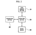
- data management device of a large-block flash memory includes a user request section 21 for requesting a data operation of the flash memory using a predetermined logical address, a converting section 22 for converting the logical address, which is used when the data operation is requested, into a physical address by means of a mapping table, and an operating section 23 for performing a predetermined data operation in the flash memory through a device driver 24, which controls the operation of the flash memory according to the converted physical address.
- the user may request the data operation by means of a predetermined user program included in the user request section 21.
- the logical address is converted into a physical address of the flash memory by a predetermined mapping table in the converting section 22 (operation S2).
- the operating section 23 controls the device driver 24, which controls the operation of the flash memory, by the converted physical address, so that the data operation requested by the user is performed (operation S3).
- operation S4 it is judged whether or not a data operation of all logical addresses used by the user has been completed. As a result of the judgment, if the data operation of all logical addresses used by the user has not been completed, the next logical address is converted into a corresponding physical address (operation S5), operation S3 of performing the data operation is again performed with respect to the converted physical address.
- the operating section 23 accesses each page including each physical address according to the sequence of the physical addresses and performs the data operation.
- the operating section 23 repeatedly accesses the same page to perform a data operation.
- the operating section 23 performs the data operation first with respect to a physical address corresponding to logical address '0', and then with respect to the respective physical addresses of logical address '1', logical address '2', logical address '3', logical address '4', and logical address '5', in regular sequence.
- the operating section 23 accesses the respective pages including each physical address corresponding to each logical address in regular sequence, and performs the data operation with respect to the physical addresses corresponding to each logical address.
- the operating section 23 performs the data operation with respect to only one physical address in a corresponding sequence.
- the data management device of the flash memory repeatedly accesses the same page to perform the data operation of the respective physical addresses.
- the present invention provides a data management device and a data management method for a flash memory which can perform an optimal data operation, by performing the data operation with respect to physical addresses included in the same page through only one page access.
- a data management device for a flash memory, the data management device comprising: a converting section for converting logical addresses into physical addresses; a rearrangement section for classifying and rearranging the physical addresses for each of physical data operation units; and an operating section for extracting the rearranged physical addresses in a physical data operation unit and performing a predetermined data operation with respect to the extracted physical addresses.
- the rearrangement section may create an address list in which address information including the converted physical addresses and corresponding logical addresses are arranged according to the sequence of the physical addresses.
- the rearrangement section may classify the address information included in the address list according to pages.
- the operating section may erase address information extracted for the data operation from the address list.
- a method of managing data in a flash memory comprising: a) converting logical addresses into physical addresses; b) rearranging the converted physical addresses according to the sequence of the physical addresses; and c) classifying the rearranged physical addresses in a physical data operation unit.
- Step b) may comprise creating address information including the converted physical addresses and corresponding logical addresses; and creating an address list in which the created address information is arranged according to the sequence of the converted physical addresses.
- the method may further comprise: d) extracting address information in a physical data operation unit; and e) performing a data operation with respect to physical addresses corresponding to the extracted address information.
- Step e) may further comprise erasing address information used through the data operation from the address list.
- flash memories are classified into small-block flash memories and large-block flash memories.
- the small-block flash memory has a characteristic that the size of a page, which is an actually physical data operation unit, is identical to that of a sector, which is a logical data operation unit.
- the large-block flash memory has a characteristic that the size of a page, which is an actually physical data operation unit, is larger than that of a sector, which is a logical data operation unit.
- the sector is a logical data operation unit used when a user performs data operations, such as a data reading operation, a data writing operation, etc., in the flash memory by means of a predetermined user program.
- the page which is a physical data operation unit used when a data operation is actually performed in the flash memory, includes an operation unit for reading data from the flash memory and an operation unit for writing data into the flash memory.
- the physical data operation unit is not limited to the page, but may be defined in various sizes, for example, a block, according to used devices.
- the large-block flash memory includes a block 100, wherein the block 100 includes a plurality of pages 120, and each page 120 includes a plurality of sectors 110.
- each page 120 has a size of 2 Kbytes when the sector has a size of 512 bytes.
- the sector 110 is a logical data operation unit
- the page 120 is a physical data operation unit.
- the user requests a predetermined data operation to the flash memory using logical addresses, and the logical addresses may be mapped on predetermined sectors in the flash memory.
- the respective logical addresses may be mapped so as to correspond to the physical addresses using a predetermined mapping table as shown in Figure 6.
- the data operation is performed with respect to a physical address corresponding to the logical address according to the mapping table in the flash memory.
- the data operation is performed with respect to physical addresses corresponding to logical addresses requested by the user. In this case, even when multiple physical addresses are included in the same page, the data operation is performed in the sequence of the logical addresses, so that separate data operation must be performed with respect to each of the logical addresses, and thus it becomes impossible to perform an optimal data operation.
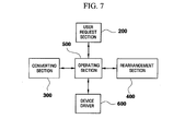
- Figure 7 is a block diagram showing a data management device of a flash memory according to an exemplary embodiment of the present invention.
- the data management device includes a user request section 200, a converting section 300, a rearrangement section 400, an operating section 500, and a device driver 600.
- the user request section 200 is used when a user requests a data operation using predetermined logical addresses.
- the converting section 300 converts the requested logical addresses into physical addresses by means of the mapping table.
- the rearrangement section 400 checks pages including the converted physical addresses, and rearranges the sequence of the physical addresses according to the sequence of the pages.
- the operating section 500 extracts physical addresses from each of the corresponding pages including the rearranged physical addresses and then performs a predetermined data operation for the extracted physical addresses.
- the device driver 600 controls the operation of the flash memory, and performs an actual data operation with respect to relevant physical addresses according to the control the operating section 500.
- the user request section 200 includes a user program which enable a user to request a predetermined data operation using the logical addresses.
- the converting section 300 includes a mapping table needed when logical addresses used by the user are converted into corresponding physical addresses.
- Physical addresses converted by the converting section 300 are transferred with corresponding logical addresses to the rearrangement section 400.
- the rearrangement section 400 creates address information which includes the converted physical addresses and the corresponding logical addresses, and creates an address list by arranging the address information according to the sequence of the physical addresses.
- the operating section 500 extracts address information according to pages from the address list rearranged by the rearrangement section 400, and reads the extracted address information according to pages to perform a data operation for relevant physical addresses.
- address information corresponding to physical addresses having undergone the data operation may be erased from the address list.
- a data management method of the flash memory having the above-mentioned construction according to the present invention is as follows.
- a user requests a data operation of the flash memory using predetermined logical addresses (operation S110).
- the requested logical address is identical to the physical address actually used for a data operation because a logical data operation unit is identical to a physical data operation unit.
- a logical data operation unit is smaller than a physical data operation unit, so that a process of converting the requested logical addresses into physical addresses is required.
- the present embodiment will be explained with respect to the case in which the flash memory is a large-block flash memory.
- the logical addresses are converted into physical addresses, which are actually used for a data operation in the flash memory, by means of the mapping table (operation S120).
- the converted physical addresses and corresponding logical addresses are transferred to the rearrangement section 400, and the rearrangement section 400 creates address information including the converted physical addresses and the corresponding logical addresses (operation S130).
- the address information includes logical address used by the user and physical addresses corresponding to the logical addresses in the mapping table.
- the rearrangement section 400 rearranges the created address information according to the sequence of the converted physical addresses, thereby creating an address list (operation S140).
- the address list contains address information 700 which includes physical addresses 710, which have been converted by the converting section 300, and corresponding logical addresses 720, and are arranged according to the sequence of the physical addresses 710.
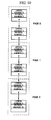
- the rearrangement section 400 classifies the address information, which is included in the address list, according to pages, each of which is a physical data operation unit (operation S150).
- the address information included in the address list created by the rearrangement section 400 is classified by the page according to physical addresses included in the address information.
- the operating section 500 extracts address information included in a first page, that is, page '0', from among the address information included in the address list (operation S160), and performs the data operation requested by the user with respect to physical addresses of the extracted address information (operation S170).
- the address information having undergone the data operation is erased from the address list (operation S180), and it is judged whether or not all address information included in the address list has been extracted (operation S190).
- address information included in the next page is extracted (operation S200) to repeat steps 170 and 180 of performing the data operation with respect to the extracted address information.
- address information extracted for the data operation may be erased from the address list after the data operation is performed.
- the logical addresses are converted into physical addresses by the mapping table in the converting section 300 (operation S320).
- the converted physical addresses and corresponding logical addresses are transferred to the rearrangement section 400, and the rearrangement section 400 creates address information including the converted physical addresses and the corresponding logical addresses (operation S330).
- the rearrangement section 400 rearranges the created address information according to the sequence of the physical addresses, thereby creating an address list (operation S340).
- the operating section 500 extracts address information having physical addresses included in a first page from among the address list (operation S350).
- the operating section 500 reads data recorded in the physical addresses which are included in the extracted address information (operation S360).
- the address information, from which the data have been read, is erased from the address list (operation S370), and then it is judged whether or not all address information included in the address list has been extracted (operation S380).
- logical addresses used by a user are logical address '0' to logical address '5', logical address '0' to logical address '5' are all included in three pages according to the mapping table.
- the operating section 500 extracts address information having physical addresses according to pages from the address list, thereby reading data recorded in relevant physical addresses through only three repetitions of page accesses.
- the logical addresses used for the data writing operation are converted into physical addresses for the flash memory by the mapping table in the converting section 300 (operation S420).
- the converted physical addresses and corresponding logical addresses are transferred to the rearrangement section 400, and the rearrangement section 400 creates address information including the converted physical addresses and the corresponding logical addresses (operation 5430).
- the rearrangement section 400 rearranges the created address information according to the sequence of the physical addresses included in the address information, thereby creating an address list (operation 5440).
- the operating section 500 classifies the address information included in the created address according to pages, and extracts address information included in a first page (operation 5450).
- Predetermined data are recorded in physical addresses of the extracted address information (operation 5460).
- the address information having the physical addresses on which recording of the data has been completed is erased from the address list (operation S470).
- operations 5460 and S470 of writing predetermined data into physical addresses of the extracted address information are repeatedly performed, together with the operation of extracting address information according to pages, until all address information included in the address list are extracted.
- logical addresses used by a user are logical address '0' to logical address '5', logical address '0' to logical address '5' are all included in three pages according to the mapping table.
- the operating section 500 extracts address information having physical addresses according to pages from the address list, so that it is possible to write predetermined data into relevant physical addresses through only three repetitions of page accesses.
- the data management device and method according to present invention can reduce time required for the data operation in a large-block flash memory, in which a physical data operation unit is larger than a logical data operation unit. As a result, the data management device and method according to present invention enable an optimal data operation.
Abstract
Description
- The present invention relates to a data management device and a data management method for a large-block flash memory.
- An aim of the present invention is to improve inefficient data operation of the flash memory, which may be caused because a logical data operation unit is smaller than a physical data operation unit in a large-block flash memory.
- In general, flash memories may be used as storage media for storing and processing data in embedded systems, such as electric home appliances, communication devices, set-top boxes, etc.
- The flash memory is a nonvolatile storage device which data can be electrically erased from and rewritten into. As compared with storage media based on magnetic disk memories, the storage medium based on such a flash memory has an access time as fast as that of a hard disk while causing a smaller power consumption, and is suitable for portable devices owing to its small size.
- In the flash memory, when new data are overwritten on pre-written data, a process of erasing the whole block, in which the pre-written data are stored, is required due to a hardware characteristic of the flash memory.
- In order to prevent the performance deterioration of the flash memory, which may occur due to discordance between a data writing unit and a data erasure unit in the flash memory, concepts of a logical address and a physical address are introduced.
- Herein, the logical address is an address used when a user requests a data operation, such as data reading, data writing, etc., in the flash memory through a predetermined user program, and the physical address is an address used when the flash memory actually performs the data operation, such as data reading, data writing, etc.
- Flash memories are generally classified into small-block flash memories and large-block flash memories. The small-block flash memory has a characteristic that the size of an actually physical data operation unit is identical to that of a logical data operation unit, but the large-block flash memory has a characteristic that the size of an actually physical data operation unit is larger than that of a logical data operation unit.
- As shown in Figure 1, a general large-block flash memory includes a
sector 11 which is a logical data operation unit, apage 12 which is a physical data operation unit, and ablock 13 which is a data erasure unit. - One page in the large-block flash memory includes a plurality of sectors, while one page in the small-block flash memory includes only one sector.
- As shown in Figure 2, data management device of a large-block flash memory includes a
user request section 21 for requesting a data operation of the flash memory using a predetermined logical address, a convertingsection 22 for converting the logical address, which is used when the data operation is requested, into a physical address by means of a mapping table, and anoperating section 23 for performing a predetermined data operation in the flash memory through adevice driver 24, which controls the operation of the flash memory according to the converted physical address. - In the following description, the operation of the data management device of the large-block flash memory having the above-mentioned construction will be explained with reference to Figure 3. First, a user requests a data operation of the flash memory using a predetermined logical address (operation S1).
- In this case, the user may request the data operation by means of a predetermined user program included in the
user request section 21. - The logical address is converted into a physical address of the flash memory by a predetermined mapping table in the converting section 22 (operation S2).
- The
operating section 23 controls thedevice driver 24, which controls the operation of the flash memory, by the converted physical address, so that the data operation requested by the user is performed (operation S3). - Then, it is judged whether or not a data operation of all logical addresses used by the user has been completed (operation S4). As a result of the judgment, if the data operation of all logical addresses used by the user has not been completed, the next logical address is converted into a corresponding physical address (operation S5), operation S3 of performing the data operation is again performed with respect to the converted physical address.
- That is, in the case of the large-block flash memory, when sectors, which are physical addresses corresponding to logical addresses used when the user requests a data operation, are included in different pages from each other, the
operating section 23 accesses each page including each physical address according to the sequence of the physical addresses and performs the data operation. - Therefore, even when multiple physical addresses are included in the same page, if they are not sequential addresses, the
operating section 23 repeatedly accesses the same page to perform a data operation. - In the following description, a data reading operation performed by the
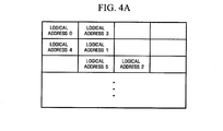
operating section 23 will be explained as an example of data operations. - First, if logical addresses used by the user are logical address '0' to logical address '5' and physical addresses corresponding to the logical addresses are positioned as shown in Figure 4A, the
operating section 23 performs the data operation first with respect to a physical address corresponding to logical address '0', and then with respect to the respective physical addresses of logical address '1', logical address '2', logical address '3', logical address '4', and logical address '5', in regular sequence. - That is, as shown in Figure 4B, the
operating section 23 accesses the respective pages including each physical address corresponding to each logical address in regular sequence, and performs the data operation with respect to the physical addresses corresponding to each logical address. - Here, even when multiple physical addresses exist in one page, if they are not sequential addresses, the
operating section 23 performs the data operation with respect to only one physical address in a corresponding sequence. - Therefore, in order to perform data operation with respect to all of logical address '0' to logical address '5', it is necessary to perform page access six times in total.
- That is, even when multiple physical addresses are included in the same page, if they are not sequential addresses, the data management device of the flash memory, as described above, repeatedly accesses the same page to perform the data operation of the respective physical addresses.
- Therefore, the time required for a data operation increases due to repeated accesses to the same page, which deteriorates the performance of the flash memory.
- According to the present invention there is provided an apparatus and method as set forth in the appended claims. Preferred features of the invention will be apparent from the dependent claims, and the description which follows.
- In one aspect, the present invention provides a data management device and a data management method for a flash memory which can perform an optimal data operation, by performing the data operation with respect to physical addresses included in the same page through only one page access.
- According to an exemplary embodiment of the present invention, there is provided a data management device for a flash memory, the data management device comprising: a converting section for converting logical addresses into physical addresses; a rearrangement section for classifying and rearranging the physical addresses for each of physical data operation units; and an operating section for extracting the rearranged physical addresses in a physical data operation unit and performing a predetermined data operation with respect to the extracted physical addresses.
- The rearrangement section may create an address list in which address information including the converted physical addresses and corresponding logical addresses are arranged according to the sequence of the physical addresses.
- The rearrangement section may classify the address information included in the address list according to pages.
- The operating section may erase address information extracted for the data operation from the address list.
- In accordance with another exemplary embodiment of the present invention, there is provided a method of managing data in a flash memory, the method comprising: a) converting logical addresses into physical addresses; b) rearranging the converted physical addresses according to the sequence of the physical addresses; and c) classifying the rearranged physical addresses in a physical data operation unit.
- Step b) may comprise creating address information including the converted physical addresses and corresponding logical addresses; and creating an address list in which the created address information is arranged according to the sequence of the converted physical addresses.
- The method may further comprise: d) extracting address information in a physical data operation unit; and e) performing a data operation with respect to physical addresses corresponding to the extracted address information.
- Step e) may further comprise erasing address information used through the data operation from the address list.
- The above and other objects, features and advantages of the present invention will be more apparent from the following detailed description taken in conjunction with the accompanying drawings, in which:
- Figure 1 is a view showing a structure of a general large-block flash memory;
- Figure 2 is a block diagram showing a conventional data management device for a flash memory;
- Figure 3 is a flowchart for explaining a conventional data management method for a flash memory;
- Figure 4A is a view showing logical addresses and physical addresses converted by a mapping table;
- Figure 4B is a view for showing a conventional data reading operation of a flash memory;
- Figure 5 is a view showing a structure of a flash memory utilized according to an exemplary embodiment in the present invention;
- Figure 6 is a view showing a mapping table employed in an exemplary embodiment of the present invention;
- Figure 7 is a block diagram showing a data management device of a flash memory according to an exemplary embodiment of the present invention;
- Figure 8 is a flowchart for explaining a data management method of a flash memory according to an exemplary embodiment of the present invention;
- Figure 9 is a view showing an example of an address list according to an exemplary embodiment of the present invention;
- Figure 10 is a view showing an example in which address information included in an address list is classified according to pages according an exemplary embodiment of to the present invention;
- Figure 11 is a flowchart for explaining a data reading operation method of a flash memory according to an exemplary embodiment of the present invention;
- Figure 12 is a view for explaining a page reading process in a data reading operation of a flash memory according to an exemplary embodiment of present invention;
- Figure 13 is a flowchart for explaining a data writing operation method of a flash memory according to an exemplary embodiment of the present invention; and
- Figure 14 is a view for explaining a page writing process in a data writing operation of a flash memory according to an exemplary embodiment of present invention.
-
- Hereinafter, exemplary embodiments of the present invention will be described in detail with reference to the accompanying drawings. Advantages and features of the present invention, and methods for achieving them will be apparent to those skilled in the art from the detailed description of the exemplary embodiments together with the accompanying drawings. However, the scope of the present invention is not limited to the exemplary embodiments disclosed in the specification, and the present invention can be realized in various types. The described exemplary embodiments are presented for helping those skilled in the art to understand the scope of the present invention, and the present invention is defined only by the scope of the claims. Additionally, the same reference numerals are used to designate the same elements throughout the specification and drawings.
- In general, flash memories are classified into small-block flash memories and large-block flash memories.
- The small-block flash memory has a characteristic that the size of a page, which is an actually physical data operation unit, is identical to that of a sector, which is a logical data operation unit. In contrast, the large-block flash memory has a characteristic that the size of a page, which is an actually physical data operation unit, is larger than that of a sector, which is a logical data operation unit.
- Herein, the sector is a logical data operation unit used when a user performs data operations, such as a data reading operation, a data writing operation, etc., in the flash memory by means of a predetermined user program.
- The page, which is a physical data operation unit used when a data operation is actually performed in the flash memory, includes an operation unit for reading data from the flash memory and an operation unit for writing data into the flash memory.
- The physical data operation unit is not limited to the page, but may be defined in various sizes, for example, a block, according to used devices.
- As shown in Figure 5, the large-block flash memory includes a
block 100, wherein theblock 100 includes a plurality ofpages 120, and eachpage 120 includes a plurality ofsectors 110. - In the exemplary embodiment, it is assumed that the
page 120 has a size four times larger than that ofsector 110, that is, eachpage 120 has a size of 2 Kbytes when the sector has a size of 512 bytes. - Herein, the
sector 110 is a logical data operation unit, and thepage 120 is a physical data operation unit. - The user requests a predetermined data operation to the flash memory using logical addresses, and the logical addresses may be mapped on predetermined sectors in the flash memory.
- That is, when physical addresses are established, as shown in Figure 5, with respect to predetermined sectors, the respective logical addresses may be mapped so as to correspond to the physical addresses using a predetermined mapping table as shown in Figure 6.
- Therefore, when a user requests a data operation using a predetermined logical address, the data operation is performed with respect to a physical address corresponding to the logical address according to the mapping table in the flash memory.
- The data operation is performed with respect to physical addresses corresponding to logical addresses requested by the user. In this case, even when multiple physical addresses are included in the same page, the data operation is performed in the sequence of the logical addresses, so that separate data operation must be performed with respect to each of the logical addresses, and thus it becomes impossible to perform an optimal data operation.
- Figure 7 is a block diagram showing a data management device of a flash memory according to an exemplary embodiment of the present invention.
- As shown in Figure 7, the data management device includes a
user request section 200, a convertingsection 300, arearrangement section 400, anoperating section 500, and adevice driver 600. Theuser request section 200 is used when a user requests a data operation using predetermined logical addresses. The convertingsection 300 converts the requested logical addresses into physical addresses by means of the mapping table. Therearrangement section 400 checks pages including the converted physical addresses, and rearranges the sequence of the physical addresses according to the sequence of the pages. Theoperating section 500 extracts physical addresses from each of the corresponding pages including the rearranged physical addresses and then performs a predetermined data operation for the extracted physical addresses. Thedevice driver 600 controls the operation of the flash memory, and performs an actual data operation with respect to relevant physical addresses according to the control theoperating section 500. - Herein, the
user request section 200 includes a user program which enable a user to request a predetermined data operation using the logical addresses. - The converting
section 300 includes a mapping table needed when logical addresses used by the user are converted into corresponding physical addresses. - Physical addresses converted by the converting
section 300 are transferred with corresponding logical addresses to therearrangement section 400. Therearrangement section 400 creates address information which includes the converted physical addresses and the corresponding logical addresses, and creates an address list by arranging the address information according to the sequence of the physical addresses. - After this, the
operating section 500 extracts address information according to pages from the address list rearranged by therearrangement section 400, and reads the extracted address information according to pages to perform a data operation for relevant physical addresses. - At this time, address information corresponding to physical addresses having undergone the data operation may be erased from the address list.
- A data management method of the flash memory having the above-mentioned construction according to the present invention is as follows.
- According to the data management method of the flash memory in accordance with an exemplary embodiment of the present invention, as shown in Figure 8, first, a user requests a data operation of the flash memory using predetermined logical addresses (operation S110).
- Herein, when the flash memory is a small-block flash memory, the requested logical address is identical to the physical address actually used for a data operation because a logical data operation unit is identical to a physical data operation unit.
- However, when the flash memory is a large-block flash memory, a logical data operation unit is smaller than a physical data operation unit, so that a process of converting the requested logical addresses into physical addresses is required.
- The present embodiment will be explained with respect to the case in which the flash memory is a large-block flash memory.
- When the requested logical addresses have been transferred to the converting
section 300, the logical addresses are converted into physical addresses, which are actually used for a data operation in the flash memory, by means of the mapping table (operation S120). - The converted physical addresses and corresponding logical addresses are transferred to the
rearrangement section 400, and therearrangement section 400 creates address information including the converted physical addresses and the corresponding logical addresses (operation S130). - Herein, the address information includes logical address used by the user and physical addresses corresponding to the logical addresses in the mapping table.
- The
rearrangement section 400 rearranges the created address information according to the sequence of the converted physical addresses, thereby creating an address list (operation S140). - As shown in Figure 9, the address list contains
address information 700 which includesphysical addresses 710, which have been converted by the convertingsection 300, and correspondinglogical addresses 720, and are arranged according to the sequence of the physical addresses 710. - After having rearranging the address list, the
rearrangement section 400 classifies the address information, which is included in the address list, according to pages, each of which is a physical data operation unit (operation S150). - That is, as shown in Figure 10, the address information included in the address list created by the
rearrangement section 400 is classified by the page according to physical addresses included in the address information. - After this, the
operating section 500 extracts address information included in a first page, that is, page '0', from among the address information included in the address list (operation S160), and performs the data operation requested by the user with respect to physical addresses of the extracted address information (operation S170). - The address information having undergone the data operation is erased from the address list (operation S180), and it is judged whether or not all address information included in the address list has been extracted (operation S190).
- As a result of the judgment, if all address information included in the address list has not been extracted, address information included in the next page is extracted (operation S200) to repeat
steps - At this time, address information extracted for the data operation may be erased from the address list after the data operation is performed.
- Hereinafter, the above-mentioned data management method of the flash memory will be described with respect to a data reading operation and a data writing operation as preferred examples of data operations.
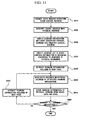
- First, in the case of the data reading operation, as shown in Figure 11, a user requests a data reading operation using logical addresses (operation S310).
- The logical addresses are converted into physical addresses by the mapping table in the converting section 300 (operation S320).
- The converted physical addresses and corresponding logical addresses are transferred to the
rearrangement section 400, and therearrangement section 400 creates address information including the converted physical addresses and the corresponding logical addresses (operation S330). - Also, the
rearrangement section 400 rearranges the created address information according to the sequence of the physical addresses, thereby creating an address list (operation S340). - The
operating section 500 extracts address information having physical addresses included in a first page from among the address list (operation S350). - After this, the
operating section 500 reads data recorded in the physical addresses which are included in the extracted address information (operation S360). - The address information, from which the data have been read, is erased from the address list (operation S370), and then it is judged whether or not all address information included in the address list has been extracted (operation S380).
- As a result of the judgment, if there is any address information which is not extracted from the address list, it is regarded that address information included in the next page exists, and the address information included in the next page is extracted (operation S390).
- After this, operations 5360 and 5370 of reading data recorded in physical addresses of the extracted address information are repeatedly performed, together with the operation of extracting address information according to pages, until all address information included in the address list are extracted.
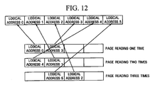
- The data reading operation described above will be described in detail with reference with Figure 12.
- When logical addresses used by a user are logical address '0' to logical address '5', logical address '0' to logical address '5' are all included in three pages according to the mapping table.
- Therefore, the
operating section 500 extracts address information having physical addresses according to pages from the address list, thereby reading data recorded in relevant physical addresses through only three repetitions of page accesses. - On the other hand, in the case of the data writing operation, as shown in Figure 13, a user requests a data writing operation, using logical addresses for performing the data writing operation (operation S410).
- The logical addresses used for the data writing operation are converted into physical addresses for the flash memory by the mapping table in the converting section 300 (operation S420).
- The converted physical addresses and corresponding logical addresses are transferred to the
rearrangement section 400, and therearrangement section 400 creates address information including the converted physical addresses and the corresponding logical addresses (operation 5430). - The
rearrangement section 400 rearranges the created address information according to the sequence of the physical addresses included in the address information, thereby creating an address list (operation 5440). - The
operating section 500 classifies the address information included in the created address according to pages, and extracts address information included in a first page (operation 5450). - Predetermined data are recorded in physical addresses of the extracted address information (operation 5460).
- The address information having the physical addresses on which recording of the data has been completed is erased from the address list (operation S470).
- After this, it is judged whether or not all address information included in the address list has been extracted (operation 5480). As a result of the judgment, if there is any address information which is not extracted from the address list, it is regarded that address information included in the next page exists, and the address information included in the next page is extracted (operation S490).
- Then, operations 5460 and S470 of writing predetermined data into physical addresses of the extracted address information are repeatedly performed, together with the operation of extracting address information according to pages, until all address information included in the address list are extracted.
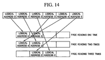
- The data writing operation described above will be described in detail with reference with Figure 14.
- When logical addresses used by a user are logical address '0' to logical address '5', logical address '0' to logical address '5' are all included in three pages according to the mapping table.
- Therefore, the
operating section 500 extracts address information having physical addresses according to pages from the address list, so that it is possible to write predetermined data into relevant physical addresses through only three repetitions of page accesses. - According to the present invention, physical addresses are classified according to pages each of which is a physical data operation unit, and a predetermined data operation is performed with respect to the classified physical addresses. Therefore, the data management device and method according to present invention can reduce time required for the data operation in a large-block flash memory, in which a physical data operation unit is larger than a logical data operation unit. As a result, the data management device and method according to present invention enable an optimal data operation.
- Although a few preferred embodiments have been shown and described, it will be appreciated by those skilled in the art that various changes and modifications might be made without departing from the scope of the invention, as defined in the appended claims.
- Attention is directed to all papers and documents which are filed concurrently with or previous to this specification in connection with this application and which are open to public inspection with this specification, and the contents of all such papers and documents are incorporated herein by reference.
- All of the features disclosed in this specification (including any accompanying claims, abstract and drawings), and/or all of the steps of any method or process so disclosed, may be combined in any combination, except combinations where at least some of such features and/or steps are mutually exclusive.
- Each feature disclosed in this specification (including any accompanying claims, abstract and drawings) may be replaced by alternative features serving the same, equivalent or similar purpose, unless expressly stated otherwise. Thus, unless expressly stated otherwise, each feature disclosed is one example only of a generic series of equivalent or similar features.
- The invention is not restricted to the details of the foregoing embodiment(s). The invention extends to any novel one, or any novel combination, of the features disclosed in this specification (including any accompanying claims, abstract and drawings), or to any novel one, or any novel combination, of the steps of any method or process so disclosed.
Claims (8)
- A data management device for a flash memory which comprises a plurality of physical data operation units (120), wherein each of the physical data operation units (120) includes at least one logical operation unit (110), the data management device comprising:a converting section (300) which converts logical addresses of a plurality of logical operation units (110) into physical addresses of the logical operation units (110);a rearrangement section (400) which rearranges the physical addresses and classifies the physical addresses according to the physical data operation units (120); andan operating section (500) which extracts physical addresses, which have been rearranged and classified by the rearrangement section (400), included in one of the physical data operation units (120), and performs a predetermined data operation with respect to the physical addresses which have been extracted.
- The data management device as claimed in claim 1, wherein the rearrangement section (400) rearranges the physical address by creating an address list in which address information including the physical addresses and corresponding logical addresses are arranged according to a sequence of the physical addresses.
- The data management device as claimed in claim 2, wherein each of the physical data operation units (120) comprises a page, and the rearrangement section (400) classifies the physical addresses by grouping the address information included the address list according to pages.
- The data management device as claimed in claim 3, wherein the operating section (500) erases from the address list address information which has been extracted for performing the predetermined data operation.
- A method of managing data in a flash memory which comprises a plurality of physical data operation units (120), wherein each of the physical data operation units (120) includes at least one logical operation unit (110), the method comprising:a) converting logical addresses of a plurality of logical operation units (110) into physical addresses of the logical operation units (110);b) rearranging the physical addresses according to a sequence of the physical addresses; andc) classifying the physical addresses, which have been rearranged, according to the physical data operation units (120).
- The method as claimed in claim 5, wherein step b) comprises:creating address information including the physical addresses and corresponding logical addresses; andcreating an address list in which the created address information is arranged according to a sequence of the physical addresses, andwherein step c) comprises classifying the address information included the address list according to the physical data operation units (120).
- The method as claimed in claim 6, further comprising:d) extracting address information included in one of the physical data operation units (120); ande) performing a data operation with respect to physical addresses corresponding to the address information which has been extracted.
- The method as claimed in claim 7, wherein step e) further comprises erasing from the address list address information used for performing the data operation.
Applications Claiming Priority (2)
| Application Number | Priority Date | Filing Date | Title |
|---|---|---|---|
| KR10-2003-0097486A KR100533682B1 (en) | 2003-12-26 | 2003-12-26 | Data managing device and method for flash memory |
| KR2003097486 | 2003-12-26 |
Publications (2)
| Publication Number | Publication Date |
|---|---|
| EP1548600A1 true EP1548600A1 (en) | 2005-06-29 |
| EP1548600B1 EP1548600B1 (en) | 2007-01-24 |
Family
ID=34545912
Family Applications (1)
| Application Number | Title | Priority Date | Filing Date |
|---|---|---|---|
| EP04257934A Active EP1548600B1 (en) | 2003-12-26 | 2004-12-17 | Data management device and method for flash memory |
Country Status (6)
| Country | Link |
|---|---|
| US (1) | US7526600B2 (en) |
| EP (1) | EP1548600B1 (en) |
| JP (1) | JP2005196769A (en) |
| KR (1) | KR100533682B1 (en) |
| CN (1) | CN1321378C (en) |
| DE (1) | DE602004004494T2 (en) |
Cited By (2)
| Publication number | Priority date | Publication date | Assignee | Title |
|---|---|---|---|---|
| WO2008150927A2 (en) * | 2007-05-30 | 2008-12-11 | Schooner Information Technology | System including a fine-grained memory and a less-fine-grained memory |
| US7975109B2 (en) | 2007-05-30 | 2011-07-05 | Schooner Information Technology, Inc. | System including a fine-grained memory and a less-fine-grained memory |
Families Citing this family (23)
| Publication number | Priority date | Publication date | Assignee | Title |
|---|---|---|---|---|
| KR100659475B1 (en) * | 2005-05-26 | 2006-12-20 | 영남대학교 산학협력단 | The Reordering Buffer Architecture for Layer of Zigbee |
| US8566479B2 (en) * | 2005-10-20 | 2013-10-22 | International Business Machines Corporation | Method and system to allow logical partitions to access resources |
| JP4984666B2 (en) * | 2006-06-12 | 2012-07-25 | ソニー株式会社 | Non-volatile memory |
| JP4498341B2 (en) * | 2006-11-20 | 2010-07-07 | 株式会社東芝 | Memory system |
| US8732386B2 (en) | 2008-03-20 | 2014-05-20 | Sandisk Enterprise IP LLC. | Sharing data fabric for coherent-distributed caching of multi-node shared-distributed flash memory |
| US8229945B2 (en) | 2008-03-20 | 2012-07-24 | Schooner Information Technology, Inc. | Scalable database management software on a cluster of nodes using a shared-distributed flash memory |
| US20090265521A1 (en) * | 2008-04-18 | 2009-10-22 | Mediatek Inc. | Pattern protection method and circuit |
| JP5066209B2 (en) * | 2010-03-18 | 2012-11-07 | 株式会社東芝 | Controller, data storage device, and program |
| US9047351B2 (en) | 2010-04-12 | 2015-06-02 | Sandisk Enterprise Ip Llc | Cluster of processing nodes with distributed global flash memory using commodity server technology |
| US8856593B2 (en) | 2010-04-12 | 2014-10-07 | Sandisk Enterprise Ip Llc | Failure recovery using consensus replication in a distributed flash memory system |
| US8868487B2 (en) | 2010-04-12 | 2014-10-21 | Sandisk Enterprise Ip Llc | Event processing in a flash memory-based object store |
| US9164554B2 (en) | 2010-04-12 | 2015-10-20 | Sandisk Enterprise Ip Llc | Non-volatile solid-state storage system supporting high bandwidth and random access |
| US8725951B2 (en) | 2010-04-12 | 2014-05-13 | Sandisk Enterprise Ip Llc | Efficient flash memory-based object store |
| US8954385B2 (en) | 2010-06-28 | 2015-02-10 | Sandisk Enterprise Ip Llc | Efficient recovery of transactional data stores |
| CN102467460B (en) * | 2010-11-12 | 2014-02-26 | 群联电子股份有限公司 | Data management method, memory controller and memory storage device |
| US8694733B2 (en) | 2011-01-03 | 2014-04-08 | Sandisk Enterprise Ip Llc | Slave consistency in a synchronous replication environment |
| US8874515B2 (en) | 2011-04-11 | 2014-10-28 | Sandisk Enterprise Ip Llc | Low level object version tracking using non-volatile memory write generations |
| US9135064B2 (en) | 2012-03-07 | 2015-09-15 | Sandisk Enterprise Ip Llc | Fine grained adaptive throttling of background processes |
| TWI454913B (en) * | 2012-06-26 | 2014-10-01 | Phison Electronics Corp | Data writing method, memory controller and memory storage device |
| CN103049389B (en) * | 2012-12-14 | 2016-08-03 | 锐迪科科技有限公司 | Nand flash memory controller and write-in control method thereof |
| US9778848B2 (en) * | 2014-12-23 | 2017-10-03 | Intel Corporation | Method and apparatus for improving read performance of a solid state drive |
| US20210272619A1 (en) * | 2020-02-28 | 2021-09-02 | Western Digital Technologies, Inc. | Data Storage With Improved Read Performance By Avoiding Line Discharge |
| US11126369B1 (en) | 2020-02-28 | 2021-09-21 | Western Digital Technologies, Inc. | Data storage with improved suspend resume performance |
Citations (3)
| Publication number | Priority date | Publication date | Assignee | Title |
|---|---|---|---|---|
| US4183090A (en) * | 1977-04-20 | 1980-01-08 | Hitachi, Ltd. | Magnetic bubble memory equipment |
| US5630093A (en) * | 1990-12-31 | 1997-05-13 | Intel Corporation | Disk emulation for a non-volatile semiconductor memory utilizing a mapping table |
| US6112265A (en) * | 1997-04-07 | 2000-08-29 | Intel Corportion | System for issuing a command to a memory having a reorder module for priority commands and an arbiter tracking address of recently issued command |
Family Cites Families (17)
| Publication number | Priority date | Publication date | Assignee | Title |
|---|---|---|---|---|
| JPH04278651A (en) | 1991-03-07 | 1992-10-05 | Nec Corp | Main storage device |
| US6757800B1 (en) * | 1995-07-31 | 2004-06-29 | Lexar Media, Inc. | Increasing the memory performance of flash memory devices by writing sectors simultaneously to multiple flash memory devices |
| JPH0991975A (en) | 1995-09-28 | 1997-04-04 | Nec Corp | Data storing unit nonvolatile memory |
| JP3702515B2 (en) | 1995-12-04 | 2005-10-05 | 富士通株式会社 | Flash memory control method and flash memory control unit |
| US6078985A (en) * | 1997-04-23 | 2000-06-20 | Micron Technology, Inc. | Memory system having flexible addressing and method using tag and data bus communication |
| US5937425A (en) * | 1997-10-16 | 1999-08-10 | M-Systems Flash Disk Pioneers Ltd. | Flash file system optimized for page-mode flash technologies |
| KR100319598B1 (en) * | 1998-03-18 | 2002-04-06 | 김영환 | Flash memory array access method and device |
| KR19990079321A (en) | 1998-04-03 | 1999-11-05 | 김영환 | How to Read and Write Data in Flash Memory |
| US6427186B1 (en) * | 1999-03-30 | 2002-07-30 | Frank (Fong-Long) Lin | Memory, interface system and method for mapping logical block numbers to physical sector numbers in a flash memory, using a master index table and a table of physical sector numbers |
| KR20010105824A (en) | 2000-05-18 | 2001-11-29 | 서진원 | Automatic advertisement system using bulletin board of internet web-site |
| JP3472256B2 (en) | 2000-10-17 | 2003-12-02 | 株式会社東芝 | Data processing device and data processing method |
| US7020739B2 (en) * | 2000-12-06 | 2006-03-28 | Tdk Corporation | Memory controller, flash memory system having memory controller and method for controlling flash memory device |
| JP4256600B2 (en) * | 2001-06-19 | 2009-04-22 | Tdk株式会社 | MEMORY CONTROLLER, FLASH MEMORY SYSTEM PROVIDED WITH MEMORY CONTROLLER, AND FLASH MEMORY CONTROL METHOD |
| US6760805B2 (en) * | 2001-09-05 | 2004-07-06 | M-Systems Flash Disk Pioneers Ltd. | Flash management system for large page size |
| TWI240861B (en) * | 2002-01-11 | 2005-10-01 | Integrated Circuit Solution In | Data access method and architecture of flash memory |
| US6839826B2 (en) * | 2002-02-06 | 2005-01-04 | Sandisk Corporation | Memory device with pointer structure to map logical to physical addresses |
| US6895464B2 (en) * | 2002-06-03 | 2005-05-17 | Honeywell International Inc. | Flash memory management system and method utilizing multiple block list windows |
-
2003
- 2003-12-26 KR KR10-2003-0097486A patent/KR100533682B1/en active IP Right Grant
-
2004
- 2004-12-06 US US11/003,400 patent/US7526600B2/en active Active
- 2004-12-17 DE DE602004004494T patent/DE602004004494T2/en active Active
- 2004-12-17 EP EP04257934A patent/EP1548600B1/en active Active
- 2004-12-21 JP JP2004369991A patent/JP2005196769A/en active Pending
- 2004-12-23 CN CNB2004101017114A patent/CN1321378C/en active Active
Patent Citations (3)
| Publication number | Priority date | Publication date | Assignee | Title |
|---|---|---|---|---|
| US4183090A (en) * | 1977-04-20 | 1980-01-08 | Hitachi, Ltd. | Magnetic bubble memory equipment |
| US5630093A (en) * | 1990-12-31 | 1997-05-13 | Intel Corporation | Disk emulation for a non-volatile semiconductor memory utilizing a mapping table |
| US6112265A (en) * | 1997-04-07 | 2000-08-29 | Intel Corportion | System for issuing a command to a memory having a reorder module for priority commands and an arbiter tracking address of recently issued command |
Cited By (4)
| Publication number | Priority date | Publication date | Assignee | Title |
|---|---|---|---|---|
| WO2008150927A2 (en) * | 2007-05-30 | 2008-12-11 | Schooner Information Technology | System including a fine-grained memory and a less-fine-grained memory |
| WO2008150927A3 (en) * | 2007-05-30 | 2009-03-12 | Schooner Information Technolog | System including a fine-grained memory and a less-fine-grained memory |
| US7975109B2 (en) | 2007-05-30 | 2011-07-05 | Schooner Information Technology, Inc. | System including a fine-grained memory and a less-fine-grained memory |
| US8244969B2 (en) | 2007-05-30 | 2012-08-14 | Schooner Information Technology, Inc. | System including a fine-grained memory and a less-fine-grained memory |
Also Published As
| Publication number | Publication date |
|---|---|
| JP2005196769A (en) | 2005-07-21 |
| DE602004004494D1 (en) | 2007-03-15 |
| CN1637724A (en) | 2005-07-13 |
| CN1321378C (en) | 2007-06-13 |
| KR20050066228A (en) | 2005-06-30 |
| KR100533682B1 (en) | 2005-12-05 |
| US20050144421A1 (en) | 2005-06-30 |
| DE602004004494T2 (en) | 2007-10-31 |
| US7526600B2 (en) | 2009-04-28 |
| EP1548600B1 (en) | 2007-01-24 |
Similar Documents
| Publication | Publication Date | Title |
|---|---|---|
| EP1548600A1 (en) | Data management device and method for flash memory | |
| TWI421684B (en) | Reprogrammable non-volatile memory system and method of operating a non-volatile memory system | |
| US8205063B2 (en) | Dynamic mapping of logical ranges to write blocks | |
| US7882300B2 (en) | Apparatus and method for managing nonvolatile memory | |
| US20080098195A1 (en) | Memory system including flash memory and mapping table management method | |
| JP4960705B2 (en) | Adaptive deterministic grouping of blocks into multi-block units | |
| US8190811B2 (en) | Defragmentation of solid state memory | |
| JP2009503729A (en) | Interface system that operates with logical address space and direct data file method | |
| US11630766B2 (en) | Memory system and operating method thereof | |
| US20080195833A1 (en) | Systems, methods and computer program products for operating a data processing system in which a file system's unit of memory allocation is coordinated with a storage system's read/write operation unit | |
| EP2631916A1 (en) | Data deletion method and device | |
| JP4977703B2 (en) | Non-volatile memory with scheduled playback operation | |
| CN101120414A (en) | Data relocation in a memory system | |
| TW200301422A (en) | Hybrid density memory card | |
| US7519764B2 (en) | Apparatus and method for detecting data validity in flash memory | |
| JP5266250B2 (en) | Use of direct data file system with continuous logical address space interface | |
| US8127072B2 (en) | Data storage device and method for accessing flash memory | |
| US20130103893A1 (en) | System comprising storage device and related methods of operation | |
| JP5068754B2 (en) | Improved host interface | |
| JP4441577B2 (en) | Conversion data unit storage in memory system with fixed size storage block | |
| US20120191897A1 (en) | Non-volatile memory system and management method thereof | |
| US8745312B2 (en) | Storage device and method of mapping a nonvolatile memory based on a map history | |
| US20050169058A1 (en) | Data management apparatus and method used for flash memory | |
| US7657697B2 (en) | Method of controlling a semiconductor memory device applied to a memory card | |
| KR20120054502A (en) | Semiconductor memory device |
Legal Events
| Date | Code | Title | Description |
|---|---|---|---|
| PUAI | Public reference made under article 153(3) epc to a published international application that has entered the european phase |
Free format text: ORIGINAL CODE: 0009012 |
|
| 17P | Request for examination filed |
Effective date: 20050114 |
|
| AK | Designated contracting states |
Kind code of ref document: A1 Designated state(s): AT BE BG CH CY CZ DE DK EE ES FI FR GB GR HU IE IS IT LI LT LU MC NL PL PT RO SE SI SK TR |
|
| AX | Request for extension of the european patent |
Extension state: AL BA HR LV MK YU |
|
| AKX | Designation fees paid |
Designated state(s): DE FI FR GB IT NL |
|
| GRAP | Despatch of communication of intention to grant a patent |
Free format text: ORIGINAL CODE: EPIDOSNIGR1 |
|
| GRAS | Grant fee paid |
Free format text: ORIGINAL CODE: EPIDOSNIGR3 |
|
| GRAA | (expected) grant |
Free format text: ORIGINAL CODE: 0009210 |
|
| AK | Designated contracting states |
Kind code of ref document: B1 Designated state(s): DE FI FR GB IT NL |
|
| REG | Reference to a national code |
Ref country code: GB Ref legal event code: FG4D |
|
| REF | Corresponds to: |
Ref document number: 602004004494 Country of ref document: DE Date of ref document: 20070315 Kind code of ref document: P |
|
| ET | Fr: translation filed | ||
| PLBE | No opposition filed within time limit |
Free format text: ORIGINAL CODE: 0009261 |
|
| STAA | Information on the status of an ep patent application or granted ep patent |
Free format text: STATUS: NO OPPOSITION FILED WITHIN TIME LIMIT |
|
| 26N | No opposition filed |
Effective date: 20071025 |
|
| REG | Reference to a national code |
Ref country code: FR Ref legal event code: PLFP Year of fee payment: 12 |
|
| REG | Reference to a national code |
Ref country code: FR Ref legal event code: PLFP Year of fee payment: 13 |
|
| REG | Reference to a national code |
Ref country code: FR Ref legal event code: PLFP Year of fee payment: 14 |
|
| P01 | Opt-out of the competence of the unified patent court (upc) registered |
Effective date: 20230520 |
|
| PGFP | Annual fee paid to national office [announced via postgrant information from national office to epo] |
Ref country code: NL Payment date: 20231116 Year of fee payment: 20 |
|
| PGFP | Annual fee paid to national office [announced via postgrant information from national office to epo] |
Ref country code: GB Payment date: 20231026 Year of fee payment: 20 |
|
| PGFP | Annual fee paid to national office [announced via postgrant information from national office to epo] |
Ref country code: IT Payment date: 20231110 Year of fee payment: 20 Ref country code: FR Payment date: 20231024 Year of fee payment: 20 Ref country code: FI Payment date: 20231218 Year of fee payment: 20 Ref country code: DE Payment date: 20231024 Year of fee payment: 20 |