EP1496470A1 - Dual-mode chip card - Google Patents
Dual-mode chip card Download PDFInfo
- Publication number
- EP1496470A1 EP1496470A1 EP04300437A EP04300437A EP1496470A1 EP 1496470 A1 EP1496470 A1 EP 1496470A1 EP 04300437 A EP04300437 A EP 04300437A EP 04300437 A EP04300437 A EP 04300437A EP 1496470 A1 EP1496470 A1 EP 1496470A1
- Authority
- EP
- European Patent Office
- Prior art keywords
- contacts
- contact
- mode
- antenna
- smart card
- Prior art date
- Legal status (The legal status is an assumption and is not a legal conclusion. Google has not performed a legal analysis and makes no representation as to the accuracy of the status listed.)
- Granted
Links
- 230000005284 excitation Effects 0.000 claims abstract description 14
- 238000012545 processing Methods 0.000 claims abstract description 5
- 238000004891 communication Methods 0.000 claims description 10
- 230000005540 biological transmission Effects 0.000 claims description 4
- 238000001514 detection method Methods 0.000 description 3
- 101150064138 MAP1 gene Proteins 0.000 description 2
- 230000008901 benefit Effects 0.000 description 2
- 230000009977 dual effect Effects 0.000 description 2
- 230000005672 electromagnetic field Effects 0.000 description 2
- 230000006870 function Effects 0.000 description 2
- 238000011144 upstream manufacturing Methods 0.000 description 2
- 238000013459 approach Methods 0.000 description 1
- 239000003990 capacitor Substances 0.000 description 1
- 230000008878 coupling Effects 0.000 description 1
- 238000010168 coupling process Methods 0.000 description 1
- 238000005859 coupling reaction Methods 0.000 description 1
- 230000001939 inductive effect Effects 0.000 description 1
- 238000000034 method Methods 0.000 description 1
- 238000012986 modification Methods 0.000 description 1
- 230000004048 modification Effects 0.000 description 1
- 230000008569 process Effects 0.000 description 1
- 230000033764 rhythmic process Effects 0.000 description 1
- 230000007704 transition Effects 0.000 description 1
Images
Classifications
-
- G—PHYSICS
- G06—COMPUTING; CALCULATING OR COUNTING
- G06K—GRAPHICAL DATA READING; PRESENTATION OF DATA; RECORD CARRIERS; HANDLING RECORD CARRIERS
- G06K19/00—Record carriers for use with machines and with at least a part designed to carry digital markings
- G06K19/06—Record carriers for use with machines and with at least a part designed to carry digital markings characterised by the kind of the digital marking, e.g. shape, nature, code
- G06K19/067—Record carriers with conductive marks, printed circuits or semiconductor circuit elements, e.g. credit or identity cards also with resonating or responding marks without active components
- G06K19/07—Record carriers with conductive marks, printed circuits or semiconductor circuit elements, e.g. credit or identity cards also with resonating or responding marks without active components with integrated circuit chips
- G06K19/077—Constructional details, e.g. mounting of circuits in the carrier
- G06K19/07749—Constructional details, e.g. mounting of circuits in the carrier the record carrier being capable of non-contact communication, e.g. constructional details of the antenna of a non-contact smart card
- G06K19/07766—Constructional details, e.g. mounting of circuits in the carrier the record carrier being capable of non-contact communication, e.g. constructional details of the antenna of a non-contact smart card comprising at least a second communication arrangement in addition to a first non-contact communication arrangement
- G06K19/07769—Constructional details, e.g. mounting of circuits in the carrier the record carrier being capable of non-contact communication, e.g. constructional details of the antenna of a non-contact smart card comprising at least a second communication arrangement in addition to a first non-contact communication arrangement the further communication means being a galvanic interface, e.g. hybrid or mixed smart cards having a contact and a non-contact interface
-
- G—PHYSICS
- G06—COMPUTING; CALCULATING OR COUNTING
- G06K—GRAPHICAL DATA READING; PRESENTATION OF DATA; RECORD CARRIERS; HANDLING RECORD CARRIERS
- G06K19/00—Record carriers for use with machines and with at least a part designed to carry digital markings
- G06K19/06—Record carriers for use with machines and with at least a part designed to carry digital markings characterised by the kind of the digital marking, e.g. shape, nature, code
- G06K19/067—Record carriers with conductive marks, printed circuits or semiconductor circuit elements, e.g. credit or identity cards also with resonating or responding marks without active components
- G06K19/07—Record carriers with conductive marks, printed circuits or semiconductor circuit elements, e.g. credit or identity cards also with resonating or responding marks without active components with integrated circuit chips
- G06K19/0723—Record carriers with conductive marks, printed circuits or semiconductor circuit elements, e.g. credit or identity cards also with resonating or responding marks without active components with integrated circuit chips the record carrier comprising an arrangement for non-contact communication, e.g. wireless communication circuits on transponder cards, non-contact smart cards or RFIDs
-
- G—PHYSICS
- G06—COMPUTING; CALCULATING OR COUNTING
- G06K—GRAPHICAL DATA READING; PRESENTATION OF DATA; RECORD CARRIERS; HANDLING RECORD CARRIERS
- G06K7/00—Methods or arrangements for sensing record carriers, e.g. for reading patterns
- G06K7/0008—General problems related to the reading of electronic memory record carriers, independent of its reading method, e.g. power transfer
Definitions
- the present invention relates to the field of cards so-called bi-mode chips, that is to say which are likely to establish a communication with a terminal of read-write by through physical contacts as well as through inductive coupling via an antenna.
- US Pat. No. 6,168,083 discloses a card smart dual-mode, able to operate either in a mode by contacts, either in a mode without contacts.
- This document provides to select a communication session of type without contact if an AC voltage is induced in the antenna and an operating session via contacts with a read-write terminal, in the absence of a such alternating voltage and if a DC voltage is present on the physical contacts provided for this purpose.
- the map chip is provided with two interfaces, respectively mode contactless and contact mode, with a memory of the card, as well as circuits for selecting one of these interfaces. In fact, the circuits of the smart card are activated as soon as that a sufficient supply voltage level is detected by a level detection circuit, and the contactless interface is selected if another detector detects the presence of a AC voltage across the antenna.
- a disadvantage of the system provided by this document is it does not allow a failover of a contact operation to contactless operation during the same session of operation, that is to say when the selection circuit has selected one of the interfaces. We must wait for a reset the system to allow, if necessary, a switchover by a new detection phase.
- a bi-mode smart card it would be desirable, in a bi-mode smart card, to allow a switchover from a contact operation to contactless operation during the same session of communication.
- a feature is of interest particular in the case of smart cards coupled with portable devices having a battery.
- the need to reset a communication session with the chip may impose a user intervention for a switching to a non-contact mode of operation.
- a chip electronic chip card containing information the user's default is in an operation to contacts with the rest of the cell phone.
- This chip could be associated with contactless operation, for example to allow the passage of automatic turnstiles public transit using the same chip.
- a such an application is not possible with the systems known because it would force the user to cut a communication phone to reset the smart card and allow then a selection towards a mode of operation without contact.
- the present invention aims to propose a smart card dual mode that overcomes the disadvantages of known solutions. More particularly, the invention aims to propose a smart card dual mode that is likely to switch from operation to contacts to a contactless operation during the same communication session.
- the invention also aims to propose a solution which is compatible with the desired miniaturization of cards smart.
- the invention also aims to propose a solution particularly simple to implement.
- this invention provides a bi-mode smart card comprising several physical contact pads with an external reader and two pads connection to an antenna for contactless operation, and having a voltage regulator adapted to extract from a radiofrequency excitation reaching the antenna a voltage supply of the chip processing circuits, this regulator being controllable by a central circuit to be disabled in the presence of a supply voltage on contacts of the chip, so that the chip can be powered from contacts during contactless operation.
- the central control circuit exploits the results of a radio frequency presence detector on the antenna to select a contactless operating mode or a contact mode of operation.
- the circuit control unit in the absence of a radiofrequency excitation voltage and in presence of a supply voltage by contacts, deactivates the controller and initiates a communication by the contact pads, the presence detector radio frequency signal remaining activated to allow a transition to a contactless mode of operation upon arrival possible radiofrequency excitation.
- the card further comprises asynchronous transmission means directly between a demodulator of the signals received by the antenna and at least one input-output terminal with contacts.
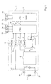
- a card 1 in a conventional manner, includes a central processing unit as well as memory (block 2, CPU + MEM) corresponding to the function classic of a smart card.
- Block 2 is connected to two pads 31 and 32 of the card 1 for receiving a supply voltage Vdd when the card is engaged in a read-write device with contacts (not shown).
- the stud 31 is for example a positive supply pad Vdd while the pad 32 is a GND ground stud.
- the smart card 1 comprises three additional contacts 33, 34 and 35 respectively to perform input / output (I / O) functions, feed a clock signal CLK from the reader and supplying a signal RST reset from the reader with contacts.
- this one also includes two pads 36 and 37 to be connected at the terminals of an antenna L in non-contact operation.
- a capacitor C connected to terminals 36 and 37 is generally integrated in card 1 and participates with the antenna L in the creation of a parallel resonant circuit capable of being excited by a electromagnetic field generated by a read-write terminal when card 1 approaches the terminal.
- the smart card 1 respects the operations planned for electromagnetic transponders according to which a carrier (for example, at 13.57 MHz) remote power is modulated to transmit data from a read-write terminal to the smart card, and that a transmission of the smart card to the terminal is performed by back-modulation at the rhythm of a subcarrier (for example, at 847 kHz).
- a bridge rectifier 4 is usually connected by its two terminals Alternative input to pads 36 and 37. Rectified output side of bridge 4, one of the terminals (for example positive) is connected at the input of a regulator 5 (RF Reg) for example linear, as well as than in the input of a demodulator 6 (Demod).
- the regulator 5 is charged to supply the rest of the board with the supply voltage necessary for its operation when this is remote powered by the electromagnetic field of a contactless terminal.
- the demodulator 6 is responsible for decoding the data transmitted by the terminal to the transponder.
- a switch K of retromodulation is generally used switching a load between the two output terminals rectified bridge 4 under control of a block 7 (Log) receiving the data to be transmitted.
- a clock signal of contactless operation to the rest of the map is extracted by a clock generation block 8 (Clock Gen) whose input is connected to one of the pads 36 and 37.
- the card 1 further comprises a circuit 9 (RF Det) for detecting the presence of an excitation radio frequency on the antenna L to detect a need for passage in contactless mode, as well as a circuit 10 (CTRL) of general order not only responsible for the selection between two modes of operation, but also the management of this operation.
- RF Det a circuit 9
- CTRL circuit 10
- the respective outputs of the regulator 5, the demodulator 6, the clock generator 8 and the radiofrequency detector 9 are sent to inputs of the control circuit 10, just as this one is connected to the pads 33, 34 and 35 of the operation with contacts.
- circuit 10 provides the data signals to the block 7 of retromodulation and exchange, with the unit circuit 2 central, data control S signals as well as power supply from terminals 31 and 32 in the contact operation. Although this is not represented, the circuit 10 exchanges signals with the different blocks of the map if it is required by their respective structures.
- a feature of the present invention is use regulator 5 only when operating without contact. As the figure shows, this one is connected in upstream of the control circuit 10 so that it does not receive a signal to regulate only when a radio frequency voltage is present in contactless operation. The rest of the time, all power is supplied by the voltage present on the terminals 31 and 32 and the regulator 5 remains disconnected. In one simplified embodiment of the regulator 5, it suffices that it does not receive signals at the output of the bridge rectifier 4, without the need for switching.
- the circuit 10 manages the different signal exchanges as follows.
- the card In the presence of radiofrequency excitation only of the smart card, that is to say while no voltage power supply does not arrive on contacts 31 and 32, the card becomes powered in the manner of an electromagnetic transponder by the regulator 5 at the same time as an excitation radio frequency is detected by the circuit 9 and that a clock is extracted from the alternative excitation by block 8.
- the map 1 then operates in contactless mode being self powered radiofrequency field and the commutations are carried out by the radiofrequency channel exclusively. In this mode of operation, the circuit 10 isolates the contacts 33, 34 and 35 during the whole session.
- the detector 9 detects the presence of a radiofrequency signal
- the block 10 who receives the information activates the demodulator 6 so to be able to exploit the signals received by the antenna.
- the regulator 5 remains deactivated, however, as long as the power supply is provided by the contacts.
- the demodulator 6 detects a data, it is transmitted by the block 10 to the CPU 2. This is then the application software who selects, according to the wishes of the application program, if one must operate then in a mode with contacts or without touching.
- the central processing unit can then process a brief interruption to validate the passage of the gate without to lose the communication, for example telephone, engaged through a contact session with the rest mobile phone.
- the radiofrequency signal detector 9 is, for for example, a detector as described in the patent application 0 903 688 of the applicant.
- An advantage of the present invention is that by providing a controllable controller upstream of the control circuit 10, it is possible to switch from a contact operation to contactless operation during the same session without risk of power conflict between the two sources possible (contacts 31 and 32, antenna terminals 36 and 37).
- a controllable circuit as is the case especially in the aforementioned US Pat. No. 6,168,083, it is not possible to switch from one mode to another during of the same session, otherwise the radio frequency power supply risk of disappearing by the external supply by studs, or Conversely.
- a smart card according to the invention may further be equipped with a transmitter asynchronous IART to transmit, without transiting to the unit unit 2, data received on the RF channel (demodulated by the block 6), to the input / output pad (s) 33 in real time.
- circuit central control unit 10 is capable of various variations and modifications that will appear to man art.
- the practical implementation of the circuit central control unit 10 is within the reach of those skilled in the art from the functional indications given above.
- the invention has been described in relation to five input / output pads for a contact operation mode, it may have a different number of contacts.
- the invention applies to all types of operation and transponder-type smart card architectures electromagnetic and all types of operation and architectures of smart cards with contacts.
Abstract
Description
La présente invention concerne le domaine des cartes à puce dites bi-mode, c'est-à-dire qui sont susceptibles d'établir une communication avec une borne de lecture-écriture par l'intermédiaire de contacts physiques ainsi que par l'intermédiaire d'un couplage inductif via une antenne.The present invention relates to the field of cards so-called bi-mode chips, that is to say which are likely to establish a communication with a terminal of read-write by through physical contacts as well as through inductive coupling via an antenna.
On connaít du brevet américain N° 6 168 083 une carte à puce bi-mode, capable de fonctionner soit dans un mode par contacts, soit dans un mode sans contacts. Ce document prévoit de sélectionner une session de communication de type sans contact si une tension alternative est induite dans l'antenne et une session de fonctionnement par l'intermédiaire des contacts physiques avec une borne de lecture-écriture, en l'absence d'une telle tension alternative et si une tension continue est présente sur les contacts physiques prévus à cet effet. La carte à puce est pourvue de deux interfaces, respectivement de mode sans contact et de mode à contacts, avec une mémoire de la carte, ainsi que de circuits de sélection d'une de ces interfaces. En fait, les circuits de la carte à puce sont activés dès qu'un niveau de tension d'alimentation suffisant est détecté par un circuit de détection de niveau, et l'interface sans contact est sélectionnée si un autre détecteur détecte la présence d'une tension alternative aux bornes de l'antenne. US Pat. No. 6,168,083 discloses a card smart dual-mode, able to operate either in a mode by contacts, either in a mode without contacts. This document provides to select a communication session of type without contact if an AC voltage is induced in the antenna and an operating session via contacts with a read-write terminal, in the absence of a such alternating voltage and if a DC voltage is present on the physical contacts provided for this purpose. The map chip is provided with two interfaces, respectively mode contactless and contact mode, with a memory of the card, as well as circuits for selecting one of these interfaces. In fact, the circuits of the smart card are activated as soon as that a sufficient supply voltage level is detected by a level detection circuit, and the contactless interface is selected if another detector detects the presence of a AC voltage across the antenna.
Un inconvénient du système prévu par ce document est qu'il n'autorise pas un basculement d'un fonctionnement à contacts vers un fonctionnement sans contact au cours d'une même session de fonctionnement, c'est-à-dire lorsque le circuit de sélection a sélectionné l'une des interfaces. Il faut alors attendre une réinitialisation du système pour, le cas échéant, autoriser un basculement par une nouvelle phase de détection.A disadvantage of the system provided by this document is it does not allow a failover of a contact operation to contactless operation during the same session of operation, that is to say when the selection circuit has selected one of the interfaces. We must wait for a reset the system to allow, if necessary, a switchover by a new detection phase.
Un autre inconvénient du système décrit par le document susmentionné est que le régulateur linéaire nécessaire pour le fonctionnement en mode sans contact introduit une dissipation d'énergie même dans le cas d'un fonctionnement avec une alimentation par contacts physiques.Another disadvantage of the system described by the document mentioned above is that the linear regulator needed for operation in contactless mode introduces dissipation of energy even in the case of operation with a power supply by physical contact.
Il serait souhaitable, dans une carte à puce bi-mode, d'autoriser un basculement d'un fonctionnement à contacts vers un fonctionnement sans contact au cours d'une même session de communication. Une telle fonctionnalité trouve un intérêt tout particulier dans le cas de cartes à puce couplées à des dispositifs portables possédant une batterie. Dans un tel cas, le besoin de réinitialiser une session de communication avec la puce peut imposer une intervention de l'utilisateur pour un basculement vers un mode de fonctionnement sans contact. Par exemple, dans une application aux téléphones portables, une puce électronique d'une carte à puce contenant des informations personnelles de l'utilisateur est par défaut dans un fonctionnement à contacts avec le reste du téléphone portable. Cette puce pourrait être associée à un fonctionnement sans contact, par exemple pour autoriser le passage de tourniquets automatiques de transport en commun au moyen de la même puce. Une telle application n'est pas envisageable avec les systèmes connus car cela obligerait l'utilisateur à couper une communication téléphonique pour réinitialiser la carte à puce et autoriser alors une sélection vers un mode de fonctionnement sans contact.It would be desirable, in a bi-mode smart card, to allow a switchover from a contact operation to contactless operation during the same session of communication. Such a feature is of interest particular in the case of smart cards coupled with portable devices having a battery. In such a case, the need to reset a communication session with the chip may impose a user intervention for a switching to a non-contact mode of operation. By example, in an application to mobile phones, a chip electronic chip card containing information the user's default is in an operation to contacts with the rest of the cell phone. This chip could be associated with contactless operation, for example to allow the passage of automatic turnstiles public transit using the same chip. A such an application is not possible with the systems known because it would force the user to cut a communication phone to reset the smart card and allow then a selection towards a mode of operation without contact.
La présente invention vise à proposer une carte à puce bi-mode qui pallie les inconvénients de solutions connues. Plus particulièrement, l'invention vise à proposer une carte à puce bi-mode qui soit susceptible de commuter d'un fonctionnement à contacts vers un fonctionnement sans contact au cours d'une même session de communication.The present invention aims to propose a smart card dual mode that overcomes the disadvantages of known solutions. More particularly, the invention aims to propose a smart card dual mode that is likely to switch from operation to contacts to a contactless operation during the same communication session.
L'invention vise également à proposer une solution qui soit compatible avec les miniaturisations recherchées des cartes à puce.The invention also aims to propose a solution which is compatible with the desired miniaturization of cards smart.
L'invention vise en outre à proposer une solution particulièrement simple à mettre en oeuvre.The invention also aims to propose a solution particularly simple to implement.
Pour atteindre ces objets et d'autres, la présente invention prévoit une carte à puce bi-mode comprenant plusieurs plots de contact physique avec un lecteur externe et deux plots de connexion à une antenne pour un fonctionnement sans contact, et comportant un régulateur de tension apte à extraire d'une excitation radiofréquence parvenant sur l'antenne une tension d'alimentation des circuits de traitement de la puce, ce régulateur étant commandable par un circuit central pour être désactivé en présence d'une tension d'alimentation sur des contacts de la puce, de sorte que la puce puisse être alimentée à partir des contacts lors d'un fonctionnement sans contact.To reach these objects and others, this invention provides a bi-mode smart card comprising several physical contact pads with an external reader and two pads connection to an antenna for contactless operation, and having a voltage regulator adapted to extract from a radiofrequency excitation reaching the antenna a voltage supply of the chip processing circuits, this regulator being controllable by a central circuit to be disabled in the presence of a supply voltage on contacts of the chip, so that the chip can be powered from contacts during contactless operation.
Selon un mode de réalisation de la présente invention, le circuit de commande central exploite les résultats d'un détecteur de présence de signaux radiofréquence sur l'antenne pour sélectionner un mode de fonctionnement sans contact ou un mode de fonctionnement à contacts.According to an embodiment of the present invention, the central control circuit exploits the results of a radio frequency presence detector on the antenna to select a contactless operating mode or a contact mode of operation.
Selon un mode de réalisation de la présente invention, en présence d'une excitation radiofréquence et en l'absence de tension d'alimentation par les contacts physiques, on entame une session de fonctionnement sans contact jusqu'à une réinitialisation complète du système.According to an embodiment of the present invention, in the presence of radiofrequency excitation and in the absence of supply voltage through physical contact, we start a non-contact operation session until a reset complete system.
Selon un mode de réalisation de la présente invention, en l'absence d'une tension d'excitation radiofréquence et en présence d'une tension d'alimentation par contacts, le circuit de commande central désactive le régulateur et initie une communication par les plots à contacts, le détecteur de présence de signaux radiofréquence restant activé pour autoriser un passage vers un mode de fonctionnement sans contact à l'arrivée d'une éventuelle excitation radiofréquence.According to an embodiment of the present invention, in the absence of a radiofrequency excitation voltage and in presence of a supply voltage by contacts, the circuit control unit deactivates the controller and initiates a communication by the contact pads, the presence detector radio frequency signal remaining activated to allow a transition to a contactless mode of operation upon arrival possible radiofrequency excitation.
Selon un mode de réalisation de la présente invention, la carte comprend en outre des moyens de transmission asynchrone directe entre un démodulateur des signaux reçus par l'antenne et au moins une borne d'entrée-sortie à contacts.According to an embodiment of the present invention, the card further comprises asynchronous transmission means directly between a demodulator of the signals received by the antenna and at least one input-output terminal with contacts.
Ces objets, caractéristiques et avantages, ainsi que d'autres de la présente invention seront exposés en détail dans la description suivante de modes de réalisation particuliers faite à titre non-limitatif en relation avec la figure jointe qui représente, de façon très schématique et sous forme de blocs, un exemple de carte à puce bi-mode selon la présente invention.These objects, features and benefits, as well as others of the present invention will be discussed in detail in the following description of particular embodiments made in a non-limiting way in relation to the attached figure which represents, very schematically and in the form of blocks, an example of a bi-mode smart card according to this invention.
Par souci de clarté, seuls les éléments nécessaires à la compréhension de l'invention ont été représentés à la figure et seront décrits par la suite. En particulier, les détails de fonctionnement des modes à contacts et sans contact n'ont pas été détaillés, l'invention s'appliquant à tous les modes de fonctionnement de cartes à puce sans contact (transpondeurs électromagnétiques) et de cartes à puce à contacts.For the sake of clarity, only the elements necessary for the understanding of the invention have been represented in the figure and will be described later. In particular, the details of operation of contact and contactless modes have not have been detailed, the invention applies to all modes of operation of contactless smart cards (transponders electromagnetic) and smart cards with contacts.
De façon classique, une carte 1 selon l'invention comprend une unité centrale de traitement ainsi que des éléments de mémorisation (bloc 2, CPU + MEM) correspondant à la fonction classique d'une carte à puce.In a conventional manner, a card 1 according to the invention includes a central processing unit as well as memory (block 2, CPU + MEM) corresponding to the function classic of a smart card.
Le bloc 2 est connecté à deux plots 31 et 32 de la
carte 1 destinés à recevoir une tension d'alimentation Vdd
lorsque la carte est engagée dans un dispositif de lecture-écriture
à contacts (non représenté). Le plot 31 est par exemple
un plot d'alimentation positive Vdd tandis que le plot 32 est un
plot de masse GND.Block 2 is connected to two
Dans l'exemple représenté, la carte à puce 1 comporte
trois contacts additionnels 33, 34 et 35 destinés respectivement
à remplir des fonctions d'entrée/sortie (I/O), d'amenée d'un
signal d'horloge CLK depuis le lecteur et d'amenée d'un signal
de réinitialisation RST depuis le lecteur à contacts.In the example shown, the smart card 1 comprises
three
S'agissant d'une carte à puce bi-mode, celle-ci
comprend également deux plots 36 et 37 destinés à être raccordés
aux bornes d'une antenne L dans un fonctionnement sans contact.
Un condensateur C connecté aux bornes 36 et 37 est généralement
intégré à la carte 1 et participe avec l'antenne L à la création
d'un circuit résonant parallèle propre à être excité par un
champ électromagnétique généré par une borne de lecture-écriture
lorsque la carte 1 s'approche de la borne. Dans ce fonctionnement,
la carte à puce 1 respecte les opérations prévues pour
les transpondeurs électromagnétiques selon lesquels une porteuse
(par exemple, à 13,57 MHz) de téléalimentation est modulée pour
transmettre des données depuis une borne de lecture-écriture
vers la carte à puce, et selon lesquels une transmission de la
carte à puce vers la borne est effectuée par rétromodulation au
rythme d'une sous porteuse (par exemple, à 847 kHz).Being a dual-mode smart card, this one
also includes two
Pour permettre une démodulation des données reçues en
mode sans contact ainsi qu'une téléalimentation de la carte, un
pont redresseur 4 est généralement connecté par ses deux bornes
d'entrée alternative aux plots 36 et 37. Côté sortie redressée
du pont 4, une des bornes (par exemple positive) est connectée
en entrée d'un régulateur 5 (RF Reg) par exemple linéaire, ainsi
qu'en entrée d'un démodulateur 6 (Demod). Le régulateur 5 est
chargé de fournir au reste de la carte la tension d'alimentation
nécessaire à son fonctionnement lorsque ceci est téléalimenté
par le champ électromagnétique d'une borne sans contact. Le
démodulateur 6 est chargé de décoder les données transmises par
la borne à destination du transpondeur.To enable demodulation of data received in
contactless mode as well as a remote power supply of the card, a
Pour une transmission de données de la carte vers le
lecteur, on utilise généralement un interrupteur K de rétromodulation
commutant une charge entre les deux bornes de sortie
redressées du pont 4 sous commande d'un bloc 7 (Log) recevant
les données à transmettre. Enfin, un signal d'horloge de
fonctionnement sans contact à destination du reste de la carte
est extrait par un bloc 8 de génération d'horloge (Clock Gen)
dont l'entrée est connectée sur l'un des plots 36 et 37.For data transmission from the card to the
reader, a switch K of retromodulation is generally used
switching a load between the two output terminals
rectified
Selon l'invention, la carte 1 comprend en plus un circuit 9 (RF Det) de détection de présence d'une excitation radiofréquence sur l'antenne L pour détecter un besoin de passage en mode sans contact, ainsi qu'un circuit 10 (CTRL) de commande générale chargé non seulement de la sélection entre les deux modes de fonctionnement, mais également de la gestion de ce fonctionnement.According to the invention, the card 1 further comprises a circuit 9 (RF Det) for detecting the presence of an excitation radio frequency on the antenna L to detect a need for passage in contactless mode, as well as a circuit 10 (CTRL) of general order not only responsible for the selection between two modes of operation, but also the management of this operation.
Selon l'invention, les sorties respectives du régulateur
5, du démodulateur 6, du générateur d'horloge 8 et du
détecteur radiofréquence 9 sont envoyés sur des entrées du
circuit de contrôle 10, de même que celui-ci est relié aux plots
33, 34 et 35 du fonctionnement à contacts. Par ailleurs, le
circuit 10 fournit les signaux de données à destination du bloc
7 de rétromodulation et échange, avec le circuit 2 d'unité
centrale, des signaux S de commande de données ainsi que
d'alimentation provenant des bornes 31 et 32 dans le mode de
fonctionnement à contacts. Bien que cela ne soit pas représenté,
le circuit 10 échange des signaux avec les différents blocs de
la carte si cela est requis par leurs structures respectives.According to the invention, the respective outputs of the
Une caractéristique de la présente invention est de
n'utiliser le régulateur 5 que lors d'un fonctionnement sans
contact. Comme l'illustre la figure, celui-ci est connecté en
amont du circuit 10 de contrôle de sorte qu'il ne reçoit un
signal à réguler que lorsqu'une tension radiofréquence est
présente en fonctionnement sans contact. Le reste du temps,
toute l'alimentation est fournie par la tension présente sur les
bornes 31 et 32 et le régulateur 5 reste déconnecté. Dans un
mode de réalisation simplifié du régulateur 5, il suffit que
celui-ci ne reçoive pas de signaux en sortie du pont redresseur
4, sans qu'il soit nécessaire de prévoir de commutation.A feature of the present invention is
use
Le circuit 10 gère les différents échanges de signaux
de la façon suivante. The
En présence d'une excitation radiofréquence uniquement
de la carte à puce, c'est-à-dire alors qu'aucune tension
d'alimentation n'arrive sur les contacts 31 et 32, la carte
devient alimentée à la manière d'un transpondeur électromagnétique
par le régulateur 5 en même temps qu'une excitation
radiofréquence est détectée par le circuit 9 et qu'une horloge
est extraite de l'excitation alternative par le bloc 8. La carte
1 fonctionne alors en mode sans contact en étant autoalimentée
par le champ radiofréquence et les commutations s'effectuent par
le canal radiofréquence exclusivement. Dans ce mode de fonctionnement,
le circuit 10 isole les contacts 33, 34 et 35 pendant
toute la session.In the presence of radiofrequency excitation only
of the smart card, that is to say while no voltage
power supply does not arrive on
En présence d'une tension d'alimentation suffisante
entre les bornes 31 et 32, cette tension d'alimentation est
détectée par le circuit 10 qui se trouve alimenté. Si aucun
signal radiofréquence n'est détecté par le bloc 9, cela signifie
qu'on se trouve en présence de contacts raccordés sur la carte
1. On entame alors un fonctionnement à contacts et les communications
s'effectuent par l'intermédiaire des plots 33 à 35.
S'ils sont pourvus de signaux de commande appropriés, les blocs
5, 6, 7 et 8 sont mis en stand-by en veillant toutefois à ce que
le détecteur radiofréquence 9 reste en service.In the presence of sufficient supply voltage
between
En l'absence de détection d'excitation radiofréquence
par le circuit 9, le fonctionnement s'effectue exclusivement
dans un mode à contacts de façon classique.In the absence of radiofrequency excitation detection
by the
Toutefois, selon une caractéristique de l'invention,
si durant cette session démarrée en mode à contacts, le détecteur
9 détecte la présence d'un signal radiofréquence, le bloc
10 qui en reçoit l'information active le démodulateur 6 afin
d'être capable d'exploiter les signaux reçus par l'antenne. Le
régulateur 5 reste cependant désactivé dans la mesure où
l'alimentation est fournie par les contacts. Dès que le démodulateur
6 détecte une donnée, celle-ci est transmise par le bloc
10 à l'unité centrale 2. C'est ensuite le logiciel d'application
qui sélectionne, en fonction des souhaits du programme d'application,
si on doit fonctionner alors dans un mode à contacts ou
sans contact.However, according to one characteristic of the invention,
if during this session started in contact mode, the
En reprenant l'exemple d'application au passage de portillons automatiques, l'unité centrale peut alors traiter une brève interruption pour valider le passage du portillon sans pour autant faire perdre la communication, par exemple téléphonique, engagée grâce à une session à contacts avec le reste du téléphone mobile.Taking again the example of application to the passage of automatic gates, the central processing unit can then process a brief interruption to validate the passage of the gate without to lose the communication, for example telephone, engaged through a contact session with the rest mobile phone.
Le détecteur de signal radiofréquence 9 est, par
exemple, un détecteur tel que décrit dans la demande de brevet
européen 0 903 688 de la demanderesse.The
Un avantage de la présente invention est qu'en prévoyant
un régulateur commandable en amont du circuit de contrôle
10, on permet un basculement d'un fonctionnement à contacts vers
un fonctionnement sans contact au cours d'une même session sans
risquer de conflit d'alimentation entre les deux sources
possibles (contacts 31 et 32, bornes d'antenne 36 et 37). En
l'absence d'un tel circuit commandable comme c'est le cas
notamment dans le brevet américain N° 6 168 083 susmentionné, il
n'est pas possible de commuter d'un mode à l'autre au cours
d'une même session faute de quoi l'alimentation radiofréquence
risque de disparaítre par l'alimentation externe par plots, ou
inversement.An advantage of the present invention is that by providing
a controllable controller upstream of the
Selon une variante de réalisation, une carte à puce selon l'invention peut en outre être équipée d'un transmetteur asynchrone IART pour transmettre, sans transiter vers l'unité centrale 2, des données reçues sur le canal RF (démodulé par le bloc 6), vers le ou les plots d'entrée/sortie 33 en temps réel.According to an alternative embodiment, a smart card according to the invention may further be equipped with a transmitter asynchronous IART to transmit, without transiting to the unit unit 2, data received on the RF channel (demodulated by the block 6), to the input / output pad (s) 33 in real time.
Bien entendu, la présente invention est susceptible de
diverses variantes et modifications qui apparaítront à l'homme
de l'art. En particulier, la mise en oeuvre pratique du circuit
de commande central 10 est à la portée de l'homme du métier à
partir des indications fonctionnelles données ci-dessus. De
plus, bien que l'invention ait été décrite en relation avec cinq
plots d'entrée/sortie pour un mode de fonctionnement à contacts,
celle-ci pourra comporter un nombre différent de contacts. En
outre, on notera que si un exemple particulier a été décrit ci-dessus,
l'invention s'applique à tous les types de fonctionnements
et d'architectures de cartes à puce de type transpondeurs
électromagnétiques et à tous les types de fonctionnements
et d'architectures de cartes à puce à contacts.Of course, the present invention is capable of
various variations and modifications that will appear to man
art. In particular, the practical implementation of the circuit
Claims (5)
Applications Claiming Priority (2)
| Application Number | Priority Date | Filing Date | Title |
|---|---|---|---|
| FR0350311 | 2003-07-09 | ||
| FR0350311 | 2003-07-09 |
Publications (2)
| Publication Number | Publication Date |
|---|---|
| EP1496470A1 true EP1496470A1 (en) | 2005-01-12 |
| EP1496470B1 EP1496470B1 (en) | 2012-11-14 |
Family
ID=33443295
Family Applications (1)
| Application Number | Title | Priority Date | Filing Date |
|---|---|---|---|
| EP04300437A Active EP1496470B1 (en) | 2003-07-09 | 2004-07-09 | Dual-mode chip card |
Country Status (2)
| Country | Link |
|---|---|
| US (1) | US7472834B2 (en) |
| EP (1) | EP1496470B1 (en) |
Cited By (2)
| Publication number | Priority date | Publication date | Assignee | Title |
|---|---|---|---|---|
| WO2007003429A1 (en) * | 2005-07-06 | 2007-01-11 | Giesecke & Devrient Gmbh | System provided with several electronic devices and a security module |
| EP1955248B1 (en) * | 2005-11-30 | 2015-01-07 | Nagravision S.A. | Adaptable security module |
Families Citing this family (19)
| Publication number | Priority date | Publication date | Assignee | Title |
|---|---|---|---|---|
| JP2006172121A (en) * | 2004-12-15 | 2006-06-29 | Toshiba Corp | Card type storage device, adapter for the same, and host device |
| WO2006125193A2 (en) * | 2005-05-19 | 2006-11-23 | Nextest Systems Corporation | System for testing smart cards and method for same |
| JP5430050B2 (en) * | 2005-06-24 | 2014-02-26 | フェリカネットワークス株式会社 | Data communication system, device for executing IC card function, control method therefor, and information processing terminal |
| FR2888976B1 (en) * | 2005-07-25 | 2007-10-12 | Oberthur Card Syst Sa | ELECTRONIC ENTITY WITH CONTACT AND REMOTE COMMUNICATION MEANS |
| WO2007026291A2 (en) * | 2005-09-02 | 2007-03-08 | Nxp B.V. | Data carrier with a radio frequency interface |
| US20090011706A1 (en) * | 2006-05-23 | 2009-01-08 | Innovision Research & Technology Plc | Near field RF communicators and near field communications-enabled devices |
| GB0610227D0 (en) * | 2006-05-23 | 2006-07-05 | Innovision Res & Tech Plc | Near field rf communicators and near field communications enabled devices |
| US9010630B2 (en) * | 2007-12-24 | 2015-04-21 | Dynamics Inc. | Systems and methods for programmable payment cards and devices with loyalty-based payment applications |
| JP4640451B2 (en) * | 2008-06-06 | 2011-03-02 | ソニー株式会社 | Contact / non-contact composite IC card, communication method, program, and communication system |
| CN101316416B (en) * | 2008-06-20 | 2011-09-07 | 北京天语君锐科技有限公司 | Two-card two-standby mobile phone chip communication system and communication method |
| KR101546071B1 (en) * | 2009-05-21 | 2015-08-20 | 삼성전자주식회사 | Chip card with contact and contactless modes and operating method of the same |
| US8320962B2 (en) * | 2009-06-05 | 2012-11-27 | Visa International Service Association | Contactless disablement |
| JP5347813B2 (en) * | 2009-08-03 | 2013-11-20 | ソニー株式会社 | Communication apparatus and communication method |
| KR20120011974A (en) * | 2010-07-29 | 2012-02-09 | 삼성전자주식회사 | Smart card supporting pluarlity of interfaces and interfacing method thereof |
| EP2469484A1 (en) * | 2010-12-22 | 2012-06-27 | Gemalto SA | Smartcard receiving device for providing a remote communication with switching means |
| US9483723B2 (en) | 2013-10-06 | 2016-11-01 | Tyfone, Inc. | Passive control secure transaction card |
| US9208424B2 (en) | 2013-10-06 | 2015-12-08 | Tyfone, Inc. | Active control secure transaction card |
| US9159014B2 (en) * | 2013-10-06 | 2015-10-13 | Tyfone, Inc. | Active control secure transaction card with tuned coil |
| US10643116B1 (en) | 2018-11-16 | 2020-05-05 | Graph-Tech-Usa, Llc | System and method for contactless encoding and printing of a triple interface smart card through near-field network |
Citations (5)
| Publication number | Priority date | Publication date | Assignee | Title |
|---|---|---|---|---|
| US5206495A (en) * | 1989-10-24 | 1993-04-27 | Angewandte Digital Elektronik Gmbh | Chip card |
| US6168083B1 (en) * | 1995-06-02 | 2001-01-02 | U.S. Philips Corporation | Chip-card with mode switching between contactless and contact-coupled mode |
| EP1179806A2 (en) * | 2000-07-10 | 2002-02-13 | Oki Electric Industry Co. Ltd. | Intergrated circuit card |
| US20020177407A1 (en) * | 2001-05-23 | 2002-11-28 | Fujitsu Limited | Portable telephone set and IC card |
| US6565007B1 (en) * | 1998-04-14 | 2003-05-20 | Angewandte Digital Elektronik | Chip card with an electronic blocking function |
Family Cites Families (3)
| Publication number | Priority date | Publication date | Assignee | Title |
|---|---|---|---|---|
| FR2787260B1 (en) * | 1998-12-09 | 2003-01-24 | Gemplus Card Int | ELECTRONIC CONTACTLESS COMMUNICATION DEVICE WITH OPTIONAL AUXILIARY ENERGY SOURCE |
| JP2003132313A (en) * | 2001-10-24 | 2003-05-09 | Toshiba Corp | Lsi for combination card, combination card, and using method for combination card |
| US20050035200A1 (en) * | 2003-08-11 | 2005-02-17 | Colin Hendrick | Secure smartcard sleeve |
-
2004
- 2004-07-08 US US10/886,934 patent/US7472834B2/en active Active
- 2004-07-09 EP EP04300437A patent/EP1496470B1/en active Active
Patent Citations (5)
| Publication number | Priority date | Publication date | Assignee | Title |
|---|---|---|---|---|
| US5206495A (en) * | 1989-10-24 | 1993-04-27 | Angewandte Digital Elektronik Gmbh | Chip card |
| US6168083B1 (en) * | 1995-06-02 | 2001-01-02 | U.S. Philips Corporation | Chip-card with mode switching between contactless and contact-coupled mode |
| US6565007B1 (en) * | 1998-04-14 | 2003-05-20 | Angewandte Digital Elektronik | Chip card with an electronic blocking function |
| EP1179806A2 (en) * | 2000-07-10 | 2002-02-13 | Oki Electric Industry Co. Ltd. | Intergrated circuit card |
| US20020177407A1 (en) * | 2001-05-23 | 2002-11-28 | Fujitsu Limited | Portable telephone set and IC card |
Cited By (3)
| Publication number | Priority date | Publication date | Assignee | Title |
|---|---|---|---|---|
| WO2007003429A1 (en) * | 2005-07-06 | 2007-01-11 | Giesecke & Devrient Gmbh | System provided with several electronic devices and a security module |
| CN102722676A (en) * | 2005-07-06 | 2012-10-10 | 德国捷德有限公司 | System provided with several electronic devices and a security module |
| EP1955248B1 (en) * | 2005-11-30 | 2015-01-07 | Nagravision S.A. | Adaptable security module |
Also Published As
| Publication number | Publication date |
|---|---|
| US20060086806A1 (en) | 2006-04-27 |
| EP1496470B1 (en) | 2012-11-14 |
| US7472834B2 (en) | 2009-01-06 |
Similar Documents
| Publication | Publication Date | Title |
|---|---|---|
| EP1496470B1 (en) | Dual-mode chip card | |
| EP2341469B1 (en) | Electronic system and contactless communications management contributing to such system | |
| FR2989802B1 (en) | CARD WITH DISPLAY FUNCTION HAVING SECURITY AUTHENTICATION FUNCTION | |
| CA2262983C (en) | Microcircuit with contact and non-contact operating modes | |
| CA2382451C (en) | Contact-free portable object comprising one or several contact-free peripheral devices | |
| FR2914459A1 (en) | MICROPROCESSOR CARD | |
| EP1672388B1 (en) | Electromagnetic transponder without autonomous energy supply | |
| EP3001575B1 (en) | Method for managing the operation of an object capable of contactless communication with a reader, corresponding device and object | |
| EP2070018B1 (en) | Radiofrequency identification device (rfid) affixed to an object to be identified | |
| CA2626826A1 (en) | Method for coupling an integrated circuit without contact with an nfc component | |
| WO2009077516A1 (en) | Warning system for signalling the presence of a radio frequency communication and method of fabrication | |
| EP2088540A1 (en) | Portable object with auto-switching device | |
| FR2864297A1 (en) | Portable intelligent object e.g. chip card, operating process for e.g. personal digital assistant, involves storing status variations of portable intelligent terminal with logical phase | |
| EP2107694A1 (en) | Terminal for radiofrequency transmission-reception by means of inductive coupling | |
| CA2439516A1 (en) | Non-contact portable object comprising at least a peripheral device coneected to the same antenna as the chip | |
| FR2864292A1 (en) | Intelligent object e.g. chip card, operating method, involves operating contact and contact-less interfaces at same time, and delaying and/or simulating zero setting of contact interface during zero setting transition to reinitialize chip | |
| EP1043679B1 (en) | Reader having means for determining the distance between the reader and a transponder | |
| EP2582113A1 (en) | Adapter device between a contactless reader and a radiofrequency device | |
| EP1138128B1 (en) | Contactless electronic communication device with optional auxiliary power source | |
| FR2864296A1 (en) | Resource energy variation preventing process for e.g. chip card, involves provoking selection of external power source by preventing variations of electrical energy resources supplying electric power to portable intelligent object | |
| US7359695B2 (en) | Circuit for a data carrier, which circuit can be switched from an energy-saving processing mode to a normal-consumption processing mode | |
| EP3840174B1 (en) | Power supply management method | |
| EP2369752A1 (en) | Portable device with self-contained battery and radiofrequency communication interface | |
| EP2202677B1 (en) | Chip card and mobile terminal comprising such a card | |
| EP4137993A1 (en) | Power supply for an electronic device |
Legal Events
| Date | Code | Title | Description |
|---|---|---|---|
| PUAI | Public reference made under article 153(3) epc to a published international application that has entered the european phase |
Free format text: ORIGINAL CODE: 0009012 |
|
| AK | Designated contracting states |
Kind code of ref document: A1 Designated state(s): AT BE BG CH CY CZ DE DK EE ES FI FR GB GR HU IE IT LI LU MC NL PL PT RO SE SI SK TR |
|
| AX | Request for extension of the european patent |
Extension state: AL HR LT LV MK |
|
| AKX | Designation fees paid | ||
| 17P | Request for examination filed |
Effective date: 20050711 |
|
| RBV | Designated contracting states (corrected) |
Designated state(s): DE FR GB IT |
|
| REG | Reference to a national code |
Ref country code: DE Ref legal event code: 8566 |
|
| GRAP | Despatch of communication of intention to grant a patent |
Free format text: ORIGINAL CODE: EPIDOSNIGR1 |
|
| GRAS | Grant fee paid |
Free format text: ORIGINAL CODE: EPIDOSNIGR3 |
|
| GRAA | (expected) grant |
Free format text: ORIGINAL CODE: 0009210 |
|
| AK | Designated contracting states |
Kind code of ref document: B1 Designated state(s): DE FR GB IT |
|
| REG | Reference to a national code |
Ref country code: GB Ref legal event code: FG4D Free format text: NOT ENGLISH |
|
| REG | Reference to a national code |
Ref country code: DE Ref legal event code: R096 Ref document number: 602004040015 Country of ref document: DE Effective date: 20130103 |
|
| PG25 | Lapsed in a contracting state [announced via postgrant information from national office to epo] |
Ref country code: IT Free format text: LAPSE BECAUSE OF FAILURE TO SUBMIT A TRANSLATION OF THE DESCRIPTION OR TO PAY THE FEE WITHIN THE PRESCRIBED TIME-LIMIT Effective date: 20121114 |
|
| PLBE | No opposition filed within time limit |
Free format text: ORIGINAL CODE: 0009261 |
|
| STAA | Information on the status of an ep patent application or granted ep patent |
Free format text: STATUS: NO OPPOSITION FILED WITHIN TIME LIMIT |
|
| 26N | No opposition filed |
Effective date: 20130815 |
|
| PGFP | Annual fee paid to national office [announced via postgrant information from national office to epo] |
Ref country code: FR Payment date: 20130722 Year of fee payment: 10 |
|
| REG | Reference to a national code |
Ref country code: DE Ref legal event code: R097 Ref document number: 602004040015 Country of ref document: DE Effective date: 20130815 |
|
| GBPC | Gb: european patent ceased through non-payment of renewal fee |
Effective date: 20130709 |
|
| PG25 | Lapsed in a contracting state [announced via postgrant information from national office to epo] |
Ref country code: GB Free format text: LAPSE BECAUSE OF NON-PAYMENT OF DUE FEES Effective date: 20130709 |
|
| REG | Reference to a national code |
Ref country code: FR Ref legal event code: ST Effective date: 20150331 |
|
| PG25 | Lapsed in a contracting state [announced via postgrant information from national office to epo] |
Ref country code: FR Free format text: LAPSE BECAUSE OF NON-PAYMENT OF DUE FEES Effective date: 20140731 |
|
| PGFP | Annual fee paid to national office [announced via postgrant information from national office to epo] |
Ref country code: DE Payment date: 20230620 Year of fee payment: 20 |