EP1441389A2 - Electronic parts packaging structure and method of manufacturing the same - Google Patents
Electronic parts packaging structure and method of manufacturing the same Download PDFInfo
- Publication number
- EP1441389A2 EP1441389A2 EP04250386A EP04250386A EP1441389A2 EP 1441389 A2 EP1441389 A2 EP 1441389A2 EP 04250386 A EP04250386 A EP 04250386A EP 04250386 A EP04250386 A EP 04250386A EP 1441389 A2 EP1441389 A2 EP 1441389A2
- Authority
- EP
- European Patent Office
- Prior art keywords
- electronic parts
- wiring pattern
- connection terminal
- resin film
- semiconductor chip
- Prior art date
- Legal status (The legal status is an assumption and is not a legal conclusion. Google has not performed a legal analysis and makes no representation as to the accuracy of the status listed.)
- Granted
Links
Images


Classifications
-
- A—HUMAN NECESSITIES
- A45—HAND OR TRAVELLING ARTICLES
- A45D—HAIRDRESSING OR SHAVING EQUIPMENT; EQUIPMENT FOR COSMETICS OR COSMETIC TREATMENTS, e.g. FOR MANICURING OR PEDICURING
- A45D1/00—Curling-tongs, i.e. tongs for use when hot; Curling-irons, i.e. irons for use when hot; Accessories therefor
- A45D1/02—Curling-tongs, i.e. tongs for use when hot; Curling-irons, i.e. irons for use when hot; Accessories therefor with means for internal heating, e.g. by liquid fuel
- A45D1/04—Curling-tongs, i.e. tongs for use when hot; Curling-irons, i.e. irons for use when hot; Accessories therefor with means for internal heating, e.g. by liquid fuel by electricity
-
- H—ELECTRICITY
- H05—ELECTRIC TECHNIQUES NOT OTHERWISE PROVIDED FOR
- H05K—PRINTED CIRCUITS; CASINGS OR CONSTRUCTIONAL DETAILS OF ELECTRIC APPARATUS; MANUFACTURE OF ASSEMBLAGES OF ELECTRICAL COMPONENTS
- H05K1/00—Printed circuits
- H05K1/18—Printed circuits structurally associated with non-printed electric components
- H05K1/182—Printed circuits structurally associated with non-printed electric components associated with components mounted in the printed circuit board, e.g. insert mounted components [IMC]
- H05K1/185—Components encapsulated in the insulating substrate of the printed circuit or incorporated in internal layers of a multilayer circuit
-
- A—HUMAN NECESSITIES
- A45—HAND OR TRAVELLING ARTICLES
- A45D—HAIRDRESSING OR SHAVING EQUIPMENT; EQUIPMENT FOR COSMETICS OR COSMETIC TREATMENTS, e.g. FOR MANICURING OR PEDICURING
- A45D1/00—Curling-tongs, i.e. tongs for use when hot; Curling-irons, i.e. irons for use when hot; Accessories therefor
- A45D1/06—Curling-tongs, i.e. tongs for use when hot; Curling-irons, i.e. irons for use when hot; Accessories therefor with two or more jaws
- A45D1/08—Curling-tongs, i.e. tongs for use when hot; Curling-irons, i.e. irons for use when hot; Accessories therefor with two or more jaws the jaws remaining parallel to each other during use, e.g. the jaws sliding parallel to each other
-
- A—HUMAN NECESSITIES
- A45—HAND OR TRAVELLING ARTICLES
- A45D—HAIRDRESSING OR SHAVING EQUIPMENT; EQUIPMENT FOR COSMETICS OR COSMETIC TREATMENTS, e.g. FOR MANICURING OR PEDICURING
- A45D1/00—Curling-tongs, i.e. tongs for use when hot; Curling-irons, i.e. irons for use when hot; Accessories therefor
- A45D1/18—Curling-tongs, i.e. tongs for use when hot; Curling-irons, i.e. irons for use when hot; Accessories therefor with combs
-
- H—ELECTRICITY
- H01—ELECTRIC ELEMENTS
- H01L—SEMICONDUCTOR DEVICES NOT COVERED BY CLASS H10
- H01L21/00—Processes or apparatus adapted for the manufacture or treatment of semiconductor or solid state devices or of parts thereof
- H01L21/02—Manufacture or treatment of semiconductor devices or of parts thereof
- H01L21/04—Manufacture or treatment of semiconductor devices or of parts thereof the devices having at least one potential-jump barrier or surface barrier, e.g. PN junction, depletion layer or carrier concentration layer
- H01L21/48—Manufacture or treatment of parts, e.g. containers, prior to assembly of the devices, using processes not provided for in a single one of the subgroups H01L21/06 - H01L21/326
- H01L21/4814—Conductive parts
- H01L21/4846—Leads on or in insulating or insulated substrates, e.g. metallisation
- H01L21/4857—Multilayer substrates
-
- H—ELECTRICITY
- H01—ELECTRIC ELEMENTS
- H01L—SEMICONDUCTOR DEVICES NOT COVERED BY CLASS H10
- H01L23/00—Details of semiconductor or other solid state devices
- H01L23/52—Arrangements for conducting electric current within the device in operation from one component to another, i.e. interconnections, e.g. wires, lead frames
- H01L23/538—Arrangements for conducting electric current within the device in operation from one component to another, i.e. interconnections, e.g. wires, lead frames the interconnection structure between a plurality of semiconductor chips being formed on, or in, insulating substrates
- H01L23/5389—Arrangements for conducting electric current within the device in operation from one component to another, i.e. interconnections, e.g. wires, lead frames the interconnection structure between a plurality of semiconductor chips being formed on, or in, insulating substrates the chips being integrally enclosed by the interconnect and support structures
-
- H—ELECTRICITY
- H01—ELECTRIC ELEMENTS
- H01L—SEMICONDUCTOR DEVICES NOT COVERED BY CLASS H10
- H01L24/00—Arrangements for connecting or disconnecting semiconductor or solid-state bodies; Methods or apparatus related thereto
- H01L24/01—Means for bonding being attached to, or being formed on, the surface to be connected, e.g. chip-to-package, die-attach, "first-level" interconnects; Manufacturing methods related thereto
- H01L24/18—High density interconnect [HDI] connectors; Manufacturing methods related thereto
- H01L24/23—Structure, shape, material or disposition of the high density interconnect connectors after the connecting process
- H01L24/24—Structure, shape, material or disposition of the high density interconnect connectors after the connecting process of an individual high density interconnect connector
-
- H—ELECTRICITY
- H01—ELECTRIC ELEMENTS
- H01L—SEMICONDUCTOR DEVICES NOT COVERED BY CLASS H10
- H01L24/00—Arrangements for connecting or disconnecting semiconductor or solid-state bodies; Methods or apparatus related thereto
- H01L24/80—Methods for connecting semiconductor or other solid state bodies using means for bonding being attached to, or being formed on, the surface to be connected
- H01L24/81—Methods for connecting semiconductor or other solid state bodies using means for bonding being attached to, or being formed on, the surface to be connected using a bump connector
-
- H—ELECTRICITY
- H01—ELECTRIC ELEMENTS
- H01L—SEMICONDUCTOR DEVICES NOT COVERED BY CLASS H10
- H01L24/00—Arrangements for connecting or disconnecting semiconductor or solid-state bodies; Methods or apparatus related thereto
- H01L24/80—Methods for connecting semiconductor or other solid state bodies using means for bonding being attached to, or being formed on, the surface to be connected
- H01L24/82—Methods for connecting semiconductor or other solid state bodies using means for bonding being attached to, or being formed on, the surface to be connected by forming build-up interconnects at chip-level, e.g. for high density interconnects [HDI]
-
- H—ELECTRICITY
- H01—ELECTRIC ELEMENTS
- H01L—SEMICONDUCTOR DEVICES NOT COVERED BY CLASS H10
- H01L25/00—Assemblies consisting of a plurality of individual semiconductor or other solid state devices ; Multistep manufacturing processes thereof
- H01L25/50—Multistep manufacturing processes of assemblies consisting of devices, each device being of a type provided for in group H01L27/00 or H01L29/00
-
- H—ELECTRICITY
- H05—ELECTRIC TECHNIQUES NOT OTHERWISE PROVIDED FOR
- H05K—PRINTED CIRCUITS; CASINGS OR CONSTRUCTIONAL DETAILS OF ELECTRIC APPARATUS; MANUFACTURE OF ASSEMBLAGES OF ELECTRICAL COMPONENTS
- H05K1/00—Printed circuits
- H05K1/18—Printed circuits structurally associated with non-printed electric components
- H05K1/182—Printed circuits structurally associated with non-printed electric components associated with components mounted in the printed circuit board, e.g. insert mounted components [IMC]
- H05K1/185—Components encapsulated in the insulating substrate of the printed circuit or incorporated in internal layers of a multilayer circuit
- H05K1/186—Components encapsulated in the insulating substrate of the printed circuit or incorporated in internal layers of a multilayer circuit manufactured by mounting on or connecting to patterned circuits before or during embedding
-
- A—HUMAN NECESSITIES
- A45—HAND OR TRAVELLING ARTICLES
- A45D—HAIRDRESSING OR SHAVING EQUIPMENT; EQUIPMENT FOR COSMETICS OR COSMETIC TREATMENTS, e.g. FOR MANICURING OR PEDICURING
- A45D1/00—Curling-tongs, i.e. tongs for use when hot; Curling-irons, i.e. irons for use when hot; Accessories therefor
- A45D2001/002—Accessories therefor
-
- A—HUMAN NECESSITIES
- A45—HAND OR TRAVELLING ARTICLES
- A45D—HAIRDRESSING OR SHAVING EQUIPMENT; EQUIPMENT FOR COSMETICS OR COSMETIC TREATMENTS, e.g. FOR MANICURING OR PEDICURING
- A45D24/00—Hair combs for care of the hair; Accessories therefor
- A45D2024/002—Accessories therefor
-
- H—ELECTRICITY
- H01—ELECTRIC ELEMENTS
- H01L—SEMICONDUCTOR DEVICES NOT COVERED BY CLASS H10
- H01L2224/00—Indexing scheme for arrangements for connecting or disconnecting semiconductor or solid-state bodies and methods related thereto as covered by H01L24/00
- H01L2224/01—Means for bonding being attached to, or being formed on, the surface to be connected, e.g. chip-to-package, die-attach, "first-level" interconnects; Manufacturing methods related thereto
- H01L2224/02—Bonding areas; Manufacturing methods related thereto
- H01L2224/04—Structure, shape, material or disposition of the bonding areas prior to the connecting process
- H01L2224/04105—Bonding areas formed on an encapsulation of the semiconductor or solid-state body, e.g. bonding areas on chip-scale packages
-
- H—ELECTRICITY
- H01—ELECTRIC ELEMENTS
- H01L—SEMICONDUCTOR DEVICES NOT COVERED BY CLASS H10
- H01L2224/00—Indexing scheme for arrangements for connecting or disconnecting semiconductor or solid-state bodies and methods related thereto as covered by H01L24/00
- H01L2224/01—Means for bonding being attached to, or being formed on, the surface to be connected, e.g. chip-to-package, die-attach, "first-level" interconnects; Manufacturing methods related thereto
- H01L2224/10—Bump connectors; Manufacturing methods related thereto
- H01L2224/12—Structure, shape, material or disposition of the bump connectors prior to the connecting process
- H01L2224/12105—Bump connectors formed on an encapsulation of the semiconductor or solid-state body, e.g. bumps on chip-scale packages
-
- H—ELECTRICITY
- H01—ELECTRIC ELEMENTS
- H01L—SEMICONDUCTOR DEVICES NOT COVERED BY CLASS H10
- H01L2224/00—Indexing scheme for arrangements for connecting or disconnecting semiconductor or solid-state bodies and methods related thereto as covered by H01L24/00
- H01L2224/01—Means for bonding being attached to, or being formed on, the surface to be connected, e.g. chip-to-package, die-attach, "first-level" interconnects; Manufacturing methods related thereto
- H01L2224/10—Bump connectors; Manufacturing methods related thereto
- H01L2224/12—Structure, shape, material or disposition of the bump connectors prior to the connecting process
- H01L2224/13—Structure, shape, material or disposition of the bump connectors prior to the connecting process of an individual bump connector
- H01L2224/13001—Core members of the bump connector
- H01L2224/13099—Material
- H01L2224/131—Material with a principal constituent of the material being a metal or a metalloid, e.g. boron [B], silicon [Si], germanium [Ge], arsenic [As], antimony [Sb], tellurium [Te] and polonium [Po], and alloys thereof
- H01L2224/13138—Material with a principal constituent of the material being a metal or a metalloid, e.g. boron [B], silicon [Si], germanium [Ge], arsenic [As], antimony [Sb], tellurium [Te] and polonium [Po], and alloys thereof the principal constituent melting at a temperature of greater than or equal to 950°C and less than 1550°C
- H01L2224/13144—Gold [Au] as principal constituent
-
- H—ELECTRICITY
- H01—ELECTRIC ELEMENTS
- H01L—SEMICONDUCTOR DEVICES NOT COVERED BY CLASS H10
- H01L2224/00—Indexing scheme for arrangements for connecting or disconnecting semiconductor or solid-state bodies and methods related thereto as covered by H01L24/00
- H01L2224/01—Means for bonding being attached to, or being formed on, the surface to be connected, e.g. chip-to-package, die-attach, "first-level" interconnects; Manufacturing methods related thereto
- H01L2224/10—Bump connectors; Manufacturing methods related thereto
- H01L2224/15—Structure, shape, material or disposition of the bump connectors after the connecting process
- H01L2224/16—Structure, shape, material or disposition of the bump connectors after the connecting process of an individual bump connector
- H01L2224/161—Disposition
- H01L2224/16151—Disposition the bump connector connecting between a semiconductor or solid-state body and an item not being a semiconductor or solid-state body, e.g. chip-to-substrate, chip-to-passive
- H01L2224/16221—Disposition the bump connector connecting between a semiconductor or solid-state body and an item not being a semiconductor or solid-state body, e.g. chip-to-substrate, chip-to-passive the body and the item being stacked
- H01L2224/16225—Disposition the bump connector connecting between a semiconductor or solid-state body and an item not being a semiconductor or solid-state body, e.g. chip-to-substrate, chip-to-passive the body and the item being stacked the item being non-metallic, e.g. insulating substrate with or without metallisation
- H01L2224/16237—Disposition the bump connector connecting between a semiconductor or solid-state body and an item not being a semiconductor or solid-state body, e.g. chip-to-substrate, chip-to-passive the body and the item being stacked the item being non-metallic, e.g. insulating substrate with or without metallisation the bump connector connecting to a bonding area disposed in a recess of the surface of the item
-
- H—ELECTRICITY
- H01—ELECTRIC ELEMENTS
- H01L—SEMICONDUCTOR DEVICES NOT COVERED BY CLASS H10
- H01L2224/00—Indexing scheme for arrangements for connecting or disconnecting semiconductor or solid-state bodies and methods related thereto as covered by H01L24/00
- H01L2224/01—Means for bonding being attached to, or being formed on, the surface to be connected, e.g. chip-to-package, die-attach, "first-level" interconnects; Manufacturing methods related thereto
- H01L2224/18—High density interconnect [HDI] connectors; Manufacturing methods related thereto
- H01L2224/23—Structure, shape, material or disposition of the high density interconnect connectors after the connecting process
- H01L2224/24—Structure, shape, material or disposition of the high density interconnect connectors after the connecting process of an individual high density interconnect connector
- H01L2224/2401—Structure
- H01L2224/24011—Deposited, e.g. MCM-D type
-
- H—ELECTRICITY
- H01—ELECTRIC ELEMENTS
- H01L—SEMICONDUCTOR DEVICES NOT COVERED BY CLASS H10
- H01L2224/00—Indexing scheme for arrangements for connecting or disconnecting semiconductor or solid-state bodies and methods related thereto as covered by H01L24/00
- H01L2224/01—Means for bonding being attached to, or being formed on, the surface to be connected, e.g. chip-to-package, die-attach, "first-level" interconnects; Manufacturing methods related thereto
- H01L2224/18—High density interconnect [HDI] connectors; Manufacturing methods related thereto
- H01L2224/23—Structure, shape, material or disposition of the high density interconnect connectors after the connecting process
- H01L2224/24—Structure, shape, material or disposition of the high density interconnect connectors after the connecting process of an individual high density interconnect connector
- H01L2224/2401—Structure
- H01L2224/2402—Laminated, e.g. MCM-L type
-
- H—ELECTRICITY
- H01—ELECTRIC ELEMENTS
- H01L—SEMICONDUCTOR DEVICES NOT COVERED BY CLASS H10
- H01L2224/00—Indexing scheme for arrangements for connecting or disconnecting semiconductor or solid-state bodies and methods related thereto as covered by H01L24/00
- H01L2224/01—Means for bonding being attached to, or being formed on, the surface to be connected, e.g. chip-to-package, die-attach, "first-level" interconnects; Manufacturing methods related thereto
- H01L2224/18—High density interconnect [HDI] connectors; Manufacturing methods related thereto
- H01L2224/23—Structure, shape, material or disposition of the high density interconnect connectors after the connecting process
- H01L2224/24—Structure, shape, material or disposition of the high density interconnect connectors after the connecting process of an individual high density interconnect connector
- H01L2224/241—Disposition
- H01L2224/24151—Connecting between a semiconductor or solid-state body and an item not being a semiconductor or solid-state body, e.g. chip-to-substrate, chip-to-passive
- H01L2224/24221—Connecting between a semiconductor or solid-state body and an item not being a semiconductor or solid-state body, e.g. chip-to-substrate, chip-to-passive the body and the item being stacked
- H01L2224/24225—Connecting between a semiconductor or solid-state body and an item not being a semiconductor or solid-state body, e.g. chip-to-substrate, chip-to-passive the body and the item being stacked the item being non-metallic, e.g. insulating substrate with or without metallisation
- H01L2224/24226—Connecting between a semiconductor or solid-state body and an item not being a semiconductor or solid-state body, e.g. chip-to-substrate, chip-to-passive the body and the item being stacked the item being non-metallic, e.g. insulating substrate with or without metallisation the HDI interconnect connecting to the same level of the item at which the semiconductor or solid-state body is mounted, e.g. the item being planar
-
- H—ELECTRICITY
- H01—ELECTRIC ELEMENTS
- H01L—SEMICONDUCTOR DEVICES NOT COVERED BY CLASS H10
- H01L2224/00—Indexing scheme for arrangements for connecting or disconnecting semiconductor or solid-state bodies and methods related thereto as covered by H01L24/00
- H01L2224/01—Means for bonding being attached to, or being formed on, the surface to be connected, e.g. chip-to-package, die-attach, "first-level" interconnects; Manufacturing methods related thereto
- H01L2224/18—High density interconnect [HDI] connectors; Manufacturing methods related thereto
- H01L2224/23—Structure, shape, material or disposition of the high density interconnect connectors after the connecting process
- H01L2224/24—Structure, shape, material or disposition of the high density interconnect connectors after the connecting process of an individual high density interconnect connector
- H01L2224/241—Disposition
- H01L2224/24151—Connecting between a semiconductor or solid-state body and an item not being a semiconductor or solid-state body, e.g. chip-to-substrate, chip-to-passive
- H01L2224/24221—Connecting between a semiconductor or solid-state body and an item not being a semiconductor or solid-state body, e.g. chip-to-substrate, chip-to-passive the body and the item being stacked
- H01L2224/24225—Connecting between a semiconductor or solid-state body and an item not being a semiconductor or solid-state body, e.g. chip-to-substrate, chip-to-passive the body and the item being stacked the item being non-metallic, e.g. insulating substrate with or without metallisation
- H01L2224/24227—Connecting between a semiconductor or solid-state body and an item not being a semiconductor or solid-state body, e.g. chip-to-substrate, chip-to-passive the body and the item being stacked the item being non-metallic, e.g. insulating substrate with or without metallisation the HDI interconnect not connecting to the same level of the item at which the semiconductor or solid-state body is mounted, e.g. the semiconductor or solid-state body being mounted in a cavity or on a protrusion of the item
-
- H—ELECTRICITY
- H01—ELECTRIC ELEMENTS
- H01L—SEMICONDUCTOR DEVICES NOT COVERED BY CLASS H10
- H01L2224/00—Indexing scheme for arrangements for connecting or disconnecting semiconductor or solid-state bodies and methods related thereto as covered by H01L24/00
- H01L2224/80—Methods for connecting semiconductor or other solid state bodies using means for bonding being attached to, or being formed on, the surface to be connected
- H01L2224/81—Methods for connecting semiconductor or other solid state bodies using means for bonding being attached to, or being formed on, the surface to be connected using a bump connector
- H01L2224/812—Applying energy for connecting
- H01L2224/81201—Compression bonding
- H01L2224/81205—Ultrasonic bonding
-
- H—ELECTRICITY
- H01—ELECTRIC ELEMENTS
- H01L—SEMICONDUCTOR DEVICES NOT COVERED BY CLASS H10
- H01L2224/00—Indexing scheme for arrangements for connecting or disconnecting semiconductor or solid-state bodies and methods related thereto as covered by H01L24/00
- H01L2224/80—Methods for connecting semiconductor or other solid state bodies using means for bonding being attached to, or being formed on, the surface to be connected
- H01L2224/81—Methods for connecting semiconductor or other solid state bodies using means for bonding being attached to, or being formed on, the surface to be connected using a bump connector
- H01L2224/812—Applying energy for connecting
- H01L2224/8121—Applying energy for connecting using a reflow oven
-
- H—ELECTRICITY
- H01—ELECTRIC ELEMENTS
- H01L—SEMICONDUCTOR DEVICES NOT COVERED BY CLASS H10
- H01L2224/00—Indexing scheme for arrangements for connecting or disconnecting semiconductor or solid-state bodies and methods related thereto as covered by H01L24/00
- H01L2224/80—Methods for connecting semiconductor or other solid state bodies using means for bonding being attached to, or being formed on, the surface to be connected
- H01L2224/81—Methods for connecting semiconductor or other solid state bodies using means for bonding being attached to, or being formed on, the surface to be connected using a bump connector
- H01L2224/818—Bonding techniques
- H01L2224/81801—Soldering or alloying
- H01L2224/81815—Reflow soldering
-
- H—ELECTRICITY
- H01—ELECTRIC ELEMENTS
- H01L—SEMICONDUCTOR DEVICES NOT COVERED BY CLASS H10
- H01L2224/00—Indexing scheme for arrangements for connecting or disconnecting semiconductor or solid-state bodies and methods related thereto as covered by H01L24/00
- H01L2224/80—Methods for connecting semiconductor or other solid state bodies using means for bonding being attached to, or being formed on, the surface to be connected
- H01L2224/82—Methods for connecting semiconductor or other solid state bodies using means for bonding being attached to, or being formed on, the surface to be connected by forming build-up interconnects at chip-level, e.g. for high density interconnects [HDI]
- H01L2224/82009—Pre-treatment of the connector or the bonding area
- H01L2224/8203—Reshaping, e.g. forming vias
- H01L2224/82035—Reshaping, e.g. forming vias by heating means
- H01L2224/82039—Reshaping, e.g. forming vias by heating means using a laser
-
- H—ELECTRICITY
- H01—ELECTRIC ELEMENTS
- H01L—SEMICONDUCTOR DEVICES NOT COVERED BY CLASS H10
- H01L2224/00—Indexing scheme for arrangements for connecting or disconnecting semiconductor or solid-state bodies and methods related thereto as covered by H01L24/00
- H01L2224/80—Methods for connecting semiconductor or other solid state bodies using means for bonding being attached to, or being formed on, the surface to be connected
- H01L2224/83—Methods for connecting semiconductor or other solid state bodies using means for bonding being attached to, or being formed on, the surface to be connected using a layer connector
- H01L2224/8319—Arrangement of the layer connectors prior to mounting
- H01L2224/83192—Arrangement of the layer connectors prior to mounting wherein the layer connectors are disposed only on another item or body to be connected to the semiconductor or solid-state body
-
- H—ELECTRICITY
- H01—ELECTRIC ELEMENTS
- H01L—SEMICONDUCTOR DEVICES NOT COVERED BY CLASS H10
- H01L2225/00—Details relating to assemblies covered by the group H01L25/00 but not provided for in its subgroups
- H01L2225/03—All the devices being of a type provided for in the same subgroup of groups H01L27/00 - H01L33/648 and H10K99/00
- H01L2225/04—All the devices being of a type provided for in the same subgroup of groups H01L27/00 - H01L33/648 and H10K99/00 the devices not having separate containers
- H01L2225/065—All the devices being of a type provided for in the same subgroup of groups H01L27/00 - H01L33/648 and H10K99/00 the devices not having separate containers the devices being of a type provided for in group H01L27/00
- H01L2225/06503—Stacked arrangements of devices
- H01L2225/06524—Electrical connections formed on device or on substrate, e.g. a deposited or grown layer
-
- H—ELECTRICITY
- H01—ELECTRIC ELEMENTS
- H01L—SEMICONDUCTOR DEVICES NOT COVERED BY CLASS H10
- H01L2225/00—Details relating to assemblies covered by the group H01L25/00 but not provided for in its subgroups
- H01L2225/03—All the devices being of a type provided for in the same subgroup of groups H01L27/00 - H01L33/648 and H10K99/00
- H01L2225/04—All the devices being of a type provided for in the same subgroup of groups H01L27/00 - H01L33/648 and H10K99/00 the devices not having separate containers
- H01L2225/065—All the devices being of a type provided for in the same subgroup of groups H01L27/00 - H01L33/648 and H10K99/00 the devices not having separate containers the devices being of a type provided for in group H01L27/00
- H01L2225/06503—Stacked arrangements of devices
- H01L2225/06541—Conductive via connections through the device, e.g. vertical interconnects, through silicon via [TSV]
-
- H—ELECTRICITY
- H01—ELECTRIC ELEMENTS
- H01L—SEMICONDUCTOR DEVICES NOT COVERED BY CLASS H10
- H01L25/00—Assemblies consisting of a plurality of individual semiconductor or other solid state devices ; Multistep manufacturing processes thereof
- H01L25/03—Assemblies consisting of a plurality of individual semiconductor or other solid state devices ; Multistep manufacturing processes thereof all the devices being of a type provided for in the same subgroup of groups H01L27/00 - H01L33/00, or in a single subclass of H10K, H10N, e.g. assemblies of rectifier diodes
- H01L25/10—Assemblies consisting of a plurality of individual semiconductor or other solid state devices ; Multistep manufacturing processes thereof all the devices being of a type provided for in the same subgroup of groups H01L27/00 - H01L33/00, or in a single subclass of H10K, H10N, e.g. assemblies of rectifier diodes the devices having separate containers
- H01L25/105—Assemblies consisting of a plurality of individual semiconductor or other solid state devices ; Multistep manufacturing processes thereof all the devices being of a type provided for in the same subgroup of groups H01L27/00 - H01L33/00, or in a single subclass of H10K, H10N, e.g. assemblies of rectifier diodes the devices having separate containers the devices being of a type provided for in group H01L27/00
-
- H—ELECTRICITY
- H01—ELECTRIC ELEMENTS
- H01L—SEMICONDUCTOR DEVICES NOT COVERED BY CLASS H10
- H01L2924/00—Indexing scheme for arrangements or methods for connecting or disconnecting semiconductor or solid-state bodies as covered by H01L24/00
- H01L2924/01—Chemical elements
- H01L2924/01004—Beryllium [Be]
-
- H—ELECTRICITY
- H01—ELECTRIC ELEMENTS
- H01L—SEMICONDUCTOR DEVICES NOT COVERED BY CLASS H10
- H01L2924/00—Indexing scheme for arrangements or methods for connecting or disconnecting semiconductor or solid-state bodies as covered by H01L24/00
- H01L2924/01—Chemical elements
- H01L2924/01005—Boron [B]
-
- H—ELECTRICITY
- H01—ELECTRIC ELEMENTS
- H01L—SEMICONDUCTOR DEVICES NOT COVERED BY CLASS H10
- H01L2924/00—Indexing scheme for arrangements or methods for connecting or disconnecting semiconductor or solid-state bodies as covered by H01L24/00
- H01L2924/01—Chemical elements
- H01L2924/01006—Carbon [C]
-
- H—ELECTRICITY
- H01—ELECTRIC ELEMENTS
- H01L—SEMICONDUCTOR DEVICES NOT COVERED BY CLASS H10
- H01L2924/00—Indexing scheme for arrangements or methods for connecting or disconnecting semiconductor or solid-state bodies as covered by H01L24/00
- H01L2924/01—Chemical elements
- H01L2924/01015—Phosphorus [P]
-
- H—ELECTRICITY
- H01—ELECTRIC ELEMENTS
- H01L—SEMICONDUCTOR DEVICES NOT COVERED BY CLASS H10
- H01L2924/00—Indexing scheme for arrangements or methods for connecting or disconnecting semiconductor or solid-state bodies as covered by H01L24/00
- H01L2924/01—Chemical elements
- H01L2924/01023—Vanadium [V]
-
- H—ELECTRICITY
- H01—ELECTRIC ELEMENTS
- H01L—SEMICONDUCTOR DEVICES NOT COVERED BY CLASS H10
- H01L2924/00—Indexing scheme for arrangements or methods for connecting or disconnecting semiconductor or solid-state bodies as covered by H01L24/00
- H01L2924/01—Chemical elements
- H01L2924/01029—Copper [Cu]
-
- H—ELECTRICITY
- H01—ELECTRIC ELEMENTS
- H01L—SEMICONDUCTOR DEVICES NOT COVERED BY CLASS H10
- H01L2924/00—Indexing scheme for arrangements or methods for connecting or disconnecting semiconductor or solid-state bodies as covered by H01L24/00
- H01L2924/01—Chemical elements
- H01L2924/01033—Arsenic [As]
-
- H—ELECTRICITY
- H01—ELECTRIC ELEMENTS
- H01L—SEMICONDUCTOR DEVICES NOT COVERED BY CLASS H10
- H01L2924/00—Indexing scheme for arrangements or methods for connecting or disconnecting semiconductor or solid-state bodies as covered by H01L24/00
- H01L2924/01—Chemical elements
- H01L2924/01078—Platinum [Pt]
-
- H—ELECTRICITY
- H01—ELECTRIC ELEMENTS
- H01L—SEMICONDUCTOR DEVICES NOT COVERED BY CLASS H10
- H01L2924/00—Indexing scheme for arrangements or methods for connecting or disconnecting semiconductor or solid-state bodies as covered by H01L24/00
- H01L2924/01—Chemical elements
- H01L2924/01079—Gold [Au]
-
- H—ELECTRICITY
- H01—ELECTRIC ELEMENTS
- H01L—SEMICONDUCTOR DEVICES NOT COVERED BY CLASS H10
- H01L2924/00—Indexing scheme for arrangements or methods for connecting or disconnecting semiconductor or solid-state bodies as covered by H01L24/00
- H01L2924/013—Alloys
- H01L2924/014—Solder alloys
-
- H—ELECTRICITY
- H01—ELECTRIC ELEMENTS
- H01L—SEMICONDUCTOR DEVICES NOT COVERED BY CLASS H10
- H01L2924/00—Indexing scheme for arrangements or methods for connecting or disconnecting semiconductor or solid-state bodies as covered by H01L24/00
- H01L2924/10—Details of semiconductor or other solid state devices to be connected
- H01L2924/11—Device type
- H01L2924/12—Passive devices, e.g. 2 terminal devices
- H01L2924/1204—Optical Diode
- H01L2924/12042—LASER
-
- H—ELECTRICITY
- H01—ELECTRIC ELEMENTS
- H01L—SEMICONDUCTOR DEVICES NOT COVERED BY CLASS H10
- H01L2924/00—Indexing scheme for arrangements or methods for connecting or disconnecting semiconductor or solid-state bodies as covered by H01L24/00
- H01L2924/19—Details of hybrid assemblies other than the semiconductor or other solid state devices to be connected
- H01L2924/1901—Structure
- H01L2924/1904—Component type
- H01L2924/19041—Component type being a capacitor
-
- H—ELECTRICITY
- H01—ELECTRIC ELEMENTS
- H01L—SEMICONDUCTOR DEVICES NOT COVERED BY CLASS H10
- H01L2924/00—Indexing scheme for arrangements or methods for connecting or disconnecting semiconductor or solid-state bodies as covered by H01L24/00
- H01L2924/19—Details of hybrid assemblies other than the semiconductor or other solid state devices to be connected
- H01L2924/1901—Structure
- H01L2924/1904—Component type
- H01L2924/19043—Component type being a resistor
-
- H—ELECTRICITY
- H01—ELECTRIC ELEMENTS
- H01L—SEMICONDUCTOR DEVICES NOT COVERED BY CLASS H10
- H01L2924/00—Indexing scheme for arrangements or methods for connecting or disconnecting semiconductor or solid-state bodies as covered by H01L24/00
- H01L2924/30—Technical effects
- H01L2924/301—Electrical effects
- H01L2924/30105—Capacitance
-
- H—ELECTRICITY
- H05—ELECTRIC TECHNIQUES NOT OTHERWISE PROVIDED FOR
- H05K—PRINTED CIRCUITS; CASINGS OR CONSTRUCTIONAL DETAILS OF ELECTRIC APPARATUS; MANUFACTURE OF ASSEMBLAGES OF ELECTRICAL COMPONENTS
- H05K2201/00—Indexing scheme relating to printed circuits covered by H05K1/00
- H05K2201/01—Dielectrics
- H05K2201/0183—Dielectric layers
- H05K2201/0195—Dielectric or adhesive layers comprising a plurality of layers, e.g. in a multilayer structure
-
- H—ELECTRICITY
- H05—ELECTRIC TECHNIQUES NOT OTHERWISE PROVIDED FOR
- H05K—PRINTED CIRCUITS; CASINGS OR CONSTRUCTIONAL DETAILS OF ELECTRIC APPARATUS; MANUFACTURE OF ASSEMBLAGES OF ELECTRICAL COMPONENTS
- H05K2201/00—Indexing scheme relating to printed circuits covered by H05K1/00
- H05K2201/10—Details of components or other objects attached to or integrated in a printed circuit board
- H05K2201/10613—Details of electrical connections of non-printed components, e.g. special leads
- H05K2201/10621—Components characterised by their electrical contacts
- H05K2201/10674—Flip chip
-
- H—ELECTRICITY
- H05—ELECTRIC TECHNIQUES NOT OTHERWISE PROVIDED FOR
- H05K—PRINTED CIRCUITS; CASINGS OR CONSTRUCTIONAL DETAILS OF ELECTRIC APPARATUS; MANUFACTURE OF ASSEMBLAGES OF ELECTRICAL COMPONENTS
- H05K2203/00—Indexing scheme relating to apparatus or processes for manufacturing printed circuits covered by H05K3/00
- H05K2203/11—Treatments characterised by their effect, e.g. heating, cooling, roughening
- H05K2203/1189—Pressing leads, bumps or a die through an insulating layer
-
- H—ELECTRICITY
- H05—ELECTRIC TECHNIQUES NOT OTHERWISE PROVIDED FOR
- H05K—PRINTED CIRCUITS; CASINGS OR CONSTRUCTIONAL DETAILS OF ELECTRIC APPARATUS; MANUFACTURE OF ASSEMBLAGES OF ELECTRICAL COMPONENTS
- H05K3/00—Apparatus or processes for manufacturing printed circuits
- H05K3/46—Manufacturing multilayer circuits
- H05K3/4644—Manufacturing multilayer circuits by building the multilayer layer by layer, i.e. build-up multilayer circuits
Definitions
- the present invention relates to an electronic parts packaging structure and a method of manufacturing the same, more particularly, an electronic parts packaging structure in which a semiconductor chip or the like is mounted on a wiring substrate in the state where the semiconductor chip or the like is buried in an insulation film, and a method of manufacturing the same.
- Patent Literature 1 Japanese Unexamined Patent Publication No. 2001-177045
- Patent Literature 2 Japanese Unexamined Patent Publication No. 2000-323645 discloses a semiconductor device having a structure as follows: a plurality of semiconductor chips are three-dimensionally mounted on a wiring substrate in the state where the semiconductor chips are buried in insulation films, and the plurality of semiconductor chips are mutually connected using multilayered wiring patterns or the like formed with the insulation films interposed therebetween.
- Patent Literatures 1 and 2 there is no consideration for the fact that an interlayer insulation film is formed in the state where steps are generated due to the thickness of a semiconductor chip when the interlayer insulation film is formed on the mounted semiconductor chip.
- steps are also generated in the wiring patterns formed on the interlayer insulation film, reliability of bonding may be lowered when a semiconductor chip is flip-chip bonded to the wiring patterns.
- an electronic parts packaging structure which has a structure where an electronic parts is buried in an interlayer insulation film on a wiring substrate and in which steps due to the thickness of the electronic parts may be eliminated so that the electronic parts is planarized, and to provide the electronic parts packaging structure.
- a method of manufacturing an electronic parts packaging structure which includes the steps of: forming a first resin film uncured on a wiring substrate including a wiring pattern; burying an electronic parts having a connection terminal on an element formation surface in the first resin film uncured in a state where the connection terminal is directed upward; forming a second resin film for covering the electronic parts; obtaining an insulation film by curing the first and second resin films by heat treatment; forming a via hole in a predetermined portion of the insulation film on the wiring pattern and the connection terminal; and forming an upper wiring pattern connected to the wiring pattern and the connection terminal through the via hole, on the insulation film.
- the first resin film uncured is formed on the wiring substrate. Thereafter, the electronic parts (thinned semiconductor chip or the like) having the connection terminal on the element formation surface is pressed and buried in the first resin film in an uncured state, in the state where the connection terminal is directed upward. At this time, it is preferred that the element formation surface of the electronic parts and the upper surface of the first resin film are at almost the same height.
- the second resin film uncured, which covers the electronic parts, is formed.
- the first and second resin films are cured by heat treatment, thus obtaining the insulation film.
- the via hole is formed in the insulation film on the wiring pattern and the connection terminal, and the upper wiring pattern connected to the wiring pattern and the connection terminal through the via hole is formed on the insulation film.
- the electronic parts is buried in the insulation film to be mounted in the state where steps due to the thickness of the electronic parts are eliminated. This eliminates the possibility that defocus may occur in photolithography when the upper wiring pattern is formed above the electronic parts. Accordingly, the upper wiring pattern can be stably formed with high precision.
- the first resin film is interposed between the backside of the electronic parts and the wiring substrate. Since the first resin film functions as an adhesive layer for adhering the electronic parts and the wiring substrate, the packaging structure is simplified, and reliability of the packaging structure can be improved.
- the second resin film may be omitted, and the upper wiring pattern is formed directly on the electronic parts.
- a method of manufacturing an electronic parts packaging structure which includes the steps of: forming a first resin film uncured on a wiring substrate including a wiring pattern; burying an electronic parts having a connection terminal on an element formation surface in the first resin film uncured in a state where the connection terminal is directed downward, and joining the connection terminal to the wiring pattern; forming a second resin film for covering the electronic parts; obtaining an insulation film by curing the first and second resin films by heat treatment; forming a via hole in a predetermined portion of the insulation film on the wiring pattern; and forming an upper wiring pattern connected to the wiring pattern through the via hole, on the insulation film.
- the first resin film uncured is formed on the wiring substrate.
- the electronic parts thin semiconductor chip or the like
- the backside of the electronic parts and the upper surface of the first resin film be adjusted so as to be at almost the same height.
- the first and second resin films are cured by heat treatment to become the insulation film. Then, after the via hole is formed in the insulation film on the wiring pattern, the upper wiring pattern connected to the wiring pattern through the via hole is formed on the insulation film.
- the electronic parts is buried in the insulation film in the state where steps due to the thickness of the electronic parts are eliminated, and the connection terminal of the electronic parts can be flip-chip bonded to the wiring pattern of the wiring substrate. Accordingly, the upper wiring pattern formed above the electronic parts can be formed with high precision. In addition, in the case where an upper electronic parts is flip-chip mounted on the upper wiring pattern, they are joined with high reliability.
- underfill resin does not need to be specially formed in the gap under the electronic parts, the cost of manufacture can be reduced.
- the second resin film for covering the electronic parts may be omitted.
- the upper wiring pattern not be placed on the semiconductor chip for preventing a circuit pattern of the semiconductor chip and the upper wiring pattern from being short-circuited.
- an opening portion may be formed in a predetermined portion of the resin film on the wiring pattern to which the connection terminal of the electronic parts is joined.
- the connection terminal of the electronic parts is joined to the wiring pattern while being placed so as to correspond to the opening portion of the resin film.
- the possibility that resin may be interposed between the connection terminal of the electronic parts and the wiring pattern is eliminated. Accordingly, reliability of the electrical connection between the electronic parts and the wiring pattern can be improved.
- FIGS. 1A and 1B are sectional views showing the disadvantageous points in the manufacture of a semiconductor device in which a semiconductor chip is mounted in the state of being buried in an insulation film.
- a first interlayer insulation film 102 is formed on a base substrate 100 including predetermined wiring patterns (not shown), and then a Cu wiring 104 connected to the wiring patterns of the base substrate 100 through via holes (not shown) formed in the first interlayer insulation film 102 is formed on the first interlayer insulation film 102.
- a semiconductor chip 108 including connection terminals 108a is firmly fixed to the Cu wiring 104 with an adhesive layer 106 interposed therebetween in the state where the connection terminals 108a are directed upward.
- a second interlayer insulation film 110 is formed on the semiconductor chip 108 and the Cu wiring 104.
- the second interlayer insulation film 110 is formed in the state where it rises higher on the semiconductor chip 108 than on the Cu wiring 104 due to steps of the semiconductor chip 108.
- via holes 112 are formed by etching the second interlayer insulation film 110 on the connection terminals 108a and the like of the semiconductor chip 108 with a laser or the like. Subsequently, after a seed Cu film (not shown) is formed on the inner surfaces of the via holes 112 and on the second interlayer insulation film 110, a resist film (not shown) in which portions where wiring patterns are to be formed are opened is formed by photolithography.
- the resist film is removed. Subsequently, the seed Cu film is etched using the Cu film pattern as a mask, thus obtaining the wiring patterns 114.
- bumps 116a of the semiconductor chip 116 including the bumps 116a are flip-chip bonded to connection portions 114a of the wiring patterns 114.
- the heights of the connection portions 114a of the wiring patterns 114 vary due to the steps of the second interlayer insulation film 110, bonding failures between the bumps 116a of the semiconductor chip 116 and the connection portions 114a of the wiring patterns 114 are apt to occur.
- FIGS. 2A to 2H are sectional views showing a method of manufacturing the electronic parts packaging structure of the first embodiment of the present invention in order.
- a base substrate 24 for manufacturing a build-up wiring substrate is prepared.
- the base substrate 24 is made of insulative material such as resin.
- through-holes 24a are provided in the base substrate 24, and through-hole plating layers 24b connected to first wiring patterns 28 on the base substrate 24 are formed on the inner surfaces of the through-holes 24a. Holes of the through-hole plating layers 24b are filled with resin 24c.
- second wiring patterns 28a connected to the first wiring patterns 28 through the first via holes 30x are formed on the first interlayer insulation film 30.
- the second wiring patterns 28a are formed by a similar method to that of forming third wiring patterns to be described later.
- a first resin film 32a is formed on the second wiring patterns 28a and the first interlayer insulation film 30.
- the first resin film 32a epoxy series resin, polyimide series resin, polyphenylene ether series resin, or the like is used.
- Methods of forming the first resin film 32a include a method of laminating a resin film and a method of forming a resin film by spin coating or printing.
- a resin film is formed by curing uncured resin material by heat treatment.
- one feature of the present embodiment is that a semiconductor chip is buried in a soft resin film in an uncured state. Accordingly, in this step, the first resin film 32a is formed in an uncured state. That is, after resin material as described above is formed, the resin material is baked at 50 to 100 °C in order to be stuck tentatively, thus forming the first resin film 32a uncured.
- the thickness of the first resin film 32a is not particularly limited because it is set in consideration of the thickness of a semiconductor chip to be buried therein. However, the thickness of the first resin film 32a is preferably set to approximately twice the thickness of the semiconductor chip.
- a semiconductor chip 20 (electronic parts) as shown in FIG. 2C is prepared. Connection pads 21a (connection terminals) are exposed on the element formation surface of the semiconductor chip 20, and the other part of the semiconductor chip 20 is covered with a passivation film 21b.
- a semiconductor wafer which has a thickness of approximately 400 ⁇ m and which includes elements, such as transistors, and the connection pads 21a connected to the elements on the element formation surface is prepared. Thereafter, the backside of the semiconductor wafer is ground and thinned to a thickness of approximately 150 ⁇ m (preferably, approximately 50 ⁇ m) or less, and then the semiconductor wafer is diced, thus obtaining individual semiconductor chips 20.
- the semiconductor chip 20 is taken as an example of an electronic parts, various kinds of electronic parts including capacitor parts can be used.
- the semiconductor chip 20 is placed on the first resin film 32a with the element formation surface up (face up), and then the semiconductor chip 20 is pressed, thereby excluding the first resin film 32a uncured to bury the semiconductor chip 20 therein.
- the semiconductor chip 20 is buried in the first resin film 32a so that the element formation surface of the semiconductor chip 20 and the upper surface of the first resin film 32a may be at almost the same height. This eliminates the occurrence of steps due to the thickness of the semiconductor chip 20 and makes it possible to achieve planarization without specially adding a planarization process.
- the height of the element formation surface of the semiconductor chip 20 and that of the upper surface of the first resin film 32a may be different from each other to a degree in which photolithography and the like in subsequent steps are not adversely affected.
- FIG. 2C illustrates a mode in which the semiconductor chip 20 having a thickness of approximately 30 ⁇ m is buried in the first resin film 32a having a thickness of approximately 60 ⁇ m so that the upper surfaces thereof may be at almost the same height.
- the first resin film 32a is interposed between the backside of the semiconductor chip 20 and the first interlayer insulation film 30 (or the second wiring patterns 28a) below the semiconductor chip 20.
- the present embodiment also has the advantage that the step of forming an adhesive layer on the backside of the semiconductor chip 20 can be omitted, and is convenient from the viewpoint that the cost of manufacture can be reduced.
- the semiconductor chip 20 may be buried in the first resin film 32a so that the backside of the semiconductor chip 20 may come into contact with the first interlayer insulation film 30 or the first wiring patterns 28a by adjusting the thicknesses of the semiconductor chip 20 and the first resin film 32a. Also in this case, it is preferred that the element formation surface of the semiconductor chip 20 and the upper surface of the first resin film 32a are at almost the same height.
- a second resin film 32b uncured which covers the semiconductor chip 20 is formed.
- the second resin film 32b is formed by using material and a forming method similar to those of the first resin film 32a.
- the steps of the element formation surface due to the semiconductor chip 20 are planarized by covering the semiconductor chip 20 with the second resin film 32b.
- the semiconductor chip 20 is buried in the first resin film 32a to be mounted as described above, the second resin film 32b cannot be formed in the state where it locally rises on the semiconductor chip 20, but formed in the state where it is planarized over all.
- FIG. 2D is heat-treated at a temperature of 130 to 200 °C, thereby simultaneously curing the first and second resin films 32a and 32b.
- heat treatment may be performed while the first and second resin films 32a and 32b are pressed in a vacuum environment.
- the second resin film 32b is cured in the state where the upper surface thereof is further planarized.
- predetermined portions of the second interlayer insulation film 32 on the connection pads 21a of the semiconductor chip 20 and on the second wiring patterns 28a are etched by a laser, RIE, or the like, thereby forming second via holes 32x.
- a seed Cu film 28x is formed on the inner surfaces of the second via holes 32x and on the second interlayer insulation film 32.
- a resist film 29 which has opening portions 29a corresponding to the third wiring patterns is formed by photolithography.
- the second interlayer insulation film 32 is formed in the state where the upper surface thereof is planarized over all, defocus does not occur in photolithography. Accordingly, the resist film 29 having a predetermined pattern can be stably formed with high precision.
- a Cu film pattern 28y is formed by electroplating in which the seed Cu film 28x is utilized as a plating power-supply layer.
- the seed Cu film 28x is etched by using the Cu film pattern 28y as a mask.
- the third wiring patterns 28b upper wiring patterns
- the upper surface of the second interlayer insulation film 32, which covers the semiconductor chip 20, is made planar as described above, a focus margin need not be set large in photolithography when the third wiring patterns 28b are formed on the second interlayer insulation film 32. Therefore, the resist film 29, which has the opening portions corresponding to the third wiring patterns 28b, can be stably formed with high precision. Accordingly, the third wiring patterns 28b desired can be obtained.
- the second and third wiring patterns 28a and 28b may be formed by a subtractive process or a fully-additive process other than the aforementioned semi-additive process.
- a mode in which a plurality of semiconductor chips 20 are mutually connected in the state where they are buried in respective interlayer insulation films to be multilayered may be adopted by repeating the process from the step (FIG. 2B) of forming the first resin film 32a to the step (FIG. 2G) of forming the third wiring patterns 28b with a predetermined number of times. Also in such a case, each interlayer insulation film is formed in a planarized state. Accordingly, interlayer insulation films having semiconductor chips therein and wiring patterns can be formed in a stacking manner without any trouble.
- a mode in which semiconductor chips 20 are similarly buried in arbitrary interlayer insulation films among the plurality of interlayer insulation films may also be adopted.
- a mode in which a semiconductor chip 20 is also stacked on the backside of the base substrate 24 in the state where the semiconductor chip 20 is buried in an interlayer insulation film may also be adopted.
- connection portions 28z of the third wiring patterns 28b are plated with Ni/Au.
- an upper semiconductor chip 20x (upper electronic parts) having bumps 23 is prepared, and the bumps 23 of the upper semiconductor chip 20x are flip-chip bonded to the connection portions 28z of the third wiring patterns 28b.
- connection portions 28z of the third wiring patterns 28b are placed at almost the same height without variation in height in a region above the semiconductor chip 20 and in a region where the semiconductor chip 20 does not exist, the bumps 23 of the upper semiconductor chip 20x can be joined to the connection portions 28z with high reliability.
- bumps are formed by mounting solder balls, etc. on the opening portions 36a of the solder resist 36, and connection terminals of the upper semiconductor chip 20x are joined to these bumps.
- the first and second interlayer insulation films 30 and 32 and the first to third wiring patterns 28 to 28b are formed on the base substrate 24 in a stacking manner. Moreover, the semiconductor chip 20 is mounted in the state of being buried face up in a central portion of the second interlayer insulation film 32.
- the semiconductor chip 20 is mounted in the state where it is not in contact with the first interlayer insulation film 30 (or the second wiring patterns 28a) below the semiconductor chip 20, and the second interlayer insulation film 32 is interposed between the semiconductor chip 20 and the first interlayer insulation film 30.
- the second interlayer insulation film 32 interposed between the backside of the semiconductor chip 20 and the first interlayer insulation film 30 also has a function of an adhesive layer for adhering these.
- an adhesive layer does not have to be specially provided on the backside of the semiconductor chip 20. Accordingly, the structure of the semiconductor device 1 can be simplified, and the reliability thereof can be improved.
- connection pads 21a of the semiconductor chip 20 are electrically connected through the third wiring patterns 28b to the upper semiconductor chip 20x and the like mounted above the semiconductor chip 20.
- the semiconductor chip 20 since the semiconductor chip 20 is mounted in the state of being buried in the first resin film 32a, the second resin film 32b formed on the semiconductor chip 20 is formed in a planar state without being affected by the steps due to the thickness of the semiconductor chip 20.
- the third wiring patterns 28b formed on the second interlayer insulation film 32 are stably formed with high precision.
- the third wiring patterns 28b are formed on the second resin film 32b covering the semiconductor chip 20. Accordingly, even in the case where a film providing low reliability of insulation resistance is used as the passivation film 21b of the semiconductor chip 20, the possibility that the third wiring patterns 28b and circuit patterns of the semiconductor chip 20 may be electrically short-circuited is eliminated, thus making it possible to improve the reliability of the semiconductor device 1.
- connection portions 28z of the third wiring patterns 28b are placed are the same, coplanarity (degree of planarity) for the join between the connection portions 28z of the third wiring patterns 28b and the bumps 23 of the upper semiconductor chip 20x can be reduced. This makes it possible to prevent the occurrence of bonding failures (bridge, open, and the like) between the connection portions 28z of the third wiring patterns 28b and the bumps 23 of the upper semiconductor chip 20x.
- FIGS. 3A to 3F are sectional views showing a method of manufacturing an electronic parts packaging structure of a second embodiment of the present invention in order.
- the second embodiment is different from the first embodiment in that third wiring patterns are formed directly on a semiconductor chip 20 without a second resin film being formed after the semiconductor chip is buried in a first resin film to be mounted.
- third wiring patterns are formed directly on a semiconductor chip 20 without a second resin film being formed after the semiconductor chip is buried in a first resin film to be mounted.
- a detailed description of similar steps to those of the first embodiment will be omitted.
- a first resin film 32a uncured is formed on the first interlayer insulation films 30 and the second wiring patterns 28a on a base substrate 24 by a similar method to that of the first embodiment.
- a semiconductor chip 20a (electronic parts) as shown in FIG. 3B is prepared.
- This semiconductor chip 20a has connection pads 21a on an element formation surface thereof.
- a passivation film 21b (surface protection film) having opening portions 21x for exposing the connection pads 21a is provided.
- the passivation film 21b according to the second embodiment one providing high reliability of insulation resistance is used.
- the material and thickness of such a passivation film 21b are not particularly limited.
- the passivation film 21b is composed of a silicon nitride film having a thickness of approximately 0.5 ⁇ m and a polyimide resin film having a thickness of approximately 3 ⁇ m or more.
- the passivation film 21b may be formed by adhering a resin film exposing the connection pads 21a, to the semiconductor chip 20 used in the first embodiment.
- the use of the semiconductor chip 20a as described above eliminates the possibility that circuit patterns of the semiconductor chip 20a and the third wiring patterns 28b may be electrically short-circuited even if the third wiring patterns 28a are formed directly on the semiconductor chip 20a without a second resin film interposed therebetween, unlike the first embodiment.
- the material and structure of the passivation film of the semiconductor chip are appropriately selected in accordance with reliability specifications for various kinds of electronic parts packaging structures for preventing the circuit patterns of the semiconductor chip 20a and the third wiring patterns 28b from being short-circuited.
- the semiconductor chip 20a is buried in the first resin film 32a to be mounted by a similar method to that of the first embodiment.
- the element formation surface of the semiconductor chip 20a and the upper surface of the first resin film 32a come to be at almost the same height. Accordingly, the occurrence of steps due to the thickness of the semiconductor chip 20a is eliminated.
- the structure of FIG. 3B is heat-treated at a temperature of 130 to 200 °C, whereby the first resin film 32a is cured to be a second interlayer insulation film 32. Thereafter, predetermined portions of the second interlayer insulation film 32 on the second wiring patterns 28a are etched by a laser or RIE, thereby forming second via holes 32x.
- the third wiring patterns 28b (upper wiring patterns) are formed on the second interlayer insulation film 32 and the semiconductor chip 20a by a semi-additive process or the like similarly to the first embodiment.
- the third wiring patterns 28b are connected to the second wiring patterns 28a through the second via holes 32x and connected to the connection pads 21a of the semiconductor chip 20a through the opening portions 21x of the passivation film 21b.
- the step of forming a second resin film on the semiconductor chip 20a can be omitted. Accordingly, the number of steps in the manufacturing process is reduced compared to the first embodiment, thus making it possible to reduce the cost of manufacture.
- a mode in which fourth wiring patterns are further formed will be illustrated. That is, as shown in FIG. 3E, a third interlayer insulation film 34, which is made of a resin film or the like and covers the third wiring patterns 28b, is formed. Subsequently, predetermined portions of the third interlayer insulation film 34 on the third wiring patterns 28b are etched by a laser or RIE, thereby forming third via holes 34x. Furthermore, fourth wiring patterns 28c connected to the third wiring patterns 28b through the third via holes 34x are formed by a semi-additive process or the like.
- the number of steps can be reduced by one compared to the manufacturing method of the first embodiment. Accordingly, when electronic parts packaging structures having smaller sizes and higher performance are manufactured by increasing wiring densities, the cost of manufacture can be reduced more than the first embodiment.
- a solder resist film 36 having opening portions 36a on connection portions 28z of the fourth wiring patterns 28c is formed similarly to the first embodiment. Thereafter, bumps 23 of an upper semiconductor chip 20x are flip-chip bonded to the connection portions 28z of the fourth wiring patterns 28c.
- FIGS. 4A to 4D are sectional views showing a method of manufacturing an electronic parts packaging structure of a third embodiment of the present invention in order.
- the third embodiment is different from the first embodiment in that a semiconductor chip is buried face down in a resin film to be flip-chip mounted.
- a detailed description of the same steps as those of the first embodiment will be omitted.
- a resin film 32a uncured is formed on a first interlayer insulation film 30 and second wiring patterns 28a on a base substrate 24 by a similar method to that of the first embodiment.
- the semiconductor chip 20b (electronic parts) as shown in FIG. 4B is prepared.
- the semiconductor chip 20b has connection pads 21a and bumps 23 connected to the connection pads 21a on an element formation surface, and is thinned to 150 ⁇ m (preferably, 50 ⁇ m) or less.
- the connection pads 21a and the bumps 23 connected thereto are examples of connection terminals.
- the semiconductor chip 20b is placed on the resin film 32a in the state where the surface of the semiconductor chip 20b on which the bumps 23 are mounted is directed downward (face down), and the semiconductor chip 20 is pressed, thereby burying the semiconductor chip 20b in the resin film 32a.
- the semiconductor chip 20b excludes the resin film 32a, and the bumps 23 thereof come into contact with the second wiring patterns 28a.
- the backside of the semiconductor chip 20b and the upper surface of the resin film 32a are at almost the same height to be planarized.
- the thickness of the semiconductor chip 20b and the thickness of the resin film 32a are appropriately adjusted so that the backside of the semiconductor chip 20b and the upper surface of the resin film 32a may be at almost the same height.
- the resin film 32a is formed so as to have a thickness of approximately 40 ⁇ m on the second wiring patterns 28a.
- the bumps 23 of the semiconductor chip 20b and the second wiring patterns 28a are joined.
- the bumps 23 of the semiconductor chip 20b are made of Au
- wirings having Au films on the surfaces thereof are used as the second wiring patterns 28a
- the bumps 23 of the semiconductor chip 20b and the second wiring patterns 28a are joined by ultrasonic flip-chip mounting.
- the bumps 23 of the semiconductor chip 20b are made of solder
- Cu wirings or wirings having Au films on the surfaces thereof are used as the second wiring patterns 28a, and the bumps 23 of the semiconductor chip 20b and the second wiring patterns 28a are joined by reflow heating.
- the resin film 32a is cured by performing heat treatment at 130 to 200 °C, thus obtaining a second interlayer insulation film 32.
- This provides a structure in which the semiconductor chip 20b is buried in a planar state in the first interlayer insulation film 32 and in which the bumps 23 thereof are flip-chip bonded to the second wiring patterns 28a, as shown in FIG. 4B.
- the present embodiment since the semiconductor chip 20b is buried in the resin film 32a uncured to be flip-chip bonded to the second wiring patterns 28a, the gap under the semiconductor chip 20b does not need to be filled with underfill resin but is filled with the resin film 32 which remains in the gap.
- the present embodiment also has the advantage that the step of filling the gap under the semiconductor chip 20b with underfill resin is not particularly required.
- predetermined portions of the second interlayer insulation film 32 on the second wiring patterns 28a are etched by a laser or RIE, thereby forming second via holes 32x.
- third wiring patterns 28b (upper wiring patterns) connected to the second wiring patterns 28a through the second via holes 32x are formed on the second interlayer insulation film 32 by a semi-additive process, which is described in the first embodiment, or the like. Also in the third embodiment, the backside of the semiconductor chip 20b and the upper surface of the second interlayer insulation film 32 are at almost the same height to be planarized. Accordingly, the precision in photolithography when the third wiring patterns 28b are formed can be improved. Thus, the third wiring patterns 28b desired can be stably formed with high precision.
- the third wiring patterns 28b are not formed on the backside of the semiconductor chip 20b for preventing the third wiring patterns 28b and circuit patterns of the semiconductor chip 20b from being electrically short-circuited. Note that, in the case where an insulation film is formed on the backside of the semiconductor chip 20b in advance, the third wiring patterns 28b may be formed on the backside of the semiconductor chip 20b.
- a mode in which a plurality of semiconductor chips 20b are mutually connected in the state where they are buried in respective interlayer insulation films to be multilayered may also be adopted by repeating the process from the step (FIG. 4A) of forming the first resin film 32a to the step (FIG. 4C) of forming the third wiring patterns 28b with a predetermined number of times.
- a solder resist film 36 having opening portions 36a on connection portions 28z of the third wiring patterns 28b is formed.
- bumps 23 of an upper semiconductor chip 20x (upper electronic parts) including the bumps 23 are flip-chip bonded to the connection portions 28z of the third wiring patterns 28b.
- the connection portions 28z of the third wiring patterns 28b do not vary in height to be placed at almost the same height, the bumps 23 of the upper semiconductor chip 20x can be joined to the connection portions 28z with high reliability.
- the semiconductor chip 20b is buried face down in the resin film 32a uncured, and the bumps 23 of the semiconductor chip 20b are flip-chip bonded to the second wiring patterns 28a.
- the semiconductor chip 20b is buried in the second interlayer insulation film 32 in the state where steps due to the thickness of the semiconductor chip 20b are eliminated, and is flip-chip bonded to the second wiring patterns. Accordingly, similar to the first embodiment, the third wiring patterns 28b can be stably formed with high precision, and the upper semiconductor chip 20x can be flip-chip bonded to the third wiring patterns 28b with high reliability.
- the gap under the semiconductor chip 20b does not need to be filled with underfill resin specially, there is the advantage that the cost of manufacture can be reduced.
- FIGS. 5A to 5E are sectional views showing a method of manufacturing an electronic parts packaging structure of a fourth embodiment of the present invention in order.
- the fourth embodiment is different from the third embodiment in that after a semiconductor chip is mounted by a similar method to that of the third embodiment, an insulation film is formed on the semiconductor chip. This enables wiring patterns to be also formed in the region above the semiconductor chip.
- a detailed description of the same steps as those of the first and third embodiments will be omitted.
- a semiconductor chip 20b (electronic parts) is buried face down in a first resin film 32a uncured, and bumps 23 of the semiconductor chip 20b are flip-chip bonded to second wiring patterns 28a.
- the first and second resin films 32a and 32b are heat-treated at a temperature of 130 to 200 °C while being pressed in a vacuum environment, thereby simultaneously curing the first and second resin films 32a and 32b.
- a second interlayer insulation film 32 composed of the first and second resin films 32a and 32b is obtained.
- predetermined portions of the second interlayer insulation film 32 on the second wiring patterns 28a are etched by a laser or RIE, thereby forming second via holes 32x.
- third wiring patterns 28b (upper wiring patterns) connected to the second wiring patterns 28a through the second via holes 32x are formed on the second interlayer insulation film 32 by a sub-additive process, which is described in the first embodiment, or the like.
- the semiconductor chip 20b used in the present embodiment is one thinned to 150 ⁇ m (preferably, 50 ⁇ m) or less by grinding the backside thereof, and a semiconductor (silicon) layer is exposed on the backside of the semiconductor chip 20b. Therefore, in the case where the third wiring patterns 28b are formed directly on the backside of the semiconductor chip 20b, the third wiring patterns 28b and circuit patterns of the semiconductor chip 20b may be electrically short-circuited. Accordingly, in the aforementioned third embodiment, the third wiring patterns 28b are not placed on the semiconductor chip 20b.
- the second resin film 32b is provided on the semiconductor chip 20b, and the third wiring patterns 28b are formed on the second resin film 32b. Therefore, the third wiring patterns 28b can also be placed in the region above the semiconductor chip 20b.
- the fourth embodiment flexibility in designing the third wiring patterns 28b can be increased compared to the third embodiment. Therefore, the wiring density of the electronic parts packaging structure can be increased, thus making it possible to easily cope with the trend toward smaller electronic parts packaging structures and that toward higher-performance ones.
- solder resist film 36 having opening portions 36a on connection portions 28z of the third wiring patterns 28b is formed. Furthermore, bumps 23 of an upper semiconductor chip 20x (upper electronic parts) are flip-chip bonded to the connection portions 28z of the third wiring patterns 28b.
- the third wiring patterns 28b can also be formed above the semiconductor chip 20b, thus making it possible to increase the wiring density.
- FIGS. 6A to 6H are sectional views showing a method of manufacturing an electronic parts packaging structure of a fifth embodiment of the present invention in order.
- bumps of a semiconductor chip are joined to wiring patterns while a resin film is being excluded. Accordingly, a small amount of resin may be interposed between the bumps of the semiconductor chip and the wiring patterns, and there may be cases where sufficient reliability of electrical connection cannot be obtained. In the fifth embodiment, such a trouble can be eliminated. Note that, in the fifth embodiment, a detailed description of the same steps as those of the first and third embodiments will be omitted.
- a first resin film 32a uncured is formed by, for example, adhering a resin film to a first interlayer insulation film 30 and second wiring patterns 28a on a base substrate 24.
- portions of the first resin film 32a on the second wiring patterns 28a to which bumps of a semiconductor chip are connected later are etched by a laser or the like, thereby forming opening portions 33 having depths reaching the second wiring patterns 28a.
- the portions of the second wiring patterns 28a to which the bumps 23 of the semiconductor chip 20b are joined are plated with Ni/Au, and Ni/Au layers are exposed in the opening portions 33.
- the diameters of the opening portions 33 are set equal to or more than the diameters of the bumps 23 of the semiconductor chip 20b.
- the semiconductor chip 20b (electronic parts) including connection pads 21a and the bumps 23 connected to the connection pads 21a is prepared. Similar to the third embodiment, the thickness of the semiconductor chip 20b is thinned to approximately 150 ⁇ m or less.
- the semiconductor chip 20b is placed and pressed on the first resin film 32a so that the bumps 23 of the semiconductor chip 20b may correspond to the portions of the second wiring patterns 28a which are exposed in the opening portions 33 of the first resin film 32a.
- the bumps 23 of the semiconductor chip 20b are placed on the second wiring patterns 28a in contact therewith without excluding the first resin film 32a.
- the bumps 23 of the semiconductor chip 20b are joined to the second wiring patterns 28a.
- a joining method ultrasonic flip-chip mounting is employed in the case where the bumps 23 of the semiconductor chip 20b are made of Au, but flip-chip mounting by reflow heating at 200 to 250 °C is employed in the case where the bumps 23 of the semiconductor chip 20b are made of solder.
- the bumps 23 of the semiconductor chip 20b are placed in the opening portions 33 of the first resin film 32a, a little gap remains between the semiconductor chip 20b and the side surfaces of the opening portions 33 of the first resin film 32a.
- thermosetting resin used for the first resin film 32a
- the side surfaces of the opening portions 33 thereof are cured to a certain degree by heat when the opening portions 33 are formed by a laser. Accordingly, the embedding effect by reflowing the first resin film 32a is relatively small. Therefore, in the present embodiment, in the case where the bumps 23 of the semiconductor chip 20b are solder bumps, the bumps 23 are reflowed and cured to be deformed, thereby filling the gap. Thereafter, the first resin film 32a is cured by performing heat treatment in an environment at a temperature of 130 to 200 °C.
- the aforementioned gap may be filled by using, as the first resin film 32a, light-curing resin having characteristics in which the light-curing resin reflows into the opening portions 33 when being cured by irradiation of ultraviolet light. This is because, in the case of light-curing resin, when the opening portions 33 are formed by a laser, the side surfaces thereof are not cured.
- solder is used for the bumps 23 of the semiconductor chip 20b
- the semiconductor chip 20b is flip-chip bonded to the second wiring patterns 28a in the state where the semiconductor chip 20b is buried in the first resin film 32a. Further, similar to the third embodiment, the thickness of the first resin film 32a is adjusted in accordance with the thickness of the semiconductor chip 20b. Accordingly, the backside of the semiconductor chip 20b and the upper surface of the first resin film 32a are at almost the same height, thus eliminating steps due to the semiconductor chip 20b.
- the backside of the semiconductor chip 20b and the upper surface of the first resin film 32a do not necessarily need to be set at the same height.
- planarization may be completely achieved with the second resin film.
- the bumps 23 of the semiconductor chip 20b are joined to the second wiring patterns 28a exposed in the opening portions 33. Accordingly, there is no possibility that resin may be interposed at the joint interface between the bumps 23 of the semiconductor chip 20b and the second wiring patterns 28a. Therefore, the bumps 23 of the semiconductor chip 20b are joined to the second wiring patterns 28b with high reliability, thus making it possible to obtain favorable electrical connection.
- the second resin film 32b is formed on the first resin film 32a and the semiconductor chip 20b.
- a second interlayer insulation film 32 composed of the first and second resin films 32a and 32b is obtained.
- the following may be adopted: before the first resin film 32a is cured, the second resin film 32b uncured is formed on the first resin film 32a, and then the first and second resin films 32a and 32b are simultaneously cured by performing heat treatment.
- predetermined portions of the second interlayer insulation film 32 on the second wiring patterns 28a are etched by a laser or RIE, thereby forming second via holes 32x.
- third wiring patterns 28b (upper wiring patterns) connected to the second wiring patterns 28a through the second via holes 32x are formed on the second interlayer insulation film 32 by a semi-additive process, which is described in the first embodiment, or the like.
- a mode in which the second resin film 32b is not formed may be adopted.
- a similar structure to that of FIG. 4C is obtained, and the third wiring patterns 28b are formed on the first resin film 32a except the region on the semiconductor chip 20b.
- a mode in which a plurality of semiconductor chips 20b are mutually connected in the state where they are buried in respective interlayer insulation films to be multilayered may be adopted by repeating the process from the step (FIG. 6A) of forming the first resin film 32a to the step (FIG. 6G) of forming the third wiring patterns 28b with a predetermined number of times.
- connection portions 28z of the third wiring patterns 28b are plated with Ni/Au.
- bumps 23 of an upper semiconductor chip 20x (upper electronic parts) are flip-chip bonded to the connection portions 28z of the third wiring patterns 28b.
- the gap between the upper semiconductor chip 20x and the solder resist film 36 is filled with underfill resin as needed.
- the semiconductor chip 20b is buried in the second interlayer insulation film 32 in the state where steps due to the semiconductor chip 20b are eliminated, and is flip-chip bonded to the second wiring patterns 28a. Accordingly, similar to other embodiments, the third wiring patterns 28b can be stably formed with high precision, and the upper semiconductor chip 20x can be flip-chip bonded to the third wiring patterns 28b with high reliability.
- NCP non conductive paste
- NCF non conductive film
- the opening portions 33 are previously formed in the first resin film 32a in which the semiconductor chip 20b is to be buried, and the bumps 23 of the semiconductor chip 20b are joined to the portions of the second wiring patterns 28a exposed in the opening portions 33.
- the bumps 23 of the semiconductor chip 20b are electrically connected to the second wiring patterns 28a with higher reliability than the third or fourth embodiment, and the manufacturing yield of semiconductor devices 1d can be improved.
Abstract
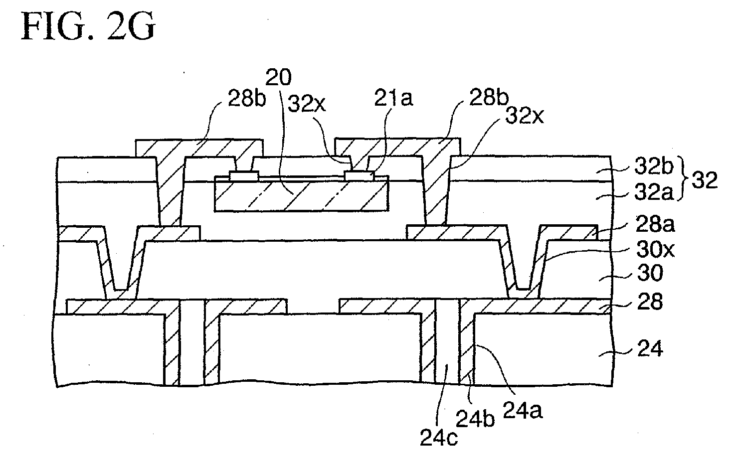
Description
- The present invention relates to an electronic parts packaging structure and a method of manufacturing the same, more particularly, an electronic parts packaging structure in which a semiconductor chip or the like is mounted on a wiring substrate in the state where the semiconductor chip or the like is buried in an insulation film, and a method of manufacturing the same.
- The development of LSI technology as a key technology to implement multimedia devices is proceeding steadily to a higher speed and a larger capacity of data transmission. According to this, a higher density of packaging technology as interfaces between LSI and electronic devices is also proceeding.
- Based on demands for further density growth, semiconductor devices in which a plurality of semiconductor chips are three-dimensionally stacked and mounted on a wiring substrate have been developed. To cite an example, each of Patent Literature 1 (Japanese Unexamined Patent Publication No. 2001-177045) and Patent Literature 2 (Japanese Unexamined Patent Publication No. 2000-323645) discloses a semiconductor device having a structure as follows: a plurality of semiconductor chips are three-dimensionally mounted on a wiring substrate in the state where the semiconductor chips are buried in insulation films, and the plurality of semiconductor chips are mutually connected using multilayered wiring patterns or the like formed with the insulation films interposed therebetween.
- However, in the above-described
Patent Literatures 1 and 2, there is no consideration for the fact that an interlayer insulation film is formed in the state where steps are generated due to the thickness of a semiconductor chip when the interlayer insulation film is formed on the mounted semiconductor chip. - Specifically, if steps are generated in the interlayer insulation film on the semiconductor chip, defocus is apt to occur in photolithography when wiring patterns are formed on the interlayer insulation film. Accordingly, it is difficult to form desired wiring patterns with high precision.
- Furthermore, since steps are also generated in the wiring patterns formed on the interlayer insulation film, reliability of bonding may be lowered when a semiconductor chip is flip-chip bonded to the wiring patterns.
- Accordingly, it is desirable to provide a method of manufacturing an electronic parts packaging structure which has a structure where an electronic parts is buried in an interlayer insulation film on a wiring substrate and in which steps due to the thickness of the electronic parts may be eliminated so that the electronic parts is planarized, and to provide the electronic parts packaging structure.
- According to an embodiment of the present invention, there is provided a method of manufacturing an electronic parts packaging structure, which includes the steps of: forming a first resin film uncured on a wiring substrate including a wiring pattern; burying an electronic parts having a connection terminal on an element formation surface in the first resin film uncured in a state where the connection terminal is directed upward; forming a second resin film for covering the electronic parts; obtaining an insulation film by curing the first and second resin films by heat treatment; forming a via hole in a predetermined portion of the insulation film on the wiring pattern and the connection terminal; and forming an upper wiring pattern connected to the wiring pattern and the connection terminal through the via hole, on the insulation film.
- In this embodiment of the present invention, first, the first resin film uncured is formed on the wiring substrate. Thereafter, the electronic parts (thinned semiconductor chip or the like) having the connection terminal on the element formation surface is pressed and buried in the first resin film in an uncured state, in the state where the connection terminal is directed upward. At this time, it is preferred that the element formation surface of the electronic parts and the upper surface of the first resin film are at almost the same height.
- Next, the second resin film uncured, which covers the electronic parts, is formed. Subsequently, the first and second resin films are cured by heat treatment, thus obtaining the insulation film. Then, the via hole is formed in the insulation film on the wiring pattern and the connection terminal, and the upper wiring pattern connected to the wiring pattern and the connection terminal through the via hole is formed on the insulation film.
- As described above, in an embodiment of the present invention, without adding any special planarization process, the electronic parts is buried in the insulation film to be mounted in the state where steps due to the thickness of the electronic parts are eliminated. This eliminates the possibility that defocus may occur in photolithography when the upper wiring pattern is formed above the electronic parts. Accordingly, the upper wiring pattern can be stably formed with high precision.
- Moreover, in the case where an upper electronic parts is flip-chip mounted on the upper wiring patterns above the electronic parts, reliability of the joint between upper electronic parts and the upper wiring patterns can be improved because the upper wiring patterns are placed at almost the same height over the entire wiring substrate.
- In the above-described embodiment, it is preferred that the first resin film is interposed between the backside of the electronic parts and the wiring substrate. Since the first resin film functions as an adhesive layer for adhering the electronic parts and the wiring substrate, the packaging structure is simplified, and reliability of the packaging structure can be improved.
- Further, in the case where an electronic parts including a passivation film having an opening portion for exposing the connection terminal is used as the electronic parts in the above-described embodiment, the second resin film may be omitted, and the upper wiring pattern is formed directly on the electronic parts.
- According to another embodiment of the present invention, there is provided a method of manufacturing an electronic parts packaging structure, which includes the steps of: forming a first resin film uncured on a wiring substrate including a wiring pattern; burying an electronic parts having a connection terminal on an element formation surface in the first resin film uncured in a state where the connection terminal is directed downward, and joining the connection terminal to the wiring pattern; forming a second resin film for covering the electronic parts; obtaining an insulation film by curing the first and second resin films by heat treatment; forming a via hole in a predetermined portion of the insulation film on the wiring pattern; and forming an upper wiring pattern connected to the wiring pattern through the via hole, on the insulation film.
- In this embodiment of the present invention, first, the first resin film uncured is formed on the wiring substrate. Thereafter, the electronic parts (thinned semiconductor chip or the like) is buried in the first resin film uncured, in the state where the connection terminal is directed downward, and the connection terminal of the electronic parts is flip-chip bonded to the wiring pattern. At this time, it is preferred that the backside of the electronic parts and the upper surface of the first resin film be adjusted so as to be at almost the same height.
- Next, after the second resin film for covering the electronic parts is formed, the first and second resin films are cured by heat treatment to become the insulation film. Then, after the via hole is formed in the insulation film on the wiring pattern, the upper wiring pattern connected to the wiring pattern through the via hole is formed on the insulation film.
- As described above, without adding any special planarization process, the electronic parts is buried in the insulation film in the state where steps due to the thickness of the electronic parts are eliminated, and the connection terminal of the electronic parts can be flip-chip bonded to the wiring pattern of the wiring substrate. Accordingly, the upper wiring pattern formed above the electronic parts can be formed with high precision. In addition, in the case where an upper electronic parts is flip-chip mounted on the upper wiring pattern, they are joined with high reliability.
- Moreover, since underfill resin does not need to be specially formed in the gap under the electronic parts, the cost of manufacture can be reduced.
- In the above-described embodiment of the present invention, the second resin film for covering the electronic parts may be omitted. In this case, particularly in the case where a thinned semiconductor chip is used as the electronic parts, it is preferred that the upper wiring pattern not be placed on the semiconductor chip for preventing a circuit pattern of the semiconductor chip and the upper wiring pattern from being short-circuited.
- Further, after the process of forming the resin film uncured, an opening portion may be formed in a predetermined portion of the resin film on the wiring pattern to which the connection terminal of the electronic parts is joined. In this case, the connection terminal of the electronic parts is joined to the wiring pattern while being placed so as to correspond to the opening portion of the resin film. In the case of this aspect, the possibility that resin may be interposed between the connection terminal of the electronic parts and the wiring pattern is eliminated. Accordingly, reliability of the electrical connection between the electronic parts and the wiring pattern can be improved.
- Reference will now be made, by way of example, to the accompanying drawings, in which:
- FIGS. 1A and 1B are sectional views showing disadvantageous points in the manufacture of a semiconductor device in which a semiconductor chip is mounted in the state of being buried in an insulation film;
- FIGS. 2A to 2H are sectional views showing a method of manufacturing an electronic parts packaging structure of a first embodiment of the present invention in order;
- FIGS. 3A to 3F are sectional views showing a method of manufacturing an electronic parts packaging structure of a second embodiment of the present invention in order;
- FIGS. 4A to 4D are sectional views showing a method of manufacturing an electronic parts packaging structure of a third embodiment of the present invention in order;
- FIGS. 5A to 5E are sectional views showing a method of manufacturing an electronic parts packaging structure of a fourth embodiment of the present invention in order; and
- FIGS. 6A to 6H are sectional views showing a method of manufacturing an electronic parts packaging structure of a fifth embodiment of the present invention in order.
-
- Hereinafter, embodiments of the present invention will be described with reference to the accompanying drawings.
- Before the present embodiments will be described, disadvantageous points in the manufacture of a semiconductor device in which a semiconductor chip is mounted in the state of being buried in an insulation film will be described. FIGS. 1A and 1B are sectional views showing the disadvantageous points in the manufacture of a semiconductor device in which a semiconductor chip is mounted in the state of being buried in an insulation film.
- As shown in FIG. 1A, first, a first
interlayer insulation film 102 is formed on abase substrate 100 including predetermined wiring patterns (not shown), and then aCu wiring 104 connected to the wiring patterns of thebase substrate 100 through via holes (not shown) formed in the firstinterlayer insulation film 102 is formed on the firstinterlayer insulation film 102. Asemiconductor chip 108 includingconnection terminals 108a is firmly fixed to theCu wiring 104 with anadhesive layer 106 interposed therebetween in the state where theconnection terminals 108a are directed upward. - Subsequently, a second
interlayer insulation film 110 is formed on thesemiconductor chip 108 and theCu wiring 104. At this time, the secondinterlayer insulation film 110 is formed in the state where it rises higher on thesemiconductor chip 108 than on theCu wiring 104 due to steps of thesemiconductor chip 108. - Then, as shown in FIG. 1B, via
holes 112 are formed by etching the secondinterlayer insulation film 110 on theconnection terminals 108a and the like of thesemiconductor chip 108 with a laser or the like. Subsequently, after a seed Cu film (not shown) is formed on the inner surfaces of thevia holes 112 and on the secondinterlayer insulation film 110, a resist film (not shown) in which portions where wiring patterns are to be formed are opened is formed by photolithography. - Next, after a Cu film pattern is formed in opening portions of the resist film pattern by electroplating in which the seed Cu film is utilized as a plating power-supply layer, the resist film is removed. Subsequently, the seed Cu film is etched using the Cu film pattern as a mask, thus obtaining the
wiring patterns 114. - Since steps are generated on the upper surface of the second
interlayer insulation film 110 under the influence of thesemiconductor chip 108, defocus is apt to occur in photolithography when the aforementioned resist film pattern is formed. Accordingly, troubles are apt to occur in the resist film pattern formed on the secondinterlayer insulation film 110. Therefore, it is difficult to form thewiring patterns 114 desired, with high precision. - Subsequently, bumps 116a of the
semiconductor chip 116 including thebumps 116a are flip-chip bonded toconnection portions 114a of thewiring patterns 114. At this time, since the heights of theconnection portions 114a of thewiring patterns 114 vary due to the steps of the secondinterlayer insulation film 110, bonding failures between thebumps 116a of thesemiconductor chip 116 and theconnection portions 114a of thewiring patterns 114 are apt to occur. - Electronic parts packaging structures of embodiments of the present invention and methods of manufacturing the same, described below, can solve the above-described problems.
- Next, a method of manufacturing an electronic parts packaging structure of a first embodiment of the present invention will be described. FIGS. 2A to 2H are sectional views showing a method of manufacturing the electronic parts packaging structure of the first embodiment of the present invention in order. In the method of manufacturing the electronic parts packaging structure of the first embodiment, as shown in FIG. 2A, first, a
base substrate 24 for manufacturing a build-up wiring substrate is prepared. Thebase substrate 24 is made of insulative material such as resin. Moreover, through-holes 24a are provided in thebase substrate 24, and through-hole plating layers 24b connected tofirst wiring patterns 28 on thebase substrate 24 are formed on the inner surfaces of the through-holes 24a. Holes of the through-hole plating layers 24b are filled withresin 24c. - Thereafter, a first
interlayer insulation film 30 made of resin or the like, which covers thefirst wiring patterns 28, is formed. Then, predetermined portions of the firstinterlayer insulation film 30 on thefirst wiring patterns 28 are etched by a laser, RIE, or the like, thereby forming first viaholes 30x. - Subsequently,
second wiring patterns 28a connected to thefirst wiring patterns 28 through the first viaholes 30x are formed on the firstinterlayer insulation film 30. Thesecond wiring patterns 28a are formed by a similar method to that of forming third wiring patterns to be described later. - Next, as shown in FIG. 2B, a
first resin film 32a is formed on thesecond wiring patterns 28a and the firstinterlayer insulation film 30. As thefirst resin film 32a, epoxy series resin, polyimide series resin, polyphenylene ether series resin, or the like is used. Methods of forming thefirst resin film 32a include a method of laminating a resin film and a method of forming a resin film by spin coating or printing. - In general, a resin film is formed by curing uncured resin material by heat treatment. However, one feature of the present embodiment is that a semiconductor chip is buried in a soft resin film in an uncured state. Accordingly, in this step, the
first resin film 32a is formed in an uncured state. That is, after resin material as described above is formed, the resin material is baked at 50 to 100 °C in order to be stuck tentatively, thus forming thefirst resin film 32a uncured. - The thickness of the
first resin film 32a is not particularly limited because it is set in consideration of the thickness of a semiconductor chip to be buried therein. However, the thickness of thefirst resin film 32a is preferably set to approximately twice the thickness of the semiconductor chip. - Subsequently, a semiconductor chip 20 (electronic parts) as shown in FIG. 2C is prepared.
Connection pads 21a (connection terminals) are exposed on the element formation surface of thesemiconductor chip 20, and the other part of thesemiconductor chip 20 is covered with apassivation film 21b. In order to obtain thissemiconductor chip 20, first, a semiconductor wafer which has a thickness of approximately 400 µm and which includes elements, such as transistors, and theconnection pads 21a connected to the elements on the element formation surface is prepared. Thereafter, the backside of the semiconductor wafer is ground and thinned to a thickness of approximately 150 µm (preferably, approximately 50 µm) or less, and then the semiconductor wafer is diced, thus obtainingindividual semiconductor chips 20. - Although the
semiconductor chip 20 is taken as an example of an electronic parts, various kinds of electronic parts including capacitor parts can be used. - Thereafter, as shown in FIG. 2C, the
semiconductor chip 20 is placed on thefirst resin film 32a with the element formation surface up (face up), and then thesemiconductor chip 20 is pressed, thereby excluding thefirst resin film 32a uncured to bury thesemiconductor chip 20 therein. At this time, thesemiconductor chip 20 is buried in thefirst resin film 32a so that the element formation surface of thesemiconductor chip 20 and the upper surface of thefirst resin film 32a may be at almost the same height. This eliminates the occurrence of steps due to the thickness of thesemiconductor chip 20 and makes it possible to achieve planarization without specially adding a planarization process. - Note that, of course, the height of the element formation surface of the
semiconductor chip 20 and that of the upper surface of thefirst resin film 32a may be different from each other to a degree in which photolithography and the like in subsequent steps are not adversely affected. - FIG. 2C illustrates a mode in which the
semiconductor chip 20 having a thickness of approximately 30 µm is buried in thefirst resin film 32a having a thickness of approximately 60 µm so that the upper surfaces thereof may be at almost the same height. Thus, in the present embodiment, it is preferred that thefirst resin film 32a is interposed between the backside of thesemiconductor chip 20 and the first interlayer insulation film 30 (or thesecond wiring patterns 28a) below thesemiconductor chip 20. - This is because the
first resin film 32a interposed between the backside of thesemiconductor chip 20 and the firstinterlayer insulation film 30 functions as an adhesive layer for adhering thesemiconductor chip 20 and the firstinterlayer insulation film 30. Thus, the present embodiment also has the advantage that the step of forming an adhesive layer on the backside of thesemiconductor chip 20 can be omitted, and is convenient from the viewpoint that the cost of manufacture can be reduced. - Incidentally, the
semiconductor chip 20 may be buried in thefirst resin film 32a so that the backside of thesemiconductor chip 20 may come into contact with the firstinterlayer insulation film 30 or thefirst wiring patterns 28a by adjusting the thicknesses of thesemiconductor chip 20 and thefirst resin film 32a. Also in this case, it is preferred that the element formation surface of thesemiconductor chip 20 and the upper surface of thefirst resin film 32a are at almost the same height. - Next, as shown in FIG. 2D, a
second resin film 32b uncured which covers thesemiconductor chip 20 is formed. Thesecond resin film 32b is formed by using material and a forming method similar to those of thefirst resin film 32a. The steps of the element formation surface due to thesemiconductor chip 20 are planarized by covering thesemiconductor chip 20 with thesecond resin film 32b. - Since the
semiconductor chip 20 is buried in thefirst resin film 32a to be mounted as described above, thesecond resin film 32b cannot be formed in the state where it locally rises on thesemiconductor chip 20, but formed in the state where it is planarized over all. - Subsequently, the structure of FIG. 2D is heat-treated at a temperature of 130 to 200 °C, thereby simultaneously curing the first and
second resin films second resin films second resin film 32b is cured in the state where the upper surface thereof is further planarized. - In this way, a second
interlayer insulation film 32 composed of thefirst resin film 32a (first insulating film) and thesecond resin film 32b (second insulation film) is obtained. - Next, as shown in FIG. 2E, predetermined portions of the second
interlayer insulation film 32 on theconnection pads 21a of thesemiconductor chip 20 and on thesecond wiring patterns 28a are etched by a laser, RIE, or the like, thereby forming second viaholes 32x. - Thereafter, as shown in FIG. 2F, a
seed Cu film 28x is formed on the inner surfaces of the second viaholes 32x and on the secondinterlayer insulation film 32. Then, a resistfilm 29 which has openingportions 29a corresponding to the third wiring patterns is formed by photolithography. At this time, since the secondinterlayer insulation film 32 is formed in the state where the upper surface thereof is planarized over all, defocus does not occur in photolithography. Accordingly, the resistfilm 29 having a predetermined pattern can be stably formed with high precision. - Subsequently, again as shown in FIG. 2F, by using the resist
film 29 as a mask, aCu film pattern 28y is formed by electroplating in which theseed Cu film 28x is utilized as a plating power-supply layer. - Then, after the resist
film 29 is removed, theseed Cu film 28x is etched by using theCu film pattern 28y as a mask. Thus, as shown in FIG. 2G, thethird wiring patterns 28b (upper wiring patterns), which are connected to theconnection pads 21a of thesemiconductor chip 20 and to thesecond wiring patterns 28a through the second viaholes 32x, are formed on the secondinterlayer insulation film 32. - Since the upper surface of the second
interlayer insulation film 32, which covers thesemiconductor chip 20, is made planar as described above, a focus margin need not be set large in photolithography when thethird wiring patterns 28b are formed on the secondinterlayer insulation film 32. Therefore, the resistfilm 29, which has the opening portions corresponding to thethird wiring patterns 28b, can be stably formed with high precision. Accordingly, thethird wiring patterns 28b desired can be obtained. - Note that the second and
third wiring patterns - Moreover, though not shown in figures, a mode in which a plurality of
semiconductor chips 20 are mutually connected in the state where they are buried in respective interlayer insulation films to be multilayered, may be adopted by repeating the process from the step (FIG. 2B) of forming thefirst resin film 32a to the step (FIG. 2G) of forming thethird wiring patterns 28b with a predetermined number of times. Also in such a case, each interlayer insulation film is formed in a planarized state. Accordingly, interlayer insulation films having semiconductor chips therein and wiring patterns can be formed in a stacking manner without any trouble. - Further, a mode in which semiconductor chips 20 are similarly buried in arbitrary interlayer insulation films among the plurality of interlayer insulation films may also be adopted. Furthermore, a mode in which a
semiconductor chip 20 is also stacked on the backside of thebase substrate 24 in the state where thesemiconductor chip 20 is buried in an interlayer insulation film may also be adopted. - Next, as shown in FIG. 2H, a solder resist
film 36 havingopening portions 36a onconnection portions 28z of thethird wiring patterns 28b, is formed. Then, theconnection portions 28z of thethird wiring patterns 28b are plated with Ni/Au. - Subsequently, an
upper semiconductor chip 20x (upper electronic parts) havingbumps 23 is prepared, and thebumps 23 of theupper semiconductor chip 20x are flip-chip bonded to theconnection portions 28z of thethird wiring patterns 28b. - At this time, since the
connection portions 28z of thethird wiring patterns 28b are placed at almost the same height without variation in height in a region above thesemiconductor chip 20 and in a region where thesemiconductor chip 20 does not exist, thebumps 23 of theupper semiconductor chip 20x can be joined to theconnection portions 28z with high reliability. - Note that the following may be adopted: bumps are formed by mounting solder balls, etc. on the opening
portions 36a of the solder resist 36, and connection terminals of theupper semiconductor chip 20x are joined to these bumps. - In this way, a semiconductor device 1 (electronic parts packaging structure) of the first embodiment of the present invention is completed.
- In the
semiconductor device 1 of the first embodiment, the first and secondinterlayer insulation films third wiring patterns 28 to 28b are formed on thebase substrate 24 in a stacking manner. Moreover, thesemiconductor chip 20 is mounted in the state of being buried face up in a central portion of the secondinterlayer insulation film 32. - That is, the
semiconductor chip 20 is mounted in the state where it is not in contact with the first interlayer insulation film 30 (or thesecond wiring patterns 28a) below thesemiconductor chip 20, and the secondinterlayer insulation film 32 is interposed between thesemiconductor chip 20 and the firstinterlayer insulation film 30. The secondinterlayer insulation film 32 interposed between the backside of thesemiconductor chip 20 and the firstinterlayer insulation film 30 also has a function of an adhesive layer for adhering these. As described above, an adhesive layer does not have to be specially provided on the backside of thesemiconductor chip 20. Accordingly, the structure of thesemiconductor device 1 can be simplified, and the reliability thereof can be improved. - Moreover, the
connection pads 21a of thesemiconductor chip 20 are electrically connected through thethird wiring patterns 28b to theupper semiconductor chip 20x and the like mounted above thesemiconductor chip 20. - In the method of manufacturing the
semiconductor device 1 of the present embodiment, since thesemiconductor chip 20 is mounted in the state of being buried in thefirst resin film 32a, thesecond resin film 32b formed on thesemiconductor chip 20 is formed in a planar state without being affected by the steps due to the thickness of thesemiconductor chip 20. Thus, thethird wiring patterns 28b formed on the secondinterlayer insulation film 32 are stably formed with high precision. - Further, in the first embodiment, the
third wiring patterns 28b are formed on thesecond resin film 32b covering thesemiconductor chip 20. Accordingly, even in the case where a film providing low reliability of insulation resistance is used as thepassivation film 21b of thesemiconductor chip 20, the possibility that thethird wiring patterns 28b and circuit patterns of thesemiconductor chip 20 may be electrically short-circuited is eliminated, thus making it possible to improve the reliability of thesemiconductor device 1. - In addition, since the heights at which the
connection portions 28z of thethird wiring patterns 28b are placed are the same, coplanarity (degree of planarity) for the join between theconnection portions 28z of thethird wiring patterns 28b and thebumps 23 of theupper semiconductor chip 20x can be reduced. This makes it possible to prevent the occurrence of bonding failures (bridge, open, and the like) between theconnection portions 28z of thethird wiring patterns 28b and thebumps 23 of theupper semiconductor chip 20x. - FIGS. 3A to 3F are sectional views showing a method of manufacturing an electronic parts packaging structure of a second embodiment of the present invention in order. The second embodiment is different from the first embodiment in that third wiring patterns are formed directly on a
semiconductor chip 20 without a second resin film being formed after the semiconductor chip is buried in a first resin film to be mounted. In the second embodiment, a detailed description of similar steps to those of the first embodiment will be omitted. - In the method of manufacturing the electronic parts packaging structure of the second embodiment, as shown in FIG. 3A, first, a
first resin film 32a uncured is formed on the firstinterlayer insulation films 30 and thesecond wiring patterns 28a on abase substrate 24 by a similar method to that of the first embodiment. - Thereafter, a
semiconductor chip 20a (electronic parts) as shown in FIG. 3B is prepared. Thissemiconductor chip 20a hasconnection pads 21a on an element formation surface thereof. On the other part of the element formation surface than theconnection pads 21a, apassivation film 21b (surface protection film) havingopening portions 21x for exposing theconnection pads 21a is provided. As thepassivation film 21b according to the second embodiment, one providing high reliability of insulation resistance is used. The material and thickness of such apassivation film 21b are not particularly limited. However, for example, thepassivation film 21b is composed of a silicon nitride film having a thickness of approximately 0.5 µm and a polyimide resin film having a thickness of approximately 3 µm or more. Alternatively, thepassivation film 21b may be formed by adhering a resin film exposing theconnection pads 21a, to thesemiconductor chip 20 used in the first embodiment. - The use of the
semiconductor chip 20a as described above eliminates the possibility that circuit patterns of thesemiconductor chip 20a and thethird wiring patterns 28b may be electrically short-circuited even if thethird wiring patterns 28a are formed directly on thesemiconductor chip 20a without a second resin film interposed therebetween, unlike the first embodiment. - Note that the material and structure of the passivation film of the semiconductor chip are appropriately selected in accordance with reliability specifications for various kinds of electronic parts packaging structures for preventing the circuit patterns of the
semiconductor chip 20a and thethird wiring patterns 28b from being short-circuited. - Next, again as shown in FIG. 3B, the
semiconductor chip 20a is buried in thefirst resin film 32a to be mounted by a similar method to that of the first embodiment. Thus, the element formation surface of thesemiconductor chip 20a and the upper surface of thefirst resin film 32a come to be at almost the same height. Accordingly, the occurrence of steps due to the thickness of thesemiconductor chip 20a is eliminated. - Subsequently, as shown in FIG. 3C, the structure of FIG. 3B is heat-treated at a temperature of 130 to 200 °C, whereby the
first resin film 32a is cured to be a secondinterlayer insulation film 32. Thereafter, predetermined portions of the secondinterlayer insulation film 32 on thesecond wiring patterns 28a are etched by a laser or RIE, thereby forming second viaholes 32x. - Then, as shown in FIG. 3D, the
third wiring patterns 28b (upper wiring patterns) are formed on the secondinterlayer insulation film 32 and thesemiconductor chip 20a by a semi-additive process or the like similarly to the first embodiment. Thethird wiring patterns 28b are connected to thesecond wiring patterns 28a through the second viaholes 32x and connected to theconnection pads 21a of thesemiconductor chip 20a through the openingportions 21x of thepassivation film 21b. - In the second embodiment, since the
third wiring patterns 28b can be formed directly on thesemiconductor chip 20a, the step of forming a second resin film on thesemiconductor chip 20a can be omitted. Accordingly, the number of steps in the manufacturing process is reduced compared to the first embodiment, thus making it possible to reduce the cost of manufacture. - Next, in the second embodiment, a mode in which fourth wiring patterns are further formed will be illustrated. That is, as shown in FIG. 3E, a third
interlayer insulation film 34, which is made of a resin film or the like and covers thethird wiring patterns 28b, is formed. Subsequently, predetermined portions of the thirdinterlayer insulation film 34 on thethird wiring patterns 28b are etched by a laser or RIE, thereby forming third viaholes 34x. Furthermore,fourth wiring patterns 28c connected to thethird wiring patterns 28b through the third viaholes 34x are formed by a semi-additive process or the like. - As described above, in the second embodiment, even in the case where a layer of wiring patterns are additionally formed, the number of steps can be reduced by one compared to the manufacturing method of the first embodiment. Accordingly, when electronic parts packaging structures having smaller sizes and higher performance are manufactured by increasing wiring densities, the cost of manufacture can be reduced more than the first embodiment.
- Next, as shown in FIG. 3F, a solder resist
film 36 havingopening portions 36a onconnection portions 28z of thefourth wiring patterns 28c, is formed similarly to the first embodiment. Thereafter, bumps 23 of anupper semiconductor chip 20x are flip-chip bonded to theconnection portions 28z of thefourth wiring patterns 28c. - In this way, a
semiconductor device 1a (electronic parts packaging structure) of the second embodiment is obtained. - Also in the second embodiment, modified examples similar to those of the first embodiment can be adopted.
- In the second embodiment, similar effects to those of the first embodiment are exerted. In addition, since wiring patterns can be formed directly on the
semiconductor chip 20a, the number of steps in the manufacturing process can be reduced by one compared to the manufacturing process of the first embodiment, thus making it possible to reduce the cost of manufacture. - FIGS. 4A to 4D are sectional views showing a method of manufacturing an electronic parts packaging structure of a third embodiment of the present invention in order. The third embodiment is different from the first embodiment in that a semiconductor chip is buried face down in a resin film to be flip-chip mounted. In the third embodiment, a detailed description of the same steps as those of the first embodiment will be omitted.
- In the method of manufacturing the electronic parts packaging structure of the third embodiment, as shown in FIG. 4A, first, a
resin film 32a uncured is formed on a firstinterlayer insulation film 30 andsecond wiring patterns 28a on abase substrate 24 by a similar method to that of the first embodiment. - Thereafter, a
semiconductor chip 20b (electronic parts) as shown in FIG. 4B is prepared. Thesemiconductor chip 20b hasconnection pads 21a and bumps 23 connected to theconnection pads 21a on an element formation surface, and is thinned to 150 µm (preferably, 50 µm) or less. Theconnection pads 21a and thebumps 23 connected thereto are examples of connection terminals. - Subsequently, again as shown in FIG. 4B, the
semiconductor chip 20b is placed on theresin film 32a in the state where the surface of thesemiconductor chip 20b on which thebumps 23 are mounted is directed downward (face down), and thesemiconductor chip 20 is pressed, thereby burying thesemiconductor chip 20b in theresin film 32a. Thus, thesemiconductor chip 20b excludes theresin film 32a, and thebumps 23 thereof come into contact with thesecond wiring patterns 28a. In addition, the backside of thesemiconductor chip 20b and the upper surface of theresin film 32a are at almost the same height to be planarized. - At this time, the thickness of the
semiconductor chip 20b and the thickness of theresin film 32a are appropriately adjusted so that the backside of thesemiconductor chip 20b and the upper surface of theresin film 32a may be at almost the same height. For example, in the case where the thickness of thesemiconductor chip 20b is approximately 30 µm and the heights of thebumps 23 are approximately 10 µm (total thickness: approximately 40 µm), theresin film 32a is formed so as to have a thickness of approximately 40 µm on thesecond wiring patterns 28a. - Next, the
bumps 23 of thesemiconductor chip 20b and thesecond wiring patterns 28a are joined. In the case where thebumps 23 of thesemiconductor chip 20b are made of Au, wirings having Au films on the surfaces thereof are used as thesecond wiring patterns 28a, and thebumps 23 of thesemiconductor chip 20b and thesecond wiring patterns 28a are joined by ultrasonic flip-chip mounting. - Alternatively, in the case where the
bumps 23 of thesemiconductor chip 20b are made of solder, Cu wirings or wirings having Au films on the surfaces thereof are used as thesecond wiring patterns 28a, and thebumps 23 of thesemiconductor chip 20b and thesecond wiring patterns 28a are joined by reflow heating. - Note that the portions of the
second wiring patterns 28a where thebumps 23 of thesemiconductor chip 20b are joined are plated with Ni/Au. - Thereafter, the
resin film 32a is cured by performing heat treatment at 130 to 200 °C, thus obtaining a secondinterlayer insulation film 32. - This provides a structure in which the
semiconductor chip 20b is buried in a planar state in the firstinterlayer insulation film 32 and in which thebumps 23 thereof are flip-chip bonded to thesecond wiring patterns 28a, as shown in FIG. 4B. - In the present embodiment, since the
semiconductor chip 20b is buried in theresin film 32a uncured to be flip-chip bonded to thesecond wiring patterns 28a, the gap under thesemiconductor chip 20b does not need to be filled with underfill resin but is filled with theresin film 32 which remains in the gap. Thus, the present embodiment also has the advantage that the step of filling the gap under thesemiconductor chip 20b with underfill resin is not particularly required. - Next, as shown in FIG. 4C, predetermined portions of the second
interlayer insulation film 32 on thesecond wiring patterns 28a are etched by a laser or RIE, thereby forming second viaholes 32x. - Subsequently,
third wiring patterns 28b (upper wiring patterns) connected to thesecond wiring patterns 28a through the second viaholes 32x are formed on the secondinterlayer insulation film 32 by a semi-additive process, which is described in the first embodiment, or the like. Also in the third embodiment, the backside of thesemiconductor chip 20b and the upper surface of the secondinterlayer insulation film 32 are at almost the same height to be planarized. Accordingly, the precision in photolithography when thethird wiring patterns 28b are formed can be improved. Thus, thethird wiring patterns 28b desired can be stably formed with high precision. - In the present embodiment, a mode in which a semiconductor chip thinned by grinding the backside thereof is used as the
semiconductor chip 20b is exemplified. Accordingly, thethird wiring patterns 28b are not formed on the backside of thesemiconductor chip 20b for preventing thethird wiring patterns 28b and circuit patterns of thesemiconductor chip 20b from being electrically short-circuited. Note that, in the case where an insulation film is formed on the backside of thesemiconductor chip 20b in advance, thethird wiring patterns 28b may be formed on the backside of thesemiconductor chip 20b. - In the third embodiment, similar to the first embodiment, a mode in which a plurality of
semiconductor chips 20b are mutually connected in the state where they are buried in respective interlayer insulation films to be multilayered, may also be adopted by repeating the process from the step (FIG. 4A) of forming thefirst resin film 32a to the step (FIG. 4C) of forming thethird wiring patterns 28b with a predetermined number of times. - Next, as shown in FIG. 4D, a solder resist
film 36 havingopening portions 36a onconnection portions 28z of thethird wiring patterns 28b is formed. Thereafter, bumps 23 of anupper semiconductor chip 20x (upper electronic parts) including thebumps 23 are flip-chip bonded to theconnection portions 28z of thethird wiring patterns 28b. Also in the third embodiment, since theconnection portions 28z of thethird wiring patterns 28b do not vary in height to be placed at almost the same height, thebumps 23 of theupper semiconductor chip 20x can be joined to theconnection portions 28z with high reliability. - In this way, a
semiconductor device 1b (electronic parts packaging structure) of the third embodiment is obtained. - In the method of manufacturing the electronic parts packaging structure of the third embodiment, the
semiconductor chip 20b is buried face down in theresin film 32a uncured, and thebumps 23 of thesemiconductor chip 20b are flip-chip bonded to thesecond wiring patterns 28a. - Thus, without adding a special planarization process, the
semiconductor chip 20b is buried in the secondinterlayer insulation film 32 in the state where steps due to the thickness of thesemiconductor chip 20b are eliminated, and is flip-chip bonded to the second wiring patterns. Accordingly, similar to the first embodiment, thethird wiring patterns 28b can be stably formed with high precision, and theupper semiconductor chip 20x can be flip-chip bonded to thethird wiring patterns 28b with high reliability. - Moreover, since the gap under the
semiconductor chip 20b does not need to be filled with underfill resin specially, there is the advantage that the cost of manufacture can be reduced. - FIGS. 5A to 5E are sectional views showing a method of manufacturing an electronic parts packaging structure of a fourth embodiment of the present invention in order. The fourth embodiment is different from the third embodiment in that after a semiconductor chip is mounted by a similar method to that of the third embodiment, an insulation film is formed on the semiconductor chip. This enables wiring patterns to be also formed in the region above the semiconductor chip. In the fourth embodiment, a detailed description of the same steps as those of the first and third embodiments will be omitted.
- In the method of manufacturing the electronic parts packaging structure of the fourth embodiment of the present invention, as shown in FIG. 5A, first, by a similar method to that of the third embodiment, a
semiconductor chip 20b (electronic parts) is buried face down in afirst resin film 32a uncured, and bumps 23 of thesemiconductor chip 20b are flip-chip bonded tosecond wiring patterns 28a. - Thereafter, as shown in FIG. 5B, a
second resin film 32b uncured, which covers thesemiconductor chip 20b, is formed. Subsequently, the first andsecond resin films second resin films interlayer insulation film 32 composed of the first andsecond resin films - Then, as shown in FIG. 5C, predetermined portions of the second
interlayer insulation film 32 on thesecond wiring patterns 28a are etched by a laser or RIE, thereby forming second viaholes 32x. - Subsequently, as shown in FIG. 5D,
third wiring patterns 28b (upper wiring patterns) connected to thesecond wiring patterns 28a through the second viaholes 32x are formed on the secondinterlayer insulation film 32 by a sub-additive process, which is described in the first embodiment, or the like. - The
semiconductor chip 20b used in the present embodiment is one thinned to 150 µm (preferably, 50 µm) or less by grinding the backside thereof, and a semiconductor (silicon) layer is exposed on the backside of thesemiconductor chip 20b. Therefore, in the case where thethird wiring patterns 28b are formed directly on the backside of thesemiconductor chip 20b, thethird wiring patterns 28b and circuit patterns of thesemiconductor chip 20b may be electrically short-circuited. Accordingly, in the aforementioned third embodiment, thethird wiring patterns 28b are not placed on thesemiconductor chip 20b. - However, in the fourth embodiment, as shown in FIG. 5D, the
second resin film 32b is provided on thesemiconductor chip 20b, and thethird wiring patterns 28b are formed on thesecond resin film 32b. Therefore, thethird wiring patterns 28b can also be placed in the region above thesemiconductor chip 20b. - That is, in the fourth embodiment, flexibility in designing the
third wiring patterns 28b can be increased compared to the third embodiment. Therefore, the wiring density of the electronic parts packaging structure can be increased, thus making it possible to easily cope with the trend toward smaller electronic parts packaging structures and that toward higher-performance ones. - Next, as shown in FIG. 5E, a solder resist
film 36 havingopening portions 36a onconnection portions 28z of thethird wiring patterns 28b is formed. Furthermore, bumps 23 of anupper semiconductor chip 20x (upper electronic parts) are flip-chip bonded to theconnection portions 28z of thethird wiring patterns 28b. - In this way, a
semiconductor device 1c (electronic parts packaging structure) of the fourth embodiment is obtained. - In the fourth embodiment, similar effects to those of the third embodiment are exerted. In addition, since the backside of the
semiconductor chip 20b is covered with the second interlayer insulation film 32 (thesecond resin film 32b), thethird wiring patterns 28b can also be formed above thesemiconductor chip 20b, thus making it possible to increase the wiring density. - FIGS. 6A to 6H are sectional views showing a method of manufacturing an electronic parts packaging structure of a fifth embodiment of the present invention in order. In the aforementioned third and fourth embodiments, bumps of a semiconductor chip are joined to wiring patterns while a resin film is being excluded. Accordingly, a small amount of resin may be interposed between the bumps of the semiconductor chip and the wiring patterns, and there may be cases where sufficient reliability of electrical connection cannot be obtained. In the fifth embodiment, such a trouble can be eliminated. Note that, in the fifth embodiment, a detailed description of the same steps as those of the first and third embodiments will be omitted.
- In the method of manufacturing the electronic parts packaging structure of the fifth embodiment, as shown in FIG. 6A, first, by a similar method to that of the first embodiment, a
first resin film 32a uncured is formed by, for example, adhering a resin film to a firstinterlayer insulation film 30 andsecond wiring patterns 28a on abase substrate 24. - Thereafter, as shown in FIG. 6B, portions of the
first resin film 32a on thesecond wiring patterns 28a to which bumps of a semiconductor chip are connected later are etched by a laser or the like, thereby forming openingportions 33 having depths reaching thesecond wiring patterns 28a. - At this time, the portions of the
second wiring patterns 28a to which thebumps 23 of thesemiconductor chip 20b are joined are plated with Ni/Au, and Ni/Au layers are exposed in the openingportions 33. Moreover, since the bumps of the semiconductor chip are placed in the openingportions 33 later, the diameters of the openingportions 33 are set equal to or more than the diameters of thebumps 23 of thesemiconductor chip 20b. - Next, as shown in FIG. 6C, the
semiconductor chip 20b (electronic parts) includingconnection pads 21a and thebumps 23 connected to theconnection pads 21a is prepared. Similar to the third embodiment, the thickness of thesemiconductor chip 20b is thinned to approximately 150 µm or less. - Then, the
semiconductor chip 20b is placed and pressed on thefirst resin film 32a so that thebumps 23 of thesemiconductor chip 20b may correspond to the portions of thesecond wiring patterns 28a which are exposed in the openingportions 33 of thefirst resin film 32a. Thus, thebumps 23 of thesemiconductor chip 20b are placed on thesecond wiring patterns 28a in contact therewith without excluding thefirst resin film 32a. - Subsequently, as shown in FIG. 6D, similar to the third embodiment, the
bumps 23 of thesemiconductor chip 20b are joined to thesecond wiring patterns 28a. As a joining method, ultrasonic flip-chip mounting is employed in the case where thebumps 23 of thesemiconductor chip 20b are made of Au, but flip-chip mounting by reflow heating at 200 to 250 °C is employed in the case where thebumps 23 of thesemiconductor chip 20b are made of solder. - Incidentally, when the
bumps 23 of thesemiconductor chip 20b are placed in the openingportions 33 of thefirst resin film 32a, a little gap remains between thesemiconductor chip 20b and the side surfaces of the openingportions 33 of thefirst resin film 32a. In the case where thermosetting resin is used for thefirst resin film 32a, the side surfaces of the openingportions 33 thereof are cured to a certain degree by heat when the openingportions 33 are formed by a laser. Accordingly, the embedding effect by reflowing thefirst resin film 32a is relatively small. Therefore, in the present embodiment, in the case where thebumps 23 of thesemiconductor chip 20b are solder bumps, thebumps 23 are reflowed and cured to be deformed, thereby filling the gap. Thereafter, thefirst resin film 32a is cured by performing heat treatment in an environment at a temperature of 130 to 200 °C. - Incidentally, to cite a modified example, the aforementioned gap may be filled by using, as the
first resin film 32a, light-curing resin having characteristics in which the light-curing resin reflows into the openingportions 33 when being cured by irradiation of ultraviolet light. This is because, in the case of light-curing resin, when the openingportions 33 are formed by a laser, the side surfaces thereof are not cured. - Moreover, in the case where solder is used for the
bumps 23 of thesemiconductor chip 20b, it is also possible to simultaneously cure thefirst resin film 32a by heat treatment when solder is reflowed and cured. - Thus, the
semiconductor chip 20b is flip-chip bonded to thesecond wiring patterns 28a in the state where thesemiconductor chip 20b is buried in thefirst resin film 32a. Further, similar to the third embodiment, the thickness of thefirst resin film 32a is adjusted in accordance with the thickness of thesemiconductor chip 20b. Accordingly, the backside of thesemiconductor chip 20b and the upper surface of thefirst resin film 32a are at almost the same height, thus eliminating steps due to thesemiconductor chip 20b. - Incidentally, the backside of the
semiconductor chip 20b and the upper surface of thefirst resin film 32a do not necessarily need to be set at the same height. In the case were a second resin film for covering thesemiconductor chip 20b is formed as described later, planarization may be completely achieved with the second resin film. - In the fifth embodiment, after the opening
portions 33 are formed in thefirst resin film 32a, thebumps 23 of thesemiconductor chip 20b are joined to thesecond wiring patterns 28a exposed in the openingportions 33. Accordingly, there is no possibility that resin may be interposed at the joint interface between thebumps 23 of thesemiconductor chip 20b and thesecond wiring patterns 28a. Therefore, thebumps 23 of thesemiconductor chip 20b are joined to thesecond wiring patterns 28b with high reliability, thus making it possible to obtain favorable electrical connection. - Subsequently, as shown in FIG. 6E, the
second resin film 32b is formed on thefirst resin film 32a and thesemiconductor chip 20b. Thus, a secondinterlayer insulation film 32 composed of the first andsecond resin films - Note that the following may be adopted: before the
first resin film 32a is cured, thesecond resin film 32b uncured is formed on thefirst resin film 32a, and then the first andsecond resin films - Next, as shown in FIG. 6F, predetermined portions of the second
interlayer insulation film 32 on thesecond wiring patterns 28a are etched by a laser or RIE, thereby forming second viaholes 32x. - Subsequently, as shown in FIG. 6H,
third wiring patterns 28b (upper wiring patterns) connected to thesecond wiring patterns 28a through the second viaholes 32x are formed on the secondinterlayer insulation film 32 by a semi-additive process, which is described in the first embodiment, or the like. - Incidentally, to cite a modified example, similar to the third embodiment, a mode in which the
second resin film 32b is not formed may be adopted. In this case, a similar structure to that of FIG. 4C is obtained, and thethird wiring patterns 28b are formed on thefirst resin film 32a except the region on thesemiconductor chip 20b. - Moreover, also in the fifth embodiment, a mode in which a plurality of
semiconductor chips 20b are mutually connected in the state where they are buried in respective interlayer insulation films to be multilayered, may be adopted by repeating the process from the step (FIG. 6A) of forming thefirst resin film 32a to the step (FIG. 6G) of forming thethird wiring patterns 28b with a predetermined number of times. - Subsequently, as shown in FIG. 6H, after a solder resist
film 36 havingopening portions 36a onconnection portions 28z of thethird wiring patterns 28b is formed, theconnection portions 28z of thethird wiring patterns 28b are plated with Ni/Au. Thereafter, bumps 23 of anupper semiconductor chip 20x (upper electronic parts) are flip-chip bonded to theconnection portions 28z of thethird wiring patterns 28b. Furthermore, the gap between theupper semiconductor chip 20x and the solder resistfilm 36 is filled with underfill resin as needed. - In this way, a
semiconductor device 1d (electronic parts packaging structure) of the fifth embodiment is obtained. - In the fifth embodiment, similar to other embodiments, without adding a special planarization process, the
semiconductor chip 20b is buried in the secondinterlayer insulation film 32 in the state where steps due to thesemiconductor chip 20b are eliminated, and is flip-chip bonded to thesecond wiring patterns 28a. Accordingly, similar to other embodiments, thethird wiring patterns 28b can be stably formed with high precision, and theupper semiconductor chip 20x can be flip-chip bonded to thethird wiring patterns 28b with high reliability. - Moreover, in the present embodiment, there is no need to form a non conductive paste (NCP) or a non conductive film (NCF) before the
semiconductor chip 20b is mounted, and there is no need to fill underfill resin after thesemiconductor chip 20b is mounted. That is, since thefirst resin film 32a in which thesemiconductor chip 20b is buried performs the role played by NCP or an NCF in previously-proposed techniques, the number of steps in the manufacturing process can be reduced, thereby making it possible to reduce the cost of manufacture. - In addition, the opening
portions 33 are previously formed in thefirst resin film 32a in which thesemiconductor chip 20b is to be buried, and thebumps 23 of thesemiconductor chip 20b are joined to the portions of thesecond wiring patterns 28a exposed in the openingportions 33. Thus, thebumps 23 of thesemiconductor chip 20b are electrically connected to thesecond wiring patterns 28a with higher reliability than the third or fourth embodiment, and the manufacturing yield ofsemiconductor devices 1d can be improved.
Claims (17)
- A method of manufacturing an electronic parts packaging structure, comprising the steps of:forming a first resin film uncured (32a) on a wiring substrate (24) including a wiring pattern (28a);burying an electronic parts (20) having a connection terminal (21a) on an element formation surface in the first resin film uncured (32a) in a state where the connection terminal (21a) is directed upward;forming a second resin film (32b) for covering the electronic parts (20);obtaining an insulation film (32) by curing the first and second resin films (32a, 32b) by heat treatment;forming a via hole (32x) in a predetermined portion of the insulation film (32) on the wiring pattern (28a) and the connection terminal (21a); andforming an upper wiring pattern (28b) connected to the wiring pattern (28a) and the connection terminal (21a) through the via hole (32x), on the insulation film (32).
- A method of manufacturing an electronic parts packaging structure, comprising the steps of:forming a resin film uncured (32a) on a wiring substrate (24) including a wiring pattern (28a);burying an electronic parts (20a), which has a connection terminal (21a) and a passivation film (21b) having an opening portion (21x) for exposing the connection terminal (21a) on an element formation surface, in the resin film uncured (32a) in a state where the connection terminal (21a) is directed upward;obtaining an insulation film (32) by curing the resin film (32a) by heat treatment;forming a via hole (32x) in a predetermined portion of the insulation film (32) on the wiring pattern (28a); andforming an upper wiring pattern (28a), which is connected to the wiring pattern (28a) through the via hole (32x) and connected to the connection terminal (21a) through the opening portion (21x), on the insulation film (32) and the electronic parts (20a).
- A method of manufacturing an electronic parts packaging structure, comprising the steps of:forming a resin film uncured (32a) on a wiring substrate (24) including a wiring pattern (28a);burying an electronic parts (20b) having a connection terminal (23) on an element formation surface in the resin film uncured (32a) in a state where the connection terminal (23) is directed downward, and joining the connection terminal (23) to the wiring pattern (28a);obtaining an insulation film (32) by curing the resin film (32a) by heat treatment;forming a via hole (32x) in a predetermined portion of the insulation film (32) on the wiring pattern (28a); andforming an upper wiring pattern (28b) connected to the wiring pattern (28a) through the via hole (32x), on the insulation film (32).
- A method of manufacturing an electronic parts packaging structure, comprising the steps of:forming a first resin film uncured (32a) on a wiring substrate (24) including a wiring pattern (28a);burying an electronic parts (20b) having a connection terminal (23) on an element formation surface in the first resin film uncured (28a) in a state where the connection terminal (23) is directed downward, and joining the connection terminal (23) to the wiring pattern (28a);forming a second resin film (32b) for covering the electronic parts (20b);obtaining an insulation film (32) by curing the first and second resin films (32a, 32b) by heat treatment;forming a via hole (32x) in a predetermined portion of the insulation film (32) on the wiring pattern (28a); andforming an upper wiring pattern (28b) connected to the wiring pattern (28a) through the via hole (32x), on the insulation film (32).
- The method according to claim 3 or 4, after the step of forming the resin film uncured (32a) and before the step of joining the connection terminal (23) of the electronic parts (20b) to the wiring pattern (28a), further comprising the step of:wherein the step of joining the connection terminal (23) of the electronic parts (20b) to the wiring pattern (28a) includes placing the connection terminal (23) of the electronic parts (20b) while making the connection terminal (23) of the electronic parts (20b) correspond to the opening portion (33) of the resin film.forming an opening portion (33) in a portion of the resin film (32a) on the wiring pattern (28a) to which the connection terminal (23) of the electronic parts (20b) is joined,
- The method according to claim 5,
wherein the connection terminal (23) of the electronic parts (20b) is a solder bump, and
wherein in the step of joining the connection terminal (23) of the electronic parts (20b) to the wiring pattern (28a), a gap between the electronic parts (20b) and a side surface of the opening portion (33) of the resin film (32a) is filled by deforming the solder bump by reflowing and curing. - The method according to any preceding claim, wherein in the step of burying the electronic parts (20, 20a, 20b) in the resin film uncured (32a), an upper surface of the resin film uncured (32a) and any one of the element formation surface and a backside of the electronic parts (20, 20a, 20b) are set at an almost same height.
- The method according to any one of claims 1 or 2, wherein in the step of burying the electronic parts (20) in the resin film uncured (32a), the resin film (32a) is interposed between a backside of the electronic parts (20, 20a) and the wiring substrate (24).
- The method according to claim 3, wherein in the step of forming the upper wiring pattern (28b), the upper wiring pattern (28b) is not formed on the electronic parts (20b).
- The method according to any preceding claim, further comprising the step of: repeating the steps from the step of burying the electronic parts (20, 20a, 20b) in the resin film (32a) to the step of forming the upper wiring pattern (28b) a predetermined number of times.
- The method according to any preceding claim, further comprising the step of, flip-chip bonding an upper electronic parts (20x) to the upper wiring pattern (28b).
- The method according to any preceding claim, wherein the electronic parts (20, 20a, 20b) is a semiconductor chip having a thickness of approximately 150 µm or less.
- An electronic parts packaging structure comprising:a wiring substrate (24) including a wiring pattern (28a);a first insulation film (32a) formed on the wiring substrate (24);an electronic parts (20) having a connection terminal (21a) on an element formation surface, the electronic parts (20) being buried in the first insulation film (32a) in a state where the connection terminal (21a) is directed upward and being mounted in a state where a backside of the electronic parts (20) is not in contact with the wiring substrate (24);a second insulation film (32b) for covering the electronic parts (20);via holes (32x) respectively formed in a predetermined portion of the first and second insulation films (32a,32b) on the wiring pattern (28a) and the connection terminal (21a); andan upper wiring pattern (28b) formed on the second insulation film (32b), the upper wiring pattern (28b) being connected to the wiring pattern (28a) and the connection terminal (21a) through the via holes (32x).
- An electronic parts packaging structure comprising:a wiring substrate (24) including a wiring pattern (28a);an insulation film (32) formed on the wiring substrate (24);an electronic parts (20a) including a connection terminal (21a) and a passivation film (21b) having an opening portion (21x) for exposing the connection terminal (21a) on an element formation surface, the electronic parts (20a) being buried in the insulation film (32) in a state where the connection terminal (21a) is directed upward and being mounted in a state where a backside of the electronic parts (20a) is not in contact with the wiring substrate (24);a via hole (32x) formed in a predetermined portion of the insulation film (32) on the wiring pattern (28a); andan upper wiring pattern (28b) formed on the insulation film (32) and the electronic parts (20a), the upper wiring pattern (28b) being connected to the wiring pattern (28a) through the via hole (32x) and connected to the connection terminal (21a) through the opening portion (21x).
- The electronic parts packaging structure according to any one of claims 13 or 14, wherein the element formation surface of the electronic parts (20, 20a) and an upper surface of the insulation film (32) in which the electronic parts (20, 20a) is buried are at an almost same height to be planarized.
- The electronic parts packaging structure according to any one of claims 13, 14 or 15, wherein the electronic parts (20, 20a) is a semiconductor chip having a thickness of approximately 150 µm or less.
- The electronic parts packaging structure according to any one of claims 13 to 16, wherein the insulation film (32) is made of resin.
Priority Applications (1)
| Application Number | Priority Date | Filing Date | Title |
|---|---|---|---|
| EP05015323.8A EP1615264B1 (en) | 2003-01-23 | 2004-01-23 | Method of manufacturing an electronic parts packaging structure |
Applications Claiming Priority (4)
| Application Number | Priority Date | Filing Date | Title |
|---|---|---|---|
| JP2003014588 | 2003-01-23 | ||
| JP2003014588 | 2003-01-23 | ||
| JP2003386398 | 2003-11-17 | ||
| JP2003386398A JP4489411B2 (en) | 2003-01-23 | 2003-11-17 | Manufacturing method of electronic component mounting structure |
Related Child Applications (2)
| Application Number | Title | Priority Date | Filing Date |
|---|---|---|---|
| EP05015323.8A Division EP1615264B1 (en) | 2003-01-23 | 2004-01-23 | Method of manufacturing an electronic parts packaging structure |
| EP05015323.8 Division-Into | 2005-07-14 |
Publications (3)
| Publication Number | Publication Date |
|---|---|
| EP1441389A2 true EP1441389A2 (en) | 2004-07-28 |
| EP1441389A3 EP1441389A3 (en) | 2004-08-04 |
| EP1441389B1 EP1441389B1 (en) | 2012-01-04 |
Family
ID=32599342
Family Applications (2)
| Application Number | Title | Priority Date | Filing Date |
|---|---|---|---|
| EP04250386A Expired - Fee Related EP1441389B1 (en) | 2003-01-23 | 2004-01-23 | Method of manufacturing an electronic parts packaging structure |
| EP05015323.8A Expired - Fee Related EP1615264B1 (en) | 2003-01-23 | 2004-01-23 | Method of manufacturing an electronic parts packaging structure |
Family Applications After (1)
| Application Number | Title | Priority Date | Filing Date |
|---|---|---|---|
| EP05015323.8A Expired - Fee Related EP1615264B1 (en) | 2003-01-23 | 2004-01-23 | Method of manufacturing an electronic parts packaging structure |
Country Status (6)
| Country | Link |
|---|---|
| US (3) | US7285862B2 (en) |
| EP (2) | EP1441389B1 (en) |
| JP (1) | JP4489411B2 (en) |
| KR (1) | KR101046265B1 (en) |
| CN (1) | CN1518080A (en) |
| TW (1) | TWI326913B (en) |
Cited By (3)
| Publication number | Priority date | Publication date | Assignee | Title |
|---|---|---|---|---|
| AT503718B1 (en) * | 2004-08-05 | 2009-06-15 | Imbera Electronics Oy | PREPARATION OF A LAYER COMPRISING A COMPONENT |
| US8609539B2 (en) | 2005-11-02 | 2013-12-17 | Canon Kabushiki Kaisha | Embedded semiconductor device substrate and production method thereof |
| CN112151433A (en) * | 2019-06-27 | 2020-12-29 | 何崇文 | Substrate structure, packaging structure and manufacturing method thereof |
Families Citing this family (49)
| Publication number | Priority date | Publication date | Assignee | Title |
|---|---|---|---|---|
| US9691635B1 (en) | 2002-05-01 | 2017-06-27 | Amkor Technology, Inc. | Buildup dielectric layer having metallization pattern semiconductor package fabrication method |
| US7548430B1 (en) | 2002-05-01 | 2009-06-16 | Amkor Technology, Inc. | Buildup dielectric and metallization process and semiconductor package |
| JP3920195B2 (en) * | 2002-11-11 | 2007-05-30 | 新光電気工業株式会社 | Electronic component mounting structure and manufacturing method thereof |
| US10811277B2 (en) | 2004-03-23 | 2020-10-20 | Amkor Technology, Inc. | Encapsulated semiconductor package |
| US11081370B2 (en) | 2004-03-23 | 2021-08-03 | Amkor Technology Singapore Holding Pte. Ltd. | Methods of manufacturing an encapsulated semiconductor device |
| US20050258533A1 (en) * | 2004-05-21 | 2005-11-24 | Matsushita Electric Industrial Co., Ltd. | Semiconductor device mounting structure |
| JP2006019441A (en) * | 2004-06-30 | 2006-01-19 | Shinko Electric Ind Co Ltd | Method of manufacturing substrate with built-in electronic substrate |
| US7615856B2 (en) * | 2004-09-01 | 2009-11-10 | Sanyo Electric Co., Ltd. | Integrated antenna type circuit apparatus |
| TWI256694B (en) * | 2004-11-19 | 2006-06-11 | Ind Tech Res Inst | Structure with embedded active components and manufacturing method thereof |
| US20090008792A1 (en) * | 2004-11-19 | 2009-01-08 | Industrial Technology Research Institute | Three-dimensional chip-stack package and active component on a substrate |
| CN101826496B (en) | 2005-05-23 | 2015-03-18 | 揖斐电株式会社 | Printed wiring board and manufacturing method thereof |
| JP2006332094A (en) | 2005-05-23 | 2006-12-07 | Seiko Epson Corp | Process for producing electronic substrate, process for manufacturing semiconductor device and process for manufacturing electronic apparatus |
| JP4533248B2 (en) * | 2005-06-03 | 2010-09-01 | 新光電気工業株式会社 | Electronic equipment |
| CN100372111C (en) * | 2005-09-09 | 2008-02-27 | 威盛电子股份有限公司 | Embedded packaging structure and its packaging method |
| JP4593444B2 (en) * | 2005-11-07 | 2010-12-08 | 新光電気工業株式会社 | Manufacturing method of electronic component mounting structure |
| FI119729B (en) * | 2005-11-23 | 2009-02-27 | Vti Technologies Oy | A method of making a microelectromechanical component and a microelectromechanical component |
| KR100827315B1 (en) | 2006-09-19 | 2008-05-06 | 삼성전기주식회사 | Manufacturing method of electronic chip embedded printed circuit board |
| TWI353661B (en) * | 2007-04-09 | 2011-12-01 | Unimicron Technology Corp | Circuit board structure capable of embedding semic |
| KR100837281B1 (en) * | 2007-05-23 | 2008-06-11 | 삼성전자주식회사 | Semiconductor device package and method of fabricating the same |
| JP5012896B2 (en) * | 2007-06-26 | 2012-08-29 | 株式会社村田製作所 | Manufacturing method of component-embedded substrate |
| TWI348213B (en) * | 2007-08-15 | 2011-09-01 | Packaging substrate structure with capacitor embedded therein and method for fabricating the same | |
| US7759212B2 (en) * | 2007-12-26 | 2010-07-20 | Stats Chippac, Ltd. | System-in-package having integrated passive devices and method therefor |
| US8093704B2 (en) * | 2008-06-03 | 2012-01-10 | Intel Corporation | Package on package using a bump-less build up layer (BBUL) package |
| KR101486420B1 (en) | 2008-07-25 | 2015-01-26 | 삼성전자주식회사 | Chip package and stacked package using the same and method of fabricating them |
| FR2938976A1 (en) * | 2008-11-24 | 2010-05-28 | St Microelectronics Grenoble | SEMICONDUCTOR DEVICE WITH STACKED COMPONENTS |
| WO2010095208A1 (en) * | 2009-02-17 | 2010-08-26 | 株式会社 村田製作所 | Module with built-in component and method for manufacturing the module |
| US9299648B2 (en) * | 2009-03-04 | 2016-03-29 | Stats Chippac Ltd. | Integrated circuit packaging system with patterned substrate and method of manufacture thereof |
| US8796561B1 (en) * | 2009-10-05 | 2014-08-05 | Amkor Technology, Inc. | Fan out build up substrate stackable package and method |
| US8937381B1 (en) | 2009-12-03 | 2015-01-20 | Amkor Technology, Inc. | Thin stackable package and method |
| US8237272B2 (en) | 2010-02-16 | 2012-08-07 | Taiwan Semiconductor Manufacturing Company, Ltd. | Conductive pillar structure for semiconductor substrate and method of manufacture |
| US8222726B2 (en) * | 2010-03-29 | 2012-07-17 | Advanced Semiconductor Engineering, Inc. | Semiconductor device package having a jumper chip and method of fabricating the same |
| JP2011243790A (en) | 2010-05-19 | 2011-12-01 | Panasonic Electric Works Co Ltd | Wiring method, structure provided wiring on surface, semiconductor device, wiring board, memory card, electric device, module, and multilayer circuit board |
| TWI508245B (en) * | 2010-10-06 | 2015-11-11 | 矽品精密工業股份有限公司 | Package of embedded chip and manufacturing method thereof |
| CN102456636B (en) * | 2010-10-19 | 2015-10-14 | 矽品精密工业股份有限公司 | The manufacture method of the packaging part of embedded chip |
| US9721984B2 (en) * | 2012-04-12 | 2017-08-01 | Taiwan Semiconductor Manufacturing Company, Ltd. | Image sensor manufacturing methods |
| CN103906370B (en) * | 2012-12-27 | 2017-01-11 | 碁鼎科技秦皇岛有限公司 | Chip packaging structure, circuit board having embedded component and manufacturing method thereof |
| US9655253B2 (en) * | 2013-07-25 | 2017-05-16 | Cyntec Co., Ltd. | Method of fabrication of encapsulated electronics devices mounted on a redistribution layer |
| US9466581B2 (en) | 2013-10-18 | 2016-10-11 | Taiwan Semiconductor Manufacturing Company Ltd. | Semiconductor package device and manufacturing method thereof |
| US9673171B1 (en) | 2014-03-26 | 2017-06-06 | STATS ChipPAC Pte. Ltd. | Integrated circuit packaging system with coreless substrate and method of manufacture thereof |
| US9202803B2 (en) * | 2014-03-28 | 2015-12-01 | Intel Corporation | Laser cavity formation for embedded dies or components in substrate build-up layers |
| US9721799B2 (en) | 2014-11-07 | 2017-08-01 | Advanced Semiconductor Engineering, Inc. | Semiconductor package with reduced via hole width and reduced pad patch and manufacturing method thereof |
| US10079156B2 (en) | 2014-11-07 | 2018-09-18 | Advanced Semiconductor Engineering, Inc. | Semiconductor package including dielectric layers defining via holes extending to component pads |
| US9420695B2 (en) | 2014-11-19 | 2016-08-16 | Advanced Semiconductor Engineering, Inc. | Semiconductor package structure and semiconductor process |
| US9426891B2 (en) | 2014-11-21 | 2016-08-23 | Advanced Semiconductor Engineering, Inc. | Circuit board with embedded passive component and manufacturing method thereof |
| JP2018018936A (en) * | 2016-07-27 | 2018-02-01 | イビデン株式会社 | Wiring board |
| US10368448B2 (en) | 2017-11-11 | 2019-07-30 | At&S Austria Technologie & Systemtechnik Aktiengesellschaft | Method of manufacturing a component carrier |
| US11114359B2 (en) * | 2018-09-13 | 2021-09-07 | Dialog Semiconductor (Uk) Limited | Wafer level chip scale package structure |
| KR20220065550A (en) | 2020-11-13 | 2022-05-20 | 삼성전기주식회사 | Connection structure embedded substrate |
| CN115332220B (en) * | 2022-07-15 | 2024-03-22 | 珠海越芯半导体有限公司 | Packaging structure for realizing chip interconnection and manufacturing method thereof |
Citations (2)
| Publication number | Priority date | Publication date | Assignee | Title |
|---|---|---|---|---|
| US3757175A (en) | 1971-01-06 | 1973-09-04 | Soo Kim Chang | Tor chips mounted on a single substrate composite integrated circuits with coplnaar connections to semiconduc |
| US5111278A (en) | 1991-03-27 | 1992-05-05 | Eichelberger Charles W | Three-dimensional multichip module systems |
Family Cites Families (54)
| Publication number | Priority date | Publication date | Assignee | Title |
|---|---|---|---|---|
| US180063A (en) * | 1876-07-18 | Improvement in wool and cotton lapping machines | ||
| US549258A (en) * | 1895-11-05 | Charles s | ||
| US117743A (en) * | 1871-08-08 | Improvement in inkstands | ||
| US4437235A (en) | 1980-12-29 | 1984-03-20 | Honeywell Information Systems Inc. | Integrated circuit package |
| JPS63138795A (en) * | 1986-12-01 | 1988-06-10 | キヤノン株式会社 | Manufacture of printed wiring board |
| US5225023A (en) * | 1989-02-21 | 1993-07-06 | General Electric Company | High density interconnect thermoplastic die attach material and solvent die attach processing |
| US5834799A (en) * | 1989-08-28 | 1998-11-10 | Lsi Logic | Optically transmissive preformed planar structures |
| JP3094481B2 (en) * | 1991-03-13 | 2000-10-03 | 松下電器産業株式会社 | Electronic circuit device and manufacturing method thereof |
| US5250843A (en) * | 1991-03-27 | 1993-10-05 | Integrated System Assemblies Corp. | Multichip integrated circuit modules |
| US5492586A (en) * | 1993-10-29 | 1996-02-20 | Martin Marietta Corporation | Method for fabricating encased molded multi-chip module substrate |
| TW256013B (en) * | 1994-03-18 | 1995-09-01 | Hitachi Seisakusyo Kk | Installation board |
| JP3176028B2 (en) * | 1995-10-13 | 2001-06-11 | 松下電工株式会社 | Flip chip mounting method and flip chip mounting structure |
| JP2790122B2 (en) * | 1996-05-31 | 1998-08-27 | 日本電気株式会社 | Laminated circuit board |
| EP1448033A1 (en) | 1996-12-27 | 2004-08-18 | Matsushita Electric Industrial Co., Ltd. | Method and device for mounting electronic component on a circuit board |
| US6300686B1 (en) * | 1997-10-02 | 2001-10-09 | Matsushita Electric Industrial Co., Ltd. | Semiconductor chip bonded to a thermal conductive sheet having a filled through hole for electrical connection |
| US6038133A (en) * | 1997-11-25 | 2000-03-14 | Matsushita Electric Industrial Co., Ltd. | Circuit component built-in module and method for producing the same |
| JP2000036520A (en) * | 1998-05-15 | 2000-02-02 | Nec Corp | Method for mounting flip chip and device therefor |
| JP3207174B2 (en) * | 1999-02-01 | 2001-09-10 | 京セラ株式会社 | Wiring board mounted with electric element and method of manufacturing the same |
| JP3792445B2 (en) * | 1999-03-30 | 2006-07-05 | 日本特殊陶業株式会社 | Wiring board with capacitor |
| JP3661482B2 (en) * | 1999-04-06 | 2005-06-15 | ソニーケミカル株式会社 | Semiconductor device |
| JP2000323645A (en) * | 1999-05-11 | 2000-11-24 | Shinko Electric Ind Co Ltd | Semiconductor device and manufacture thereof |
| JP2001053447A (en) * | 1999-08-05 | 2001-02-23 | Iwaki Denshi Kk | Multilayer wiring board with built-in part and manufacturing method thereof |
| JP4372901B2 (en) | 1999-08-06 | 2009-11-25 | 大日本印刷株式会社 | Case opener |
| KR100890475B1 (en) * | 1999-09-02 | 2009-03-26 | 이비덴 가부시키가이샤 | Printed circuit board and method of manufacturing printed circuit board |
| JP3670917B2 (en) * | 1999-12-16 | 2005-07-13 | 新光電気工業株式会社 | Semiconductor device and manufacturing method thereof |
| US6538210B2 (en) * | 1999-12-20 | 2003-03-25 | Matsushita Electric Industrial Co., Ltd. | Circuit component built-in module, radio device having the same, and method for producing the same |
| KR100890534B1 (en) * | 2000-02-25 | 2009-03-27 | 이비덴 가부시키가이샤 | Multilayer printed wiring board and method for producing multilayer printed wiring board |
| JP4854845B2 (en) * | 2000-02-25 | 2012-01-18 | イビデン株式会社 | Multilayer printed circuit board |
| JP4441974B2 (en) * | 2000-03-24 | 2010-03-31 | ソニー株式会社 | Manufacturing method of semiconductor device |
| JP2001332866A (en) * | 2000-05-24 | 2001-11-30 | Matsushita Electric Ind Co Ltd | Circuit board and method of production |
| US6309912B1 (en) * | 2000-06-20 | 2001-10-30 | Motorola, Inc. | Method of interconnecting an embedded integrated circuit |
| KR101093471B1 (en) * | 2000-09-25 | 2011-12-13 | 이비덴 가부시키가이샤 | Semiconductor element, method of manufacturing semiconductor element, multi-layer printed circuit board, and method of manufacturing multi-layer printed circuit board |
| JP4931283B2 (en) * | 2000-09-25 | 2012-05-16 | イビデン株式会社 | Printed wiring board and printed wiring board manufacturing method |
| US6862189B2 (en) | 2000-09-26 | 2005-03-01 | Kabushiki Kaisha Toshiba | Electronic component, circuit device, method for manufacturing the circuit device, and semiconductor device |
| JP2002176267A (en) * | 2000-09-26 | 2002-06-21 | Toshiba Corp | Electronic parts, circuit device, manufacturing method therefor and semiconductor device |
| US6707149B2 (en) * | 2000-09-29 | 2004-03-16 | Tessera, Inc. | Low cost and compliant microelectronic packages for high i/o and fine pitch |
| JP2002176246A (en) * | 2000-12-08 | 2002-06-21 | Matsushita Electric Ind Co Ltd | Wiring board and its producing method |
| JP2003152317A (en) * | 2000-12-25 | 2003-05-23 | Ngk Spark Plug Co Ltd | Wiring board |
| US6822170B2 (en) * | 2000-12-26 | 2004-11-23 | Ngk Spark Plug Co., Ltd. | Embedding resin and wiring substrate using the same |
| TW511405B (en) | 2000-12-27 | 2002-11-21 | Matsushita Electric Ind Co Ltd | Device built-in module and manufacturing method thereof |
| JP3838876B2 (en) * | 2001-01-09 | 2006-10-25 | 新光電気工業株式会社 | Multilayer circuit board manufacturing method |
| TW511415B (en) * | 2001-01-19 | 2002-11-21 | Matsushita Electric Ind Co Ltd | Component built-in module and its manufacturing method |
| JP3916407B2 (en) * | 2001-03-21 | 2007-05-16 | 松下電器産業株式会社 | Manufacturing method of multilayer electronic component mounted component, manufacturing method of electronic component mounted finished product, and electronic component mounted finished product |
| US20020175402A1 (en) * | 2001-05-23 | 2002-11-28 | Mccormack Mark Thomas | Structure and method of embedding components in multi-layer substrates |
| US7385286B2 (en) | 2001-06-05 | 2008-06-10 | Matsushita Electric Industrial Co., Ltd. | Semiconductor module |
| JP3881193B2 (en) * | 2001-06-13 | 2007-02-14 | 松下電器産業株式会社 | Electronic component mounted component manufacturing method, electronic component mounted component, electronic component mounted finished product manufacturing method, and electronic component mounted finished product |
| JP2003100937A (en) * | 2001-09-26 | 2003-04-04 | Hitachi Ltd | High-frequency module |
| JP3861669B2 (en) * | 2001-11-22 | 2006-12-20 | ソニー株式会社 | Manufacturing method of multichip circuit module |
| JP4401070B2 (en) * | 2002-02-05 | 2010-01-20 | ソニー株式会社 | Multilayer wiring board with built-in semiconductor device and manufacturing method thereof |
| US7485489B2 (en) * | 2002-06-19 | 2009-02-03 | Bjoersell Sten | Electronics circuit manufacture |
| JP3575478B2 (en) * | 2002-07-03 | 2004-10-13 | ソニー株式会社 | Method of manufacturing module substrate device, high-frequency module and method of manufacturing the same |
| CA2455024A1 (en) * | 2003-01-30 | 2004-07-30 | Endicott Interconnect Technologies, Inc. | Stacked chip electronic package having laminate carrier and method of making same |
| JP4361826B2 (en) * | 2004-04-20 | 2009-11-11 | 新光電気工業株式会社 | Semiconductor device |
| JP4791244B2 (en) * | 2006-05-11 | 2011-10-12 | 新光電気工業株式会社 | Electronic component built-in substrate and manufacturing method thereof |
-
2003
- 2003-11-17 JP JP2003386398A patent/JP4489411B2/en not_active Expired - Lifetime
-
2004
- 2004-01-08 KR KR1020040001087A patent/KR101046265B1/en active IP Right Grant
- 2004-01-14 US US10/756,763 patent/US7285862B2/en not_active Expired - Lifetime
- 2004-01-15 TW TW093101053A patent/TWI326913B/en not_active IP Right Cessation
- 2004-01-20 CN CNA2004100024977A patent/CN1518080A/en active Pending
- 2004-01-23 EP EP04250386A patent/EP1441389B1/en not_active Expired - Fee Related
- 2004-01-23 EP EP05015323.8A patent/EP1615264B1/en not_active Expired - Fee Related
-
2007
- 2007-05-17 US US11/798,814 patent/US7498200B2/en not_active Expired - Fee Related
- 2007-05-17 US US11/798,813 patent/US7573135B2/en not_active Expired - Fee Related
Patent Citations (2)
| Publication number | Priority date | Publication date | Assignee | Title |
|---|---|---|---|---|
| US3757175A (en) | 1971-01-06 | 1973-09-04 | Soo Kim Chang | Tor chips mounted on a single substrate composite integrated circuits with coplnaar connections to semiconduc |
| US5111278A (en) | 1991-03-27 | 1992-05-05 | Eichelberger Charles W | Three-dimensional multichip module systems |
Cited By (4)
| Publication number | Priority date | Publication date | Assignee | Title |
|---|---|---|---|---|
| AT503718B1 (en) * | 2004-08-05 | 2009-06-15 | Imbera Electronics Oy | PREPARATION OF A LAYER COMPRISING A COMPONENT |
| US8609539B2 (en) | 2005-11-02 | 2013-12-17 | Canon Kabushiki Kaisha | Embedded semiconductor device substrate and production method thereof |
| CN112151433A (en) * | 2019-06-27 | 2020-12-29 | 何崇文 | Substrate structure, packaging structure and manufacturing method thereof |
| CN112151433B (en) * | 2019-06-27 | 2024-02-09 | 何崇文 | Substrate structure, packaging structure and manufacturing method thereof |
Also Published As
| Publication number | Publication date |
|---|---|
| US20040159933A1 (en) | 2004-08-19 |
| EP1441389B1 (en) | 2012-01-04 |
| US20070222062A1 (en) | 2007-09-27 |
| EP1615264B1 (en) | 2014-01-08 |
| KR20040067882A (en) | 2004-07-30 |
| JP4489411B2 (en) | 2010-06-23 |
| KR101046265B1 (en) | 2011-07-05 |
| US7285862B2 (en) | 2007-10-23 |
| TWI326913B (en) | 2010-07-01 |
| EP1615264A2 (en) | 2006-01-11 |
| TW200416996A (en) | 2004-09-01 |
| US7573135B2 (en) | 2009-08-11 |
| US7498200B2 (en) | 2009-03-03 |
| EP1441389A3 (en) | 2004-08-04 |
| JP2004247706A (en) | 2004-09-02 |
| EP1615264A3 (en) | 2007-10-10 |
| CN1518080A (en) | 2004-08-04 |
| US20070224731A1 (en) | 2007-09-27 |
Similar Documents
| Publication | Publication Date | Title |
|---|---|---|
| EP1615264B1 (en) | Method of manufacturing an electronic parts packaging structure | |
| US7057290B2 (en) | Electronic parts packaging structure and method of manufacturing the same | |
| KR102450822B1 (en) | Manufacturing method for semiconductor device | |
| KR100621438B1 (en) | Stack chip package using photo sensitive polymer and manufacturing method thereof | |
| US7198986B2 (en) | Electronic parts built-in substrate and method of manufacturing the same | |
| JP4298559B2 (en) | Electronic component mounting structure and manufacturing method thereof | |
| US8410614B2 (en) | Semiconductor device having a semiconductor element buried in an insulating layer and method of manufacturing the same | |
| KR101003437B1 (en) | Electronic parts packaging structure and method of manufacturing the same | |
| TW201622017A (en) | Use of underfill tape in microelectronic components, and microelectronic components with cavities coupled to through-substrate vias | |
| CN116247030A (en) | Device package and method thereof | |
| US20090151995A1 (en) | Package for semiconductor device and method of manufacturing the same | |
| JP4927146B2 (en) | Manufacturing method of electronic component mounting structure |
Legal Events
| Date | Code | Title | Description |
|---|---|---|---|
| PUAI | Public reference made under article 153(3) epc to a published international application that has entered the european phase |
Free format text: ORIGINAL CODE: 0009012 |
|
| PUAL | Search report despatched |
Free format text: ORIGINAL CODE: 0009013 |
|
| AK | Designated contracting states |
Kind code of ref document: A2 Designated state(s): AT BE BG CH CY CZ DE DK EE ES FI FR GB GR HU IE IT LI LU MC NL PT RO SE SI SK TR |
|
| AX | Request for extension of the european patent |
Extension state: AL LT LV MK |
|
| AK | Designated contracting states |
Kind code of ref document: A3 Designated state(s): AT BE BG CH CY CZ DE DK EE ES FI FR GB GR HU IE IT LI LU MC NL PT RO SE SI SK TR |
|
| AX | Request for extension of the european patent |
Extension state: AL LT LV MK |
|
| 17P | Request for examination filed |
Effective date: 20040927 |
|
| 17Q | First examination report despatched |
Effective date: 20050303 |
|
| AKX | Designation fees paid |
Designated state(s): DE FR |
|
| RBV | Designated contracting states (corrected) |
Designated state(s): DE FR |
|
| 17Q | First examination report despatched |
Effective date: 20050303 |
|
| REG | Reference to a national code |
Ref country code: DE Ref legal event code: R079 Ref document number: 602004035952 Country of ref document: DE Free format text: PREVIOUS MAIN CLASS: H01L0021600000 Ipc: H01L0021980000 |
|
| RIC1 | Information provided on ipc code assigned before grant |
Ipc: H01L 21/48 20060101ALI20110318BHEP Ipc: H01L 21/60 20060101ALI20110318BHEP Ipc: H05K 1/18 20060101ALI20110318BHEP Ipc: H01L 23/538 20060101ALI20110318BHEP Ipc: H01L 23/00 20060101ALI20110318BHEP Ipc: H01L 21/98 20060101AFI20110318BHEP |
|
| RTI1 | Title (correction) |
Free format text: METHOD OF MANUFACTURING AN ELECTRONIC PARTS PACKAGING STRUCTURE |
|
| GRAP | Despatch of communication of intention to grant a patent |
Free format text: ORIGINAL CODE: EPIDOSNIGR1 |
|
| GRAJ | Information related to disapproval of communication of intention to grant by the applicant or resumption of examination proceedings by the epo deleted |
Free format text: ORIGINAL CODE: EPIDOSDIGR1 |
|
| GRAP | Despatch of communication of intention to grant a patent |
Free format text: ORIGINAL CODE: EPIDOSNIGR1 |
|
| RIN1 | Information on inventor provided before grant (corrected) |
Inventor name: SUNOHARA, MASAHIRO C/O SHINKO ELECTRIC IND. CO., L Inventor name: HIGASHI, MITSUTOSHIC/O SHINKO ELECTRIC IND. CO. LT Inventor name: KOYAMA, TOSHINORIC/O SHINKO ELECTRIC IND. CO. LTD. Inventor name: MURAYAMA, KEIC/O SHINKO ELECTRIC IND. CO., LTD. |
|
| GRAS | Grant fee paid |
Free format text: ORIGINAL CODE: EPIDOSNIGR3 |
|
| GRAA | (expected) grant |
Free format text: ORIGINAL CODE: 0009210 |
|
| AK | Designated contracting states |
Kind code of ref document: B1 Designated state(s): DE FR |
|
| REG | Reference to a national code |
Ref country code: DE Ref legal event code: R096 Ref document number: 602004035952 Country of ref document: DE Effective date: 20120301 |
|
| PLBE | No opposition filed within time limit |
Free format text: ORIGINAL CODE: 0009261 |
|
| STAA | Information on the status of an ep patent application or granted ep patent |
Free format text: STATUS: NO OPPOSITION FILED WITHIN TIME LIMIT |
|
| 26N | No opposition filed |
Effective date: 20121005 |
|
| REG | Reference to a national code |
Ref country code: DE Ref legal event code: R097 Ref document number: 602004035952 Country of ref document: DE Effective date: 20121005 |
|
| REG | Reference to a national code |
Ref country code: FR Ref legal event code: PLFP Year of fee payment: 13 |
|
| REG | Reference to a national code |
Ref country code: FR Ref legal event code: PLFP Year of fee payment: 14 |
|
| REG | Reference to a national code |
Ref country code: FR Ref legal event code: PLFP Year of fee payment: 15 |
|
| PGFP | Annual fee paid to national office [announced via postgrant information from national office to epo] |
Ref country code: FR Payment date: 20181213 Year of fee payment: 16 |
|
| PGFP | Annual fee paid to national office [announced via postgrant information from national office to epo] |
Ref country code: DE Payment date: 20190108 Year of fee payment: 16 |
|
| REG | Reference to a national code |
Ref country code: DE Ref legal event code: R119 Ref document number: 602004035952 Country of ref document: DE |
|
| PG25 | Lapsed in a contracting state [announced via postgrant information from national office to epo] |
Ref country code: DE Free format text: LAPSE BECAUSE OF NON-PAYMENT OF DUE FEES Effective date: 20200801 Ref country code: FR Free format text: LAPSE BECAUSE OF NON-PAYMENT OF DUE FEES Effective date: 20200131 |