EP1369984A2 - Control equipment for a pmw modulated voltage source convector, and a method for controlling the same - Google Patents
Control equipment for a pmw modulated voltage source convector, and a method for controlling the same Download PDFInfo
- Publication number
- EP1369984A2 EP1369984A2 EP03076721A EP03076721A EP1369984A2 EP 1369984 A2 EP1369984 A2 EP 1369984A2 EP 03076721 A EP03076721 A EP 03076721A EP 03076721 A EP03076721 A EP 03076721A EP 1369984 A2 EP1369984 A2 EP 1369984A2
- Authority
- EP
- European Patent Office
- Prior art keywords
- voltage
- phase
- signal
- frequency
- template
- Prior art date
- Legal status (The legal status is an assumption and is not a legal conclusion. Google has not performed a legal analysis and makes no representation as to the accuracy of the status listed.)
- Granted
Links
Images


Classifications
-
- H—ELECTRICITY
- H02—GENERATION; CONVERSION OR DISTRIBUTION OF ELECTRIC POWER
- H02M—APPARATUS FOR CONVERSION BETWEEN AC AND AC, BETWEEN AC AND DC, OR BETWEEN DC AND DC, AND FOR USE WITH MAINS OR SIMILAR POWER SUPPLY SYSTEMS; CONVERSION OF DC OR AC INPUT POWER INTO SURGE OUTPUT POWER; CONTROL OR REGULATION THEREOF
- H02M1/00—Details of apparatus for conversion
- H02M1/08—Circuits specially adapted for the generation of control voltages for semiconductor devices incorporated in static converters
-
- H—ELECTRICITY
- H02—GENERATION; CONVERSION OR DISTRIBUTION OF ELECTRIC POWER
- H02M—APPARATUS FOR CONVERSION BETWEEN AC AND AC, BETWEEN AC AND DC, OR BETWEEN DC AND DC, AND FOR USE WITH MAINS OR SIMILAR POWER SUPPLY SYSTEMS; CONVERSION OF DC OR AC INPUT POWER INTO SURGE OUTPUT POWER; CONTROL OR REGULATION THEREOF
- H02M7/00—Conversion of ac power input into dc power output; Conversion of dc power input into ac power output
- H02M7/42—Conversion of dc power input into ac power output without possibility of reversal
- H02M7/44—Conversion of dc power input into ac power output without possibility of reversal by static converters
- H02M7/48—Conversion of dc power input into ac power output without possibility of reversal by static converters using discharge tubes with control electrode or semiconductor devices with control electrode
- H02M7/53—Conversion of dc power input into ac power output without possibility of reversal by static converters using discharge tubes with control electrode or semiconductor devices with control electrode using devices of a triode or transistor type requiring continuous application of a control signal
- H02M7/537—Conversion of dc power input into ac power output without possibility of reversal by static converters using discharge tubes with control electrode or semiconductor devices with control electrode using devices of a triode or transistor type requiring continuous application of a control signal using semiconductor devices only, e.g. single switched pulse inverters
- H02M7/539—Conversion of dc power input into ac power output without possibility of reversal by static converters using discharge tubes with control electrode or semiconductor devices with control electrode using devices of a triode or transistor type requiring continuous application of a control signal using semiconductor devices only, e.g. single switched pulse inverters with automatic control of output wave form or frequency
- H02M7/5395—Conversion of dc power input into ac power output without possibility of reversal by static converters using discharge tubes with control electrode or semiconductor devices with control electrode using devices of a triode or transistor type requiring continuous application of a control signal using semiconductor devices only, e.g. single switched pulse inverters with automatic control of output wave form or frequency by pulse-width modulation
-
- H—ELECTRICITY
- H02—GENERATION; CONVERSION OR DISTRIBUTION OF ELECTRIC POWER
- H02J—CIRCUIT ARRANGEMENTS OR SYSTEMS FOR SUPPLYING OR DISTRIBUTING ELECTRIC POWER; SYSTEMS FOR STORING ELECTRIC ENERGY
- H02J3/00—Circuit arrangements for ac mains or ac distribution networks
- H02J3/36—Arrangements for transfer of electric power between ac networks via a high-tension dc link
-
- H—ELECTRICITY
- H02—GENERATION; CONVERSION OR DISTRIBUTION OF ELECTRIC POWER
- H02M—APPARATUS FOR CONVERSION BETWEEN AC AND AC, BETWEEN AC AND DC, OR BETWEEN DC AND DC, AND FOR USE WITH MAINS OR SIMILAR POWER SUPPLY SYSTEMS; CONVERSION OF DC OR AC INPUT POWER INTO SURGE OUTPUT POWER; CONTROL OR REGULATION THEREOF
- H02M7/00—Conversion of ac power input into dc power output; Conversion of dc power input into ac power output
- H02M7/42—Conversion of dc power input into ac power output without possibility of reversal
- H02M7/44—Conversion of dc power input into ac power output without possibility of reversal by static converters
- H02M7/48—Conversion of dc power input into ac power output without possibility of reversal by static converters using discharge tubes with control electrode or semiconductor devices with control electrode
- H02M7/483—Converters with outputs that each can have more than two voltages levels
-
- H—ELECTRICITY
- H02—GENERATION; CONVERSION OR DISTRIBUTION OF ELECTRIC POWER
- H02M—APPARATUS FOR CONVERSION BETWEEN AC AND AC, BETWEEN AC AND DC, OR BETWEEN DC AND DC, AND FOR USE WITH MAINS OR SIMILAR POWER SUPPLY SYSTEMS; CONVERSION OF DC OR AC INPUT POWER INTO SURGE OUTPUT POWER; CONTROL OR REGULATION THEREOF
- H02M7/00—Conversion of ac power input into dc power output; Conversion of dc power input into ac power output
- H02M7/42—Conversion of dc power input into ac power output without possibility of reversal
- H02M7/44—Conversion of dc power input into ac power output without possibility of reversal by static converters
- H02M7/48—Conversion of dc power input into ac power output without possibility of reversal by static converters using discharge tubes with control electrode or semiconductor devices with control electrode
- H02M7/53—Conversion of dc power input into ac power output without possibility of reversal by static converters using discharge tubes with control electrode or semiconductor devices with control electrode using devices of a triode or transistor type requiring continuous application of a control signal
- H02M7/537—Conversion of dc power input into ac power output without possibility of reversal by static converters using discharge tubes with control electrode or semiconductor devices with control electrode using devices of a triode or transistor type requiring continuous application of a control signal using semiconductor devices only, e.g. single switched pulse inverters
- H02M7/5387—Conversion of dc power input into ac power output without possibility of reversal by static converters using discharge tubes with control electrode or semiconductor devices with control electrode using devices of a triode or transistor type requiring continuous application of a control signal using semiconductor devices only, e.g. single switched pulse inverters in a bridge configuration
- H02M7/53871—Conversion of dc power input into ac power output without possibility of reversal by static converters using discharge tubes with control electrode or semiconductor devices with control electrode using devices of a triode or transistor type requiring continuous application of a control signal using semiconductor devices only, e.g. single switched pulse inverters in a bridge configuration with automatic control of output voltage or current
- H02M7/53873—Conversion of dc power input into ac power output without possibility of reversal by static converters using discharge tubes with control electrode or semiconductor devices with control electrode using devices of a triode or transistor type requiring continuous application of a control signal using semiconductor devices only, e.g. single switched pulse inverters in a bridge configuration with automatic control of output voltage or current with digital control
-
- H—ELECTRICITY
- H02—GENERATION; CONVERSION OR DISTRIBUTION OF ELECTRIC POWER
- H02M—APPARATUS FOR CONVERSION BETWEEN AC AND AC, BETWEEN AC AND DC, OR BETWEEN DC AND DC, AND FOR USE WITH MAINS OR SIMILAR POWER SUPPLY SYSTEMS; CONVERSION OF DC OR AC INPUT POWER INTO SURGE OUTPUT POWER; CONTROL OR REGULATION THEREOF
- H02M7/00—Conversion of ac power input into dc power output; Conversion of dc power input into ac power output
- H02M7/66—Conversion of ac power input into dc power output; Conversion of dc power input into ac power output with possibility of reversal
- H02M7/68—Conversion of ac power input into dc power output; Conversion of dc power input into ac power output with possibility of reversal by static converters
- H02M7/72—Conversion of ac power input into dc power output; Conversion of dc power input into ac power output with possibility of reversal by static converters using discharge tubes with control electrode or semiconductor devices with control electrode
- H02M7/75—Conversion of ac power input into dc power output; Conversion of dc power input into ac power output with possibility of reversal by static converters using discharge tubes with control electrode or semiconductor devices with control electrode using devices of a thyratron or thyristor type requiring extinguishing means
- H02M7/757—Conversion of ac power input into dc power output; Conversion of dc power input into ac power output with possibility of reversal by static converters using discharge tubes with control electrode or semiconductor devices with control electrode using devices of a thyratron or thyristor type requiring extinguishing means using semiconductor devices only
- H02M7/7575—Conversion of ac power input into dc power output; Conversion of dc power input into ac power output with possibility of reversal by static converters using discharge tubes with control electrode or semiconductor devices with control electrode using devices of a thyratron or thyristor type requiring extinguishing means using semiconductor devices only for high voltage direct transmission link
Definitions
- the invention relates to a time-discrete pulse-width modulation control equipment for a voltage source converter, in particular a 3-level or a 2-level converter, and to a method for controlling such a converter.
- Voltage source converters are used for example in high voltage direct current (HVDC) systems, and also as Static Var Compensators (SVC).
- HVDC high voltage direct current
- SVC Static Var Compensators
- the voltage source converter is coupled between a direct current link and an alternating current network, and in the second application between a direct voltage source and an alternating current network.
- the voltage source converter must be able to generate an alternating current (AC) voltage of the same frequency as that of the alternating current network.
- the reactive and the active power flow through the converter is controlled by modulating the amplitude and the phase position, respectively, of the generated AC voltage in relation to the voltage of the alternating current network.
- Anders Lindberg PWM and Control of Two and Three Level High Power Voltage Source Converters. Royal Institute of Technology, Department of Electric Power Engineering. Sweden 1995, in particular pages 1, 21-56, 77-106, and appendix A, which are hereby incorporated by reference. This document is in the following referred to as Anders Lindberg for short.
- Variables appearing in the control equipment to be described below are shown in vector form as a short form to illustrate their multi-phase character and to facilitate the illustration of transformations between various reference planes used in the control equipment.
- Vector units are designated with a dash on top ( x ).
- FIG. 1 shows in the form of a schematic single line and block diagram a high voltage direct current transmission system as known in the prior art.
- a first and a second converter station STN1 and STN2 respectively are coupled to each other via a direct current link having two pole conductors W1 and W2 respectively.
- the pole conductors are cables but they may also, at least to a part, be in the form of overhead lines.
- Each converter station has a capacitor equipment, C1 and C2, respectively, coupled between the pole conductors, and comprises a voltage source converter CON1 and CON2, respectively.
- Each converter comprises semiconductor valves in a per se known bridge connection, such as, par example, a 2-level or a 3-level converter bridge as described in Anders Lindberg on pages 8-16.
- the semiconductor valves comprise, in a way known per se, branches of gate turn on/turn off semiconductor elements, for example power transistors of so-called IGBT-type, and diodes in anti-parallel connection with these elements.
- Each converter is via a phase inductor PI1 and PI2, respectively, coupled to a respective three-phase alternating current electric power network N1 and N2.
- the converters may be coupled to the three-phase network via transformers, in which case the phase inductors in some cases may be omitted.
- Filter equipment F1 and F2, respectively, are coupled in shunt connection at connection points between the phase inductors and the three-phase networks.
- the AC-voltage of the alternating current network N1 at the connection point of the filter F1 is designated UL 1 and is sensed with a sensing device M1. This voltage is in the following called the bus voltage of the alternating current network N1.
- the AC-voltage set up by the converter CON1 is designated UV 1 and is in the following called the bridge voltage of the converter CON1.
- the alternating current at the converter CON1 is designated I 1 and is sensed with a measuring device M3.
- the AC-voltage at the connection point of the filter F2 is designated UL 2 and is sensed with a sensing device M4, and the alternating current at the converter CON2 is designated I 2 and is sensed with a measuring device M6.
- the AC-voltage at the connection point of the filter F2 is in the following called the bus voltage of the alternating current network N2.
- the AC-voltage set up by the converter CON2 is designated UV2 and is in the following called the bridge voltage of the converter CON2.
- the DC-voltage across the capacitor equipment C1 is designated Ud 1 and the DC-voltage across the capacitor equipment C2 is designated Ud2. These voltages are sensed with only symbolically shown sensing devices M7 and M8, respectively.
- the first converter station comprises control equipment CTRL1 and the second converter station control equipment CTRL2, usually of similar kind as the control equipment CTRL1, for generation of trains FP 1 and FP2, respectively, of turn on/turn off orders to the semiconductor valves according to a predetermined pulse width modulation pattern.
- the converter stations can operate in four different modes, one of dc-voltage control and active power control and one of ac-voltage control and reactive power control.
- one of the converter stations for example the first one, operates under DC-voltage control for voltage control of the direct current link, whereas the second converter station operates under active power control and under AC-voltage or reactive power control.
- the operation modes are set either manually by an operator, or, under certain conditions, automatically by a not shown sequential control system.
- Figure 2 shows a known embodiment of control equipment, representative of both the control equipments CTRL1 and CTRL2, and where the indices 1 and 2 are omitted for sake of simplicity.
- the control equipment comprises a DC-voltage controller 21, an AC-voltage controller 22, selector means SW1 and SW2, a converter current control system IREG, a pulse width modulation unit 23, and a switching logic unit 24.
- An actual value of the sensed respective bus voltage UL and a voltage reference value ULR thereof are supplied to a difference forming member 26, the output of which is supplied to the ac-voltage controller.
- Selector means SW1 is supplied with the output signal of the DC-voltage controller and with a reference value P ref for active power flow through the converter. Selector means SW1 outputs in dependence on a mode signal MD1 a signal pR being one of the output signals of the DC-voltage controller and the reference value P ref .
- Selector means SW2 is supplied with the output signal of the AC-voltage controller and with a reference value Q ref for reactive power flow through the converter. Selector means SW2 outputs in dependence on a mode signal MD2 a signal qR being one of the output signals of the AC-voltage controller and the reference value Q ref .
- the AC- and DC-voltage controllers have for example a proportional/-integrating characteristics.
- the reference values P ref and Q ref may in a conventional way be formed as outputs from controllers (not shown) for active and reactive power flow, respectively.
- the output signals pR and qR of the selector means are supplied to the converter current control systems IREG of the respective converter, to be further described below.
- the current control system provides an inner AC-current control feed-back loop, which, in dependence on a supplied current reference vector formed in dependence on the output signals pR and qR of the switching means and on a phase reference synchronising signal, generates a voltage reference template for each of the phases of the alternating current network, in the figure shown as a voltage reference vector U V abc / R .
- This voltage reference vector represents the voltage reference for the bridge voltage of the respective converter.
- the upper index abc of the vector refers to the three phase voltages set up by the converter, and the vector thus has the components UV a / R , UV b / R , and UV c / R , these components being the respective voltage reference templates.
- the converter current control system is also supplied with the actual value I of the alternating current at the converter and with the nominal value ⁇ 0, usually 50 or 60 Hz, of the frequency of the alternating current electric power network.
- the voltage reference vector is supplied to pulse width modulation unit 23 that determines the time instants ta, tb, and tc for the commutation of the valves in the respective phase a, b and c of the converter, and switching logic unit 24 generates in dependence thereon a train FPa, FPb, and FPc, of turn on/turn off orders supplied to the semiconductor valves.
- pulse width modulation unit 23 determines the time instants ta, tb, and tc for the commutation of the valves in the respective phase a, b and c of the converter
- switching logic unit 24 generates in dependence thereon a train FPa, FPb, and FPc, of turn on/turn off orders supplied to the semiconductor valves.
- the converter current control system is implemented as software run on a microprocessor and executed as a sampled control system.
- the pulse width modulation unit is then also supplied with a value of the sample period time Ts from the current control system as will be described below.
- the converter current control system operates in a conventional way with the three phase units (voltages and currents of the alternating current network) transformed to and expressed in a rotating two-phase dq -reference plane, arrived at via a transformation to a stationary two-phase ⁇ -reference plane.
- the three phase units of the alternating current network will thereby be transformed to direct current quantities that can be processed with per se known control system techniques.
- the three-phase system is referred to as the abc -system.
- the reference plane is, where appropriate, indicated as a n upper index (for example x dq ).
- the components of the vector x dq can be conceived of as direct current quantities.
- Figure 3 illustrates the basic structure of a converter current control system IREG according to prior art; see for example Anders Lindberg, pages 77-106.
- the current control system is implemented as a sampled control system with a sample period time Ts.
- the converter current control system comprises a current-order calculating unit 41, a current controller 42, transformation members 43 and 44, a first phase locked loop (PLL) member 46, and a first calculating unit 48.
- PLL phase locked loop
- the converter current control system receives signals pR and qR, generated for example as explained above with reference to figure 2.
- the signals pR and qR are supplied to the current-order calculating unit 41, which in dependence thereon calculates and outputs reference values for the alternating current at the converter.
- the calculation is performed according to the per se known relations wherein the voltages UL d and UL q represent the d - and q -components respectively, of the bus voltage UL, sensed in the alternating current network, and transformed to the dq -reference plane in a manner known per se, for example as described in Anders Lindberg, pages 80-84.
- the current reference values I d / R and I q / R may be limited in accordance with specified operating conditions for the transmission system before further processing but such limitation means, which may be implemented in per se known ways, are not treated in this context.
- the actual value I of the alternating current is sensed in the alternating current network at the converter and transformed to the dq -reference plane as an actual current vector I dq (the transformation not shown in the figure).
- Current controller 42 is supplied with the current reference vector I dq / R , the actual current vector I dp , and with a mean value UL dq / m of the bus voltage UL transformed to the dq -reference plane.
- the current controller outputs in dependence thereon an output signal designated U V dq / R , which is the alternating voltage reference vector for the bridge voltage of the converter in the dq - reference plane.
- the alternating voltage reference vector U V dq / R is supplied to a transformation member 43, transforming the vector to the ⁇ -reference plane.
- the output of the transformation member 43 is supplied to a transformation member 44, transforming the supplied vector to the abc -reference plane as a vector U V abc / R .
- This vector is the bridge voltage reference vector for the converter, having as components the voltage reference templates, i.e. voltage reference values, for the respective three phases of the alternating current system.
- the voltage reference vector U V abc / R is supplied to pulse width modulation unit 23 as described above with reference to figure 2.
- a transformation angle signal in the figure designated ⁇ , is in a conventional manner generated by the phase-locked loop (PLL) member 46, in dependence on the nominal value ⁇ 0 of the frequency of the alternating current electric power network, and of the phase position of the bus voltage UL, transformed to the ⁇ -reference plane, and then supplied to the transformation member 43.
- PLL phase-locked loop
- the signal ⁇ can be conceived of as a phase reference synchronising signal, in the following shortly referred to as synchronising signal or phase angle signal. It has the purpose of synchronising the rotating dq -reference plane with the bus voltage abc - system, and represents an electrical angle linearly increasing with time with a time rate proportional to the actual frequency of the alternating current network. At least under steady state conditions the synchronising signal ⁇ is locked to and in phase with the phase position of the bus voltage of the alternating current network. Then, also the rotating dq -reference plane is locked to and maintained in synchronism with the three-phase abc -system and in particular with the bus voltage. Under these conditions, also the q -component of the bus voltage becomes zero.
- the converter will transmit an active power, which implies that there is a phase difference ⁇ between the bus voltage and the voltage generated by the converter.
- phase positions of the voltage reference vector U V ⁇ / R and of the bus voltage vector U L ⁇ in the ⁇ -reference plane are shown.
- the horizontal axis, labelled ⁇ (Re) and the vertical axis, labelled ⁇ (Im) are the orthogonal axis of the ⁇ -reference plane.
- ⁇ is the phase position of the bus voltage vector UL ⁇ .
- the phase position of the voltage reference vector U V ⁇ / R will have a phase position ⁇ '.
- pulse width modulation unit 23 determines the time instants ta , tb, tc for the commutation of the valves in the respective phase a, b and c of the converter by comparing the amplitudes of the respective components of the voltage reference vector with carrier waves of triangular shape, i.e. a commutation is initialised at each intersection between the respective component of the voltage reference vector and the associated carrier wave.
- a pulse number p is defined as the ratio of the frequency ⁇ c of the carrier wave and the fundamental frequency ⁇ of the voltage reference template.
- the carrier waves are arranged somewhat differently.
- the carrier wave is symmetrical around the zero level and has peak values corresponding to + U d /2 and - U d /2, where U d is the DC voltage of the capacitor equipment to which the converter is coupled.
- U d is the DC voltage of the capacitor equipment to which the converter is coupled.
- two carrier waves are used for each phase, a positive one oscillating between peak values corresponding to zero and to + U d / 2, and a negative one oscillating between peak values corresponding to - U d /2 and zero.
- the two carrier waves are synchronised in such a way that their most positive peak values coincide in time, intersections between the positive carrier wave and the respective component of the voltage reference vector being used for positive values of the reference voltage, and intersections between the negative carrier wave and the reference voltage being used for negative values of the reference voltage.
- the time instants ta, tb, and tc are, as will be described in more detail below, calculated as time delays from a sample instant in dependence on the sample period time and a so-called modulation index.
- an implicit underlying carrier wave may still be visualized, having a period time that is twice the sample period time, and with its peak values of the carrier wave, the most positive as well as the most negative ones, coinciding in time with the sample instants.
- the phase angle of the implicit carrier wave may then be defined such that at the peak values, the phase angle is for a 3-level converter k * ⁇ , and for a 2-level converter k * ⁇ + ⁇ /2, where k is an integer 0, 1,2,....
- phase angle of the voltage reference templates is defined such that the zero crossings of the templates correspond to phase angles 0° and 180°.
- the first calculating unit 48 (figure 3) is supplied with an input signal representative of a frequency, and comprises a multiplying member 71 and an inverting member 72.
- the multiplying member is supplied with the frequency value of the input signal and with a predetermined parameter value 2 p .
- the inverting member is supplied with the result of the multiplication and thus outputs a sample period time Ts that is dependent on the inputted frequency value.
- the pulse width modulation unit 23 (see also figure 2) is embodied as a second calculating unit 23 that is supplied with current values of the sample period time as provided by the inverting member 72, with the voltage reference vector U V abc / R expressed in the abc -reference plane, and with the DC-voltage Ud .
- the calculating unit processes in a way known per se the three phase components UV a / R , UV b / R , and UV c / R of the voltage reference vector, and calculates for each phase the respective commutation time according to the relations (7) and (8) above.
- the switching logic unit 24 is supplied with the calculated commutation times, and generates in dependence thereon via a timer (not shown) that is reset at each sample instant, a train FPa, FPb, and FPc, of turn on/turn off orders supplied to the semiconductor valves.
- Figure 3 illustrates two alternative ways, as known in the prior art, of providing an input signal to the multiplying member 71 of the calculating unit 48.
- the multiplying member 71 is supplied with the nominal value f0 of the frequency of the alternating current electric power network.
- the converter With the converter coupled to an electric network having an actual fundamental frequency, the nominal value of which is usually 50 or 60 Hz, the converter is controlled to generate an AC voltage having a component of that actual fundamental frequency.
- the generated voltage will also comprise components of other frequencies, typically around the frequency of the carrier wave, as well as subharmonics and low order harmonics of the fundamental frequency.
- the voltage generated by the converter will contain low order harmonic components, such as of the 5th, 7th and the 9th order etc.
- phase difference between a respective voltage reference template and the corresponding carrier wave is accidental.
- the distance in time between the sampling instants and the phase positions 0° and 180° of the voltage reference template, i.e. the zero crossings of the voltage reference template is accidental.
- phase-locking means for synchronising the sample instants and the reference voltage template so that for a 3-level converter the phase positions 0° and 180° of the voltage reference template each coincide with a sample instant, and for a 2-level converter the phase positions 0° and 180° of the voltage reference template each coincide with an instant in time corresponding to a sample instant that is displaced in time with half the sample period time, said phase-locking means for generating, in dependence on the voltage reference template and on a sample period time, a frequency tracking signal tracking the reference frequency of the voltage reference template.
- said phase-locking means comprises a first signal generating means for generation, in dependence on the frequency tracking signal and the sample period time, of a track angle signal for tracking the phase angle value of the voltage reference template, a phase detecting means for generating a phase difference signal in dependence on said track angle signal and the voltage reference template, representative of a phase difference between the reference phase angle of the voltage reference template and said track angle, controller means for generation of a frequency correction signal in dependence on said phase difference signal, and means for generating said frequency tracking signal in dependence on said frequency correction signal.
- said phase detecting means comprises means for forming said phase difference signal via multiplications of components of the voltage reference template by sine and cosines functions of the track angle signal.
- the invention also relates to a computer program product, and to a computer readable medium according to the attached corresponding patent claims.
- Figure 4A shows an embodiment of converter control equipment according to the invention, in particular adapted for a 3-level converter.
- a second phase-locked loop member 47 has been added.
- the member 47 generates and supplies to the multiplying member 71 of the first calculating unit 48 a frequency tracking signal ⁇ s, that is tracking the reference frequency ⁇ of the voltage reference template, and is representative of the frequency of the voltage reference vector U V ⁇ / R .
- This frequency tracking signal ⁇ s is supplied to the multiplying member 71 instead of, as described above as prior art, a signal representative of the actual frequency value ⁇ of the alternating current electric power network provided by the phase locked loop member 46 (figure 3), or alternatively, the nominal value ⁇ 0 of the frequency of the alternating current electric power network.
- the phase-locked loop member 47 is supplied with the value of the alternating voltage reference vector U V ⁇ / R expressed in the ⁇ -reference plane, a running value of the sample period time Ts, and the nominal value ⁇ 0 of the frequency of the alternating current electric power network.
- the calculating unit 48 calculates, in the way as described above with reference to figure 3, in dependence on the frequency tracking signal ⁇ s the sample period time Ts for at least that part of the sampled control system that controls the firing instants of the converter.
- the respective commutation times for each phase, and the trains FPa, FPb, and FPc, of turn on/turn off orders for the semiconductor valves, are then determined in the way as described above with reference to figure 3.
- FIG. 5 shows an embodiment of the phase-locked loop member 47 according to the invention.
- a phase-angle generating unit 51 generates in dependence on the frequency tracking signal ⁇ s and the sample period time Ts a track angle signal ⁇ , that is supplied to a third calculating unit 52.
- the calculating unit 52 is also supplied with the alternating voltage reference vector U V ⁇ / R .
- the vector U V ⁇ / R has in the general case a phase angle ⁇ ', and the calculating unit 52 calculates in dependence on its inputs an o utput signal PD, representative of the phase difference ⁇ ' - ⁇ .
- the output signal PD is supplied to a controller unit 53, having proportional-integral characteristic.
- the output of the controller unit is supplied to a filter unit 54 having a low-pass characteristic.
- the output of the filter unit 54 is designated as a frequency correction signal ⁇ .
- the nominal value ⁇ 0 of the frequency of the alternating current electric power network, and the output ⁇ of the filter unit 54 are supplied to an adding member 56, which outputs the sum thereof as the frequency-tracking signal ⁇ s.
- the frequency-tracking signal is supplied to the phase-angle generating unit 51 and to the calculating unit 48.
- Figure 6 shows an embodiment of the phase-angle generating unit 51 and the third calculating unit 52 as described with reference to figure 5.
- the variables ⁇ s, Ts, and ⁇ are indicated as ⁇ s(k), Ts(k), and ⁇ (k), respectively.
- the integer k is replacing time as independent variable, and each step in time corresponds to the sample period time Ts .
- a first multiplying member 511 is supplied with the running value ⁇ s(k) of the frequency-tracking signal and with the factor 2 ⁇ .
- the product is supplied to a second multiplying member 512, to which also the current value Ts(k) of the sample period time is supplied.
- An adding member 513 is supplied with output f rom the second multiplying member 512 and with the track angle signal value ⁇ (k -1) as calculated one sample period earlier.
- the output of the adding member 513, designated ⁇ '(k) is supplied to one of the inputs of a selector means SW3, the output of which is the current value ⁇ (k) of the track angle signal ⁇ .
- the value ⁇ ( k -1) of the track angle signal as calculated one sample period earlier is provided via a delay unit 514, having a transfer function z - 1 that indicates a delay with one sample period.
- T he current value ⁇ '(k) of the track angle signal is also supplied to a comparator 515, where it is compared with the factor 2 ⁇ .
- the comparator 515 For the case that ⁇ '(k) > 2 ⁇ , the comparator 515 generates a selector signal MD3 that selects a signal having the value ⁇ '(k) - 2 ⁇ as the output value ⁇ (k) for the track angle s ignal ⁇ .
- the signal having the value ⁇ '(k) - 2 ⁇ is provided by a difference-forming member 516, which is supplied with and forms the difference of the factor 2 ⁇ and the output ⁇ '(k) of the adding member 513.
- ⁇ ( k ) ⁇ ( k -1) + 2 ⁇ * ⁇ s ( k ) * Ts ( k ) for ⁇ ( k ) ⁇ 2 ⁇
- ⁇ ( k ) 0 for ⁇ ( k ) > 2 ⁇ , describing a repetitive signal, step-wise increasing from the value zero to the v alue 2 ⁇ .
- the third calculating unit 52 comprises a fourth calculating unit 521, supplied with the value ⁇ (k) of the track angle signal ⁇ , and which unit, in a way known per se, calculates and outputs the trigonometric functions cos ⁇ (k) and sin ⁇ ( k ).
- the calculating unit 52 further comprises multiplying members 522, 523, and a difference-forming member 524.
- the vector U V ⁇ / R has two orthogonal components, designated UV ⁇ / R and UV ⁇ / R .
- These orthogonal components are actually available in the converter current control system.
- the component UV ⁇ / R and the value of the trigonometric function cos ⁇ (k) are supplied to the multiplying member 522, and the component UV ⁇ / R and the value of the trigonometric function sin ⁇ (k) are supplied to the multiplying member 523.
- the difference-forming member 524 is supplied with the outputs of the members 522 and 523, and forms as output the phase difference signal PD as the difference of the outputs of the multiplying member 522 and the multiplying member 523.
- the output of the difference-forming member 524 includes a factor sin( ⁇ ' - ⁇ ) .
- the sine function can with increasing accuracy be replaced by the angle itself, and the phase difference signal PD approaches a value as given by the following expression PD ⁇ U V ⁇ R * [ ⁇ '- ⁇ ] ( k ) which value is also indicated in figures 5 and 6.
- the track angle signal ⁇ can be interpreted as a signal that tracks the phase position of the voltage reference and which, in steady state, is equal to and representative of the phase position of the voltage reference.
- this subsystem will tend to settle at a state where the difference ( ⁇ '- ⁇ ) is zero, which together with the relation (12a) implies that there will be a sample instant occurring exactly at the phase positions 0° and 180° of the voltage reference templates.
- the sample instants are synchronised to the reference voltage not only with respect to frequency but also with respect to phase angle in such a way that for a 3-level converter the phase positions 0° and 180° of the voltage reference template each coincide with a sample instant.
- the phase difference between the voltage reference templates and their corresponding carrier waves, implicit or explicit, is 0° or 180°.
- phase locking means and in particular the expressions (9) - (12) above are still valid, assuming that the phase position of the voltage reference template in the ⁇ -reference plane, when inputted to the phase-locked loop member 47, is displaced an angle that in time corresponds to half of the sample period time.
- the sample instants will for the 2-level converter be synchronised to the voltage reference templates not only with respect to frequency but also with respect to phase angle, however, in such a way that the phase positions 0° and 180° of the voltage reference templates each coincide with an instant in time corresponding to a sample instant that is displaced in time with half the sample period time (Ts).
- phase difference between the voltage reference templates and their corresponding carrier waves is 0° or 180°.
- FIG 4B This embodiment of the invention is illustrated in figure 4B, showing parts of the converter control equipment as described with reference to figure 4A.
- the voltage reference vector U V dq / R is supplied to a transformation member 461, transforming the vector to the ⁇ -reference plane in dependence on a synchronising signal ⁇ ".
- the signal ⁇ " is formed in a summing member 462 as the sum of the synchronising signal ⁇ , formed by the member 46, and of a phase shift ⁇ .
- the sample period time Ts and the frequency-tracking signal fs are supplied to a multiplying member 463.
- the carrier wave signal will, according to the invention, not only have a frequency equal to p times the frequency of the voltage reference templates but also be locked in phase to the phase position of the voltage reference templates in the following way.
- phase difference between the voltage reference templates and their corresponding carrier waves will in the steady state be equal to m * ⁇ where m is a natural number 1, 2, 3..., implying that that there is a synchronisation with respect to frequency as well as with respect to phase position between the carrier wave and the voltage reference template.
- the phase positions 0° and 180° of the voltage reference template will then each coincide with a sample instant.
- phase difference between the voltage reference templates and their corresponding carrier waves will in the steady state be equal to m * ⁇ , implying that there is a synchronisation with respect to frequency as well as with respect to phase position between the carrier wave and the voltage reference template.
- phase positions 0° and 180° of the voltage reference template will each coincide with an instant in time corresponding to a sample instant that is displaced in time with half the sample period time, i.e. they coincide with an instant in time that is at the positioned midway between two sample instants.
Abstract
Description
- The invention relates to a time-discrete pulse-width modulation control equipment for a voltage source converter, in particular a 3-level or a 2-level converter, and to a method for controlling such a converter.
- Voltage source converters (VSC) are used for example in high voltage direct current (HVDC) systems, and also as Static Var Compensators (SVC). In the HVDC application, the voltage source converter is coupled between a direct current link and an alternating current network, and in the second application between a direct voltage source and an alternating current network. In both these applications, the voltage source converter must be able to generate an alternating current (AC) voltage of the same frequency as that of the alternating current network. The reactive and the active power flow through the converter is controlled by modulating the amplitude and the phase position, respectively, of the generated AC voltage in relation to the voltage of the alternating current network.
- In particular the coming into being of voltage source converters equipped with series-connected transistors (IGBT) has made it possible to use this type of converters for comparatively high voltages, and pulse width modulation (PWM) for control of the generated AC voltage enables a very fast control of that voltage.
- For a general description of controls systems for voltage source converters reference is made to Anders Lindberg: PWM and Control of Two and Three Level High Power Voltage Source Converters. Royal Institute of Technology, Department of Electric Power Engineering. Stockholm 1995, in particular pages 1, 21-56, 77-106, and appendix A, which are hereby incorporated by reference. This document is in the following referred to as Anders Lindberg for short.
- The block diagrams to be described in the following can be seen both as signal flow diagrams and block diagrams of control equipment for the converter. The functions to be performed by the blocks shown in the block diagrams may in applicable parts be implemented by means of analogue and/or digital technique in hard-wired circuits, but preferably as programs in a microprocessor. It shall be understood that although the in the figures shown blocks are mentioned as members, filters, devices etc. they are, in particular where their functions are implemented as software for a microprocessor, to be interpreted as means for accomplishing the desired function. Thus, as the case may be, the expression "signal" can also be interpreted as a value generated by a computer program and appearing only as such. Only functional descriptions of the blocks are given below as these functions can be implemented in manners known per se by persons skilled in the art.
- In order not to weigh the description with for the person skilled in the art obvious distinctions, usually the same designations are used for quantities that appear in the high voltage system and for measured values and signals/values corresponding to these quantities that are supplied to and processed, respectively, in the control equipment and control system described below.
- Variables appearing in the control equipment to be described below, representative of voltages and currents, are shown in vector form as a short form to illustrate their multi-phase character and to facilitate the illustration of transformations between various reference planes used in the control equipment. Vector units are designated with a dash on top (
x ). - Parts that are similar to each other and appear in more than one figure are given the same designation numbers in the various figures.
- Connecting lines between sensed values and blocks as well as between blocks have occasionally been omitted in order not to unnecessary weigh the figures. However, it is to be understood that the respective variables appearing at the inputs of some blocks are supplied from the sensed values respectively from the blocks where they are generated.
- Figure 1 shows in the form of a schematic single line and block diagram a high voltage direct current transmission system as known in the prior art. A first and a second converter station STN1 and STN2 respectively, are coupled to each other via a direct current link having two pole conductors W1 and W2 respectively. Typically, the pole conductors are cables but they may also, at least to a part, be in the form of overhead lines. Each converter station has a capacitor equipment, C1 and C2, respectively, coupled between the pole conductors, and comprises a voltage source converter CON1 and CON2, respectively. Each converter comprises semiconductor valves in a per se known bridge connection, such as, par example, a 2-level or a 3-level converter bridge as described in Anders Lindberg on pages 8-16. The semiconductor valves comprise, in a way known per se, branches of gate turn on/turn off semiconductor elements, for example power transistors of so-called IGBT-type, and diodes in anti-parallel connection with these elements.
- Each converter is via a phase inductor PI1 and PI2, respectively, coupled to a respective three-phase alternating current electric power network N1 and N2. Although not shown in the figure, it is well known in the art that the converters may be coupled to the three-phase network via transformers, in which case the phase inductors in some cases may be omitted. Filter equipment F1 and F2, respectively, are coupled in shunt connection at connection points between the phase inductors and the three-phase networks.
- The AC-voltage of the alternating current network N1 at the connection point of the filter F1 is designated UL1 and is sensed with a sensing device M1. This voltage is in the following called the bus voltage of the alternating current network N1. The AC-voltage set up by the converter CON1 is designated UV1 and is in the following called the bridge voltage of the converter CON1. The alternating current at the converter CON1 is designated I1 and is sensed with a measuring device M3. Similarly the AC-voltage at the connection point of the filter F2 is designated UL2 and is sensed with a sensing device M4, and the alternating current at the converter CON2 is designated I2 and is sensed with a measuring device M6. The AC-voltage at the connection point of the filter F2 is in the following called the bus voltage of the alternating current network N2. The AC-voltage set up by the converter CON2 is designated UV2 and is in the following called the bridge voltage of the converter CON2.
- The DC-voltage across the capacitor equipment C1 is designated Ud1 and the DC-voltage across the capacitor equipment C2 is designated Ud2. These voltages are sensed with only symbolically shown sensing devices M7 and M8, respectively.
- The first converter station comprises control equipment CTRL1 and the second converter station control equipment CTRL2, usually of similar kind as the control equipment CTRL1, for generation of trains FP1 and FP2, respectively, of turn on/turn off orders to the semiconductor valves according to a predetermined pulse width modulation pattern.
- The converter stations can operate in four different modes, one of dc-voltage control and active power control and one of ac-voltage control and reactive power control. Usually, one of the converter stations, for example the first one, operates under DC-voltage control for voltage control of the direct current link, whereas the second converter station operates under active power control and under AC-voltage or reactive power control. The operation modes are set either manually by an operator, or, under certain conditions, automatically by a not shown sequential control system.
- A control system for a voltage source converter in an HVDC transmission system is described in the European patent application with publication number EP 1 174 993.
- Figure 2 shows a known embodiment of control equipment, representative of both the control equipments CTRL1 and CTRL2, and where the indices 1 and 2 are omitted for sake of simplicity.
- The control equipment comprises a DC-voltage controller 21, an AC-voltage controller 22, selector means SW1 and SW2, a converter current control system IREG, a pulse width modulation unit 23, and a switching logic unit 24.
- An actual value of the sensed DC-voltage Ud across the respective capacitor equipment and a voltage reference value UdR thereof are supplied to a difference forming member 25, the output of which is supplied to the dc-voltage controller.
- An actual value of the sensed respective bus voltage UL and a voltage reference value ULR thereof are supplied to a difference forming member 26, the output of which is supplied to the ac-voltage controller.
- Selector means SW1 is supplied with the output signal of the DC-voltage controller and with a reference value Pref for active power flow through the converter. Selector means SW1 outputs in dependence on a mode signal MD1 a signal pR being one of the output signals of the DC-voltage controller and the reference value Pref .
- Selector means SW2 is supplied with the output signal of the AC-voltage controller and with a reference value Qref for reactive power flow through the converter. Selector means SW2 outputs in dependence on a mode signal MD2 a signal qR being one of the output signals of the AC-voltage controller and the reference value Qref .
- The AC- and DC-voltage controllers have for example a proportional/-integrating characteristics. The reference values Pref and Qref may in a conventional way be formed as outputs from controllers (not shown) for active and reactive power flow, respectively.
- The output signals pR and qR of the selector means are supplied to the converter current control systems IREG of the respective converter, to be further described below. The current control system provides an inner AC-current control feed-back loop, which, in dependence on a supplied current reference vector formed in dependence on the output signals pR and qR of the switching means and on a phase reference synchronising signal, generates a voltage reference template for each of the phases of the alternating current network, in the figure shown as a voltage reference vector
U V abc / R. This voltage reference vector represents the voltage reference for the bridge voltage of the respective converter. With the phases of the three-phase alternating current network designated a, b and c, the upper index abc of the vector refers to the three phase voltages set up by the converter, and the vector thus has the components UV a / R, UV b / R, and UV c / R , these components being the respective voltage reference templates. - The converter current control system is also supplied with the actual value I of the alternating current at the converter and with the nominal value ƒ0, usually 50 or 60 Hz, of the frequency of the alternating current electric power network.
- The voltage reference vector is supplied to pulse width modulation unit 23 that determines the time instants ta, tb, and tc for the commutation of the valves in the respective phase a, b and c of the converter, and switching logic unit 24 generates in dependence thereon a train FPa, FPb, and FPc, of turn on/turn off orders supplied to the semiconductor valves. For a general description of known pulse width modulation units, reference is made to Anders Lindberg, in particular pages 21-28, and 34-56.
- Preferably, the converter current control system is implemented as software run on a microprocessor and executed as a sampled control system. The pulse width modulation unit is then also supplied with a value of the sample period time Ts from the current control system as will be described below.
- For practical reasons, that is for facilitating the calculations to be described in more detail below, the converter current control system operates in a conventional way with the three phase units (voltages and currents of the alternating current network) transformed to and expressed in a rotating two-phase dq -reference plane, arrived at via a transformation to a stationary two-phase αβ -reference plane. The three phase units of the alternating current network will thereby be transformed to direct current quantities that can be processed with per se known control system techniques.
- With the phases of the three-phase alternating current network designated a, b and c, the three-phase system is referred to as the abc-system. In the following text and in the figures, the reference plane is, where appropriate, indicated as an upper index (for example
x dq ). - The transformation of currents and voltages expressed in the abc - reference plane to the dq -reference plane is treated in detail in appendix A of Anders Lindberg, but a brief summary will be given here.
- A set of three phase quantities of the three-phase abc - system, for example voltages or currents, generally designated xa, xb, xc respectively, are in the αβ -reference plane represented by a space vector
x αβ, which is arrived at by a transformation defined as - With ω designating the angular frequency of the three-phase alternating current network, and with xa = x and cos(ωt - ϕ) , xb = x and cos(ωt - ϕ - 2π /3), and xc = x and cos(ωt - ϕ -4π/3) , the space vector
x αβ becomes - A transformation of the space vector
x αβ to a vectorx dq in the dq-reference plane is formally expressed as - The direction of the d - axis is defined as the direction of a vector in the αβ - reference plane being the transformation of a symmetrical three-phase quantity with the phase displacement ϕ = 0. With ξ, = ωt the expressions (2) - (3) result in
x dq can be conceived of as direct current quantities. - Figure 3 illustrates the basic structure of a converter current control system IREG according to prior art; see for example Anders Lindberg, pages 77-106. The current control system is implemented as a sampled control system with a sample period time Ts.
- For the sake of simplicity, all variables are shown in vector form, but it is understood that the signal processing thereof is performed on the components of the respective vector in a way known per se. As the current control systems are similar for both pieces of control equipment, indices 1 and 2 are, for the sake of simplicity, omitted as indices on the respective variables to be described below.
- The converter current control system comprises a current-order calculating unit 41, a current controller 42, transformation members 43 and 44, a first phase locked loop (PLL) member 46, and a first calculating unit 48.
- The converter current control system receives signals pR and qR, generated for example as explained above with reference to figure 2. The signals pR and qR are supplied to the current-order calculating unit 41, which in dependence thereon calculates and outputs reference values for the alternating current at the converter. The reference values are expressed in the dq -reference plane as I d / R and I q / R respective, and in the figure shown as a current reference vector
I dq / R = I d / R + j I q / R. The calculation is performed according to the per se known relationswherein the voltages ULd and ULq represent the d - and q -components respectively, of the bus voltage UL, sensed in the alternating current network, and transformed to the dq -reference plane in a manner known per se, for example as described in Anders Lindberg, pages 80-84.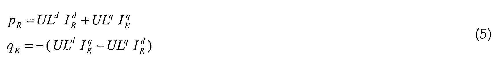
- The current reference values I d / R and I q / R may be limited in accordance with specified operating conditions for the transmission system before further processing but such limitation means, which may be implemented in per se known ways, are not treated in this context.
- It is noted that in a dq -reference plane rotating in synchronism with the bus voltage as described above, the q -component of the bus voltage becomes zero. It then follows from expression (5) that the d -component of the current reference value becomes a reference value for active power and the q - component a reference value for reactive power.
- The actual value I of the alternating current is sensed in the alternating current network at the converter and transformed to the dq -reference plane as an actual current vector
I dq (the transformation not shown in the figure). - Current controller 42 is supplied with the current reference vector
I dq / R, the actual current vectorI dp , and with a mean valueUL dq / m of the bus voltage UL transformed to the dq -reference plane. The current controller outputs in dependence thereon an output signal designatedU V dq / R, which is the alternating voltage reference vector for the bridge voltage of the converter in the dq - reference plane. For a detailed description of an embodiment of the internal structure of the current controller, reference is made to Anders Lindberg, in particular pages 1, and 77-106. - The alternating voltage reference vector
U V dq / R is supplied to a transformation member 43, transforming the vector to the αβ -reference plane. The output of the transformation member 43 is supplied to a transformation member 44, transforming the supplied vector to the abc-reference plane as a vectorU V abc / R. This vector is the bridge voltage reference vector for the converter, having as components the voltage reference templates, i.e. voltage reference values, for the respective three phases of the alternating current system. - The voltage reference vector
U V abc / R is supplied to pulse width modulation unit 23 as described above with reference to figure 2. - The transformation member 43 performs in a way known per se the transformation
U V αβ / R =U V dq / R * e jζ , which follows from the expressions (2) - (4) with ϕ=0 and the transformation angle ζ = ωt. - A transformation angle signal, in the figure designated ζ, is in a conventional manner generated by the phase-locked loop (PLL) member 46, in dependence on the nominal value ƒ0 of the frequency of the alternating current electric power network, and of the phase position of the bus voltage UL, transformed to the αβ -reference plane, and then supplied to the transformation member 43.
- The signal ξ can be conceived of as a phase reference synchronising signal, in the following shortly referred to as synchronising signal or phase angle signal. It has the purpose of synchronising the rotating dq -reference plane with the bus voltage abc - system, and represents an electrical angle linearly increasing with time with a time rate proportional to the actual frequency of the alternating current network. At least under steady state conditions the synchronising signal ξ is locked to and in phase with the phase position of the bus voltage of the alternating current network. Then, also the rotating dq-reference plane is locked to and maintained in synchronism with the three-phase abc -system and in particular with the bus voltage. Under these conditions, also the q -component of the bus voltage becomes zero.
- In the general case, the converter will transmit an active power, which implies that there is a phase difference δ between the bus voltage and the voltage generated by the converter. Thus, although not particularly shown in figure 3, the voltage reference vector
U V αβ / R will in the general case have a phase position ζ' = ζ + δ , where the transformation angle ζ= ωt. - This is further illustrated in figure 7, in which the phase positions of the voltage reference vector
U V αβ / R and of the bus voltage vectorU L αβ in the αβ -reference plane are shown. In this figure, the horizontal axis, labelled α (Re) and the vertical axis, labelled β (Im) are the orthogonal axis of the αβ -reference plane. As can be readily seen from the figure, with the phase difference δ equal to zero, i.e. with no active power transmitted by the converter, the phase positions of the two voltage vectors coincide. With active power transmitted, the voltage reference vectorU V αβ / R will have a phase position ζ' determined by the relation ξ' = ξ + δ , in which ξ is the phase position of the bus voltage vector ULαβ.
Thus, in the general case, the phase position of the voltage reference vectorU V αβ / R will have a phase position ξ'. - As known in the prior art and indicated by the saw-tooth shapes in figure 2, pulse width modulation unit 23 in principle determines the time instants ta, tb, tc for the commutation of the valves in the respective phase a, b and c of the converter by comparing the amplitudes of the respective components of the voltage reference vector with carrier waves of triangular shape, i.e. a commutation is initialised at each intersection between the respective component of the voltage reference vector and the associated carrier wave.
- A pulse number p is defined as the ratio of the frequency ƒc of the carrier wave and the fundamental frequency ƒ of the voltage reference template.
- Various main circuit configurations of voltage source converters, such as 2-level and 3-level bridges, as well as their principles of operation, are well known in the art, reference is made to for example Anders Lindberg, pages 8-16.
- Depending on the kind of converter bridge, the carrier waves are arranged somewhat differently. Thus, for a 2-level converter, the carrier wave is symmetrical around the zero level and has peak values corresponding to +Ud /2 and -Ud /2, where Ud is the DC voltage of the capacitor equipment to which the converter is coupled. For a 3-level converter, two carrier waves are used for each phase, a positive one oscillating between peak values corresponding to zero and to + Ud / 2, and a negative one oscillating between peak values corresponding to -Ud /2 and zero. The two carrier waves are synchronised in such a way that their most positive peak values coincide in time, intersections between the positive carrier wave and the respective component of the voltage reference vector being used for positive values of the reference voltage, and intersections between the negative carrier wave and the reference voltage being used for negative values of the reference voltage. Reference is made to for example Anders Lindberg, figures 3.9 and 3.10 on pages 36-37.
- According to the state of the art (se for example Anders Lindberg, pages 21-46), with the converter control equipment operating as a sampled control system with a sample period time Ts, the time instants ta, tb, and tc are, as will be described in more detail below, calculated as time delays from a sample instant in dependence on the sample period time and a so-called modulation index.
- In such a case, there is no need to generate an explicit carrier wave for comparison with the voltage reference template.
- However, an implicit underlying carrier wave may still be visualized, having a period time that is twice the sample period time, and with its peak values of the carrier wave, the most positive as well as the most negative ones, coinciding in time with the sample instants. The phase angle of the implicit carrier wave may then be defined such that at the peak values, the phase angle is for a 3-level converter k * π, and for a 2-level converter k *π + π /2, where k is an integer 0, 1,2,....
- In this context, it is noted that the phase angle of the voltage reference templates is defined such that the zero crossings of the templates correspond to phase angles 0° and 180°.
- Thus, under the assumption that the converter control equipment operates as a sampled control system, the sample period time Ts of the time-discrete control system becomes
- The commutation time tx for a phase a, b, c ( x = a, b, or c ), being the time delay between the sample instant and the commutation instant of the respective converter valve, may be calculated as
- The parameter m is the so-called modulation index,
- The first calculating unit 48 (figure 3) is supplied with an input signal representative of a frequency, and comprises a multiplying member 71 and an inverting member 72. The multiplying member is supplied with the frequency value of the input signal and with a predetermined parameter value 2p . The inverting member is supplied with the result of the multiplication and thus outputs a sample period time Ts that is dependent on the inputted frequency value.
- The pulse width modulation unit 23 (see also figure 2) is embodied as a second calculating unit 23 that is supplied with current values of the sample period time as provided by the inverting member 72, with the voltage reference vector
U V abc / R expressed in the abc-reference plane, and with the DC-voltage Ud . - The calculating unit processes in a way known per se the three phase components UV a / R, UV b / R, and UV c / R of the voltage reference vector, and calculates for each phase the respective commutation time according to the relations (7) and (8) above.
- In a way known per se, the switching logic unit 24 is supplied with the calculated commutation times, and generates in dependence thereon via a timer (not shown) that is reset at each sample instant, a train FPa, FPb, and FPc, of turn on/turn off orders supplied to the semiconductor valves.
- Figure 3 illustrates two alternative ways, as known in the prior art, of providing an input signal to the multiplying member 71 of the calculating unit 48.
- In the process of generating the synchronising signal ζ, the phase-locked loop member 46 also generates a value ƒ of the actual frequency of the alternating current network. This value is supplied to the multiplying member 71, and the sample period time Ts of the sampled control system is thus determined as Ts = T l 2 p , wherein T is the period time corresponding to the actual network frequency f .
- Alternatively, as also is indicated in figure 3, the multiplying member 71 is supplied with the nominal value f0 of the frequency of the alternating current electric power network. The sample period time Ts is in this alternative determined as a fixed value Ts = T 0/2p wherein T 0 is the period time corresponding to the nominal frequency ƒ0.
- With the converter coupled to an electric network having an actual fundamental frequency, the nominal value of which is usually 50 or 60 Hz, the converter is controlled to generate an AC voltage having a component of that actual fundamental frequency. However, due to the pulse width modulation system, the generated voltage will also comprise components of other frequencies, typically around the frequency of the carrier wave, as well as subharmonics and low order harmonics of the fundamental frequency.
- Studies have shown that in cases where the sample period time Ts is determined as a fixed value Ts =T 0 /2p, the voltage generated by the converter will contain sub-harmonic components, in a 50 Hz system typically 0.5 Hz, 15 Hz etc.
- Also in cases where the sample period time Ts is determined as a function of the actual network frequency ƒ as described above, the voltage generated by the converter will contain low order harmonic components, such as of the 5th, 7th and the 9th order etc.
- There is a general wish to reduce the switching frequency of the converter in order to reduce the switching losses. However, with a lower switching frequency, the amplitude of the generated frequency components other than of the actual fundamental frequency will increase. This will put heavier demands on the filter circuits in order to meet requirements from customers as well as standardised requirements on harmonic content of the voltage, resulting in greater costs and more space required for the filter circuits.
- It is an object of the present invention to provide a time-discrete pulse-width modulation control equipment for a voltage source converter, in particular a 3-level or a 2-level converter, and a method for controlling such a converter, that reduce the content of sub-harmonic components and in particular reduce the content of low order harmonic components in the voltage generated by the converter.
- From the above description of the prior art, it is observed that in the case when the sample period time Ts is determined as a function of the actual network frequency ƒ, there is a synchronisation in frequency between the actual network frequency and the sample period time, as expressed by the relation (6) above, equivalent to a corresponding synchronisation in frequency between the actual network frequency and an implicit carrier wave (or an explicit carrier wave in control equipment where such a carrier wave is generated).
- However, there is in this prior art no synchronisation with respect to phase, i.e. by using the concept of a carrier wave for visualisation, the phase difference between a respective voltage reference template and the corresponding carrier wave is accidental. This also implies that the distance in time between the sampling instants and the phase positions 0° and 180° of the voltage reference template, i.e. the zero crossings of the voltage reference template, is accidental.
- Obviously, when the sample period time is determined as a fixed value Ts = T 0 /2p, there is no such synchronisation, neither with respect to frequency nor with respect to phase.
- The above mentioned object is according to the invention achieved by providing phase-locking means for synchronising the sample instants and the reference voltage template so that for a 3-level converter the phase positions 0° and 180° of the voltage reference template each coincide with a sample instant, and for a 2-level converter the phase positions 0° and 180° of the voltage reference template each coincide with an instant in time corresponding to a sample instant that is displaced in time with half the sample period time, said phase-locking means for generating, in dependence on the voltage reference template and on a sample period time, a frequency tracking signal tracking the reference frequency of the voltage reference template.
- In an advantageous development of the invention, said phase-locking means comprises a first signal generating means for generation, in dependence on the frequency tracking signal and the sample period time, of a track angle signal for tracking the phase angle value of the voltage reference template, a phase detecting means for generating a phase difference signal in dependence on said track angle signal and the voltage reference template, representative of a phase difference between the reference phase angle of the voltage reference template and said track angle, controller means for generation of a frequency correction signal in dependence on said phase difference signal, and means for generating said frequency tracking signal in dependence on said frequency correction signal.
- In another advantageous development of the invention, said phase detecting means comprises means for forming said phase difference signal via multiplications of components of the voltage reference template by sine and cosines functions of the track angle signal.
- Further advantageous developments of the invention will become clear from the description of preferred embodiments of the invention and the attached claims.
- The invention also relates to a computer program product, and to a computer readable medium according to the attached corresponding patent claims.
- Studies have shown that with control equipment according to the invention, the result will be a substantial reduction of the generated low order harmonics, typically up to 10 times as compared with prior art, as well as of subharmonics.
- The invention will be explained in greater detail by description of preferred embodiments with reference to the accompanying drawings, which are all schematic and in the form of single line diagrams and block diagrams respectively, and wherein
- figure 1
- shows in the form of a schematic single line and block diagram a high voltage direct current transmission system as known in the prior art,
- figure 2
- shows a known embodiment of control equipment for a voltage source converter for a transmission system according to figure 1,
- figure 3
- shows in more detail parts of the control equipment according to figure 2,
- figure 4A
- shows an embodiment of converter control equipment according to the invention, for a 3-level converter,
- figure 4B
- shows parts of an embodiment of converter control equipment according to the invention, for a 2-level converter,
- figure 5
- shows an embodiment of a phase-locking means of converter control equipment according to figures 4A and 4B,
- figure 6
- shows details of a phase-locking means according to figure 5, and
- figure 7
- shows the phase relations between a voltage reference vector and a bus voltage vector in an embodiment of control equipment according to figure 3.
- Figure 4A shows an embodiment of converter control equipment according to the invention, in particular adapted for a 3-level converter. As compared with the known embodiment of such an equipment as described with reference to figure 3, a second phase-locked loop member 47 has been added. As will be explained in further detail below, the member 47 generates and supplies to the multiplying member 71 of the first calculating unit 48 a frequency tracking signal ƒs, that is tracking the reference frequency ƒof the voltage reference template, and is representative of the frequency of the voltage reference vector
U V αβ / R. - This frequency tracking signal ƒs is supplied to the multiplying member 71 instead of, as described above as prior art, a signal representative of the actual frequency value ƒof the alternating current electric power network provided by the phase locked loop member 46 (figure 3), or alternatively, the nominal value ƒ0 of the frequency of the alternating current electric power network.
- Thus, according to the invention, the sample period time Ts is determined as
- In this embodiment of the invention, the phase-locked loop member 47 is supplied with the value of the alternating voltage reference vector
U V αβ / R expressed in the αβ -reference plane, a running value of the sample period time Ts, and the nominal value ƒ0 of the frequency of the alternating current electric power network. - The calculating unit 48 calculates, in the way as described above with reference to figure 3, in dependence on the frequency tracking signal ƒs the sample period time Ts for at least that part of the sampled control system that controls the firing instants of the converter. The respective commutation times for each phase, and the trains FPa, FPb, and FPc, of turn on/turn off orders for the semiconductor valves, are then determined in the way as described above with reference to figure 3.
- Figure 5 shows an embodiment of the phase-locked loop member 47 according to the invention. A phase-angle generating unit 51 generates in dependence on the frequency tracking signal ƒs and the sample period time Ts a track angle signal , that is supplied to a third calculating unit 52. The calculating unit 52 is also supplied with the alternating voltage reference vector
U V αβ / R. As mentioned above, the vectorU V αβ / R has in the general case a phase angle ζ', and the calculating unit 52 calculates in dependence on its inputs an output signal PD, representative of the phase difference ζ' - . The output signal PD is supplied to a controller unit 53, having proportional-integral characteristic. The output of the controller unit is supplied to a filter unit 54 having a low-pass characteristic. The output of the filter unit 54 is designated as a frequency correction signal Δƒ. - The nominal value ƒ0 of the frequency of the alternating current electric power network, and the output Δƒ of the filter unit 54 are supplied to an adding member 56, which outputs the sum thereof as the frequency-tracking signal ƒs. The frequency-tracking signal is supplied to the phase-angle generating unit 51 and to the calculating unit 48.
- Figure 6 shows an embodiment of the phase-angle generating unit 51 and the third calculating unit 52 as described with reference to figure 5. To illustrate the time-discrete function of the sampled control system, the variables ƒs, Ts, and are indicated as ƒs(k), Ts(k), and (k), respectively. The integer k is replacing time as independent variable, and each step in time corresponds to the sample period time Ts .
- A first multiplying member 511 is supplied with the running value ƒs(k) of the frequency-tracking signal and with the factor 2π . The product is supplied to a second multiplying member 512, to which also the current value Ts(k) of the sample period time is supplied. An adding member 513 is supplied with output from the second multiplying member 512 and with the track angle signal value (k-1) as calculated one sample period earlier. The output of the adding member 513, designated '(k), is supplied to one of the inputs of a selector means SW3, the output of which is the current value (k) of the track angle signal .
- The value (k -1) of the track angle signal as calculated one sample period earlier is provided via a delay unit 514, having a transfer function z-1 that indicates a delay with one sample period.
- As is clear from above, the track angle signal is calculated as
- The current value '(k) of the track angle signal is also supplied to a comparator 515, where it is compared with the factor 2π . For the case that '(k) > 2π, the comparator 515 generates a selector signal MD3 that selects a signal having the value '(k) - 2π as the output value (k) for the track angle signal . The signal having the value '(k) - 2π is provided by a difference-forming member 516, which is supplied with and forms the difference of the factor 2π and the output '(k) of the adding member 513.
- Thus, (k) = (k -1) + 2π * ƒs(k) * Ts(k) for (k) ≤ 2π , and (k) = 0 for (k) > 2π, describing a repetitive signal, step-wise increasing from the value zero to the value 2π.
- The third calculating unit 52 comprises a fourth calculating unit 521, supplied with the value (k) of the track angle signal , and which unit, in a way known per se, calculates and outputs the trigonometric functions cos (k) and sin (k).
- The calculating unit 52 further comprises multiplying members 522, 523, and a difference-forming member 524.
- The vector
U V αβ / R has two orthogonal components, designated UV α / R and UV β / R. The component UV α / R can be expressed as UV α / R = - The component UV β / R and the value of the trigonometric function cos (k) are supplied to the multiplying member 522, and the component UV α / R and the value of the trigonometric function sin (k) are supplied to the multiplying member 523.
- The difference-forming member 524 is supplied with the outputs of the members 522 and 523, and forms as output the phase difference signal PD as the difference of the outputs of the multiplying member 522 and the multiplying member 523.
- From the above and from the trigonometric expression for sinus of a difference of two angles, it is clear that the output of the difference-forming member 524 includes a factor sin(ξ' - ) . When the value of approaches the value of ξ', the sine function can with increasing accuracy be replaced by the angle itself, and the phase difference signal PD approaches a value as given by the following expression
- From the feedback and integrating structure of the subsystem made up of the phase-locked loop member 47 and the calculating unit 48 as described with reference to figures 5 and 6, it is clear that this subsystem will tend to settle at a state where the difference (ξ'-) is zero.
- The track angle signal can be interpreted as a signal that tracks the phase position of the voltage reference and which, in steady state, is equal to and representative of the phase position of the voltage reference.
- Also, as described above, the frequency-tracking signal ƒs is determined as ƒs = Δƒ + f0, which implies that at least in steady state, the frequency-tracking signal fs represents a frequency that is equal to and representative of the frequency of the components of the voltage reference vector
U V αβ / R, i.e. of the voltage reference templates. - As described above, the sample period time value Ts outputted from the calculating unit 48 will be Ts = 1/( 2p * ƒs), and the condition that in steady state the difference (ξ'- ) is zero implies that sample instants k * Ts will coincide in time with zero crossings of the voltage reference templates, i.e. where the phase positions of the voltage reference templates are 0° and 180°.
- Further, with the pulse number predetermined to be an even number 2p , there will be exactly 2p sample instants during a full period of the voltage reference. Thus, as is understood from the above description, each sample instant will take place at time instants corresponding to angles
- By putting k = m * p , where m is a natural number 1, 2, 3..., the relation (12) will read
- As mentioned above, due to the feedback and integrating structure of the subsystem made up of the phase-locked loop member 47 and the calculating unit 48, this subsystem will tend to settle at a state where the difference (ζ'-) is zero, which together with the relation (12a) implies that there will be a sample instant occurring exactly at the phase positions 0° and 180° of the voltage reference templates.
- In particular, as there is a whole number of samples over half a period of the voltage reference, one sample, i.e. for k = p, will occur at the angle (k) =π. Thus, with the condition (ζ'-) being zero, also the voltage reference templates will at this sample instant have the phase angle ζ'(k)=π .
- Thus, according to the described invention, the sample instants are synchronised to the reference voltage not only with respect to frequency but also with respect to phase angle in such a way that for a 3-level converter the phase positions 0° and 180° of the voltage reference template each coincide with a sample instant. This is equivalent to that the phase difference between the voltage reference templates and their corresponding carrier waves, implicit or explicit, is 0° or 180°.
- The above-described embodiment of the invention in particular refers to a 3-level converter bridge. However, the invention is also applicable to for example a 2-level converter. The description of the phase locking means and in particular the expressions (9) - (12) above are still valid, assuming that the phase position of the voltage reference template in the αβ -reference plane, when inputted to the phase-locked loop member 47, is displaced an angle that in time corresponds to half of the sample period time. Then, the sample instants will for the 2-level converter be synchronised to the voltage reference templates not only with respect to frequency but also with respect to phase angle, however, in such a way that the phase positions 0° and 180° of the voltage reference templates each coincide with an instant in time corresponding to a sample instant that is displaced in time with half the sample period time (Ts).
- This is equivalent to that the phase difference between the voltage reference templates and their corresponding carrier waves, implicit or explicit, is 0° or 180°.
- This embodiment of the invention is illustrated in figure 4B, showing parts of the converter control equipment as described with reference to figure 4A. The voltage reference vector
U V dq / R is supplied to a transformation member 461, transforming the vector to the αβ -reference plane in dependence on a synchronising signal ζ". The signal ζ" is formed in a summing member 462 as the sum of the synchronising signal ζ, formed by the member 46, and of a phase shift Δζ . The sample period time Ts and the frequency-tracking signal fs are supplied to a multiplying member 463. The output of the multiplying member 463 is supplied to a multiplying member 464, where it is multiplied by the factor π to form the phase shift Δξ as Δξ = 2π *ƒs * Ts /2 . The output of the transformation member 461, labelledU V αβ / RΔ, which thus has the phase displacement Δζ with respect to the voltage reference vectorU V αβ / R as supplied to the transformation member 44, is supplied to the phase-locked loop member 47. - Using the concept of a carrier wave for a visualisation of the invention, the carrier wave signal will, according to the invention, not only have a frequency equal to p times the frequency of the voltage reference templates but also be locked in phase to the phase position of the voltage reference templates in the following way.
- For a 3-level converter, the phase difference between the voltage reference templates and their corresponding carrier waves will in the steady state be equal to m * π where m is a natural number 1, 2, 3..., implying that that there is a synchronisation with respect to frequency as well as with respect to phase position between the carrier wave and the voltage reference template. The phase positions 0° and 180° of the voltage reference template will then each coincide with a sample instant.
- Also for a 2-level converter, the phase difference between the voltage reference templates and their corresponding carrier waves will in the steady state be equal to m * π, implying that there is a synchronisation with respect to frequency as well as with respect to phase position between the carrier wave and the voltage reference template. However, in this case the phase positions 0° and 180° of the voltage reference template will each coincide with an instant in time corresponding to a sample instant that is displaced in time with half the sample period time, i.e. they coincide with an instant in time that is at the positioned midway between two sample instants.
- The invention is not limited to the preferred embodiments described above but a number of modifications will be apparent to a person with ordinary skill in the art within the scope of the claims.
Claims (11)
- A time-discrete pulse-width modulation control equipment for a voltage source converter, in particular a 3-level or a 2-level converter, the control equipment having means (IREG) for generation of an AC-voltage reference template (UV a / R, UV b / R, UV c / R,
U V abc / R,U V αβ / R) for a voltage (U V ) to be generated by the converter, the voltage reference template having a variable reference frequency ( ƒ ) and a reference phase angle (ζ'), and being sampled at consecutive sample instants ( k *Ts) that are separated in time by a variable sample period time (Ts), the control equipment having first means (48) for determination of the sample period time in dependence on an input signal representative of a frequency, and second means (23) for determination of commutation time instants (ta, tb, tc) of the converter in dependence on sampled values of the voltage reference template, a modulation index (m), and the sample period time, characterised in that the control equipment further comprises phase-locking means (47) for synchronising the sample instants and the reference voltage template so that
for a 3-level converter the phase positions 0° and 180° of the reference voltage template each coincide with a sample instant, and
for a 2-level converter the phase positions 0° and 180° of the reference voltage template each coincide with an instant in time corresponding to a sample instant that is displaced in time with half the sample period time (Ts),
said phase-locking means for generating, in dependence on the voltage reference template and on a sample period time determined by the first means (48), a frequency tracking signal ƒ(s) tracking the reference frequency (ƒ) of the voltage reference template and supplied to the first means. - A control equipment according to claim 1, characterised in that the first means (48) for determination of the sample period time comprises means (71) for forming a product by multiplying the frequency tracking signal by twice a pulse number (p), said pulse number being an integer, and means (72) for inverting said product, and outputting the inverted product as the sample period time.
- A control equipment according to claim 2, characterised in that said phase-locking means comprises a first signal generating means (51) for generation, in dependence on the frequency tracking signal (ƒs) and the sample period time, of a track angle signal () for tracking the phase angle value of the voltage reference template, a phase detecting means (52) for generating a phase difference signal ( PD ) in dependence on said track angle signal and the voltage reference template, representative of a phase difference between the reference phase angle (ζ') of the voltage reference template and said track angle, controller means (53, 54) for generation of a frequency correction signal (Δƒ) in dependence on said phase difference signal, and means (56) for generating said frequency tracking signal (ƒs) in dependence on said frequency correction signal.
- A control equipment according to claim 3, wherein the voltage reference template has the form a vector (
U V αβ / R) in a stationary reference frame characterised in that said phase detecting means comprises means (521 - 524) for forming said phase difference signal via multiplications of components of the voltage reference template by sine and cosine functions of the track angle signal. - A method for controlling a voltage source converter, in particular a 3-level or a 2-level converter, having a time-discrete pulse-width modulation control equipment, the control equipment having means (IREG) for generation of an AC-voltage reference template (UV a / R, UV b / R, UV c / R,
U V abc / R,U V αβ / R) for a voltage (U V ) to be generated by the converter, the voltage reference template having a variable reference frequency (ƒ) and a reference phase angle (ξ'), and being sampled at consecutive sample instants ( k * Ts) that are separated in time by a variable sample period time (Ts), the control equipment having first means (48) for determination of the sample period time in dependence on an input signal representative of a frequency, and second means (23) for determination of commutation time instants (ta, tb, tc) of the converter in dependence on sampled values of the voltage reference template, a modulation index (m), and the sample period time, characterised in that the sample instants and the reference voltage template are synchronised in time so that
for a 3-level converter the phase positions 0° and 180° of the reference voltage template each coincide with a sample instant, and
for a 2-level converter the phase positions 0° and 180° of the reference voltage template each coincide with an instant in time corresponding to a sample instant that is displaced in time with half the sample period time ( Ts ), by
generating, in dependence on the voltage reference template and on a sample period time determined by the first means (48), a frequency tracking signal (ƒs) tracking the reference frequency (ƒ) of the voltage reference template, and
supplying said frequency-tracking signal to the first means. - A method according to claim 5, characterised in that the sample period time is formed as a product by multiplying the frequency tracking signal by twice a pulse number (p), said pulse number being an integer, and inverting said product, and outputting the inverted product as the sample period time.
- A method according to claim 6, characterised in that
a track angle signal () for tracking the phase angle value of the voltage reference template is generated in dependence on the frequency-tracking signal (ƒs) and the sample period time,
a phase difference signal ( PD ) representative of a phase difference between the reference phase angle (ξ') of the voltage reference template and said track angle is generated in dependence on said track angle signal and the voltage reference template,
a frequency correction signal (Δƒ) is generated in dependence on said phase difference signal, and
said frequency tracking signal (ƒs) is generated in dependence on said frequency correction signal. - A method according to claim 7, wherein the voltage reference template has the form a vector (
U V αβ / R) in a stationary reference frame, characterised in that said phase difference signal is formed via multiplications of components of the voltage reference template by sine and cosine functions of the track angle signal. - A computer program product comprising computer program code means for performing control of a voltage source converter according to any of claims 5-8.
- A computer program product according to claim 9, supplied at least to a part over a network such as for example Internet.
- A computer readable medium, having a program recorded thereon for performing control of a voltage source converter according to any of claims 5-8.
Applications Claiming Priority (2)
| Application Number | Priority Date | Filing Date | Title |
|---|---|---|---|
| SE0201693 | 2002-06-05 | ||
| SE0201693A SE523758C2 (en) | 2002-06-05 | 2002-06-05 | Control equipment for PWM-modulated voltage-rigid inverter and method of control thereof |
Publications (3)
| Publication Number | Publication Date |
|---|---|
| EP1369984A2 true EP1369984A2 (en) | 2003-12-10 |
| EP1369984A3 EP1369984A3 (en) | 2017-03-01 |
| EP1369984B1 EP1369984B1 (en) | 2019-04-03 |
Family
ID=20288069
Family Applications (1)
| Application Number | Title | Priority Date | Filing Date |
|---|---|---|---|
| EP03076721.4A Expired - Lifetime EP1369984B1 (en) | 2002-06-05 | 2003-06-03 | Control equipment for a time discrete pulse width modulated voltage source converter, and a method for controlling the same |
Country Status (2)
| Country | Link |
|---|---|
| EP (1) | EP1369984B1 (en) |
| SE (1) | SE523758C2 (en) |
Cited By (5)
| Publication number | Priority date | Publication date | Assignee | Title |
|---|---|---|---|---|
| WO2005124985A1 (en) * | 2004-06-15 | 2005-12-29 | Siemens Aktiengesellschaft | Matrix converter for coupling three-phase voltage networks |
| EP1691463A1 (en) * | 2005-02-09 | 2006-08-16 | Magnetek S.p.A. | Method and device for the control of a three-phase inverter |
| US8083993B2 (en) | 2003-06-20 | 2011-12-27 | Riche Diagnostics Operations, Inc. | System and method for coding information on a biosensor test strip |
| CN102608468A (en) * | 2012-03-27 | 2012-07-25 | 上海市电力公司 | Testing system for detecting characteristics of offshore wind power flexible direct current transmission converter |
| CN102882210A (en) * | 2012-10-08 | 2013-01-16 | 东南大学 | Active power filter (APF) device based on double vehicle stability control (VSC) interactive parallelly-connected harmonic compensation open loop and closed loop combination |
Family Cites Families (2)
| Publication number | Priority date | Publication date | Assignee | Title |
|---|---|---|---|---|
| US5648894A (en) * | 1994-09-30 | 1997-07-15 | General Electric Company | Active filter control |
| DE60043190D1 (en) * | 2000-06-02 | 2009-12-03 | Abb Ab | Control method and system for voltage regulation in a converter system |
-
2002
- 2002-06-05 SE SE0201693A patent/SE523758C2/en not_active IP Right Cessation
-
2003
- 2003-06-03 EP EP03076721.4A patent/EP1369984B1/en not_active Expired - Lifetime
Cited By (8)
| Publication number | Priority date | Publication date | Assignee | Title |
|---|---|---|---|---|
| US8083993B2 (en) | 2003-06-20 | 2011-12-27 | Riche Diagnostics Operations, Inc. | System and method for coding information on a biosensor test strip |
| WO2005124985A1 (en) * | 2004-06-15 | 2005-12-29 | Siemens Aktiengesellschaft | Matrix converter for coupling three-phase voltage networks |
| EP1691463A1 (en) * | 2005-02-09 | 2006-08-16 | Magnetek S.p.A. | Method and device for the control of a three-phase inverter |
| US7760526B2 (en) | 2005-02-09 | 2010-07-20 | Power-One Italy, S.P.A. | Method and device for the control of a three-phase inverter |
| CN102608468A (en) * | 2012-03-27 | 2012-07-25 | 上海市电力公司 | Testing system for detecting characteristics of offshore wind power flexible direct current transmission converter |
| CN102608468B (en) * | 2012-03-27 | 2014-11-26 | 上海市电力公司 | Testing system for detecting characteristics of offshore wind power flexible direct current transmission converter |
| CN102882210A (en) * | 2012-10-08 | 2013-01-16 | 东南大学 | Active power filter (APF) device based on double vehicle stability control (VSC) interactive parallelly-connected harmonic compensation open loop and closed loop combination |
| CN102882210B (en) * | 2012-10-08 | 2014-12-17 | 东南大学 | Active power filter (APF) device based on double vehicle stability control (VSC) interactive parallelly-connected harmonic compensation open loop and closed loop combination |
Also Published As
| Publication number | Publication date |
|---|---|
| EP1369984B1 (en) | 2019-04-03 |
| SE0201693D0 (en) | 2002-06-05 |
| SE0201693L (en) | 2003-12-06 |
| SE523758C2 (en) | 2004-05-18 |
| EP1369984A3 (en) | 2017-03-01 |
Similar Documents
| Publication | Publication Date | Title |
|---|---|---|
| EP2036181B2 (en) | Hvdc system and method to control a voltage source converter in a hvdc system | |
| US6400585B2 (en) | Method and control system for voltage control at a converter station | |
| Kim et al. | New control scheme for AC-DC-AC converter without DC link electrolytic capacitor | |
| Sul et al. | Design and performance of a high-frequency link induction motor drive operating at unity power factor | |
| US6594164B2 (en) | PWM controlled power conversion device | |
| EP1187291A2 (en) | Method and system for connecting and synchronizing supplemental power source to a power grid | |
| EP1269600B1 (en) | Synchronous frame regulation to extract a positive sequence component of a line voltage | |
| CN112165244A (en) | Output current-sharing control method for master-slave parallel inverter | |
| EP0732798B1 (en) | PWM control apparatus and a system using same | |
| EP1333568B1 (en) | Direct conversion programmable power source controller | |
| CN106786562A (en) | The self-excitation activation system and method for a kind of SSSC | |
| EP1369984B1 (en) | Control equipment for a time discrete pulse width modulated voltage source converter, and a method for controlling the same | |
| CN108631624B (en) | Cascaded H-bridge rectifier based on three-dimensional modulation and control method thereof | |
| Matsui et al. | A detecting method for active-reactive-negative-sequence powers and its application | |
| US7388766B2 (en) | Harmonic control and regulation system for harmonic neutralized frequency changer | |
| Williams et al. | Discrete controlled harmonic and reactive power compensator | |
| Bojoi et al. | Improved current control strategy for power conditioners using sinusoidal signal integrators in synchronous reference frame | |
| Rahmati et al. | Direct power control of an VHDC system based on VSCs | |
| RU2368992C1 (en) | Three-phase compensator of reactive power and method of its control | |
| Kanaan et al. | Modelling and comparative evaluation of control techniques applied to a PWM three-phase four-wire shunt active power filter | |
| Davoodnezhad | Hysteresis current regulation of voltage source inverters with constant switching frequency | |
| Abbey et al. | Three-level inverter based STATCOM | |
| KARUNYA et al. | Improvement of Power Quality using Advanced Modulation Strategies for the Cascaded Multilevel Based STATCOM | |
| JPH09182455A (en) | Control circuit of three-level inverter | |
| de Preville et al. | STATCOM CONTROL APPROACHES |
Legal Events
| Date | Code | Title | Description |
|---|---|---|---|
| PUAI | Public reference made under article 153(3) epc to a published international application that has entered the european phase |
Free format text: ORIGINAL CODE: 0009012 |
|
| AK | Designated contracting states |
Kind code of ref document: A2 Designated state(s): AT BE BG CH CY CZ DE DK EE ES FI FR GB GR HU IE IT LI LU MC NL PT RO SE SI SK TR |
|
| AX | Request for extension of the european patent |
Extension state: AL LT LV MK |
|
| PUAL | Search report despatched |
Free format text: ORIGINAL CODE: 0009013 |
|
| AK | Designated contracting states |
Kind code of ref document: A3 Designated state(s): AT BE BG CH CY CZ DE DK EE ES FI FR GB GR HU IE IT LI LU MC NL PT RO SE SI SK TR |
|
| AX | Request for extension of the european patent |
Extension state: AL LT LV MK |
|
| RIC1 | Information provided on ipc code assigned before grant |
Ipc: H02M 7/48 20070101AFI20170120BHEP Ipc: H02M 7/5387 20070101ALI20170120BHEP Ipc: H02M 7/5395 20060101ALI20170120BHEP |
|
| STAA | Information on the status of an ep patent application or granted ep patent |
Free format text: STATUS: REQUEST FOR EXAMINATION WAS MADE |
|
| 17P | Request for examination filed |
Effective date: 20170828 |
|
| AKX | Designation fees paid |
Designated state(s): AT BE BG CH CY CZ DE DK EE ES FI FR GB GR HU IE IT LI LU MC NL PT RO SE SI SK TR |
|
| AXX | Extension fees paid |
Extension state: AL Extension state: MK Extension state: LT Extension state: LV |
|
| RAP1 | Party data changed (applicant data changed or rights of an application transferred) |
Owner name: ABB SCHWEIZ AG |
|
| REG | Reference to a national code |
Ref country code: DE Ref legal event code: R079 Ref document number: 60351908 Country of ref document: DE Free format text: PREVIOUS MAIN CLASS: H02M0007480000 Ipc: H02M0007538700 |
|
| GRAP | Despatch of communication of intention to grant a patent |
Free format text: ORIGINAL CODE: EPIDOSNIGR1 |
|
| STAA | Information on the status of an ep patent application or granted ep patent |
Free format text: STATUS: GRANT OF PATENT IS INTENDED |
|
| RIC1 | Information provided on ipc code assigned before grant |
Ipc: H02M 7/5387 19850101AFI20181107BHEP Ipc: H02M 7/5395 19850101ALI20181107BHEP |
|
| INTG | Intention to grant announced |
Effective date: 20181122 |
|
| RIC1 | Information provided on ipc code assigned before grant |
Ipc: H02M 7/5387 20070101AFI20181107BHEP Ipc: H02M 7/5395 20060101ALI20181107BHEP |
|
| GRAS | Grant fee paid |
Free format text: ORIGINAL CODE: EPIDOSNIGR3 |
|
| GRAA | (expected) grant |
Free format text: ORIGINAL CODE: 0009210 |
|
| STAA | Information on the status of an ep patent application or granted ep patent |
Free format text: STATUS: THE PATENT HAS BEEN GRANTED |
|
| AK | Designated contracting states |
Kind code of ref document: B1 Designated state(s): AT BE BG CH CY CZ DE DK EE ES FI FR GB GR HU IE IT LI LU MC NL PT RO SE SI SK TR |
|
| REG | Reference to a national code |
Ref country code: GB Ref legal event code: FG4D |
|
| REG | Reference to a national code |
Ref country code: CH Ref legal event code: EP Ref country code: AT Ref legal event code: REF Ref document number: 1116986 Country of ref document: AT Kind code of ref document: T Effective date: 20190415 |
|
| REG | Reference to a national code |
Ref country code: DE Ref legal event code: R096 Ref document number: 60351908 Country of ref document: DE |
|
| REG | Reference to a national code |
Ref country code: IE Ref legal event code: FG4D |
|
| REG | Reference to a national code |
Ref country code: NL Ref legal event code: MP Effective date: 20190403 |
|
| REG | Reference to a national code |
Ref country code: AT Ref legal event code: MK05 Ref document number: 1116986 Country of ref document: AT Kind code of ref document: T Effective date: 20190403 |
|
| PG25 | Lapsed in a contracting state [announced via postgrant information from national office to epo] |
Ref country code: NL Free format text: LAPSE BECAUSE OF FAILURE TO SUBMIT A TRANSLATION OF THE DESCRIPTION OR TO PAY THE FEE WITHIN THE PRESCRIBED TIME-LIMIT Effective date: 20190403 |
|
| PG25 | Lapsed in a contracting state [announced via postgrant information from national office to epo] |
Ref country code: FI Free format text: LAPSE BECAUSE OF FAILURE TO SUBMIT A TRANSLATION OF THE DESCRIPTION OR TO PAY THE FEE WITHIN THE PRESCRIBED TIME-LIMIT Effective date: 20190403 Ref country code: SE Free format text: LAPSE BECAUSE OF FAILURE TO SUBMIT A TRANSLATION OF THE DESCRIPTION OR TO PAY THE FEE WITHIN THE PRESCRIBED TIME-LIMIT Effective date: 20190403 Ref country code: PT Free format text: LAPSE BECAUSE OF FAILURE TO SUBMIT A TRANSLATION OF THE DESCRIPTION OR TO PAY THE FEE WITHIN THE PRESCRIBED TIME-LIMIT Effective date: 20190803 Ref country code: CZ Free format text: LAPSE BECAUSE OF FAILURE TO SUBMIT A TRANSLATION OF THE DESCRIPTION OR TO PAY THE FEE WITHIN THE PRESCRIBED TIME-LIMIT Effective date: 20190403 Ref country code: ES Free format text: LAPSE BECAUSE OF FAILURE TO SUBMIT A TRANSLATION OF THE DESCRIPTION OR TO PAY THE FEE WITHIN THE PRESCRIBED TIME-LIMIT Effective date: 20190403 |
|
| PG25 | Lapsed in a contracting state [announced via postgrant information from national office to epo] |
Ref country code: BG Free format text: LAPSE BECAUSE OF FAILURE TO SUBMIT A TRANSLATION OF THE DESCRIPTION OR TO PAY THE FEE WITHIN THE PRESCRIBED TIME-LIMIT Effective date: 20190703 Ref country code: GR Free format text: LAPSE BECAUSE OF FAILURE TO SUBMIT A TRANSLATION OF THE DESCRIPTION OR TO PAY THE FEE WITHIN THE PRESCRIBED TIME-LIMIT Effective date: 20190704 |
|
| PG25 | Lapsed in a contracting state [announced via postgrant information from national office to epo] |
Ref country code: AT Free format text: LAPSE BECAUSE OF FAILURE TO SUBMIT A TRANSLATION OF THE DESCRIPTION OR TO PAY THE FEE WITHIN THE PRESCRIBED TIME-LIMIT Effective date: 20190403 |
|
| REG | Reference to a national code |
Ref country code: DE Ref legal event code: R097 Ref document number: 60351908 Country of ref document: DE |
|
| PG25 | Lapsed in a contracting state [announced via postgrant information from national office to epo] |
Ref country code: DK Free format text: LAPSE BECAUSE OF FAILURE TO SUBMIT A TRANSLATION OF THE DESCRIPTION OR TO PAY THE FEE WITHIN THE PRESCRIBED TIME-LIMIT Effective date: 20190403 Ref country code: RO Free format text: LAPSE BECAUSE OF FAILURE TO SUBMIT A TRANSLATION OF THE DESCRIPTION OR TO PAY THE FEE WITHIN THE PRESCRIBED TIME-LIMIT Effective date: 20190403 Ref country code: EE Free format text: LAPSE BECAUSE OF FAILURE TO SUBMIT A TRANSLATION OF THE DESCRIPTION OR TO PAY THE FEE WITHIN THE PRESCRIBED TIME-LIMIT Effective date: 20190403 Ref country code: MC Free format text: LAPSE BECAUSE OF FAILURE TO SUBMIT A TRANSLATION OF THE DESCRIPTION OR TO PAY THE FEE WITHIN THE PRESCRIBED TIME-LIMIT Effective date: 20190403 Ref country code: SK Free format text: LAPSE BECAUSE OF FAILURE TO SUBMIT A TRANSLATION OF THE DESCRIPTION OR TO PAY THE FEE WITHIN THE PRESCRIBED TIME-LIMIT Effective date: 20190403 |
|
| REG | Reference to a national code |
Ref country code: CH Ref legal event code: PL |
|
| PLBE | No opposition filed within time limit |
Free format text: ORIGINAL CODE: 0009261 |
|
| STAA | Information on the status of an ep patent application or granted ep patent |
Free format text: STATUS: NO OPPOSITION FILED WITHIN TIME LIMIT |
|
| PG25 | Lapsed in a contracting state [announced via postgrant information from national office to epo] |
Ref country code: IT Free format text: LAPSE BECAUSE OF FAILURE TO SUBMIT A TRANSLATION OF THE DESCRIPTION OR TO PAY THE FEE WITHIN THE PRESCRIBED TIME-LIMIT Effective date: 20190403 |
|
| 26N | No opposition filed |
Effective date: 20200106 |
|
| REG | Reference to a national code |
Ref country code: BE Ref legal event code: MM Effective date: 20190630 |
|
| PG25 | Lapsed in a contracting state [announced via postgrant information from national office to epo] |
Ref country code: TR Free format text: LAPSE BECAUSE OF FAILURE TO SUBMIT A TRANSLATION OF THE DESCRIPTION OR TO PAY THE FEE WITHIN THE PRESCRIBED TIME-LIMIT Effective date: 20190403 |
|
| PG25 | Lapsed in a contracting state [announced via postgrant information from national office to epo] |
Ref country code: IE Free format text: LAPSE BECAUSE OF NON-PAYMENT OF DUE FEES Effective date: 20190603 |
|
| PG25 | Lapsed in a contracting state [announced via postgrant information from national office to epo] |
Ref country code: SI Free format text: LAPSE BECAUSE OF FAILURE TO SUBMIT A TRANSLATION OF THE DESCRIPTION OR TO PAY THE FEE WITHIN THE PRESCRIBED TIME-LIMIT Effective date: 20190403 Ref country code: LU Free format text: LAPSE BECAUSE OF NON-PAYMENT OF DUE FEES Effective date: 20190603 Ref country code: CH Free format text: LAPSE BECAUSE OF NON-PAYMENT OF DUE FEES Effective date: 20190630 Ref country code: BE Free format text: LAPSE BECAUSE OF NON-PAYMENT OF DUE FEES Effective date: 20190630 Ref country code: LI Free format text: LAPSE BECAUSE OF NON-PAYMENT OF DUE FEES Effective date: 20190630 |
|
| PGFP | Annual fee paid to national office [announced via postgrant information from national office to epo] |
Ref country code: DE Payment date: 20200618 Year of fee payment: 18 Ref country code: FR Payment date: 20200619 Year of fee payment: 18 |
|
| PGFP | Annual fee paid to national office [announced via postgrant information from national office to epo] |
Ref country code: GB Payment date: 20200625 Year of fee payment: 18 |
|
| PG25 | Lapsed in a contracting state [announced via postgrant information from national office to epo] |
Ref country code: CY Free format text: LAPSE BECAUSE OF FAILURE TO SUBMIT A TRANSLATION OF THE DESCRIPTION OR TO PAY THE FEE WITHIN THE PRESCRIBED TIME-LIMIT Effective date: 20190403 |
|
| PG25 | Lapsed in a contracting state [announced via postgrant information from national office to epo] |
Ref country code: HU Free format text: LAPSE BECAUSE OF FAILURE TO SUBMIT A TRANSLATION OF THE DESCRIPTION OR TO PAY THE FEE WITHIN THE PRESCRIBED TIME-LIMIT; INVALID AB INITIO Effective date: 20030603 |
|
| REG | Reference to a national code |
Ref country code: DE Ref legal event code: R119 Ref document number: 60351908 Country of ref document: DE |
|
| GBPC | Gb: european patent ceased through non-payment of renewal fee |
Effective date: 20210603 |
|
| PG25 | Lapsed in a contracting state [announced via postgrant information from national office to epo] |
Ref country code: GB Free format text: LAPSE BECAUSE OF NON-PAYMENT OF DUE FEES Effective date: 20210603 Ref country code: DE Free format text: LAPSE BECAUSE OF NON-PAYMENT OF DUE FEES Effective date: 20220101 |
|
| PG25 | Lapsed in a contracting state [announced via postgrant information from national office to epo] |
Ref country code: FR Free format text: LAPSE BECAUSE OF NON-PAYMENT OF DUE FEES Effective date: 20210630 |