EP1363389A2 - Control of an inverter - Google Patents
Control of an inverter Download PDFInfo
- Publication number
- EP1363389A2 EP1363389A2 EP03076276A EP03076276A EP1363389A2 EP 1363389 A2 EP1363389 A2 EP 1363389A2 EP 03076276 A EP03076276 A EP 03076276A EP 03076276 A EP03076276 A EP 03076276A EP 1363389 A2 EP1363389 A2 EP 1363389A2
- Authority
- EP
- European Patent Office
- Prior art keywords
- control section
- control unit
- voltage
- inverter
- circuit
- Prior art date
- Legal status (The legal status is an assumption and is not a legal conclusion. Google has not performed a legal analysis and makes no representation as to the accuracy of the status listed.)
- Withdrawn
Links
Images
Classifications
-
- H—ELECTRICITY
- H02—GENERATION; CONVERSION OR DISTRIBUTION OF ELECTRIC POWER
- H02M—APPARATUS FOR CONVERSION BETWEEN AC AND AC, BETWEEN AC AND DC, OR BETWEEN DC AND DC, AND FOR USE WITH MAINS OR SIMILAR POWER SUPPLY SYSTEMS; CONVERSION OF DC OR AC INPUT POWER INTO SURGE OUTPUT POWER; CONTROL OR REGULATION THEREOF
- H02M7/00—Conversion of ac power input into dc power output; Conversion of dc power input into ac power output
- H02M7/42—Conversion of dc power input into ac power output without possibility of reversal
- H02M7/44—Conversion of dc power input into ac power output without possibility of reversal by static converters
- H02M7/48—Conversion of dc power input into ac power output without possibility of reversal by static converters using discharge tubes with control electrode or semiconductor devices with control electrode
- H02M7/53—Conversion of dc power input into ac power output without possibility of reversal by static converters using discharge tubes with control electrode or semiconductor devices with control electrode using devices of a triode or transistor type requiring continuous application of a control signal
- H02M7/537—Conversion of dc power input into ac power output without possibility of reversal by static converters using discharge tubes with control electrode or semiconductor devices with control electrode using devices of a triode or transistor type requiring continuous application of a control signal using semiconductor devices only, e.g. single switched pulse inverters
- H02M7/5387—Conversion of dc power input into ac power output without possibility of reversal by static converters using discharge tubes with control electrode or semiconductor devices with control electrode using devices of a triode or transistor type requiring continuous application of a control signal using semiconductor devices only, e.g. single switched pulse inverters in a bridge configuration
- H02M7/53871—Conversion of dc power input into ac power output without possibility of reversal by static converters using discharge tubes with control electrode or semiconductor devices with control electrode using devices of a triode or transistor type requiring continuous application of a control signal using semiconductor devices only, e.g. single switched pulse inverters in a bridge configuration with automatic control of output voltage or current
- H02M7/53873—Conversion of dc power input into ac power output without possibility of reversal by static converters using discharge tubes with control electrode or semiconductor devices with control electrode using devices of a triode or transistor type requiring continuous application of a control signal using semiconductor devices only, e.g. single switched pulse inverters in a bridge configuration with automatic control of output voltage or current with digital control
Landscapes
- Engineering & Computer Science (AREA)
- Power Engineering (AREA)
- Inverter Devices (AREA)
- Control Of Ac Motors In General (AREA)
Abstract
Description
- The present invention relates to a control unit for controlling an inverter having a bridge circuit provided with controllable semiconductor switches, which bridge circuit converts a direct voltage fed to the inverter into an alternating voltage of variable frequency and amplitude, said control unit controlling the semiconductor switches by pulse-width modulation (PWM) to produce an output voltage of the inverter.
- The invention relates especially to a PWM inverter control arrangement which comprises a control circuit at ground potential used e.g. for a customer interface and a control circuit at main circuit potential, containing e.g. measuring circuits and circuits producing control signals for power semiconductor switches.
- Such an inverter is applicable for use e.g. in a frequency converter in which the alternating voltage of a three-phase supply network is rectified by a rectifier circuit to produce an intermediate circuit direct voltage and then inverted by means of an inverter to produce a three-phase alternating voltage of variable frequency and amplitude for feeding e.g. a three-phase cage induction motor.
- PWM frequency converters are generally used to control the rotational speed of a cage induction motor, which is the commonest motor type in industry. An output voltage of variable amplitude and frequency is generated by means of the power semiconductor switches of an inverter. For the control of the power semiconductor switches, pulse amplifier circuits at main circuit potential, i.e. at the potential of the power semiconductor switches are needed. To produce a correct output voltage, it is necessary to use measuring circuits, which are normally also at main circuit potential.
- The control circuit processing the signals pertaining to the customer interface again has to be at ground potential for reasons of safety. Therefore, galvanic isolation is required between the control circuit unit at ground potential and the control circuits at main circuit potential.
- A common practice for providing galvanic isolation between the units is to use serial communication via optoisolators or optical fibers. Such an arrangement is known e.g. from patent specification EP0469872, which discloses a system for the control of an adjustable-frequency AC inverter using two serial data channels: one channel for transmitting reference values to a control circuit at main circuit potential and a second channel for transmitting measurement and other feedback data to a control circuit at ground potential.
- The pulse pattern of the voltage produced by the inverter is normally computed either by a microprocessor or an ASIC circuit designed for this purpose. The generation of the pulse pattern is normally based on a predetermined algorithm, e.g. a sine-triangle comparison. The modern efficient microprocessors allow both the functions required for the control of the customer interface and the functions needed for controlling the main circuit to be performed by the same processor, which is normally placed in a the control unit section at ground potential.
- The generation of a pulse pattern implemented in the aforesaid manner involves the problem that the pulse pattern actually produced in the output voltage is not exactly of the desired form. Deviations arise e.g. from signal processing delays in the pulse amplifiers, switching delays in the power semiconductor switches and the required so-called dead time between the conduction periods of the upper and lower arms of the phase switch. Further errors result from a fast variation of the d.c. intermediate circuit voltage. Especially at low frequencies, at which a large number of switching actions occur during a single cycle of the output voltage, the errors clearly distort the output voltage.
- The voltage error can be compensated by measuring the output voltage produced and taking the error into account in connection with the next switching instant. Especially if the pulse pattern is generated at ground potential, the large voltage difference requires the use of difficult and expensive measuring circuits which reduce the ground impedance of the device and may cause problems in the earth-leakage monitoring circuits of the supply network.
- The object of the present invention is to achieve a control system for the control of a PWM-controlled inverter that is better than prior-art solutions, in which system the output voltage is always correct regardless of frequency, power-stage dead time or variations of the intermediate circuit voltage, wherein the phase switches do not have to perform any unnecessary actions, the switching losses being thereby reduced, wherein the angle of the output voltage vector is continuously known, allowing easier motor adjustment especially in difficult applications, and wherein the distribution of tasks between the control unit at ground potential and the control unit at main circuit potential is natural, so that no difficult main circuit measurements are needed and no ground impedance problems caused by them arise.
- In the control system of the invention, this is achieved by calculating in the control unit section at ground potential the instantaneous value of the voltage vector of the output phases, which value is transmitted in serial format over a galvanically isolated channel to the control unit section at main circuit potential, where the modulation, i.e. determination of the phase switch positions is carried out by forming the time integral of the difference between the reference and actual values of the phase voltages, comparing this difference to a positive limit and a negative limit, and if the time integral exceeds the positive or the negative limit, the phase switch is turned accordingly either to the up position or to the down position.
- In an embodiment of the control system of the invention, the angle and amplitude of the output voltage vector is given in the channel between the galvanically isolated control circuits.
- In a second embodiment of the control system of the invention, the reference values of the instantaneous voltages of at least two phase voltages are given in the channel between the galvanically isolated control circuits.
- The features of the invention are presented in detail in the claims below.
- In the following, the invention will be described in detail by the aid of an example with reference to the attached drawings, wherein
- Fig. 1 represents a PWM frequency converter comprising a rectifier, a direct-voltage intermediate circuit, a control unit and an inverter according to the invention,
- Fig. 2 visualizes the serial data traffic and the generation of phase voltages in the control unit,
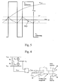
- Fig. 3 visualizes the reading of a sine curve,
- Fig. 4 visualizes the modulation, i.e. determination of the phase switch positions, and
- Fig. 5 represents the voltage reference, error integral, error limits and inverter output voltage pulses.
-
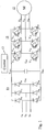
- Fig. 1 represents a prior-art voltage-controlled three-phase PWM frequency converter comprising a
rectifier bridge 10 for the rectification of a three-phase alternating voltage consisting of phase voltages UR, US, UT to produce an intermediate circuit direct voltage UDC and aninverter bridge 11 for DC/AC conversion of the intermediate circuit direct voltage into a three-phase alternating voltage of variable frequency and amplitude having phase voltages UU, UV, UW. The frequency converter feeds a three-phase cage induction motor (M) 12. Theinverter bridge 11 is a full-wave bridge having in the upper and lower arms of the three phases controllable semiconductor switches V11 - V16 with diodes D11 - D16 connected in inverse-parallel with them. Theinverter control unit 13 controls the semiconductor switches V11 - V16 of each phase (V11, V14 in phase U; V12, V15 in phase V, and V13, V16 in phase W) by pulse-width modulation. - Fig. 2 represents the
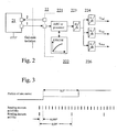
inverter control unit 13, in which theoutward interface part 21 of the control system is grounded and galvanically isolated from thecontrol functions 22 immediately relating to the main circuit by means of two optically isolatedserial data channels control unit section 21 also takes care of actions relating to the adjustment of the output voltage, such as the computations relating to motor adjustment, actions associated with supply network failures, etc., and sends the values of the output voltage vector obtained as a final result to thecontrol circuits 22 of the main circuit. -
Control unit section 22 performs the modulation, i.e. the determination of the phase switch positions, main circuit measurements and actions relating to immediate protection of the power stage. - Of the two optically isolated channels between the control unit and the main circuit,
channel 1 is used for transmitting reference values by giving the angle and amplitude of the output voltage vector during operation, instead of which it is also possible give the instantaneous values of the phase voltages. The reference values are given precisely at predetermined intervals, e.g. at every 50µs. The direction of rotation of the vector angle also determines the direction of rotation of the motor. In addition to the transmission ofreference values channel 1 can also be used for other actions, such as carrying out inquiries concerning the power stage in connection with start-up and giving a switching frequency reference and start/stop data. -
Channel 2 is used for the transmission of feedback signals: motor currents, DC voltage, temperatures and malfunction and warning notices during operation and for responding to inquiries relating to the power stage in connection with start-up. - When
channel 1 transmits the angle and amplitude of the output voltage vector, the unscaled instantaneous values of the phase voltages are read from memory on the basis of an angle reference and multiplied by an amplitude reference. If the sinusoidal phase voltage reference curve is combined with the 3rd harmonic, which is a well-known expedient used to achieve a larger output voltage, then the quarter period (90°) values of the sine curve have to be programmed in memory. If the sine curve is not combined with the 3rd harmonic, only the 60° values have to be stored in memory. - The table below and Fig. 3 present an example of reading the sine curve if the curve has been saved at 0.1° intervals and it is read at 50µs intervals, using a few different initial frequency values f. In the table, T is the output voltage cycle time calculated from the formula T=1/f, and α is the angle corresponding to a 50µs period in the output voltage, calculated from the formula α = 50µs/T*360°:
f [Hz] T [ms] α [°] 0.5 2000 0.009 5 200 0.09 50 20 0.9 500 2 9 - The readings obtained from the
memory 222 are multiplied in amicrocircuit 221 by the amplitude reference and D/A-converted in aconverter 223 to produce inreference value units - The modulation, i.e. determination of the positions of the phase switches V11 - V16 is performed by coupling as presented in Fig. 4 as follows e.g. for phase U:
- 1. The actual value UUact of the phase voltage is formed by measuring the voltage between the output voltage UU produced by the inverter and the midpoint of the intermediate circuit voltage UDC (between resistors R1 and R2).
- 2. In an
integrator 31 composed of amplifier circuits, the time integral El of the difference (=voltage error) between the phase voltage reference UUref and the actual value UUact of the phase voltage is formed. It is compared in acomparator - 3. If the error integral El exceeds +- error limit L+, then an upper-arm switch, e.g. V11 is turned on, and similarly when the integral falls below - error limit L, a lower-arm switch, e.g. V14 is turned on (Fig. 5).
- 4. The magnitude of the error limits is determined by a switching frequency reference; the larger the range between the limits, the lower is the switching frequency. A separate controller takes care of the limits in accordance with the switching frequency reference, which is given by the control unit in connection with start-up.
- 5. As is known, simultaneous turning of two phase switches may produce larger than normal overvoltages in the motor, so it is preferable to avoid such a situation. If at the instant at which a given switch should be turned some other switch is being turned or the dead time following switching has not yet elapsed, then the turning of the switch in question is delayed until the relevant time has elapsed. The error integral El does exceed the limit for an instant, but the error is compensated by the next switching instant.
- 6. In certain situations, such as e.g. in the stop state, the error integral has to be reset by a switch connected across an integrating capacitor.
-
- It is obvious to the person skilled in the art that different embodiments of the invention are not limited to the example described above, but that they may be varied within the scope of the claims presented below. The computation relating to the magnitude and frequency of the output voltage can also be carried out e.g. in the
control circuits 22 of the main circuit and the above-described analog generation of error integrals can also be performed digitally e.g. by taking samples of the actual values measured by an A/D converter and executing an integration and a comparison e.g. by means of a microprocessor.
Claims (8)
- Inverter control unit having a bridge circuit provided with controllable semiconductor switches (V11 - V16) in upper and lower circuit arms, which bridge circuit converts a direct voltage (UDC) to be fed to the inverter into an alternating voltage (UU, UV, UW) of variable frequency and amplitude, said control unit controlling the semiconductor switches by pulse-width modulation (PWM) to generate an inverter output voltage, and said control unit comprising a first control section (21) at ground potential and a second control section (22) at the potential of the semiconductor switches, galvanically isolated channels being provided between said sections for serial transmission of control data from the first control section to the second control section and of feedback data from the second control section to the first control section,
characterized in that
a modulation circuit controlling the semiconductor switches (V11 - V16) is disposed in the second control section (22) at the potential of the semiconductor switches, and that
the modulation circuit forms the time integral of the difference between the reference and actual values (Uuref, Uuact) of the phase voltages of the inverter and compares this difference to positive and negative limits (L+, L-) and when the time integral exceeds the positive or the negative limit, drives the phase switch in the upper or lower arm of the phase in question into conduction. - Control unit according to claim 1, characterized in that the second control section (22) contains a circuit for forming the actual values of the phase voltages, which circuit forms the actual values of the phase voltages from between the output voltages of the output phases of the inverter and the midpoint of the intermediate circuit voltage of the frequency converter.
- Control unit according to claim 1, characterized in that the computation circuit associated with the magnitude and frequency of the output voltage is disposed in the first control section (21).
- Control unit according to claim 1, characterized in that, in the channel (1, 2) between the galvanically isolated control unit sections, the angle and amplitude of the output voltage vector are given.
- Control unit according to claim 1, characterized in that the reference values of the instantaneous voltages of at least two phase voltages are given in the channel (1, 2) between the galvanically isolated control circuits.
- Control unit according to any one of claims 1 or 4,
characterized in that, on the basis of an output voltage vector reference it has received, the second control section (22) forms the references for the instantaneous values of two output voltages by reading on the basis of the angle data the voltage values from a memory circuit (222) and multiplying the result by the vector amplitude data, and that the voltage data are converted into analog form by a D/A converter (223), and that the third phase voltage reference is formed by a summing unit (226) from the sum of the aforesaid two references. - Control unit according to any one of claims 1 or 4,
characterized in that, on the basis of an output voltage vector reference it has received, the second control section (22) forms the references for the instantaneous values of each output voltage by reading on the basis of the angle data the voltage values from a memory circuit (222) and multiplying the result by the vector amplitude data, and that the voltage data are converted into analog form by a D/A converter (223). - Control unit according to claim 1, characterized in that the computation circuit associated with the magnitude and frequency of the output voltage is disposed in the second control section (22).
Applications Claiming Priority (2)
| Application Number | Priority Date | Filing Date | Title |
|---|---|---|---|
| FI20020933A FI112558B (en) | 2002-05-17 | 2002-05-17 | Inverter control |
| FI20020933 | 2002-05-17 |
Publications (2)
| Publication Number | Publication Date |
|---|---|
| EP1363389A2 true EP1363389A2 (en) | 2003-11-19 |
| EP1363389A3 EP1363389A3 (en) | 2006-02-22 |
Family
ID=8563959
Family Applications (1)
| Application Number | Title | Priority Date | Filing Date |
|---|---|---|---|
| EP03076276A Withdrawn EP1363389A3 (en) | 2002-05-17 | 2003-05-02 | Control of an inverter |
Country Status (3)
| Country | Link |
|---|---|
| US (1) | US6807074B2 (en) |
| EP (1) | EP1363389A3 (en) |
| FI (1) | FI112558B (en) |
Families Citing this family (11)
| Publication number | Priority date | Publication date | Assignee | Title |
|---|---|---|---|---|
| PL1761984T3 (en) * | 2004-03-16 | 2013-09-30 | Tecogen Inc | Engine driven power inverter system with cogeneration |
| FI121491B (en) * | 2004-11-11 | 2010-11-30 | Vacon Oyj | Overvoltage protection for a drive |
| FI121803B (en) * | 2005-05-03 | 2011-04-15 | Vacon Oyj | Frequency converter monitoring arrangement |
| US7932693B2 (en) * | 2005-07-07 | 2011-04-26 | Eaton Corporation | System and method of controlling power to a non-motor load |
| US7468595B2 (en) * | 2005-07-26 | 2008-12-23 | Eaton Corporation | System and method of controlling the start-up of an adjustable speed motor drive based sinusoidal output power conditioner |
| US7193388B1 (en) | 2006-02-02 | 2007-03-20 | Emerson Electric Co. | Offset PWM signals for multiphase motor |
| US8111012B2 (en) * | 2007-03-05 | 2012-02-07 | Tecey Software Development Kg, Llc | Method and firmware for controlling an inverter voltage by drive signal frequency |
| US10243500B2 (en) | 2015-04-20 | 2019-03-26 | Eaton Intelligent Power Limited | Method to reduce electromagnetic interference in switching circuit applications |
| DE112016007532T5 (en) * | 2016-12-21 | 2019-09-26 | Vacon Oy | PRIORIZED SERIAL COMMUNICATION |
| JP7390881B2 (en) * | 2019-12-11 | 2023-12-04 | 富士フイルムヘルスケア株式会社 | Power conversion equipment, X-ray imaging equipment, motor drive equipment |
| US11936327B2 (en) | 2021-06-23 | 2024-03-19 | Tecogen Inc. | Hybrid power system with electric generator and auxiliary power source |
Citations (3)
| Publication number | Priority date | Publication date | Assignee | Title |
|---|---|---|---|---|
| EP0469872A2 (en) * | 1990-07-31 | 1992-02-05 | Eaton Corporation | Isolated adjustable frequency AC inverter control |
| EP0469873A2 (en) * | 1990-07-31 | 1992-02-05 | Eaton Corporation | Waveform generator for inverter control |
| US5870297A (en) * | 1996-11-25 | 1999-02-09 | Asea Brown Boveri Ag | Device for compensating the DC offset of a converter using a controller |
Family Cites Families (6)
| Publication number | Priority date | Publication date | Assignee | Title |
|---|---|---|---|---|
| GB2186127B (en) * | 1986-01-11 | 1990-03-21 | Hitachi Ltd | Apparatus for controlling power transducers |
| JPS6373898A (en) * | 1986-09-12 | 1988-04-04 | Matsushita Electric Ind Co Ltd | Inverter |
| JPH0469872A (en) | 1990-07-11 | 1992-03-05 | Nec Gumma Ltd | Stepping motor driving circuit for flexible disk device |
| JP3116698B2 (en) | 1993-12-22 | 2000-12-11 | 松下電器産業株式会社 | Inverter voltage detector |
| KR200154582Y1 (en) * | 1996-11-09 | 1999-08-16 | 윤종용 | Driving circuit for inverter of a brushless dc-motor |
| US5990658A (en) * | 1998-01-22 | 1999-11-23 | Allen-Bradley Company, Llc | Apparatus for controlling reflected voltage on motor supply lines |
-
2002
- 2002-05-17 FI FI20020933A patent/FI112558B/en not_active IP Right Cessation
-
2003
- 2003-05-02 EP EP03076276A patent/EP1363389A3/en not_active Withdrawn
- 2003-05-16 US US10/438,826 patent/US6807074B2/en not_active Expired - Fee Related
Patent Citations (3)
| Publication number | Priority date | Publication date | Assignee | Title |
|---|---|---|---|---|
| EP0469872A2 (en) * | 1990-07-31 | 1992-02-05 | Eaton Corporation | Isolated adjustable frequency AC inverter control |
| EP0469873A2 (en) * | 1990-07-31 | 1992-02-05 | Eaton Corporation | Waveform generator for inverter control |
| US5870297A (en) * | 1996-11-25 | 1999-02-09 | Asea Brown Boveri Ag | Device for compensating the DC offset of a converter using a controller |
Also Published As
| Publication number | Publication date |
|---|---|
| FI112558B (en) | 2003-12-15 |
| US6807074B2 (en) | 2004-10-19 |
| EP1363389A3 (en) | 2006-02-22 |
| US20030214827A1 (en) | 2003-11-20 |
| FI20020933A0 (en) | 2002-05-17 |
Similar Documents
| Publication | Publication Date | Title |
|---|---|---|
| US6807074B2 (en) | Control of an inverter | |
| US6771522B2 (en) | Inverter parallel operation system | |
| US6621719B2 (en) | Converter with additional voltage addition or subtraction at the output | |
| US5136494A (en) | Power conversion system with instantaneous real power feedback control | |
| US20060132073A1 (en) | Braking chopper | |
| KR20080075309A (en) | Apparatus for detecting input current of inverter and method thereof | |
| US20070279958A1 (en) | Measurement of the current of a frequency converter | |
| KR20080068254A (en) | Apparatus for detecting input current of inverter and method thereof | |
| US6043999A (en) | Apparatus and method for controlling an elevator power supply | |
| US20050281060A1 (en) | Control of an inverter pulse-width modulator | |
| JP2010142066A (en) | Robot | |
| US20050083035A1 (en) | Measurement of energy by means of a frequency converter | |
| CN113950792B (en) | Power regeneration converter and processing method thereof | |
| US7688603B2 (en) | Arrangement for monitoring a frequency converter | |
| KR20140083004A (en) | Elevator control device | |
| JP3979274B2 (en) | Power converter | |
| EP2963754B1 (en) | Decentralized power supply system | |
| KR100288588B1 (en) | 3-phase pulse width modulated converter | |
| WO2021166335A1 (en) | Converter device and power conversion system | |
| KR100839073B1 (en) | Apparatus and method for detecting input current of inverter circuit | |
| KR930010644B1 (en) | Inverter current control device | |
| JP4667771B2 (en) | Inverter device | |
| CN116114160A (en) | Power conversion control device | |
| JP4349068B2 (en) | Matrix converter system | |
| JPH07264870A (en) | Pwm controlled voltage type inverter |
Legal Events
| Date | Code | Title | Description |
|---|---|---|---|
| PUAI | Public reference made under article 153(3) epc to a published international application that has entered the european phase |
Free format text: ORIGINAL CODE: 0009012 |
|
| AK | Designated contracting states |
Kind code of ref document: A2 Designated state(s): AT BE BG CH CY CZ DE DK EE ES FI FR GB GR HU IE IT LI LU MC NL PT RO SE SI SK TR |
|
| AX | Request for extension of the european patent |
Extension state: AL LT LV MK |
|
| PUAL | Search report despatched |
Free format text: ORIGINAL CODE: 0009013 |
|
| AK | Designated contracting states |
Kind code of ref document: A3 Designated state(s): AT BE BG CH CY CZ DE DK EE ES FI FR GB GR HU IE IT LI LU MC NL PT RO SE SI SK TR |
|
| AX | Request for extension of the european patent |
Extension state: AL LT LV MK |
|
| 17P | Request for examination filed |
Effective date: 20060607 |
|
| AKX | Designation fees paid |
Designated state(s): AT BE BG CH CY CZ DE DK EE ES FI FR GB GR HU IE IT LI LU MC NL PT RO SE SI SK TR |
|
| GRAP | Despatch of communication of intention to grant a patent |
Free format text: ORIGINAL CODE: EPIDOSNIGR1 |
|
| STAA | Information on the status of an ep patent application or granted ep patent |
Free format text: STATUS: THE APPLICATION IS DEEMED TO BE WITHDRAWN |
|
| 18D | Application deemed to be withdrawn |
Effective date: 20090613 |