EP1352518B1 - Commande de sensibilite adptative, a base pixel par pixel, destinee a un systeme de production d'images numerique - Google Patents
Commande de sensibilite adptative, a base pixel par pixel, destinee a un systeme de production d'images numerique Download PDFInfo
- Publication number
- EP1352518B1 EP1352518B1 EP02701929A EP02701929A EP1352518B1 EP 1352518 B1 EP1352518 B1 EP 1352518B1 EP 02701929 A EP02701929 A EP 02701929A EP 02701929 A EP02701929 A EP 02701929A EP 1352518 B1 EP1352518 B1 EP 1352518B1
- Authority
- EP
- European Patent Office
- Prior art keywords
- illumination intensity
- determined
- pixel
- intensity level
- transfer control
- Prior art date
- Legal status (The legal status is an assumption and is not a legal conclusion. Google has not performed a legal analysis and makes no representation as to the accuracy of the status listed.)
- Expired - Lifetime
Links
Images


Classifications
-
- H—ELECTRICITY
- H04—ELECTRIC COMMUNICATION TECHNIQUE
- H04N—PICTORIAL COMMUNICATION, e.g. TELEVISION
- H04N25/00—Circuitry of solid-state image sensors [SSIS]; Control thereof
- H04N25/50—Control of the SSIS exposure
- H04N25/57—Control of the dynamic range
- H04N25/571—Control of the dynamic range involving a non-linear response
- H04N25/575—Control of the dynamic range involving a non-linear response with a response composed of multiple slopes
-
- H—ELECTRICITY
- H04—ELECTRIC COMMUNICATION TECHNIQUE
- H04N—PICTORIAL COMMUNICATION, e.g. TELEVISION
- H04N23/00—Cameras or camera modules comprising electronic image sensors; Control thereof
- H04N23/60—Control of cameras or camera modules
- H04N23/617—Upgrading or updating of programs or applications for camera control
-
- H—ELECTRICITY
- H04—ELECTRIC COMMUNICATION TECHNIQUE
- H04N—PICTORIAL COMMUNICATION, e.g. TELEVISION
- H04N23/00—Cameras or camera modules comprising electronic image sensors; Control thereof
- H04N23/60—Control of cameras or camera modules
- H04N23/65—Control of camera operation in relation to power supply
-
- H—ELECTRICITY
- H04—ELECTRIC COMMUNICATION TECHNIQUE
- H04N—PICTORIAL COMMUNICATION, e.g. TELEVISION
- H04N23/00—Cameras or camera modules comprising electronic image sensors; Control thereof
- H04N23/70—Circuitry for compensating brightness variation in the scene
-
- H—ELECTRICITY
- H04—ELECTRIC COMMUNICATION TECHNIQUE
- H04N—PICTORIAL COMMUNICATION, e.g. TELEVISION
- H04N23/00—Cameras or camera modules comprising electronic image sensors; Control thereof
- H04N23/70—Circuitry for compensating brightness variation in the scene
- H04N23/73—Circuitry for compensating brightness variation in the scene by influencing the exposure time
-
- H—ELECTRICITY
- H04—ELECTRIC COMMUNICATION TECHNIQUE
- H04N—PICTORIAL COMMUNICATION, e.g. TELEVISION
- H04N25/00—Circuitry of solid-state image sensors [SSIS]; Control thereof
- H04N25/50—Control of the SSIS exposure
- H04N25/57—Control of the dynamic range
- H04N25/571—Control of the dynamic range involving a non-linear response
-
- H—ELECTRICITY
- H04—ELECTRIC COMMUNICATION TECHNIQUE
- H04N—PICTORIAL COMMUNICATION, e.g. TELEVISION
- H04N25/00—Circuitry of solid-state image sensors [SSIS]; Control thereof
- H04N25/70—SSIS architectures; Circuits associated therewith
- H04N25/76—Addressed sensors, e.g. MOS or CMOS sensors
-
- H—ELECTRICITY
- H04—ELECTRIC COMMUNICATION TECHNIQUE
- H04N—PICTORIAL COMMUNICATION, e.g. TELEVISION
- H04N2201/00—Indexing scheme relating to scanning, transmission or reproduction of documents or the like, and to details thereof
- H04N2201/32—Circuits or arrangements for control or supervision between transmitter and receiver or between image input and image output device, e.g. between a still-image camera and its memory or between a still-image camera and a printer device
- H04N2201/3201—Display, printing, storage or transmission of additional information, e.g. ID code, date and time or title
- H04N2201/3225—Display, printing, storage or transmission of additional information, e.g. ID code, date and time or title of data relating to an image, a page or a document
- H04N2201/3252—Image capture parameters, e.g. resolution, illumination conditions, orientation of the image capture device
Definitions
- the present invention is directed to controlling sensitivity, on a pixel-by-pixel basis, of a digital imager. More specifically, the present invention is directed to adaptively controlling sensitivity, on a pixel-by-pixel basis, of a digital imager to expand a dynamic range of the digital imager.
- digital imagers are characterized by a linear voltage-to-light response, or transfer function; that is, the digital imager output voltage is approximately linearly related to light incident on the digital imager.
- the output voltage transfer function is linearly proportional to the intensity of the light incident upon the digital imager.
- This linear transfer function can be characterized by a dynamic range.
- the dynamic range is defined as the difference between the highest detectable illumination intensity of a scene to the lowest detectable illumination intensity of the scene. It is well understood that the dynamic range of the transfer function sets the overall dynamic range of the digital imager. If the dynamic range of a scene exceeds the dynamic range of a digital imager, portions of the scene will saturate the digital imager and appear either completely black or completely white. This can be problematic for imaging large dynamic range scenes, such as outdoor scenes.
- a conventional digital imager includes a plurality of photosensitive elements commonly referred to as pixels.
- the physical realization of the pixels is either a plurality of phototransistors or a plurality of photodiodes functioning as light-detecting elements.
- the pixel is first reset with a reset voltage that places an electronic charge across the capacitance associated with the diode.
- Electronic charge produced by, for example, a photodiode when exposed to illumination, causes charge of the diode capacitance to dissipate in proportion to the incident illumination intensity of the scene.
- the change in diode capacitance charge is detected and the photodiode is reset.
- the amount of light detected by the photodiode is computed as the difference between the reset voltage and the voltage corresponding to the final diode capacitance charge.
- the sensitivity of a digital imager can in general be defined by the maximum and minimum light intensities of a scene that can be imaged by the digital imager.
- the light or illumination intensity of a scene captured by a pixel of a digital imager is a value related to an output voltage or amount of charge measured at the pixel, photosensitive element.
- Pixel saturation is realized when a photosensitive element, pixel, becomes depleted of charge such that no amount of additional incident light will change the output voltage, thus pixel saturation acts to limit the maximum light intensity of the scene that can be discretely imaged.
- the saturation of a pixel is an illumination intensity level of 100
- all illumination intensity levels of the scene that are above an illumination intensity level of 100 are represented as an illumination intensity level of 100 in the imaged scene, and thus, these illumination intensity levels of the scene that are above an illumination intensity level of 100 are not discretely imaged or are not discernible because notwithstanding the actual illumination intensity level, above 100, the imaged illumination intensity level is 100.
- pixel noise Another example is pixel noise.
- sources of pixel noise are quantization in the conversion of the analog voltage to a digital code, integrated thermal charge production, and voltage reset variation when a pixel is not sampled using a true correlated double sample.
- Pixel noise sets the minimum detectable illumination intensity. Since the human eye has a logarithmic response to intensity, in digital imaging, it is usually noise in the lower intensities that is of concern.
- Both pixel saturation and pixel noise are inherent properties of a digital imager. So, these properties limit the physical sensitivity of a digital imager such that a scene, having a wide range of light (illumination) intensities, cannot be imaged properly; the higher light (illumination) intensities of the scene are washed out in the imaged scene due to pixel saturation, or the low light (illumination) intensities of the scene become less resolvable due to pixel noise.
- FIG. 1 shows a linear transfer control function wherein an integration time, T int , is near a maximum integration time.
- Integration time, T int is the time that a control signal 10 is not set at a reset level.
- the control signal 10 is initially at a reset level (at the beginning of the frame period, F); however, the control signal 10 changes to another level, in this case a collect level, at a point in time, within the frame period, that is equal to a difference between the frame period, F, and the integration time, T int . (In Figure 1 , the difference is very small.)
- the control signal 10 changes back to the reset level at the end of the frame period, F.
- FIG. 2 shows a linear transfer control function wherein the integration time, T int , is decreased.
- integration time, T int is the time that a control signal 10 is not set at a reset level.
- the control signal 10 is initially at a reset level (at the beginning of the frame period, F); however, the control signal 10 changes to another level, in this case a collect level, at a point in time, within the frame period, that is equal to a difference between the frame period, F, and the integration time, T int . (In Figure 2 , the difference is approximately equal to half the frame period, F.)
- the control signal 10 changes back to the reset level at the end of the frame period, F.
- Figure 2 shows a situation where the control signal 10 is set at a level that causes charge to be transferred or collected from the pixel for a shorter duration of time than shown in Figure 1 .
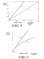
- FIG. 3 Another way of looking at the relationship of the integration time, T int , of the digital imager to the illumination intensity level of the imaged scene is shown in Figure 3 .
- curve A represents a first mapping of pixel output voltage versus illumination intensity level of the imaged scene using a first integration time, T1 int .
- Curve B shows a second mapping of pixel output voltage versus illumination intensity level of the imaged scene using a second integration time, T2 int .
- the second integration time, T2 int is smaller than the first integration time, T1 int .
- the integration time, T int is increased, the slope of the map of pixel output voltage versus illumination intensity level of the imaged scene is increased, thereby emphasizing the lower illumination intensity levels of the imaged scene.
- Another conventional way of manipulating the transfer control function is to use a stepped or piecewise discrete-time transfer control function.
- a stepped or piecewise discrete transfer control function By using a stepped or piecewise discrete transfer control function, the mapping of the pixel output voltage versus illumination intensity level of the imaged scene can be modified to enable a wider range of possible illumination intensity levels of the imaged scene before saturation, while emphasizing low illumination intensity levels of the imaged scene.
- FIG. 4 An example of a conventional stepped or piecewise discrete-time transfer control function is illustrated in Figure 4 .
- the integration time, T int is the same value as illustrated in Figure 1 .
- the level of the control signal 10, in Figure 4 is stepped down in a discrete fashion from a reset level to a collect value.
- the control signal 10 acts as a barrier to charge production or accumulation. At the reset level, a complete barrier is realized wherein no charge is produced or accumulated, notwithstanding the illumination intensity level of the light incident upon the pixel. In other words, the pixel is effectively turned off.
- the control signal 10 is stepped down from a reset level, the effective barrier is lower, thus allowing a rate of production or accumulation of charge to effectively realize a gradual increase.
- the control signal 10 is applied to the pixel or photodiode capacitance to control charge dissipation from the capacitance.
- the control signal 10 is typically decreased from the starting pixel reset voltage value to, e.g., electrical ground or a collect level, with each control signal 10 value at a given time during the exposure period setting the maximum charge dissipation of the photodiode.
- This control signal 10 decrease acts to increase the photodiode charge dissipation capability, whereby the pixel can accommodate a higher illumination intensity before saturating, and the dynamic range of the pixel is thusly increased.
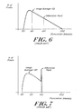
- This charge dissipation control produces a nonlinear pixel output voltage to imaged scene illumination intensity level mapping and a correspondingly expanded dynamic range of the pixel and the imager. This is seen in Figure 5 .
- a mapping of the pixel output voltage versus illumination intensity level of the imaged scene having a wider range is produced.
- curve A shows a mapping of the pixel output voltage versus illumination intensity level of the imaged scene when a linear control transfer function, as illustrated in Figure 1 , is used
- curve B shows a mapping of the pixel output voltage versus illumination intensity level of the imaged scene when a stepped or piecewise discrete-time transfer control function, as illustrated in Figure 4 , is used.
- curve B has a wider range of illumination intensity levels of the imaged scene than curve A.
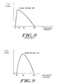
- a histogram of actual illumination intensity levels of a scene to be imaged may include illumination intensity levels from 20 to 200 when the image average is 50; however, due to pixel saturation, illumination intensity levels of the scene above the 100 illumination intensity level will not be represented by the digital imager, as illustrated Figure 7 , because these higher illumination intensity levels of the scene are all bucketed at the 100 illumination intensity level by the digital imager due to pixel saturation, thereby washing out the higher illumination intensity levels of the imaged scene.
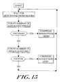
- a histogram of the illumination intensity levels of the imaged scene is realized as illustrated in Figure 8 .
- the histogram of the imaged scene is scaled by a factor of 0.5 such that the image illumination intensity average changes from 50 to 25.
- a greater portion of the higher illumination intensity levels of the scene can be represented; however, the image is unacceptably dark, the quantization noise of the entire image has been cut in half, and the signal may also have been reduced by a factor of 2 while other noise sources stay fixed in magnitude (such as reset noise).
- US 6 040 570 relates to an extended dynamic range imager.
- An array of pixels provides an output signal for each pixel related to an amount of light captured for each pixel during an integration period.
- a row of extended dynamic range (XDR) sample and hold circuits having an XDR sample and hold circuit for each column of the array captures an XDR signal related to a difference between the output signal and an XDR clamp level to which the pixel is reset at a predetermined time before the end of the integration period.
- a row of linear sample and hold circuits having a linear sample and hold circuit for each column of the array captures a linear signal related to a difference between the output signal and an initial output signal to which the pixel is reset at the beginning of the integration period.
- US 6 101 294 concerns an imager that has an array of photodetectors, each of which accumulates charge during an integration period as a result of light detected during said integration period, said array having a charge capacity which increases during the integration period.
- a charge capacity controller coupled to said imager adjusts how the imager increases the charge capacity of the array based upon the brightness distribution detected by said imager during at least one previous integration period.
- DE 197 40 910 describes a method that involves converting a high input dynamic to a reduced output signal dynamic for an image sensor with an arrangement for preventing overcharging. After the scanning of an image, it is determined whether a charge overflow has occurred in at least one image element, and a corresponding overflow signal is produced. An increase of the compression of the signal input dynamic is performed if a corresponding charge overflow occurred, otherwise a reduction of the compression of the input signal dynamic occurs.
- the compression is preferably achieved through thresholds which are adjusted with respect to their temporal duration or their value in response to the overflow signal.
- the present invention concerns a method according to claim 1 and a system according to claim 6.
- a first aspect of the present invention is a method of adaptively controlling sensitivity, on a pixel-by-pixel basis, of a digital imager.
- the method determines a number of pixels of image data having illumination intensity levels within a first defined range of illumination intensity levels; determines an illumination intensity level mapping function based upon the determined number of pixels within the first defined range of illumination intensity levels; determines a transfer control function based on the determined illumination intensity level mapping function; and imposes the determined transfer control function upon a pixel of the digital imager.
- a second aspect of the present invention is a method of adaptively controlling sensitivity, on a pixel-by-pixel basis, of a digital imager.
- the method determines a plurality of numbers of pixels, each determined number of pixels being a number of pixels within an associated defined range of illumination intensity levels; determines a plurality of illumination intensity level mapping functions, each determined illumination intensity level mapping function corresponding to one defined range of illumination intensity levels, each illumination intensity level mapping function being determined based upon the determined number of pixels within the corresponding defined range of illumination intensity levels; determines a transfer control function based on the plurality of determined illumination intensity level mapping functions; and imposes the determined transfer control function upon a pixel of the digital imager.
- a third aspect of the present invention is a method of adaptively controlling sensitivity, on a pixel-by-pixel basis, of a digital imager.
- the method determines a number of saturated pixels; selects a first illumination intensity level mapping function when the determined number of saturated pixels is above a first threshold; determines an number of pixels having illumination intensity levels within a defined range of values; selects a second illumination intensity level mapping function when the determined number of pixels is below a second threshold; determines a transfer control function based on the selected illumination intensity level mapping function; and imposes the determined transfer control function upon a pixel of the digital imager.
- a fourth aspect of the present invention is a method of adaptively controlling sensitivity, on a pixel-by-pixel basis, of a digital imager.
- the method determines a number of pixels of image data having illumination intensity levels within a first defined range of illumination intensity levels, the first defined range of illumination intensity levels including an illumination intensity level corresponding to a pixel saturation value; determines an illumination intensity level mapping function based upon the determined number of pixels within the first defined range of illumination intensity levels; determines a number of pixels having illumination intensity levels within a second defined range of illumination intensity levels, the second defined range of illumination intensity levels including an illumination intensity level corresponding to a minimum illumination intensity level; determines an integration time based upon the determined number of pixels having illumination intensity levels within the second defined range of illumination intensity levels; determines a transfer control function based on the determined illumination intensity level mapping function and the determined integration time; and imposes the determined transfer control function upon a pixel of the digital imager.
- a fifth aspect of the present invention is a method of adaptively controlling sensitivity, on a pixel-by-pixel basis, of a digital imager.
- the method selects a first illumination intensity level mapping function; determines a first transfer control function based on the selected first compression; imposes the determined first transfer control function upon a pixel of the digital imager; determines a histogram of illumination intensity levels of pixels of image data being generated by the digital imager having the determined first transfer control function imposed thereon; determines an illumination intensity level maximum, the illumination intensity level maximum representing a greatest illumination intensity level for a pixel in a sample forming the histogram; determines a second illumination intensity level mapping function, based on the determined intensity level maximum, the second illumination intensity level mapping function preventing the generation of any saturated pixels and providing a dynamic range of image data enabling each level in the histogram to be realized by the digital imager; determines a second transfer control function based on the determined second illumination intensity level mapping function; and imposes the determined second transfer control function upon a
- a sixth aspect of the present invention is a method for determining transition points between a plurality of discrete transfer control functions forming a composite transfer control function.
- the method determines an integration time; determines an illumination intensity level mapping function; determines a composite transfer control function based on the determined integration time and determined illumination intensity level mapping function; and determines a timing of each transition point between a plurality of discrete transfer control functions from the determined integration time and the determined illumination intensity level mapping function.
- a seventh aspect of the present invention is a system for adaptively controlling sensitivity, on a pixel-by-pixel basis, of a digital imager.
- the system includes an illumination intensity level mapping controller to determine a number of pixels of image data having illumination intensity levels within a first defined range of illumination intensity levels and to determine an illumination intensity level mapping function based upon the determined number of pixels within the first defined range of illumination intensity levels and a transfer control function generation circuit to determine a transfer control function based on the determined illumination intensity level mapping function and to impose the determined transfer control function upon a pixel of the digital imager.
- An eighth aspect of the present invention is a system for adaptively controlling sensitivity, on a pixel-by-pixel basis, of a digital imager.
- the system includes an illumination intensity level mapping controller to determine a plurality of number of pixels, each determined number of pixels corresponding to one defined range of illumination intensity levels, and to determine a plurality of illumination intensity level mapping functions, each determined illumination intensity level mapping function corresponding to one defined range of illumination intensity levels, each illumination intensity level mapping function being determined based upon the determined number of pixels within the corresponding defined range of illumination intensity levels and a transfer control function generation circuit to determine a transfer control function based on the plurality of determined illumination intensity level mapping functions and to impose the determined transfer control function upon a pixel of the digital imager.
- a ninth aspect of the present invention is a system for adaptively controlling sensitivity, on a pixel-by-pixel basis, of a digital imager.
- the system includes an illumination intensity level mapping controller to determine a number of saturated pixels and to select a first illumination intensity level mapping function when the determined number of saturated pixels is above a first threshold.
- the illumination intensity level mapping controller determines a number of pixels having illumination intensity levels within a defined range of values and selects a second illumination intensity level mapping function when the determined number of pixels is below a second threshold.
- the system further includes a transfer control function generation circuit to determine a transfer control function based on the selected illumination intensity level mapping function and to impose the determined transfer control function upon a pixel of the digital imager.
- a tenth aspect of the present invention is a system for adaptively controlling sensitivity, on a pixel-by-pixel basis, of a digital imager.
- the system includes an illumination intensity level mapping controller to determine a number of pixels of image data having illumination intensity levels within a first defmed range of illumination intensity levels, the first defined range of illumination intensity levels including an illumination intensity level corresponding to a pixel saturation value, and to determine an illumination intensity level mapping function based upon the determined number of pixels within the first defined range of illumination intensity levels; an exposure controller to determine a number of pixels having illumination intensity levels within a second defined range of illumination intensity levels, the second defined range of illumination intensity levels including an illumination intensity level corresponding to a minimum illumination intensity level, and to determine an integration time based upon the determined number of pixels having illumination intensity levels within the second defined range of illumination intensity levels; and a transfer control function generation circuit to determine a transfer control function based on the determined illumination intensity level mapping function and the determined integration time and to impose the determined transfer control function upon a pixel of the digital imager.
- An eleventh aspect of the present invention is a system for adaptively controlling sensitivity, on a pixel-by-pixel basis, of a digital imager.
- the system includes an illumination intensity level mapping controller to select a first illumination intensity level mapping function and a transfer control function generation circuit to determine a first transfer control function based on the selected first compression and to impose the determined first transfer control function upon a pixel of the digital imager.
- the illumination intensity level mapping controller determines a histogram of illumination intensity levels of pixels of image data being generated by the digital imager having the determined first transfer control function imposed thereon and determines an illumination intensity level maximum, the illumination intensity level maximum representing a greatest illumination intensity level for a pixel in a sample forming the histogram.
- the illumination intensity level mapping controller determines a second illumination intensity level mapping function, based on the determined intensity level maximum, the second illumination intensity level mapping function preventing the generation of any saturated pixels and providing a dynamic range of image data enabling each level in the histogram to be realized by the digital imager.
- the transfer control function generation circuit determines a second transfer control function based on the determined second illumination intensity level mapping function and imposes the determined second transfer control function upon a pixel of the digital imager.
- a twelfth aspect of the present invention is for determining transition points between a plurality of discrete transfer control functions forming a composite transfer control function.
- the system includes an exposure controller to determine an integration time; an illumination intensity level mapping controller to determine an illumination intensity level mapping function; and a transfer control function generation circuit to determine a composite transfer control function based on the determined integration time and determined illumination intensity level mapping function and to determine a timing of each transition point between a plurality of discrete transfer control functions from the determined integration time and the determined illumination intensity level mapping function.
- the present invention provides techniques and systems for adjusting the sensitivity, on a pixel-by-pixel basis, of a digital imager by adjusting the transfer control function (resulting in the production of the control signal) through determining an illumination intensity level mapping function and an integration time characteristic of the digital imager in a manner that enables full use of the entire output intensity level range of the digital imager without saturation of the digital imager.
- a frame period is the time period needed to read all the pixels of a digital imager to produce one frame of an imaged scene.
- Integration time refers to the time period, within an overall frame period, that a digital imager is receiving incident light or illumination from a scene being imaged and producing a collectable charge or voltage in response to incident light or illumination of the scene being imaged.
- Illumination intensity level mapping function refers to the analog to digital conversion relationship between an analog signal received from a pixel of the digital imager and a digital signal representing the illumination intensity received by the pixel.
- Output voltage versus illumination intensity level map is a graphical representation of the illumination intensity level mapping function.
- Transfer control function refers to the controlling of the charge dissipation from the pixel of the digital imager during the integration time period through timing manipulation and control signal voltage level or value manipulation.
- Transfer control function generation refers to either the actual generation of the control signal that controls the charge dissipation from the pixel of the digital imager or a signal that is used to generate the control signal that controls the charge dissipation from the pixel of the digital imager.
- the present invention adjusts the integration time and manipulates the transfer control function (resulting in the production of the control signal) to realize a histogram of the imaged scene, as illustrated in Figure 9 .
- the entire histogram is made to fit within the range of the sensor such that no saturation results while keeping the image average at 50 to ensure the image is bright enough to be visually appealing and thus not reducing the signal to noise ratio in the pixels of lower illumination intensities where the human eye is more sensitive to noise.
- the low illumination intensity levels of the scene are emphasized, and the high illumination intensity levels of the scene are discernable, with no pixels becoming saturated during a given frame period, F.
- the present invention varies the sensitivity of each pixel of a digital imager so that if a scene has a wide dynamic range, the digital imager can produce a non-linear mapping of the output voltages from the digital imager to digital illumination intensity levels or values representing the imaged scene.
- the output voltages representing the higher illumination intensity levels of the scene where the eye is less sensitive to quantization noise, are non-linearly mapped to illumination intensity levels such that the resolution of the higher illumination intensity levels are compressed.
- the output voltages representing the low illumination intensity levels of the scene are amplified to ensure the image is bright enough. The results are imaged scenes with appropriate brightness and no saturation.
- the present invention dynamically adjusts the mapping of the output voltages to imaged scene illumination intensity levels, thereby continually compressing or decompressing the resolution of the high illumination intensity levels of the scene, so as to change or unequally distribute the amount of quantization noise for different levels of light (illumination) intensity. Under a completely linear mapping, all possible illumination intensities of the imaged scene would have the same resolution or amount of quantization noise.
- the present invention selectively decreases or compresses the resolution of higher illumination intensity levels, by non-linearly adjusting the mapping of the output voltage versus illumination intensity level of the imaged scene map, to increase the saturation point.
- the result is that given a scene with a wide dynamic range, the output voltages associated with the low illumination intensity level pixels can be amplified enough to have the desired resolution and the output voltages associated with the high illumination intensity level pixels can be mapped to compress the resolution of the high illumination intensity levels to fit within the range of the analog to digital converter associated with the digital imager and avoid saturation.
- a desirable illumination intensity level mapping is automatically determined and the determined illumination intensity level mapping is converted into a transfer control function (resulting in the production of the control signal) for the digital imager.
- the transfer control function (resulting in the production of the control signal) controls the production or accumulation of charge in the photosensitive element, thus controlling the output voltage of the pixel.
- Figure 10 illustrates one embodiment of the present invention that emphasizes the low illumination intensity levels of the scene, and discerns the high illumination intensity levels of the scene, with no pixels becoming saturated during a given frame period, F.
- a system for adaptively controlling sensitivity, on a pixel-by-pixel basis, of a digital imager includes a digital imager 1, an illumination intensity level mapping controller 3, an exposure controller 5, and a transfer control function generation circuit 7.
- the illumination intensity level mapping controller 3 determines a number of pixels of imaged scene having illumination intensity levels within a first defined range of illumination intensity levels.
- the illumination intensity level mapping controller 3 also determines an illumination intensity level mapping function based upon the determined number of pixels within the first defined range of illumination intensity levels.
- the exposure controller 5 determines a number of pixels of the imaged scene having illumination intensity levels within a second defined range of illumination intensity levels and determines an integration time, T int , based upon the determined number of pixels having illumination intensity levels within a second defined range of illumination intensity levels.
- the transfer control function generation circuit 7 determines a transfer control function based on the determined illumination intensity level mapping function and integration time, T int .
- the transfer control function generation circuit 7 further imposes the determined transfer control function upon a pixel of the digital imager.
- the digital imager 1 receives the transfer control function, and produces a control signal 10 therein in accordance with the received transfer control function.
- the transfer control function generation circuit 7 could also produce the control signal 10 directly and feed it to the digital imager 1, wherein the control signal 10 is produced in accordance with the determined transfer control function based on the determined integration time, T int , and determined illumination intensity level mapping function.
- the first defined range of illumination intensity levels is a range of illumination intensity levels including an illumination intensity level representing pixel saturation
- the second defined range of illumination intensity levels is a range of illumination intensity levels including an illumination intensity level representing a minimum illumination intensity level that may be adjusted for pixel noise or pixel offset.
- the illumination intensity level mapping controller 3 determines a number of pixels of image data having illumination intensity levels within a first defined range of illumination intensity levels from a frame of pixels of image data created by the digital imager, from a partial frame of pixels of image data created by the digital imager, from a defined area within a frame of pixels of image data created by the digital imager, or from a user-defined area within a frame of pixels of image data created by the digital imager.
- the illumination intensity level mapping function can be either calculated or selected from a plurality of pre-specified illumination intensity level mapping functions, preferably from eight pre-specified illumination intensity level mapping functions, based upon the determined number of pixels within the first defined range of illumination intensity levels.
- the transfer control function can be either calculated or selected from a plurality of pre-specified transfer control functions based upon the determined illumination intensity level mapping function and determined integration time, T int .
- the determination of the transfer control function can realized during the generation of a second frame of image data that is immediate subsequent to the frame of image data being used to make the determination.
- the new transfer control function is imposed upon pixels during the generation of a third frame of image data, the third frame being immediate subsequent to the second frame of image data.
- the determination of the transfer control function can realized during the generation of a first frame of image data which is the frame of image data having the partial frame of image.
- the new transfer control function is imposed upon pixels during the generation of a second frame of image data, the second frame being immediate subsequent to the first frame of image data.
- frame period, F, or other frame parameters can be adjusted on the fly to enable implementation of the present invention.
- the illumination intensity level mapping function may be determined independent of, dependent upon, after, before, or substantially simultaneous with the determination of the integration time, T int .
- the illumination intensity level mapping function may be a composite function comprising individual discrete functions wherein each individual discrete illumination intensity level mapping function is determined based upon the determination of a number of pixels within a defined range of illumination intensity levels. Each individual illumination intensity level mapping function is associated with a defined range of illumination intensity levels.
- the illumination intensity level mapping controller 3 determines a plurality of number of pixels, each determined number of pixels corresponding to one defined range of illumination intensity levels. In this embodiment, the illumination intensity level mapping controller 3 determines a plurality of illumination intensity level mapping functions, each determined illumination intensity level mapping function corresponding to one defined range of illumination intensity levels. Each illumination intensity level mapping function is determined based upon the determined number of pixels within the associated defined range of illumination intensity levels.
- the transfer control function generation circuit 7 determines a transfer control function based on the plurality of determined illumination intensity level mapping functions and imposes the determined transfer control function upon a pixel of the digital imager.
- the illumination intensity level mapping controller 3 determines a number of saturated pixels and selects a first illumination intensity level mapping function when the determined number of saturated pixels is above a first threshold.
- the illumination intensity level mapping controller 3 determines a number of pixels having illumination intensity levels within a defined range of levels and selects a second illumination intensity level mapping function when the determined number of pixels is below a second threshold.
- the transfer control function generation circuit 7 determines a transfer control function based on the selected illumination intensity level mapping function and imposes the determined transfer control function upon a pixel of the digital imager.
- the transfer control function may comprise a plurality of discrete transfer control functions, preferably eight discrete transfer control functions.
- the determined illumination intensity level mapping function comprises a plurality of discrete illumination intensity level mapping functions, preferably eight discrete illumination intensity level mapping functions. Each discrete transfer control function is determined based on one of the plurality of distinct illumination intensity level mapping functions.
- Each discrete illumination intensity level mapping function may be a linear illumination intensity level mapping function.
- the plurality of discrete linear illumination intensity level mapping functions form a composite piece-wise linear illumination intensity level mapping function, the composite piece-wise linear compression being the determined illumination intensity level mapping function.
- the determined composite illumination intensity level mapping function is a nearly logarithmic illumination intensity level mapping function.
- the illumination intensity level mapping controller 3 selects a first illumination intensity level mapping function, and the transfer control function generation circuit 7 determines a first transfer control function based on the selected first illumination intensity level mapping function and imposes the determined first transfer control function upon a pixel of the digital imager.
- the illumination intensity level mapping controller 3 determines a histogram of illumination intensity levels of pixels of the imaged scene being generated by the digital imager having the determined first transfer control function imposed thereon and determines an illumination intensity level maximum, the illumination intensity level maximum representing a greatest illumination intensity level for a pixel in a sample forming the histogram.
- the illumination intensity level mapping controller 3 determines a second illumination intensity level mapping function, based on the determined intensity level maximum, the second illumination intensity level mapping function preventing the generation of any saturated pixels and providing a dynamic range of image data enabling each level in the histogram to be realized by the digital imager.
- the transfer control function generation circuit 7 determines a second transfer control function based on the determined second illumination intensity level mapping function and imposes the determined second transfer control function upon a pixel of the digital imager.
- the first illumination intensity level mapping function represents a maximum compression of the resolution of the high illumination intensity levels.
- one way of manipulating the transfer control function is to use a stepped or piecewise discrete-time transfer control function.
- the map of the pixel output voltage versus illumination intensity can be modified to enable a wider range of possible illumination intensity levels before saturation, while emphasizing low illumination intensity levels.
- each stepped transfer control function or control signal level must be determined as well as the timing of the transition points between discrete transfer control functions or discrete control signal levels.
- the transfer control function is a stepped or piecewise discrete-time transfer control function, thereby producing a control signal that is a stepped or piecewise discrete-time control signal.
- the illumination intensity level mapping function, g determines the actual discrete transfer control functions, wherein the actual discrete transfer control functions determine each of the actual discrete control signal levels.
- the illumination intensity level mapping function, g is derived from the desired map of output voltage versus illumination intensity level of the imaged scene illustrated in Figure 14 .
- the desired map of output voltage versus illumination intensity level of the imaged scene is a piece-wise discrete mapping, with each discrete mapping corresponding to a different compression of the resolution of the associated illumination intensity level range.
- each discrete compression of the resolution of the associated illumination intensity level range corresponds to a level, b i , in the transfer control function. As the compression of the resolution of the associated illumination intensity level range is increased, the corresponding level, b i , is decreased.
- the transfer control function is a discrete piece-wise linear function, having eight pieces or steps formed by seven transition points, that produces a nearly logarithmic response.
- FIG. 13 An example of a stepped or piecewise discrete-time transfer control function, according to a preferred embodiment of the present invention, is illustrated in Figure 13 .
- the timing of the transition points, t is set forth on the horizontal axis, and a level, b, corresponding to the transfer control function, which corresponds to an amount of the subsequently produced control signal being stepped down from a reset level, is set forth on the vertical axis.
- the stepped or piecewise discrete-time transfer control function in one embodiment of the present invention is realized by:
- the stepped transfer control function is completely constrained; however, it is still necessary to determine when the transition points between the discrete transfer control functions occur during the overall frame period, T max .
- the levels, b i need not be evenly spaced to find the transition points.
- the equal spacing of b is just an example of creating a transfer control function according to the concepts of the present invention.
- the determination of the timing of the transition points is realized by dedicated hardware due to the repetitive nature of the calculation. Once T 0 is found, one simply does a divide by the same denominator five more times. In the preferred embodiment, T 0 is not calculated by dedicated hardware due to inefficiencies, thus the number of possible g's is limited and a table lookup is used to find T 0 .
- the transition points between the plurality of discrete transfer control functions are determined following the determination of an integration time, T int , and an illumination intensity level mapping function, the illumination intensity level mapping function providing the proper compression of the resolution of the high illumination intensity levels of imaged scene and proper emphasis of the low illumination intensity levels of imaged scene.
- the composite transfer control function has eight discrete transfer control functions and seven transition points.
- the first transition point is equal to a difference between a maximum possible integration time, T max , or frame period, F, and the determined integration time, T int .
- Figure 15 illustrates a process utilized by an illumination intensity mapping controller of a preferred embodiment of the present invention.
- the illumination intensity mapping controller takes the imaged scene from the sensor and counts the number of saturated pixels. If there are too many saturated pixels, the illumination intensity mapping controller increases the amount of compression upon the resolution of the high illumination intensity levels.
- the illumination intensity mapping controller also counts the number of pixels in the upper region (bin) of a histogram of the imaged scene to determine if the imaged scene fills the entire range of the histogram. If there are not enough pixels in the upper region (bin), the illumination intensity mapping controller decreases the amount of compression upon the resolution of the high illumination intensity levels. The illumination intensity mapping controller continues this process until there are no saturated pixels and the histogram is completely used.
- the illumination intensity mapping controller can continuously run without having to drastically change the illumination intensity mapping function to determine how to best set it. If the number of illumination intensity mapping steps is minimized under the constraint of stability, eight illumination intensity mapping steps are sufficient. This allows the illumination intensity mapping function to be set within 16 frames as a maximum.
- Figure 16 illustrates a process utilized by a transfer control function generator circuit of a preferred embodiment of the present invention.
- the transfer control function generator circuit sets the initial level, b, of the transfer control function to b 0 .
- a step value, i is set to a value of 1.
- the timing of the transition point, t i is calculated.
- the transfer control function generator circuit goes into a standby state, sending the last establish level, b, to the digital imager, until the calculated transition point, t i , is realized.
- a new level, b is set equal to b i+1 .
- the step value, i is incremented by 1.
- the present invention contemplates both employing preprogrammed illumination intensity level mapping functions as well as computing custom illumination intensity level mapping functions on the fly during a given frame analysis.
- the use of preprogrammed illumination intensity level mapping functions can be preferred for applications in which computational power is to be minimized.
- Real time computation of illumination intensity level mapping functions can be preferred for applications in which flexibility in sensitivity control is desired.
- a customized illumination intensity level mapping function computed to allocate a large number of output levels to that common intensity level would be optimal for efficiently parceling the output range levels.
- computation of a customized illumination intensity level mapping function can be optimal for allocating a large number of output levels to the intensity range of a particular physical region of pixels of an image frame. Such a region may be of interest for its inclusion of, e.g., moving objects, or in general, objects of interest or importance in a scene.
- the present invention further contemplates use of both preprogrammed and custom, on-the-fly illumination intensity level mapping functions for a single application, whereby the benefits of both approaches can be obtained.
- the adaptive sensitivity control, on a pixel-by-pixel basis, of the present invention preferably is implemented to operate automatically, without the necessity for user control or input, to enable automatic, real time, adaptive adjustment of the digital imager for maximizing image quality.
- FIG 11 illustrates another embodiment of the present invention.
- the integration time, T int of the digital imager is controlled.
- Integration time control is specifically implemented by controlling the number of pixels associated with low illumination intensity levels. This has the effect of shifting the dynamic range of the digital imager relative to the scene illumination intensity range.
- intensity levels 0 through 3 are defined as a specified low intensity level range. Given that the low intensity level range includes levels 0 through 3, this accounts for 0.1% of the total number of intensity levels of a 4,096 output intensity levels imager.
- the integration time is controlled in accordance with the present invention so that the same percentage, 0.1%, of the total number of pixels, i.e., 0.1% of a 307,200 pixel imager, or 307 pixels, have the intensity levels of 0, 1, 2, or 3. This acts to enforce a condition whereby the entire 4096 levels are efficiently dividedled across the intensity range of the scene.
- the number of pixels selected to be associated with the low intensity level range is defined as a range; e.g., in the example just given, 307 +/- 30 pixels are preferably assigned to the range.
- the use of a number range of pixels enables the introduction of hysteresis, which stabilizes the system.
- Another way to introduce the hysteresis is to use an intensity level range. For example, if the number of pixels at the intensity levels of 0 or 1 is less than 307, in response, the exposure time can be decreased. Similarly, if the number of pixels at the intensity levels of 0, 1, 2, 3, or 4 is more than 307, then the exposure time can be increased.
- the threshold value for the number of pixels is 307 and does not have any ranges, but the intensity level itself has a range from "0 or 1" to "0, 1, 2, 3, or 4".
- This introduction of intensity level ranges also provides hysteresis.
- the low intensity level range is preferable small, and typically the smaller the better, except that if too small, e.g., including only the 0 level, the algorithm may not be robust to noise levels or to the occurrence of faulty pixels.
- the number of pixels of the frame that are found to be associated with the defined low intensity ranges are counted from the frame illumination intensity histogram. If the number of low intensity range pixels is larger than that number corresponding to the percentage of low intensity ranges as a function of the total number of intensity levels, the integration time of the digital imager is increased. Conversely, if the number of pixels is smaller, the digital imager integration time is decreased.
- the illumination intensity level mapping function is adjusted. This is specifically realized by selecting an illumination intensity level mapping function to make a correspondence between a number of pixels and a high illumination intensity range. This correspondence is particularly made so that the distribution of pixels goes to zero at the saturation level of the digital imager, as shown in Figure 9 .
- the high illumination intensity range can be defined as, e.g., the intensity levels 4,095, 4,094, 4,093, and 4,092, given 4096 output levels. For this example, the number of pixels to be associated with these output levels is then .1 % of the total number of pixels. This pixel number can then be defined as the range between 277 and 337 pixels, for example, for a 307,200 pixel imager.
- the transfer control function of the digital imager is adjusted such that the digital imager output levels are adjusted in the manner illustrated in Figure 9 . It is recognized in accordance with the present invention that the step of adjustment of imager integration time can be carried out after or in parallel with the step of adjustment of the level of digital imager control signal.
- the order of steps shown in the flowchart of Figure 11 is an example only.
- histogram of scene intensity levels to be imaged by the particular pixels of the digital imager is as follows:
- the scene intensity level ratios between the pixel rows are:
- the technique of the present invention converts the original pixel row illumination intensity level distribution of 1, 2, 300, and 600 from the scene into imager output levels of 1, 2, 9, 15.
- the original condition in which the four pixel rows have different illumination intensity levels is preserved, while the image illumination range is fully mapped to the output range characteristic of the digital imager.
- the present invention contemplates a wide range of implementation alternatives for accommodating various operating considerations.
- the computational load of the method described above can be relatively large due to the use of an illumination intensity level histogram calculation.
- a number of alternative methods can be employed to reduce the computational load, each at some cost of performance degradation. It is found, however, that the most prominent performance degradation is generally manifested only as a longer settling time when the illumination intensity of a scene is changing significantly; such is typically considered to be an acceptable condition.
- the number of illumination intensity levels of the histogram calculation is reduced.
- 4,096 original illumination intensity levels can be replaced with a smaller number, e.g., four, illumination intensity level groups.
- the illumination intensity level groups 1, 2, 3, and 4 each can be mapped to, e.g., illumination intensity levels of 0-523, 524- 1,047, 1048-1,571, and 1,572-4,095, respectively. This grouping of illumination intensity levels significantly reduces the needed computational load.
- the histogram calculation can be eliminated.
- Figure 12 illustrates a further embodiment of the present invention for establishing the integration time.
- the total number of pixels for the illumination intensity levels 0 and 1 are counted, and noted as NumberDark (ND).
- ND NumberDark
- the process determines the adjustment to the integration number to reduce the value of ND.
- the method for increasing the integration time to reduce ND is as follows:
- the illumination intensity level mapping function of the digital imager is controlled so that the number of pixels that have the illumination intensity levels of either 4095 or 4094 is controlled to be between 135 and 165.
- the number of such "bright" pixels, high illumination intensity level pixels, is counted and designated NumberBright (NB), and then the illumination intensity level mapping function is adjusted accordingly.
- the illumination intensity level mapping function is selected from a number, e.g., eight, different illumination intensity level mapping functions available. It is contemplated in accordance with the present invention that any reasonable number of functions can be provided.
- the following rules are applied, based on the counted NB, to increase or decrease the compression of the resolution of the high illumination intensity level through the illumination intensity level mapping function of the digital imager:
- a number of pixels of image data having illumination intensity levels within a first defined range of illumination intensity levels is determined. From this determined number of pixels, an illumination intensity level mapping function is determined that is used to create a transfer control function that can then be imposed upon a pixel of the digital imager. A number of pixels having illumination intensity levels within a second defined range of illumination intensity levels is determined to enabling the determination of an integration time. If the integration function is determined, the determination of the transfer control function is based on the determined illumination intensity level mapping function and the determined integration time.
- the determination of an illumination intensity level mapping function and integration time is repeated until a desired dynamic range is realized.
- the first defined range of illumination intensity levels is a range of illumination intensity levels including an illumination intensity level representing pixel saturation
- the second defined range of illumination intensity levels is a range of illumination intensity levels including an illumination intensity level representing a minimum illumination intensity level, wherein the minimum illumination intensity level can be adjusted for a pixel offset, residual pixel charge.
- the determination of a number of pixels of image data having illumination intensity levels within a first defined range of illumination intensity levels can be from a frame of pixels of image data created by the digital imager, from a partial frame of pixels of image data created by the digital imager, from a defined area within a frame of pixels of image data created by the digital imager, or from a user-defined area within a frame of pixels of image data created by the digital imager.
- the illumination intensity level mapping function can be either calculated or selected from a plurality of pre-specified illumination intensity level mapping functions, preferably from eight pre-specified illumination intensity level mapping functions, based upon the determined number of pixels within the first defined range of illumination intensity levels.
- the transfer control function can be either calculated or selected from a plurality of pre-specified transfer control functions based upon the determined illumination intensity level mapping function and determined integration time.
- the determination of the transfer control function can realized during the generation of a second frame of image data that is immediate subsequent to the frame of image data being used to make the determination.
- the new transfer control function is imposed upon pixels during the generation of a third frame of image data, the third frame being immediate subsequent to the second frame of image data.
- the determination of the transfer control function can realized during the generation of a first frame of image data which is the frame of image data having the partial frame of image.
- the new transfer control function is imposed upon pixels during the generation of a second frame of image data, the second frame being immediate subsequent to the first frame of image data.
- the illumination intensity level mapping function may be determined independent of, dependent upon, after, before, or substantially simultaneous with the determination of the integration time. Moreover, the illumination intensity level mapping function may be a composite function comprising individual discrete functions wherein each individual discrete illumination intensity level mapping function is determined based upon the determination of a number of pixels within a defined range of illumination intensity levels. Each individual illumination intensity level mapping function is associated with a defined range of illumination intensity levels.
- a number of saturated pixels is determined and a first illumination intensity level mapping function is selected when the determined number of saturated pixels is above a first threshold.
- This embodiment also determines a number of pixels having illumination intensity levels within a defined range of levels and selects a second illumination intensity level mapping function when the determined number of pixels is below a second threshold.
- the transfer control function is determined based on the selected illumination intensity level mapping function and imposed upon a pixel of the digital imager.
- the present invention determines a number of pixels of image data having illumination intensity levels within a first defined range of illumination intensity levels, the first defined range of illumination intensity levels including an illumination intensity level corresponding to a pixel saturation value and determines an illumination intensity level mapping function based thereupon.
- An integration time is determined based upon a number of pixels having illumination intensity levels within a second defined range of illumination intensity levels, the second defined range of illumination intensity levels including an illumination intensity level corresponding to a minimum illumination intensity level.
- a transfer control function is created based upon the determined illumination intensity level mapping function and the determined integration time and imposed upon a pixel of the digital imager.
- the transfer control function comprises a plurality of discrete transfer control functions, preferably eight discrete transfer control functions.
- the present invention selects a first illumination intensity level mapping function and determines a first transfer control function based on the selected first illumination intensity level mapping function.
- the determined transfer control function is imposed upon a pixel of the digital imager.
- a histogram of illumination intensity levels of pixels of image data being generated by the digital imager having the determined first transfer control function imposed thereon is determined and an illumination intensity level maximum is determined, the illumination intensity level maximum representing a greatest illumination intensity level for a pixel in a sample forming the histogram.
- a second illumination intensity level mapping function is determined based on the determined intensity level maximum.
- the second illumination intensity level mapping function prevents the generation of any saturated pixels and provides a dynamic range of image data enabling each level in the histogram to be realized by the digital imager.
- a second transfer control function is determined based on the second illumination intensity level mapping function and imposed upon a pixel of the digital imager.
- the first illumination intensity level mapping function is a maximum compression of the resolution of the high illumination intensity levels of the imaged scene.
- the present invention contemplates additional techniques for adaptively controlling the sensitivity, on a pixel-by-pixel basis, of a digital camera.
- the integration time control techniques described above can be replaced or combined with any suitable mechanical iris control and/or intensity signal gain control.
- Mechanical iris control and intensity signal gain control can be employed to produce results similar to the integration control, but these controls produce some side effects also. If the mechanical iris is increased, for example, the depth of focus will be correspondingly decreased. If the signal gain is increased, as another example, the noise level, as well as the signal level will be correspondingly increased.
Abstract
Claims (10)
- Procédé pour générer une fonction de commande de transfert composite pour commander adaptativement un transfert de charge à partir d'un pixel dans un imageur numérique (1) commandant ainsi adaptativement une sensibilité de l'imageur numérique, comprenant :(a) l'établissement d'un temps d'intégration pour un pixel de l'imageur numérique (1) ;(b) la détermination d'un nombre de pixels ayant des niveaux d'intensité d'illumination dans une première gamme définie de niveaux d'intensité d'illumination dans lequel la première gamme définie de niveaux d'intensité d'illumination est dans une gamme de niveaux d'intensité d'illumination comprenant un niveau d'intensité d'illumination représentant un niveau d'intensité d'illumination minimum ;(c) l'augmentation du temps d'intégration d'une première quantité prédéterminée lorsque le nombre déterminé de pixels ayant des niveaux d'intensité d'illumination dans la première gamme définie de niveaux d'intensité d'illumination est plus grande qu'un seuil bas d'intensité prédéterminé ;(d) la diminution du temps d'intégration d'une première quantité prédéterminée lorsque le nombre déterminé de pixels ayant des niveaux d'intensité d'illumination dans la première gamme définie de niveaux d'intensité d'illumination est inférieur à un seuil bas d'intensité prédéterminé ;(e) l'établissement d'une fonction de mappage de niveau d'intensité d'illumination pour un pixel d'un imageur numérique (1), la fonction de mappage de niveau d'intensité d'illumination commandant une résolution de mappage entre une quantité de charge transférée à partir d'un pixel à un niveau de tension représentant un niveau d'intensité d'illumination ;(f) la détermination d'un nombre de pixels de données d'image ayant des niveaux d'intensité d'illumination dans une seconde gamme définie de niveaux d'intensité d'illumination dans lequel la seconde gamme définie de niveaux d'intensité d'illumination est dans une gamme de niveaux d'intensité d'illumination comprenant un niveau d'intensité d'illumination représentant une saturation de pixel ;(g) la compression de la résolution de mappage de la fonction de mappage de niveau d'intensité d'illumination, dans une gamme prédéterminée de niveaux d'intensité d'illumination, par une première quantité prédéterminée lorsque le nombre déterminé de pixels ayant des niveaux d'intensité d'illumination dans la seconde gamme définie de niveaux d'intensité d'illumination est plus grand qu'un premier seuil de saturation prédéterminé ;(h) la décompression de la résolution de mappage de la fonction de mappage de niveau d'intensité d'illumination, dans une gamme prédéterminée de niveaux d'intensité d'illumination, par une seconde quantité prédéterminée lorsque le nombre déterminée de pixels ayant des niveaux d'intensité d'illumination dans la seconde gamme définie de niveaux d'intensité d'illumination est inférieur à un second seuil de saturation prédéterminé ;(i) la détermination d'une fonction de commande de transfert composite sur la base du temps d'intégration déterminé et de la fonction de mappage de niveau d'intensité d'illumination déterminée, la fonction de commande de transfert commandant un transfert de charge à partir d'un pixel dans un imageur numérique et la conversion de la quantité de charge transférée à partir d'un pixel à un niveau de voltage représentant un niveau d'intensité d'illumination, la fonction de commande de transfert composite étant composée d'une pluralité de points de transition et d'une pluralité de fonctions de commande de transfert discrètes, chaque point de transition correspondant au temps d'intégration déterminé et la fonction de mappage de niveau d'intensité d'illumination déterminée, chaque fonction de commande de transfert discrète commandant une quantité de diminution d'un niveau de tension de réinitialisation sur la base de la fonction de mappage de niveau d'intensité d'illumination déterminée ; et(j) l'imposition de la fonction de commande de transfert composite déterminée sur un pixel de l'imageur numérique (1) pour commander le transfert de charge à partir d'un pixel dans un imageur numérique (1).
- Procédé selon la revendication 1, dans lequel la fonction de commande de transfert composite a huit fonctions de commande de transfert discrètes et sept points de transition.
- Procédé selon la revendication 1, dans lequel le premier point de transition est égal à une différence entre un temps d'intégration possible maximum et le temps d'intégration déterminé.
- Procédé selon la revendication 1, dans lequel un premier point de transition est égal à une différence entre un temps d'intégration maximum possible et le temps d'intégration déterminé et un point de transition qui suit est égal à une somme de tous les points de rupture de barrière précédents et un temps Ts où

n est égal au nombre total de points de transition,
p est égal à un nombre positionnel de la fonction de commande de transfert discrète calculée, et
TINT est égal au temps d'intégration déterminé. - Procédé selon la revendication 4, dans lequel un premier point de transition est égal à une différence entre un temps d'intégration maximum possible et le temps d'intégration déterminé et un point de transition qui suit est égal à une somme des tous les points de rupture de barrière précédents et un temps Ts où

g est égal à la fonction de compression déterminée,
n est égal au nombre total de points de transition,
p est égal à un nombre positionnel de la fonction de commande de transfert discrète calculé, et
TINT est égal au temps d'intégration déterminé. - Système pour générer une fonction de commande de transfert composite pour commander adaptativement un transfert de charge à partir d'un pixel dans un imageur numérique (1) commandant ainsi adaptativement une sensibilité de l'imageur numérique (1) comprenant :un dispositif de commande d'exposition (5) connecté fonctionnellement à l'imageur numérique (1) pour établir un temps d'intégration pour un pixel de l'imageur numérique (1) ;ledit dispositif de commande d'exposition (5) déterminant un nombre de pixels ayant des niveaux d'intensité d'illumination, dans une première gamme définie de niveaux d'intensité d'illumination dans lequel la première gamme définie de niveaux d'intensité d'illumination est une gamme de niveaux d'intensité d'illumination comprenant un niveau d'intensité d'illumination représentant un niveau d'intensité d'illumination minimum ;ledit dispositif de commande d'exposition (5) augmentant le temps d'intégration d'une première quantité prédéterminée lorsque le nombre déterminé de pixels ayant des niveaux d'intensité d'illumination dans la première gamme définie des niveaux d'intensité d'illumination est plus grand qu'un seuil de niveau bas prédéterminé ;ledit dispositif de commande d'exposition (5) diminuant le temps d'intégration d'une première quantité prédéterminée lorsque le nombre déterminé de pixels ayant des niveaux d'intensité d'illumination dans la première gamme définie de niveaux d'intensité d'illumination est inférieur à un seuil de niveau bas prédéterminé ;un dispositif de commande de mappage de niveau d'intensité d'illumination (3) relié fonctionnellement à l'imageur numérique (1), pour établir une fonction de mappage de niveau d'intensité d'illumination pour un pixel de l'imageur numérique (1), la fonction de mappage de niveau d'intensité d'illumination commandant une résolution de mappage entre une quantité de charge transférée à partir d'un pixel à un niveau de tension représentant un niveau d'intensité d'illumination ;ledit dispositif de commande de mappage de niveau d'intensité d'illumination (3) déterminant un nombre de pixels de données d'image ayant des niveaux d'intensité d'illumination dans une seconde gamme définie de niveaux d'intensité d'illumination dans la seconde gamme définie de niveaux d'intensité d'illumination est une gamme de niveaux d'intensité d'illumination comprenant un niveau d'intensité d'illumination représentant une saturation de pixel ;ledit dispositif de commande de mappage de niveau d'intensité d'illumination (3) comprenant la résolution de mappage de la fonction de mappage du niveau d'intensité d'illumination, dans une gamme prédéterminée de niveaux d'intensité d'illumination, par une première quantité prédéterminée lorsque le nombre déterminé de pixels ayant des niveaux d'intensité d'illumination dans la seconde gamme définie de niveaux d'intensité d'illumination est plus grand qu'un premier seuil de saturation prédéterminé ;ledit dispositif de commande de mappage de niveau d'intensité d'illumination (3) décompressant la résolution de mappage de la fonction de mappage de niveau d'intensité d'illumination, dans une gamme prédéterminée de niveaux d'intensité d'illumination, d'une seconde quantité prédéterminée lorsque le nombre déterminé de pixels ayant des niveaux d'intensité d'illumination dans la seconde gamme définie de niveaux d'intensité d'illumination est inférieur à un second seuil de saturation prédéterminé ; etun circuit de génération de fonction de commande de transfert (7) relié fonctionnellement à l'imageur numérique (1), ledit dispositif de commande d'exposition (5) et ledit dispositif de commande de mappage de niveau d'intensité d'illumination (3) pour déterminer une fonction de commande de transfert composite sur la base du temps d'intégration déterminé et une fonction de mappage de niveau d'intensité d'illumination déterminée pour que l'imageur numérique (1) impose la fonction de commande de transfert composite déterminée sur un pixel de l'imageur numérique (1) pour commander le transfert de charge à partir d'un pixel dans un imageur numérique (1), ladite fonction de commande de transfert commandant un transfert de charge d'un pixel dans un imageur numérique (1) et la conversion de la quantité de charge transférée à partir d'un pixel à un niveau de tension représentant un niveau d'intensité d'illumination, la fonction de commande de transfert composite étant composée d'une pluralité de points de transition et d'une pluralité de fonctions de commande de transfert discrètes, chaque point de transition correspondant au temps d'intégration déterminé et à la fonction de mappage de niveau d'intensité d'illumination déterminée, chaque fonction de commande de transfert discrète commandant une quantité de diminution d'un niveau de tension de réinitialisation sur la base de la fonction de mappage de niveau d'intensité d'illumination.
- Système selon la revendication 6, dans lequel la fonction de commande de transfert composite a huit fonctions de commande de transfert discrètes et sept points de transition.
- Système selon la revendication 6, dans lequel un premier point de transition est égal à une différence entre un temps d'intégration possible maximum et le temps d'intégration déterminé.
- Système selon la revendication 6, dans lequel un premier point de transition est égal à une différence entre un temps d'intégration maximum possible et le temps d'intégration déterminé et un point de transition qui suit est égal à une somme de tous les points de rupture de barrière précédents et un temps Ts où :

g est égal à la fonction de compression déterminée,
n est égal au nombre total de points de transition,
p est égal à un nombre positionnel de la fonction de commande de transfert discrète calculé, et
TINT est égal au temps d'intégration déterminé. - Système selon la revendication 9, dans lequel un premier point de transition est égal à une différence entre un temps d'intégration maximum possible et le temps d'intégration déterminé et un point de transition par la suite est égal à une somme de tous les points de rupture de barrière précédents et un temps Ts où :

g est égal à la fonction de compression déterminée,
n est égal au nombre total de points de transition,
p est égal à un nombre positionnel de la fonction de commande de transfert discrète calculé, et
TINT est égal au temps d'intégration déterminé.
Applications Claiming Priority (3)
| Application Number | Priority Date | Filing Date | Title |
|---|---|---|---|
| US26102301P | 2001-01-11 | 2001-01-11 | |
| PCT/US2002/000551 WO2002056584A1 (fr) | 2001-01-11 | 2002-01-04 | Commande de sensibilite adptative, a base pixel par pixel, destinee a un systeme de production d'images numerique |
| US261023P | 2009-11-13 |
Publications (2)
| Publication Number | Publication Date |
|---|---|
| EP1352518A1 EP1352518A1 (fr) | 2003-10-15 |
| EP1352518B1 true EP1352518B1 (fr) | 2009-03-04 |
Family
ID=22991650
Family Applications (1)
| Application Number | Title | Priority Date | Filing Date |
|---|---|---|---|
| EP02701929A Expired - Lifetime EP1352518B1 (fr) | 2001-01-11 | 2002-01-04 | Commande de sensibilite adptative, a base pixel par pixel, destinee a un systeme de production d'images numerique |
Country Status (5)
| Country | Link |
|---|---|
| US (1) | US8009206B2 (fr) |
| EP (1) | EP1352518B1 (fr) |
| JP (2) | JP4037266B2 (fr) |
| DE (1) | DE60231373D1 (fr) |
| WO (1) | WO2002056584A1 (fr) |
Families Citing this family (20)
| Publication number | Priority date | Publication date | Assignee | Title |
|---|---|---|---|---|
| US6859230B2 (en) * | 2001-11-07 | 2005-02-22 | Omnivision Technologies, Inc. | Method of fast automatic exposure or gain control in a MOS image sensor |
| GB0130652D0 (en) * | 2001-12-21 | 2002-02-06 | Bae Systems Plc | Improvements in or relating to low light level imaging devices |
| US7242429B1 (en) * | 2002-01-03 | 2007-07-10 | Smal Camera Technologies | Method for cancellation of the effect of charge feedthrough on CMOS pixel output |
| JP3999693B2 (ja) * | 2003-03-28 | 2007-10-31 | 富士フイルム株式会社 | 固体撮像装置 |
| JP4893042B2 (ja) * | 2006-03-20 | 2012-03-07 | コニカミノルタホールディングス株式会社 | 撮像装置 |
| US8055034B2 (en) * | 2006-09-13 | 2011-11-08 | Fluidigm Corporation | Methods and systems for image processing of microfluidic devices |
| FR2915652B1 (fr) | 2007-04-27 | 2009-06-12 | St Microelectronics Sa | Procede de commande d'un capteur d'images |
| US7978258B2 (en) | 2007-08-31 | 2011-07-12 | Historx, Inc. | Automatic exposure time selection for imaging tissue |
| GB0717520D0 (en) * | 2007-09-08 | 2007-10-17 | Mettler Toledo Safeline X Ray | Inspection system |
| KR101035786B1 (ko) | 2008-08-06 | 2011-05-20 | 삼성전자주식회사 | 외부광의 밝기 강도에 따라 화면을 디스플레이하기 위한장치 및 방법 |
| CA2737116C (fr) | 2008-09-16 | 2019-01-15 | Historx, Inc. | Quantification reproductible de l'expression de biomarqueurs |
| US9124810B2 (en) * | 2010-04-14 | 2015-09-01 | Koh Young Technology Inc. | Method of checking an inspection apparatus and method of establishing a measurement variable of the inspection apparatus |
| US9819933B2 (en) * | 2013-10-18 | 2017-11-14 | Alcatel Lucent | Automated testing of media devices |
| US9380229B2 (en) * | 2014-02-28 | 2016-06-28 | Samsung Electronics Co., Ltd. | Digital imaging systems including image sensors having logarithmic response ranges and methods of determining motion |
| US10539791B2 (en) * | 2014-09-02 | 2020-01-21 | Ostendo Technologies, Inc. | Split exit pupil multiple virtual image heads-up display systems and methods |
| CN107709942B (zh) * | 2015-06-26 | 2021-06-04 | 索尼公司 | 检查设备、感测设备、灵敏度控制设备、检查方法和程序 |
| US10845591B2 (en) | 2016-04-12 | 2020-11-24 | Ostendo Technologies, Inc. | Split exit pupil heads-up display systems and methods |
| EP3491818A4 (fr) * | 2016-07-28 | 2020-01-08 | Intevac, Inc. | Xdr adaptatif par valeurs de remise à zéro et de signal moyen |
| US11417111B2 (en) * | 2017-12-22 | 2022-08-16 | Terra Scientia, Llc | Method, system and material for detecting objects of high interest with laser scanning systems |
| EP3709628B1 (fr) * | 2019-03-14 | 2020-12-23 | Axis AB | Commande d'illuminateur |
Family Cites Families (12)
| Publication number | Priority date | Publication date | Assignee | Title |
|---|---|---|---|---|
| US6101294A (en) * | 1997-06-02 | 2000-08-08 | Sarnoff Corporation | Extended dynamic imaging system and method |
| GB9719694D0 (en) | 1997-09-16 | 1997-11-19 | Canon Kk | Image processing apparatus |
| DE19740910C2 (de) | 1997-09-17 | 1999-07-22 | Siemens Ag | Verfahren und Anordnung zur Abbildung einer hohen Eingangssignaldynamik auf eine reduzierte Ausgangssignaldynamik für Bildsensoren mit einer Einrichtung zum Ableiten von Überlaufladung |
| US6906745B1 (en) * | 1998-04-23 | 2005-06-14 | Micron Technology, Inc. | Digital exposure circuit for an image sensor |
| US6040570A (en) * | 1998-05-29 | 2000-03-21 | Sarnoff Corporation | Extended dynamic range image sensor system |
| US6512544B1 (en) * | 1998-06-17 | 2003-01-28 | Foveon, Inc. | Storage pixel sensor and array with compression |
| US6816200B1 (en) * | 1998-08-31 | 2004-11-09 | Neostar, Inc. | Method and apparatus for detecting camera sensor intensity saturation |
| US6417867B1 (en) | 1999-05-27 | 2002-07-09 | Sharp Laboratories Of America, Inc. | Image downscaling using peripheral vision area localization |
| US6710804B1 (en) | 2000-01-18 | 2004-03-23 | Eastman Kodak Company | CMOS active pixel image sensor with extended dynamic range and sensitivity |
| US6348681B1 (en) * | 2000-06-05 | 2002-02-19 | National Semiconductor Corporation | Method and circuit for setting breakpoints for active pixel sensor cell to achieve piecewise linear transfer function |
| US6600471B2 (en) | 2000-07-28 | 2003-07-29 | Smal Camera Technologies, Inc. | Precise MOS imager transfer function control for expanded dynamic range imaging |
| US6765611B1 (en) * | 2000-11-21 | 2004-07-20 | Eastman Kodak Company | Method for compressing an image from a sparsely sampled extended dynamic range image sensing device |
-
2002
- 2002-01-04 EP EP02701929A patent/EP1352518B1/fr not_active Expired - Lifetime
- 2002-01-04 US US10/037,885 patent/US8009206B2/en not_active Expired - Fee Related
- 2002-01-04 WO PCT/US2002/000551 patent/WO2002056584A1/fr active Application Filing
- 2002-01-04 DE DE60231373T patent/DE60231373D1/de not_active Expired - Lifetime
- 2002-01-04 JP JP2002557117A patent/JP4037266B2/ja not_active Expired - Fee Related
-
2007
- 2007-05-16 JP JP2007130584A patent/JP4474437B2/ja not_active Expired - Fee Related
Also Published As
| Publication number | Publication date |
|---|---|
| US20020105581A1 (en) | 2002-08-08 |
| JP2007259486A (ja) | 2007-10-04 |
| JP2004521535A (ja) | 2004-07-15 |
| DE60231373D1 (de) | 2009-04-16 |
| US8009206B2 (en) | 2011-08-30 |
| EP1352518A1 (fr) | 2003-10-15 |
| WO2002056584A1 (fr) | 2002-07-18 |
| JP4037266B2 (ja) | 2008-01-23 |
| JP4474437B2 (ja) | 2010-06-02 |
Similar Documents
| Publication | Publication Date | Title |
|---|---|---|
| EP1352518B1 (fr) | Commande de sensibilite adptative, a base pixel par pixel, destinee a un systeme de production d'images numerique | |
| US6101294A (en) | Extended dynamic imaging system and method | |
| CN101600056B (zh) | 图像拾取设备和图像拾取方法 | |
| US6542202B2 (en) | Video signal processing apparatus improving signal level by AGC and frame addition method | |
| JP3074967B2 (ja) | 高ダイナミックレンジ撮像・合成方法及び高ダイナミックレンジ撮像装置 | |
| JP5018770B2 (ja) | 画像信号処理装置及び画像信号処理方法 | |
| JP4163353B2 (ja) | 画像処理装置 | |
| US8363131B2 (en) | Apparatus and method for local contrast enhanced tone mapping | |
| US7948538B2 (en) | Image capturing apparatus, image capturing method, exposure control method, and program | |
| US8538174B2 (en) | Image processing device | |
| US20090059026A1 (en) | Image processing device, image processing method, and image pickup apparatus | |
| US20080198246A1 (en) | Sensor-based gamma correction of a digital camera | |
| US20090073278A1 (en) | Image processing device and digital camera | |
| US10863156B2 (en) | Image processing | |
| US20110228139A1 (en) | Method of controlling an image capturing system, image capturing system and digital camera | |
| US7382402B2 (en) | Imaging system | |
| JP3444449B2 (ja) | 映像信号処理装置 | |
| JP5062064B2 (ja) | 画像処理装置および画像処理方法ならびに撮像装置 | |
| JP2009010694A (ja) | 露光制御回路、およびそれを搭載した撮像装置 | |
| JP3788997B2 (ja) | 画像信号処理装置 | |
| JP2007312112A (ja) | 撮像装置 |
Legal Events
| Date | Code | Title | Description |
|---|---|---|---|
| PUAI | Public reference made under article 153(3) epc to a published international application that has entered the european phase |
Free format text: ORIGINAL CODE: 0009012 |
|
| 17P | Request for examination filed |
Effective date: 20030811 |
|
| AK | Designated contracting states |
Kind code of ref document: A1 Designated state(s): AT BE CH CY DE DK ES FI FR GB GR IE IT LI LU MC NL PT SE TR |
|
| AX | Request for extension of the european patent |
Extension state: AL LT LV MK RO SI |
|
| RBV | Designated contracting states (corrected) |
Designated state(s): AT BE CH CY DE FR GB IT LI |
|
| 17Q | First examination report despatched |
Effective date: 20080225 |
|
| GRAP | Despatch of communication of intention to grant a patent |
Free format text: ORIGINAL CODE: EPIDOSNIGR1 |
|
| RBV | Designated contracting states (corrected) |
Designated state(s): DE FR GB IT |
|
| RIN1 | Information on inventor provided before grant (corrected) |
Inventor name: SIKRI, VIVEK Inventor name: BROOKS, LANE, GEARLE Inventor name: MASAKI, ICHIRO Inventor name: FIFE, KEITH, G. |
|
| GRAS | Grant fee paid |
Free format text: ORIGINAL CODE: EPIDOSNIGR3 |
|
| GRAA | (expected) grant |
Free format text: ORIGINAL CODE: 0009210 |
|
| AK | Designated contracting states |
Kind code of ref document: B1 Designated state(s): DE FR GB IT |
|
| REG | Reference to a national code |
Ref country code: GB Ref legal event code: FG4D |
|
| REF | Corresponds to: |
Ref document number: 60231373 Country of ref document: DE Date of ref document: 20090416 Kind code of ref document: P |
|
| PLBE | No opposition filed within time limit |
Free format text: ORIGINAL CODE: 0009261 |
|
| STAA | Information on the status of an ep patent application or granted ep patent |
Free format text: STATUS: NO OPPOSITION FILED WITHIN TIME LIMIT |
|
| 26N | No opposition filed |
Effective date: 20091207 |
|
| PG25 | Lapsed in a contracting state [announced via postgrant information from national office to epo] |
Ref country code: IT Free format text: LAPSE BECAUSE OF FAILURE TO SUBMIT A TRANSLATION OF THE DESCRIPTION OR TO PAY THE FEE WITHIN THE PRESCRIBED TIME-LIMIT Effective date: 20090304 |
|
| REG | Reference to a national code |
Ref country code: FR Ref legal event code: PLFP Year of fee payment: 14 |
|
| REG | Reference to a national code |
Ref country code: FR Ref legal event code: PLFP Year of fee payment: 15 |
|
| REG | Reference to a national code |
Ref country code: FR Ref legal event code: PLFP Year of fee payment: 16 |
|
| REG | Reference to a national code |
Ref country code: FR Ref legal event code: PLFP Year of fee payment: 17 |
|
| PGFP | Annual fee paid to national office [announced via postgrant information from national office to epo] |
Ref country code: GB Payment date: 20190121 Year of fee payment: 18 Ref country code: FR Payment date: 20190123 Year of fee payment: 18 Ref country code: DE Payment date: 20190123 Year of fee payment: 18 |
|
| REG | Reference to a national code |
Ref country code: DE Ref legal event code: R119 Ref document number: 60231373 Country of ref document: DE |
|
| GBPC | Gb: european patent ceased through non-payment of renewal fee |
Effective date: 20200104 |
|
| PG25 | Lapsed in a contracting state [announced via postgrant information from national office to epo] |
Ref country code: GB Free format text: LAPSE BECAUSE OF NON-PAYMENT OF DUE FEES Effective date: 20200104 Ref country code: FR Free format text: LAPSE BECAUSE OF NON-PAYMENT OF DUE FEES Effective date: 20200131 Ref country code: DE Free format text: LAPSE BECAUSE OF NON-PAYMENT OF DUE FEES Effective date: 20200801 |