EP1237019B1 - Optical coupling between optical wiring substrates - Google Patents
Optical coupling between optical wiring substrates Download PDFInfo
- Publication number
- EP1237019B1 EP1237019B1 EP02004268A EP02004268A EP1237019B1 EP 1237019 B1 EP1237019 B1 EP 1237019B1 EP 02004268 A EP02004268 A EP 02004268A EP 02004268 A EP02004268 A EP 02004268A EP 1237019 B1 EP1237019 B1 EP 1237019B1
- Authority
- EP
- European Patent Office
- Prior art keywords
- optical
- optical waveguide
- substrate
- lens
- convex lens
- Prior art date
- Legal status (The legal status is an assumption and is not a legal conclusion. Google has not performed a legal analysis and makes no representation as to the accuracy of the status listed.)
- Expired - Lifetime
Links
Images


Classifications
-
- G—PHYSICS
- G02—OPTICS
- G02B—OPTICAL ELEMENTS, SYSTEMS OR APPARATUS
- G02B6/00—Light guides; Structural details of arrangements comprising light guides and other optical elements, e.g. couplings
- G02B6/10—Light guides; Structural details of arrangements comprising light guides and other optical elements, e.g. couplings of the optical waveguide type
- G02B6/12—Light guides; Structural details of arrangements comprising light guides and other optical elements, e.g. couplings of the optical waveguide type of the integrated circuit kind
- G02B6/122—Basic optical elements, e.g. light-guiding paths
- G02B6/125—Bends, branchings or intersections
-
- G—PHYSICS
- G02—OPTICS
- G02B—OPTICAL ELEMENTS, SYSTEMS OR APPARATUS
- G02B6/00—Light guides; Structural details of arrangements comprising light guides and other optical elements, e.g. couplings
- G02B6/10—Light guides; Structural details of arrangements comprising light guides and other optical elements, e.g. couplings of the optical waveguide type
- G02B6/12—Light guides; Structural details of arrangements comprising light guides and other optical elements, e.g. couplings of the optical waveguide type of the integrated circuit kind
- G02B6/12002—Three-dimensional structures
-
- G—PHYSICS
- G02—OPTICS
- G02B—OPTICAL ELEMENTS, SYSTEMS OR APPARATUS
- G02B6/00—Light guides; Structural details of arrangements comprising light guides and other optical elements, e.g. couplings
- G02B6/10—Light guides; Structural details of arrangements comprising light guides and other optical elements, e.g. couplings of the optical waveguide type
- G02B6/12—Light guides; Structural details of arrangements comprising light guides and other optical elements, e.g. couplings of the optical waveguide type of the integrated circuit kind
- G02B6/122—Basic optical elements, e.g. light-guiding paths
- G02B6/1221—Basic optical elements, e.g. light-guiding paths made from organic materials
-
- G—PHYSICS
- G02—OPTICS
- G02B—OPTICAL ELEMENTS, SYSTEMS OR APPARATUS
- G02B6/00—Light guides; Structural details of arrangements comprising light guides and other optical elements, e.g. couplings
- G02B6/24—Coupling light guides
- G02B6/42—Coupling light guides with opto-electronic elements
- G02B6/4201—Packages, e.g. shape, construction, internal or external details
- G02B6/4204—Packages, e.g. shape, construction, internal or external details the coupling comprising intermediate optical elements, e.g. lenses, holograms
- G02B6/4206—Optical features
-
- G—PHYSICS
- G02—OPTICS
- G02B—OPTICAL ELEMENTS, SYSTEMS OR APPARATUS
- G02B6/00—Light guides; Structural details of arrangements comprising light guides and other optical elements, e.g. couplings
- G02B6/24—Coupling light guides
- G02B6/42—Coupling light guides with opto-electronic elements
- G02B6/4201—Packages, e.g. shape, construction, internal or external details
- G02B6/4249—Packages, e.g. shape, construction, internal or external details comprising arrays of active devices and fibres
-
- G—PHYSICS
- G02—OPTICS
- G02B—OPTICAL ELEMENTS, SYSTEMS OR APPARATUS
- G02B6/00—Light guides; Structural details of arrangements comprising light guides and other optical elements, e.g. couplings
- G02B6/24—Coupling light guides
- G02B6/42—Coupling light guides with opto-electronic elements
- G02B6/43—Arrangements comprising a plurality of opto-electronic elements and associated optical interconnections
-
- G—PHYSICS
- G02—OPTICS
- G02B—OPTICAL ELEMENTS, SYSTEMS OR APPARATUS
- G02B6/00—Light guides; Structural details of arrangements comprising light guides and other optical elements, e.g. couplings
- G02B6/10—Light guides; Structural details of arrangements comprising light guides and other optical elements, e.g. couplings of the optical waveguide type
- G02B6/12—Light guides; Structural details of arrangements comprising light guides and other optical elements, e.g. couplings of the optical waveguide type of the integrated circuit kind
- G02B2006/12035—Materials
- G02B2006/12069—Organic material
- G02B2006/12073—Epoxy
-
- G—PHYSICS
- G02—OPTICS
- G02B—OPTICAL ELEMENTS, SYSTEMS OR APPARATUS
- G02B6/00—Light guides; Structural details of arrangements comprising light guides and other optical elements, e.g. couplings
- G02B6/24—Coupling light guides
- G02B6/36—Mechanical coupling means
- G02B6/3608—Fibre wiring boards, i.e. where fibres are embedded or attached in a pattern on or to a substrate, e.g. flexible sheets
-
- G—PHYSICS
- G02—OPTICS
- G02B—OPTICAL ELEMENTS, SYSTEMS OR APPARATUS
- G02B6/00—Light guides; Structural details of arrangements comprising light guides and other optical elements, e.g. couplings
- G02B6/24—Coupling light guides
- G02B6/42—Coupling light guides with opto-electronic elements
- G02B6/4201—Packages, e.g. shape, construction, internal or external details
- G02B6/4204—Packages, e.g. shape, construction, internal or external details the coupling comprising intermediate optical elements, e.g. lenses, holograms
- G02B6/4214—Packages, e.g. shape, construction, internal or external details the coupling comprising intermediate optical elements, e.g. lenses, holograms the intermediate optical element having redirecting reflective means, e.g. mirrors, prisms for deflecting the radiation from horizontal to down- or upward direction toward a device
Landscapes
- Physics & Mathematics (AREA)
- General Physics & Mathematics (AREA)
- Optics & Photonics (AREA)
- Engineering & Computer Science (AREA)
- Microelectronics & Electronic Packaging (AREA)
- Optical Integrated Circuits (AREA)
- Optical Couplings Of Light Guides (AREA)
Description
- The present invention relates to an optical wiring substrate utilized in information and communication systems that require high-speed and high-volume signal transmission, a method of manufacturing the optical wiring substrate and multilayer optical wiring.
- In information and communication systems, optical signals suitable for high-speed and high-volume signal transmission are utilized. As for optical transmission between optical devices, optical fibers are utilized when the number of wires as optical wiring is small; meanwhile, when the number of wires is increased into several hundreds or thousands, an optical wiring substrate is utilized in which optical waveguides are provided on a substrate. Usually, a plurality of optical wiring substrates are laid, in which a plurality of optical waveguides are optically connected with each other for performing transmission of optical signals.
- In this case, since light has high rectilinearity, alignment precision becomes an issue when optical fibers or optical waveguides on the substrate are coupled with each other. For example, a predetermined tolerance for misalignment between single mode optical fibers is about 5 µm.
- As for multimode optical fibers, a tolerance for misalignment between the optical fibers, each having a core diameter of several tens of micrometers, used for optical waveguides is within several tens percent of the core diameter.
- There is also a case of coupling optical wiring substrates having optical waveguides formed thereon by use of a connector as another member. However, such a case may incur misalignment of 100 µm or greater. Optical signals are not propagated when such misalignment greater than the applied core diameter occurs.
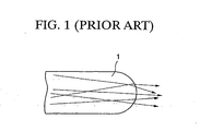
- Moreover, in the case when light emitted from an optical waveguide of one optical wiring substrate is made incident on an optical waveguide of the other optical wiring substrate, it is desirable that the light is rendered parallel in optical path. There is a conventional constitution in which an end face of a
core 1 is formed into a hemispherical shape as shown inFig. 1 , which is intended for rendering parallel light rays passes through the end face. Nevertheless, completely parallel light rays could not be obtained since the light reflected intricately within the optical waveguide. - Furthermore, coupling of hundreds or thousands of optical waveguides on optical wiring substrates may be contemplated by use of optical fiber connectors each fabricated with precision as a connector. However, the number of optical fibers allowable for such a connector is limited to a range from one to about twelve. Accordingly, an enormous number of optical fiber connectors are required for such use, which is unrealistic.
- Since high-speed data transmission is enabled with optical signals, optical communications play a major role in long-distance transmission such as a backbone communication system. In particular, a technology of transmitting different kinds of information simultaneously with different wavelengths in one optical fiber is developed, which is called wavelength division multiplexing (WDM). High-volume information is thereby transmitted in a high speed.
- At a relay station of a backbone communication system, the information sent by WDM is separated into light rays, each having a single wavelength. Then destinations of the individual light rays are switched, and the light rays are again coupled in one optical fiber.
- In this case, a destination of the light ray of any wavelength needs to be switched arbitrarily. That is, a cross-connect function of changing inputs of N channels into outputs of N channels is required.
- As the multiplexing of the WDM develops, it is estimated that 100 or more waves will be sent in one optical fiber. For this reason, the cross-connect function is required for a capability of processing 1,000 channels or more.
- However, an optical switch capable of processing several thousands of channels does not yet exist. Accordingly, practically used are small switches arranged in a multistage combination, as shown in
Fig. 2 . -
Fig. 2 illustrates a state that optical transmission between inputoptical fibers 410 and outputoptical fibers 460 is performed by channel processing of 64 channels of inputs and outputs with two sets ofcross-connect wiring 430 using a three-staged configuration of afirst switch 420, asecond switch 440 and athird switch 450, wherein each switch has 8 x 8 channels. - Each of the switches in respective stages includes a plurality of
optical switches 470, each of which takes charge of a specific number of inputoptical fibers 410. In this case, the cross-connectoptical wiring 430 must have an optical wiring structure in which wires between the switches of the respective stages are connected while intersecting one another. - Heretofore, Japanese Patent Laid-Open
Hei 6 (1994) - 331910 - However, a problem has been pointed out that the switching device requires a huge space for accommodating optical fibers in a case of 1,000 channels or more.
- Accordingly, materialization of an optical wiring substrate that has a cross-connect structure capable of processing transmission of high-speed and high-volume data signals with 1, 000 channels or more is anticipated.
- Meanwhile, Japanese Patent Laid-Open
Hei 11 (1999) - 178018 - The optical connecting device simplifies wiring of the optical fibers therein. However, modes of mounting substrates are limited.
- Moreover, in an optical cross-connect system in Japanese Patent Laid-Open
Hei 10 (1998) - 243424 - Although a compact cross-connect structure is realized, the optical cross-connect system bore a manufacturing problem of an increase of coupling loss unless the lamination was exercisable in a cross-core pitch of optical fibers.
- Moreover, there is also a method of using a fiber sheet technology, in which optical fiber strands are laid into arbitrary wiring and fixed in a sheet form with resin or the like. In this case, compact arrangement is feasible because the optical fibers do not have protection coating.
- However, as previously shown in
Fig. 2 , the optical fibers are accumulated at the central portion of the intersection structure. Whereas a minimum bend radius is defined for the optical fiber, control of the bend radius in a vertical direction generated by lamination of the optical fibers becomes difficult. For this reason, there has been a problem that characteristics of the optical transmission may not be ensured by this method. - Recently, in the field of communications, the optical transmission is becoming a main stream not only for a long-distance signal transmission but also for a short-distance signal transmission. In conventional technologies of electrical signal transmission, clock frequencies and data transmission speeds are increased owing to progress in CPUs. Therefore, signal transmission speeds are improved day by day.
- However, cross-connect devices that take charge of switching signals in the electrical signal transmission technologies are hardly applicable to signal switching for the optical communications without modification. Accordingly, optical via holes are particularly composed between layers of multilayer wiring, thus forming interlayer transfer portion of the optical signals. This interlayer transfer portion has a requirement that orientation of an optical signal therein does not change when an optical path is changed from one layer to another layer via the substrate.
- Moreover, the optical via holes that take charge of switching the optical signals in the multilayer wiring of the optical communications had a risk of causing cracks by stress applied to the inside due to occurrence of air voids by reason of temperature changes during manufacturing processes thereof.
- In addition, in the event that the light enters into the optical via hole from the optical waveguide, the light tends to spread in a progression direction due to wave nature of the light, and thus effective progression of the light in the optical path is impeded.
- Moreover, conventional optical waveguides, which are constituted on an optical wiring substrate for transmitting signals and data in a device for information and communication systems that requires high-speed and high-volume signal transmission, are produced by a process of depositing a cladding material on a substrate such as a silicon wafer, followed by patterning core members.
- In this case, there have been disadvantages such as cambers and cracks of the substrate caused by stress due to thermal hysteresis during the manufacturing steps of the optical waveguides.
- Conventional technologies as countermeasures against such cambers and cracks have been insufficient for multilayer optical wiring substrates. For example, Japanese Patent Laid-Open
Hei 8 (1996) - 29632 - Moreover, Japanese Patent Laid-Open
Hei 5 (1993) - 281424 - On the other hand, Japanese Patent Laid-Open
Hei 6 (1994) - 214128 - Moreover, as a conventional technology for forming a lens on a substrate, known is a manufacturing method of a micro lens as an optical element used for an optical pick-up device for reproducing information out of an optical memory. In Japanese Patent Laid-Open
Sho 60 (1985) - 155552 Hei 11 (1999) - 177123 - However, alignment has been difficult in the event of forming the lenses on the both faces of the substrate.
- For example, as shown in
Fig. 3A , in conventional manufacturing steps of a micro lens used for an optical disk device or the like, in the event of formingconcave portions 62 on both upper and lower faces of asubstrate 61, and of forming lenses by filling theconcave portions 62 withtransparent substance 63 as shown inFig. 3B , a disadvantage of aposition shift 64 due to failure in accurate alignment of the upper and lowerconcave portions 62. Particularly such position shift becomes great when such manufacturing method is used for a large substrate, therefore it is hardly applicable. - In addition, since the substrate needs to be made of an optical material, it has been disadvantageous to form the micro lenses with a large substrate in terms of strength and costs.
- Furthermore, regarding optical signal transmission in a device for information and communication systems that requires high-speed and high-volume signal transmission, optical connection of waveguides of optical wiring substrates requires alignment with high precision at connecting positions thereof, and is also emphasized in terms of enhancing a beam-condensing function thereof.
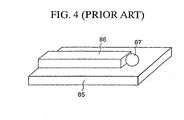
- It is cited that collimating lenses and condenser lenses are required in order to optically connect the optical waveguides with each other. Conventionally known is a structure shown in
Fig. 4 , in which aspherical lens 87 is placed at a tip portion, of which light from a core 86 oncladding 85 is emitted out. - However, the
spherical lens 87 has been required to align with the core 86 at high-precision. Accordingly, in the case where numerous optical waveguides are provided on the wiring substrates, each spherical lens needs to be provided corresponding to each of the optical waveguides. Moreover, in the alignment thereof, the center of thecore 86 is aligned with the center of thespherical lens 87 with high precision of micrometric accuracy. For this reason, the structure resulted in disadvantages of high manufacturing costs as well as complex manufacturing steps. - Moreover, along with improvements in operational frequencies of the CPUs in devices for information and communication systems that require high-speed and high-volume signal transmission, improvements in clock frequencies and data transfer speeds are brought about.
- Recently, high band technologies such as low voltage differential signaling (LVDS) and waveform shaping technology have been developed in order to improve transmission speeds. Although performance of electric transmission have been improved, transmission in a region at 10 Gbps or higher remains difficult because of occurrence of waveform distortion in the electric signals and the like.
- In addition, in the long-distance transmission primarily composed of optical communications, an electric transmissive portion of a cross-connect device that performs path switching cannot fully bear optical communication speeds.
- Consequently, technological developments took place in order to effectuate optical communications also in short-distance transmission, and a connecting mode between an optical transceiver module and an optical fiber has been materialized.
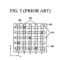
- Moreover, an optical wiring substrate used for optical connections in short-distance and high-speed signal transmission is also known. For example, in a case of constituting multilayer optical wiring by laminating an optical waveguide layer in which a plurality of optical waveguides are arranged parallel to the x-axis direction and an optical waveguide layer in which a plurality of optical waveguides are arranged parallel to the y-axis direction, positions of optical connections between the layers are defined as shown in
Fig. 5 . - In an optical wiring substrate composed of an optical waveguide layer, in which a plurality of
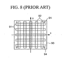
optical waveguides 91 are arranged on anoptical substrate 90 parallel to the x-axis direction, laminated with a plurality ofoptical waveguides 92 arranged parallel to the y-axis direction so that they are orthogonal to the plurality ofoptical waveguides 91, interlayer optical propagation is performed by forming optical via holes at arbitrary intersecting positions 93 illustrated with shades inFig. 5 , selected from respective intersecting points of the plurality of the waveguides along the x-axis and those along the y-axis. - The optical waveguide layer shown in
Fig. 8 , composed by laminating the plurality ofoptical waveguides 91 arranged parallel to the x-axis direction and the plurality ofoptical waveguides 92 arranged parallel to the y-axis direction in order to intersect with one another, can be obtained by laminating an optical waveguide layer shown inFig. 6 that includes the plurality ofoptical waveguides 91 arranged parallel to the x-axis direction with an optical waveguide layer shown inFig. 7 that includes the plurality ofoptical waveguides 92 arranged parallel to the y-axis direction. - Register marks 94 are illustrated on each of the optical waveguide layers, and the multilayer optical wiring shown in
Fig. 8 is obtained by lamination of optical waveguide layers based on the register marks 94. - In the multilayer optical wiring, an intersection structure of optical waveguides and a technique for interlayer connection of optical waveguides should be taken into consideration in order to effectuate wiring arrangements as in a conventional printed substrate.
- In the case of laminating the optical waveguide layers, it is difficult to form the optical via holes, which are interlayer optical transfer portions, onto a substrate having a size of several tens of centimeters or greater for each side, with high accuracy of positioning of several micrometers or less by means of alignment using a conventional photolithographic technology.
- Regarding the example of the conventional art shown in
Fig. 5 , in the case where two optical waveguide layers are laminated, the intersecting positions of the optical waveguides between the layers where the optical via holes are to be formed are indiscernible, because the waveguide layers are transparent. For this reason, lamination is performed based on the register marks 94, and intersecting positions of the patterned optical waveguides are determined as positions for the optical via holes, and laser processing is executed. - However, even if the optical waveguides layers are laminated based on the register marks, the positions for processing the optical via holes may be shifted because of position shifting of the waveguide pattern attributed to a mask for forming the waveguides or position shifting attributed to thermal hysteresis during the process of laminating the waveguides. Such disadvantages become a case of a large size substrate.
- In
JP 04 264409 A - In
DE 44 12 254 A there is discloses an optical coupling member which can be used in integrated optics, which can be produced by conventional technology and which can, if necessary, also deflect passing light, forms with a waveguide a structural component which is integrated monolithically on a substrate and consists of planar thin layers. A cylinder lens lies between the end surface of the waveguide and a Fresnel zone lens which is formed by planar steps disposed in an approximately "cinema-type" arrangement. - An object of the present invention is to provide an optical wiring substrate in which light emitted from an optical waveguide thereof is made as parallel light rays in an optical path, and multilayer optical wiring having an optical connection structure capable of jointing a pair of the optical waveguides without requiring accurate setting of the precision of jointing positions of the pair of the optical waveguides.
- The invention is defined in
claim 1. - With the above-described constitution, in a multilayer wiring substrate of the invention, the parallel light rays obtained from the first optical waveguide via the first slab optical waveguide, the first planar convex lens, the first mirror and the first lens are accurately condensed with the second mirror into the second waveguide. Accordingly, an optical connection between the first and the second waveguides is performed without being bothered by alignment of the waveguides.
-
-
Fig. 1 is a view describing a traveling direction of light in an optical waveguide of a conventional optical wiring board. -
Fig. 2 is a view showing a configuration example of a conventional optical switch having a three-staged configuration, which performs a cross-connect function for multi-channel optical signals. -
Fig. 3A and Fig. 3B are views showing manufacturing steps of a micro lens used for a conventional optical disk device and the like. -
Fig. 4 is a perspective view showing an example of a conventional structure of an optical waveguide. -
Fig. 5 is a schematic plan view showing optical connecting positions in a state that a plurality of optical waveguides are intersected with each other when optical waveguide layers are laminated in a conventional optical wiring substrate. -
Fig. 6 is a plan view showing an arrangement example of a conventional optical waveguide layer in which a plurality of optical waveguides are arranged parallel to the x-axis direction. -
Fig. 7 is a plan, view showing an arrangement example of a conventional optical waveguide layer in which a plurality of optical waveguides are arranged parallel to the y-axis direction. -
Fig. 8 is a plan view showing a conventional optical waveguide layer in which a plurality of optical waveguides are severally arranged parallel to the x-axis direction and the y-axis direction such that they are intersected one another. -
Fig. 9 is a schematic plan view showing a basic constitution of an optical wiring substrate according to a first embodiment of the present invention. -
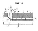
Fig. 10 is a cross-sectional view ofFig. 9 taken along a line I - I. -
Fig. 11 is a partial cross-sectional view showing one optical connection structure of multilayer optical wiring according to the first embodiment of the present invention. - Now, embodiments of the present invention will be described with reference to the accompanying drawings.
-
Fig. 9 is a schematic plan view showing a basic constitution of an optical wiring substrate of the present invention, andFig. 10 is a cross-sectional view ofFig. 9 taken along a line I - I. - An
optical waveguide 10 laid on asubstrate 8 includes acore 1 andcladding 2. Thecore 1, which is a transmitting portion of optical signals, has a refractive index higher than that of thecladding 2. - As a material for the cladding in this case, fluorinated polyimide resin OP1-N3205 (refractive index = 1.52, Hitachi Chemical) is used. As a material for the core, fluorinated polyimide resin OP1-N3405 (refractive index = 1.53, Hitachi Chemical) is used.
- On a tip portion of an optical path of the
core 1 of theoptical waveguide 10, a slaboptical waveguide 3 and a planarconvex lens 4 are continuously formed. - A traveling direction of the light emitted from the
optical waveguide 10 via the slaboptical waveguide 3 and the planarconvex lens 4 is converted by approximately 90° with a 45-degree mirror 5 disposed on the optical path. On a surface of the 45-degree mirror 5, a metallic reflective film or adielectric multilayer film 7 is formed in order to improve reflectivity thereof. - The
dielectric multilayer film 7 in this case has a constitution of alternately layering a high-refractive substance and a low-refractive substance, wherein the products of film thicknesses and refractive indices are set at values of λ/4 or λ/2 (where λ is a wavelength), respectively. ZnS (2.35) or TiO2 (2.35) is used for the high-refractive substance, and meanwhile, MgF2 (1.38) or Si02 (1.46) is used for the low-refractive substance. - A
cylindrical lens 6 for accepting the light reflected with themirror 5 is disposed in a position above themirror 5 on a surface of theoptical waveguide 10. Positioning for disposing thecylindrical lens 6 may be satisfactorily carried out either by providing a cavity on a surface of thecladding 2 or providing apositioning protrusion 9. - In the optical wiring substrate of the above-described constitution, the light traveling from the
core 1 of the optical waveguide diverges in a lateral direction with respect to the traveling direction when passing through theslab waveguide 3, and via the planarconvex lens 4, horizontal components of the light is then emitted as parallel light rays. In this case, an angle of divergence can be made small when the refractive index of theslab waveguide 3 is equal to or larger than the refractive index of thecore 1, whereby the light of parallel rays with a small beam diameter is obtainable. - The traveling direction of the emitted light is converted by approximately 90° with the 45-
degree mirror 5, and the parallel light rays can be obtained via thecylindrical lens 6. Here, a rod lens may substitute for thecylindrical lens 6. -
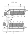
Fig. 11 is a cross-sectional view illustrating an optical connecting structure of multilayer optical wiring, in which light rays emitted from one optical waveguide are rendered parallel in the course of an optical path and are made incident on another optical waveguide, whereby optical waveguides can be coupled with each other without requiring severe setting of accuracy in coupling positions. - In
Fig. 11 , the optical wiring substrate including the one optical waveguide and the optical wiring substrate including the other optical waveguide individually have constitutions identical to the basic constitution of the optical wiring substrate as shown inFig. 10 . Accordingly, the same reference numerals with different indices are affixed thereon, and description for the constitutions thereof will be omitted. - In a position opposite to a
cylindrical lens 6a constituting the one optical wiring substrate, which is present in an optical path, disposed is acylindrical lens 6b constituting the other optical wiring substrate, thus forming an optical connecting structure of the multilayer optical wiring capable of coupling the optical waveguides with each other. - The parallel light rays obtained from the one
cylindrical lens 6a are made incident on thecylindrical lens 6b constituting the other optical wiring substrate to be condensed and inducted toward the other optical waveguide via a 45-degree mirror 7b that converts the optical path thereof by approximately 90 DEG . Subsequently, optical signals are transmitted via a planarconvex lens 4b and aslab waveguide 3b into acore 1b, in series.
Claims (2)
- Multilayer optical wiring comprising:a first optical wiring substrate including:a first substrate (8a);a first optical waveguide (10a) being formed on said first substrate (8a) and including a three-dimensional optical waveguide portion including a core (1a) and cladding (2a) said first optical waveguide (10a) including, a first slab optical waveguide (3a) adjacent to one end of said three-dimensional optical waveguide portion, wherein a first planar convex lens (4a) is provided on the optical path of said first optical waveguide (10a) and is continuously formed at a tip portion of said first optical waveguide (10a), the first planar convex lens (4a) being formed integrally with the first slab optical waveguide (3a) ;a first mirror (5a) arranged for reflecting the light which is transmitted through said first planar convex lens (4a) toward a direction intersecting a face of said substrate (8a); anda first lens (6a) arranged so that said light reflected by said first mirror (5a) is made as parallel light rays, andwherein the first planar convex lens (4a) is adapted to collimate light transmitted through the first slab optical waveguide from the core in a direction parallel with the face of the substrate (8a), andwherein the first lens (6a) is a cylindrical lens having an elongated direction arranged to extend in a direction perpendicular to the direction of the collimated light emitted from the first planar convex lens (4a), and perpendicular to the propagation direction of the light reflected from the first mirror (5a), anda second optical wiring substrate including:a second substrate (8b);a second optical waveguide (10b) being formed on said second substrate (8b) and including a three-dimensional optical waveguide portion including a core (1b) and a cladding (2b) said second optical waveguide (10b) including, a second slab optical waveguide (3b) adjacent to one end of said three-dimensional optical waveguide portion, wherein a second planar convex lens (4b) is provided on the optical path of said second optical waveguide (10b) and is continuously formed at a tip portionof said second optical waveguide (10b), the second planar convex lens (4b) being formed integrally with the second slab optical waveguide (3b) ;a second lens (6b) disposed opposite to said first lens (6a)and arranged for allowing the parallel light rays from said first lens (6a) to be made incident and condensed;a second mirror (5b) arranged for reflecting the light which is transmitted through said second lens (5b) toward a direction parallel to a face of said second substrate (8b);wherein the second planar convex lens (4b) is adapted to collimate light transmitted through the second slab optical waveguide from the core in a direction parallel with the face of the second substrate (8b), and
wherein the second lens (6b) is a cylindrical lens having an elongated direction arranged to extend in a direction perpendicular to the direction of the collimated light emitted from the second planar convex lens (4b), and perpendicular to a propagation direction of the light reflected from the second mirror (5b),
and wherein the second planar convex lens (4b) and the second optical waveguide (10b) are positioned so that the light reflected by said second mirror (5b) is coupled therethrough, and
wherein the first and second optical wiring substrates are arranged sot that optical signals are connected between said first optical wiring substrate and said second optical wiring substrate. - The optical wiring substrate according to claim 1, wherein any one of a metallic reflective film and a dielectric multilayer film is formed on a surface of said mirror (5).
Applications Claiming Priority (2)
| Application Number | Priority Date | Filing Date | Title |
|---|---|---|---|
| JP2001056009A JP2002258081A (en) | 2001-02-28 | 2001-02-28 | Optical wiring board, manufacturing method of the same, and multi-layer optical wiring |
| JP2001056009 | 2001-02-28 |
Publications (3)
| Publication Number | Publication Date |
|---|---|
| EP1237019A2 EP1237019A2 (en) | 2002-09-04 |
| EP1237019A3 EP1237019A3 (en) | 2004-05-19 |
| EP1237019B1 true EP1237019B1 (en) | 2009-04-08 |
Family
ID=18916104
Family Applications (1)
| Application Number | Title | Priority Date | Filing Date |
|---|---|---|---|
| EP02004268A Expired - Lifetime EP1237019B1 (en) | 2001-02-28 | 2002-02-27 | Optical coupling between optical wiring substrates |
Country Status (5)
| Country | Link |
|---|---|
| US (2) | US6810160B2 (en) |
| EP (1) | EP1237019B1 (en) |
| JP (1) | JP2002258081A (en) |
| CA (1) | CA2373564C (en) |
| DE (1) | DE60231848D1 (en) |
Cited By (1)
| Publication number | Priority date | Publication date | Assignee | Title |
|---|---|---|---|---|
| CN1605887B (en) * | 2003-10-06 | 2010-04-28 | 三井化学株式会社 | Optical waveguide having specular surface formed by laser beam machining |
Families Citing this family (116)
| Publication number | Priority date | Publication date | Assignee | Title |
|---|---|---|---|---|
| US6665495B1 (en) * | 2000-10-27 | 2003-12-16 | Yotta Networks, Inc. | Non-blocking, scalable optical router architecture and method for routing optical traffic |
| JP4433608B2 (en) * | 2000-12-28 | 2010-03-17 | 株式会社トッパンNecサーキットソリューションズ | Optical module and manufacturing method thereof |
| US6771846B2 (en) * | 2001-04-17 | 2004-08-03 | Lucent Technologies Inc. | Optical interconnect for mezzanine circuit boards |
| US6771867B2 (en) * | 2002-02-05 | 2004-08-03 | Mitsubishi Chemical Corporation | Optical memory device and method for fabricating optical memory device, and method and apparatus for lamination with filmy member |
| JP3768901B2 (en) | 2002-02-28 | 2006-04-19 | 松下電器産業株式会社 | Manufacturing method of three-dimensional optical waveguide |
| JP3833131B2 (en) * | 2002-03-25 | 2006-10-11 | キヤノン株式会社 | Optical transmission equipment |
| US6832034B2 (en) * | 2002-06-21 | 2004-12-14 | 3M Innovative Properties Company | Optical waveguide |
| CA2471963C (en) * | 2002-09-20 | 2012-07-10 | Toppan Printing Co., Ltd. | Optical waveguide and method of manufacturing the same |
| US6912335B2 (en) * | 2003-01-10 | 2005-06-28 | Agilent Technologies, Inc. | Optical switch with reduced beam divergence |
| US7263248B2 (en) * | 2003-02-11 | 2007-08-28 | Avago Technologies Fiber Ip (Singapore) Pte. Ltd. | Optical via to pass signals through a printed circuit board |
| US7786983B2 (en) * | 2003-04-08 | 2010-08-31 | Poa Sana Liquidating Trust | Apparatus and method for a data input device using a light lamina screen |
| US7272293B2 (en) * | 2003-08-12 | 2007-09-18 | Omnitek Partners Llc | Device having a casing and /or interior acting as a communication bus between electronic components |
| JP4659422B2 (en) * | 2003-10-06 | 2011-03-30 | 三井化学株式会社 | Manufacturing method of optical waveguide |
| US7218812B2 (en) | 2003-10-27 | 2007-05-15 | Rpo Pty Limited | Planar waveguide with patterned cladding and method for producing the same |
| JP2005148468A (en) * | 2003-11-17 | 2005-06-09 | Sony Corp | Optical waveguide, light source module and optical information processing device |
| JP3887371B2 (en) * | 2003-11-27 | 2007-02-28 | インターナショナル・ビジネス・マシーンズ・コーポレーション | Optical transmission board, optical transmission board manufacturing method, and opto-electric integrated circuit |
| US7509011B2 (en) * | 2004-01-15 | 2009-03-24 | Poa Sana Liquidating Trust | Hybrid waveguide |
| US6996303B2 (en) * | 2004-03-12 | 2006-02-07 | Fujitsu Limited | Flexible optical waveguides for backplane optical interconnections |
| JP4308050B2 (en) | 2004-03-18 | 2009-08-05 | 三洋電機株式会社 | Optical waveguide |
| US7251393B2 (en) * | 2004-03-30 | 2007-07-31 | Lockheed Martin Corporation | Optical router |
| US7267930B2 (en) * | 2004-06-04 | 2007-09-11 | National Semiconductor Corporation | Techniques for manufacturing a waveguide with a three-dimensional lens |
| US7676131B2 (en) * | 2004-06-04 | 2010-03-09 | Poa Sana Liquidating Trust | Waveguide with a three-dimensional lens |
| US7471865B2 (en) | 2004-06-04 | 2008-12-30 | Poa Sana Liquidating Trust | Apparatus and method for a molded waveguide for use with touch screen displays |
| US7236666B2 (en) * | 2004-09-30 | 2007-06-26 | Intel Corporation | On-substrate microlens to couple an off-substrate light emitter and/or receiver with an on-substrate optical device |
| US7391937B2 (en) * | 2004-10-22 | 2008-06-24 | Lockheed Martin Corporation | Compact transition in layered optical fiber |
| JP2006126658A (en) * | 2004-10-29 | 2006-05-18 | Nippon Telegr & Teleph Corp <Ntt> | Optical waveguide device |
| WO2006059510A1 (en) * | 2004-12-02 | 2006-06-08 | Mitsui Chemicals, Inc. | Optical wiring substrate and optical and electric combined substrate |
| JP5005168B2 (en) * | 2004-12-06 | 2012-08-22 | ソニー株式会社 | Optical waveguide device, manufacturing method thereof, optical information processing device, and electronic apparatus |
| JP2006171642A (en) * | 2004-12-20 | 2006-06-29 | Sony Corp | Optical waveguide sheet, optoelectronic apparatus and their manufacturing method |
| JP2006215289A (en) * | 2005-02-03 | 2006-08-17 | Mitsui Chemicals Inc | Substrate for optical circuit, and manufacturing method of optical circuit substrate using the same |
| JP2006243013A (en) * | 2005-02-28 | 2006-09-14 | Nippon Telegr & Teleph Corp <Ntt> | Multi-port optical switch |
| US8272758B2 (en) | 2005-06-07 | 2012-09-25 | Oree, Inc. | Illumination apparatus and methods of forming the same |
| US8215815B2 (en) | 2005-06-07 | 2012-07-10 | Oree, Inc. | Illumination apparatus and methods of forming the same |
| US8128272B2 (en) | 2005-06-07 | 2012-03-06 | Oree, Inc. | Illumination apparatus |
| US7551814B1 (en) | 2006-02-21 | 2009-06-23 | National Semiconductor Corporation | Optical detection of user interaction based on external light source |
| CN101389991B (en) * | 2006-02-22 | 2010-12-08 | 艾迪株式会社 | Low loss funnel-type plc optical splitter with input cladding mode absorption structure and/or output segmented taper structure |
| US7474815B2 (en) * | 2006-03-14 | 2009-01-06 | International Business Machines Corporation | Interconnecting (mapping) a two-dimensional optoelectronic (OE) device array to a one-dimensional waveguide array |
| JP4759423B2 (en) * | 2006-03-27 | 2011-08-31 | 富士通株式会社 | Optical transmission system |
| JPWO2007114316A1 (en) * | 2006-03-30 | 2009-08-20 | 京セラ株式会社 | OPTICAL TRANSMISSION BOARD, MANUFACTURING METHOD THEREOF, AND OPTICAL ELECTRONIC HYBRID SUBSTRATE |
| US20080031584A1 (en) * | 2006-08-02 | 2008-02-07 | National Semiconductor Corporation | Apparatus and method for a singulation of polymer waveguides using photolithography |
| JP5078442B2 (en) * | 2006-09-27 | 2012-11-21 | 京セラ株式会社 | OPTICAL TRANSMISSION BOARD, MANUFACTURING METHOD THEREOF, OPTICAL ELECTRONIC HYBRID SUBSTRATE, AND OPTICAL MODULE |
| US7369724B2 (en) | 2006-10-03 | 2008-05-06 | National Semiconductor Corporation | Apparatus and method for an improved lens structure for polymer wave guides which maximizes free space light coupling |
| JP4864761B2 (en) * | 2007-02-19 | 2012-02-01 | 日東電工株式会社 | Optical waveguide for touch panel |
| JP5018254B2 (en) * | 2007-06-06 | 2012-09-05 | 日立電線株式会社 | Optical waveguide with mirror and manufacturing method thereof |
| US20100183302A1 (en) * | 2007-06-08 | 2010-07-22 | Research Triangle Institute | Optical switch |
| US7646949B2 (en) * | 2007-07-27 | 2010-01-12 | Kotura, Inc. | Efficient transfer of light signals between optical devices |
| JP4767228B2 (en) * | 2007-07-30 | 2011-09-07 | 京セラ株式会社 | OPTICAL TRANSMISSION SUBSTRATE AND METHOD FOR MANUFACTURING THE SAME, OPTICAL TRANSMISSION DEVICE, COMPOSITE OPTICAL TRANSMISSION BOARD |
| EP2217955B1 (en) | 2007-11-30 | 2017-08-16 | Dow Corning Corporation | An integrated planar polymer waveguide for low-loss, low-crosstalk optical signal routing |
| US7929816B2 (en) * | 2007-12-19 | 2011-04-19 | Oree, Inc. | Waveguide sheet containing in-coupling, propagation, and out-coupling regions |
| US8172447B2 (en) | 2007-12-19 | 2012-05-08 | Oree, Inc. | Discrete lighting elements and planar assembly thereof |
| JP4452305B2 (en) * | 2007-12-25 | 2010-04-21 | 日東電工株式会社 | Optical waveguide for touch panel, touch panel using the same, and method for manufacturing optical waveguide for touch panel |
| US7945131B1 (en) | 2008-01-11 | 2011-05-17 | Kotusa, Inc. | System having optical amplifier incorporated into stacked optical devices |
| EP2260341A2 (en) | 2008-03-05 | 2010-12-15 | Oree, Advanced Illumination Solutions INC. | Illumination apparatus and methods of forming the same |
| US8200051B2 (en) * | 2008-03-24 | 2012-06-12 | Nitto Denko Corporation | Apparatus using waveguide, optical touch panel, and method of fabricating waveguide |
| US8090231B1 (en) | 2008-04-21 | 2012-01-03 | Kotura, Inc. | Transfer of light signals between optical fibers and system using optical devices with optical vias |
| KR101251028B1 (en) | 2008-04-26 | 2013-04-04 | 광주과학기술원 | Optical connection structure and method for fabricating the same |
| KR101394844B1 (en) * | 2008-05-09 | 2014-05-14 | 휴렛-팩커드 디벨롭먼트 컴퍼니, 엘.피. | Proximity free space optical interconnect |
| US8297786B2 (en) | 2008-07-10 | 2012-10-30 | Oree, Inc. | Slim waveguide coupling apparatus and method |
| US8301002B2 (en) | 2008-07-10 | 2012-10-30 | Oree, Inc. | Slim waveguide coupling apparatus and method |
| JP5109982B2 (en) * | 2008-10-09 | 2012-12-26 | 日立電線株式会社 | Manufacturing method of optical transmission body with mirror |
| ES2717200T3 (en) * | 2008-12-12 | 2019-06-19 | Bae Systems Plc | Improvements in waveguides or related to these |
| TWI522668B (en) * | 2009-02-25 | 2016-02-21 | Hitachi Chemical Co Ltd | Optical waveguide and optical waveguide module |
| JP5498219B2 (en) * | 2009-03-26 | 2014-05-21 | パナソニック株式会社 | Manufacturing method of optical waveguide having mirror surface and photoelectric composite wiring board |
| US8624527B1 (en) | 2009-03-27 | 2014-01-07 | Oree, Inc. | Independently controllable illumination device |
| WO2010129536A2 (en) * | 2009-05-04 | 2010-11-11 | University Of Delaware | System and method for free-space optical interconnections |
| US8328406B2 (en) | 2009-05-13 | 2012-12-11 | Oree, Inc. | Low-profile illumination device |
| US8727597B2 (en) | 2009-06-24 | 2014-05-20 | Oree, Inc. | Illumination apparatus with high conversion efficiency and methods of forming the same |
| JP2011085916A (en) * | 2009-09-15 | 2011-04-28 | Ricoh Co Ltd | Multibeam deflector, two dimensional scanner, and multibeam deflector module |
| US8620122B2 (en) * | 2010-09-10 | 2013-12-31 | Avago Technologies General Ip (Singapore) Pte. Ltd. | Low-profile optical communications module having two generally flat optical connector modules that slidingly engage one another |
| US8909007B2 (en) * | 2010-10-29 | 2014-12-09 | Hewlett-Packard Development Company, L.P. | Circuit switchable optical device |
| KR20120048258A (en) * | 2010-11-05 | 2012-05-15 | 한국전자통신연구원 | Optical waveguide structure equipped with angled mirror and lens |
| KR20120056411A (en) * | 2010-11-25 | 2012-06-04 | 한국전자통신연구원 | Optical Module Comprising Optical Hybrid Using Metal Waveguide and Photo Detector |
| US9116319B2 (en) * | 2010-12-17 | 2015-08-25 | Stmicroelectronics, Inc. | Photonic integrated circuit having a plurality of lenses |
| CN102809784B (en) * | 2011-06-02 | 2014-08-27 | 富士康(昆山)电脑接插件有限公司 | Light back plate assembly |
| JP2013003224A (en) * | 2011-06-14 | 2013-01-07 | Shinko Electric Ind Co Ltd | Optical waveguide, manufacturing method thereof, and optical waveguide device |
| US8818145B2 (en) * | 2011-08-03 | 2014-08-26 | Tyco Electronics Corporation | Optical interposer with transparent substrate |
| US20130094804A1 (en) * | 2011-10-13 | 2013-04-18 | Alcatel-Lucent, Usa Inc. | Optical switch |
| US8591072B2 (en) | 2011-11-16 | 2013-11-26 | Oree, Inc. | Illumination apparatus confining light by total internal reflection and methods of forming the same |
| EP2804033A4 (en) * | 2012-01-10 | 2015-08-19 | Hitachi Chemical Co Ltd | Optical waveguide with mirror, optical fiber connector, and manufacturing method thereof |
| TWI575270B (en) * | 2012-01-11 | 2017-03-21 | Hitachi Chemical Co Ltd | Optical waveguide and its manufacturing method |
| CN104126138A (en) * | 2012-02-27 | 2014-10-29 | 住友电木株式会社 | Optical waveguide, optical wiring component, optical waveguide module and electronic device |
| JP5877749B2 (en) | 2012-03-29 | 2016-03-08 | 日東電工株式会社 | Manufacturing method of opto-electric hybrid board |
| TW201346371A (en) * | 2012-05-04 | 2013-11-16 | Hon Hai Prec Ind Co Ltd | Optical fiber coupled connector and method for making same |
| US9229163B2 (en) * | 2012-05-18 | 2016-01-05 | Oracle International Corporation | Butterfly optical network with crossing-free switches |
| JP5964143B2 (en) * | 2012-05-31 | 2016-08-03 | 日本メクトロン株式会社 | Manufacturing method of opto-electric hybrid printed wiring board |
| US9857519B2 (en) | 2012-07-03 | 2018-01-02 | Oree Advanced Illumination Solutions Ltd. | Planar remote phosphor illumination apparatus |
| JP2014041181A (en) * | 2012-08-21 | 2014-03-06 | Hitachi Chemical Co Ltd | Substrate with lens and production method therefor, and optical waveguide with lens |
| US9490148B2 (en) * | 2012-09-27 | 2016-11-08 | Taiwan Semiconductor Manufacturing Company, Ltd. | Adhesion promoter apparatus and method |
| US9052464B1 (en) * | 2013-01-18 | 2015-06-09 | Kotura, Inc. | Transfer of light signals between optical devices |
| US9124959B2 (en) * | 2013-08-05 | 2015-09-01 | Telefonaktiebolaget L M Ericsson (Publ) | High connectivity multiple dimension optical network in glass |
| US9077450B2 (en) * | 2013-09-06 | 2015-07-07 | International Business Machines Corporation | Wavelength division multiplexing with multi-core fiber |
| US9086551B2 (en) * | 2013-10-30 | 2015-07-21 | International Business Machines Corporation | Double mirror structure for wavelength division multiplexing with polymer waveguides |
| NL2013524B1 (en) * | 2014-09-25 | 2016-09-07 | Anteryon Wafer Optics B V | An optical light guide element and a method for manufacturing. |
| CN106662709A (en) * | 2014-09-30 | 2017-05-10 | 株式会社藤仓 | Substrate-type optical waveguide element and method for producing substrate-type optical waveguide element |
| JP6314240B2 (en) | 2014-09-30 | 2018-04-18 | 株式会社フジクラ | Substrate type optical waveguide device |
| US9543463B2 (en) | 2014-10-27 | 2017-01-10 | International Business Machines Corporation | Signal distribution in integrated circuit using optical through silicon via |
| JP6455831B2 (en) * | 2014-11-25 | 2019-01-23 | インターナショナル・ビジネス・マシーンズ・コーポレーションInternational Business Machines Corporation | Optical communication module |
| JP6471502B2 (en) | 2015-01-08 | 2019-02-20 | 富士通株式会社 | Optical axis adjustment method for optical interconnection and optical interconnection substrate |
| US9583912B2 (en) * | 2015-05-20 | 2017-02-28 | Hc Photonics Corp. | Compact optical and laser systems and ultrafast laser utilizing the same |
| EP3345029A1 (en) * | 2015-09-04 | 2018-07-11 | CCS Technology, Inc. | Fiber coupling device for coupling of at last one optical fiber |
| US9804334B2 (en) * | 2015-10-08 | 2017-10-31 | Teramount Ltd. | Fiber to chip optical coupler |
| US11585991B2 (en) | 2019-02-28 | 2023-02-21 | Teramount Ltd. | Fiberless co-packaged optics |
| US20230296853A9 (en) | 2015-10-08 | 2023-09-21 | Teramount Ltd. | Optical Coupling |
| US10564374B2 (en) | 2015-10-08 | 2020-02-18 | Teramount Ltd. | Electro-optical interconnect platform |
| JP2018010030A (en) * | 2016-07-11 | 2018-01-18 | 富士通コンポーネント株式会社 | Optical module |
| TWI743188B (en) | 2016-09-20 | 2021-10-21 | 新加坡商新加坡恒立私人有限公司 | Optical device, compound optical device have the same, and method for manufacturing the same |
| US10359565B2 (en) * | 2017-02-07 | 2019-07-23 | Nokia Of America Corporation | Optoelectronic circuit having one or more double-sided substrates |
| US10436991B2 (en) | 2017-05-19 | 2019-10-08 | Adolite Inc. | Optical interconnect modules based on glass substrate with polymer waveguide |
| CN108700718A (en) * | 2017-11-15 | 2018-10-23 | 索尔思光电(成都)有限公司 | Waveguide array module and the sub- device of light-receiving |
| US11036321B2 (en) * | 2018-07-27 | 2021-06-15 | Lg Display Co., Ltd. | Light control film and display apparatus including the same |
| US11886001B2 (en) * | 2019-12-20 | 2024-01-30 | Snap Inc. | Optical waveguide fabrication process |
| DE112021004425T5 (en) | 2020-10-23 | 2023-06-29 | Apple Inc. | FAST-AXIS COLLIMATOR WITH PENDANT CONNECTOR |
| EP3995871A1 (en) | 2020-11-09 | 2022-05-11 | Imec VZW | Two-stage expanded beam optical coupling |
| KR20240043812A (en) * | 2021-09-23 | 2024-04-03 | 애플 인크. | Light output devices and light output methods for optical systems |
| FR3132786A1 (en) * | 2022-02-14 | 2023-08-18 | Stmicroelectronics (Crolles 2) Sas | METHOD FOR FABRICATING A SEMICONDUCTOR DEVICE |
| WO2024028942A1 (en) * | 2022-08-01 | 2024-02-08 | 日本電信電話株式会社 | Optical cross-connect device and method for manufacturing same |
Citations (4)
| Publication number | Priority date | Publication date | Assignee | Title |
|---|---|---|---|---|
| WO1988005970A1 (en) * | 1987-02-02 | 1988-08-11 | University Of Delaware | Dual mode laser/detector diode for optical fiber transmission lines |
| JPH04264409A (en) * | 1991-02-19 | 1992-09-21 | Nippon Telegr & Teleph Corp <Ntt> | Optical coupling circuit |
| DE4412254A1 (en) * | 1994-04-07 | 1995-10-12 | Hertz Inst Heinrich | Optical coupling element and method for its production |
| US5606181A (en) * | 1994-03-29 | 1997-02-25 | Ricoh Company, Ltd. | Edge emitting type light emitting diode array heads |
Family Cites Families (40)
| Publication number | Priority date | Publication date | Assignee | Title |
|---|---|---|---|---|
| JPS58211717A (en) * | 1982-06-04 | 1983-12-09 | Fujitsu Ltd | Composite optical waveguide |
| JPS60155552A (en) * | 1984-01-24 | 1985-08-15 | Oki Electric Ind Co Ltd | Production of plate microlens |
| JPS6235304A (en) * | 1985-08-09 | 1987-02-16 | Nippon Telegr & Teleph Corp <Ntt> | Optical waveguide circuit with lens and its manufacture |
| US4732446A (en) * | 1985-10-02 | 1988-03-22 | Lamar Gipson | Electrical circuit and optical data buss |
| GB8727212D0 (en) | 1987-11-20 | 1987-12-23 | Secr Defence | Optical beam steering device |
| JPH03119782A (en) * | 1989-10-02 | 1991-05-22 | Fujitsu Ltd | Optical semiconductor device |
| EP0498169B1 (en) * | 1991-02-08 | 1995-12-20 | Siemens Aktiengesellschaft | Opto-electronic device for coupling and uncoupling of radiation |
| US5263111A (en) * | 1991-04-15 | 1993-11-16 | Raychem Corporation | Optical waveguide structures and formation methods |
| US5168401A (en) * | 1991-05-07 | 1992-12-01 | Spectra Diode Laboratories, Inc. | Brightness conserving optical system for modifying beam symmetry |
| DE4204391A1 (en) * | 1992-02-14 | 1993-08-19 | Rheinmetall Gmbh | CIRCUIT BOARD FOR A POWER SEMICONDUCTOR POWER ELECTRONIC CIRCUIT |
| US5253319A (en) * | 1992-02-24 | 1993-10-12 | Corning Incorporated | Planar optical waveguides with planar optical elements |
| JPH05241044A (en) | 1992-03-02 | 1993-09-21 | Nippon Telegr & Teleph Corp <Ntt> | Optical coupling system between optical element and optical waveguide |
| JPH05281424A (en) * | 1992-04-03 | 1993-10-29 | Fujikura Ltd | Substrate type optical waveguide |
| JPH06214128A (en) * | 1993-01-19 | 1994-08-05 | Nippon Telegr & Teleph Corp <Ntt> | Optical waveguide circuit |
| JPH06250031A (en) | 1993-02-24 | 1994-09-09 | Nec Commun Syst Ltd | Optical wiring board |
| JPH06331910A (en) * | 1993-05-24 | 1994-12-02 | Nippon Telegr & Teleph Corp <Ntt> | Coated optical fiber switching device |
| US5381506A (en) * | 1993-10-18 | 1995-01-10 | Mcdonnell Douglas Corporation | Flat to spiral polymer light waveguide |
| JP3617853B2 (en) | 1994-07-14 | 2005-02-09 | 住友電気工業株式会社 | Optical waveguide |
| JPH08179178A (en) | 1994-12-27 | 1996-07-12 | Canon Inc | Optical module |
| US5513196A (en) * | 1995-02-14 | 1996-04-30 | Deacon Research | Optical source with mode reshaping |
| JPH09283776A (en) | 1996-04-17 | 1997-10-31 | Yokogawa Electric Corp | Photodetector |
| JP3144627B2 (en) | 1996-09-02 | 2001-03-12 | 日本電信電話株式会社 | Optical switch and method of assembling the same |
| JP3349938B2 (en) * | 1996-12-27 | 2002-11-25 | 日本電信電話株式会社 | Optical cross connect system |
| US5841917A (en) * | 1997-01-31 | 1998-11-24 | Hewlett-Packard Company | Optical cross-connect switch using a pin grid actuator |
| DE19742895C2 (en) * | 1997-09-24 | 1999-10-21 | Siemens Ag | Electro-optical arrangement |
| JPH11248954A (en) | 1998-03-06 | 1999-09-17 | Nippon Telegr & Teleph Corp <Ntt> | Optical hybrid module |
| US6058228A (en) * | 1997-10-06 | 2000-05-02 | Nec Research Institute, Inc. | Cost-effective side-coupling polymer fiber optics for optical interconnections |
| JPH11178018A (en) * | 1997-12-11 | 1999-07-02 | Oki Electric Ind Co Ltd | Optical cross connector |
| JPH11177123A (en) * | 1997-12-12 | 1999-07-02 | Ricoh Co Ltd | Manufacture of optical element for optical pickup |
| JP3715425B2 (en) * | 1998-03-06 | 2005-11-09 | ブラザー工業株式会社 | Manufacturing method of substrate with optical waveguide |
| JP2000275449A (en) * | 1999-03-25 | 2000-10-06 | Minolta Co Ltd | Optical waveguide |
| DE19947889C2 (en) * | 1999-10-05 | 2003-03-06 | Infineon Technologies Ag | Optoelectronic, bidirectional transmit and receive module in leadframe technology |
| JP2001174671A (en) * | 1999-12-16 | 2001-06-29 | Japan Aviation Electronics Industry Ltd | Optical element module |
| US6328484B1 (en) * | 2000-03-02 | 2001-12-11 | Agilent Technologies, Inc. | Fiber optic lens system for coupling fibers to surface mounted devices |
| US6501869B1 (en) * | 2000-03-20 | 2002-12-31 | George Mason University | Optical switching system |
| JP2001281486A (en) * | 2000-03-30 | 2001-10-10 | Japan Aviation Electronics Industry Ltd | Film optical waveguide and method for manufacturing the same |
| KR100382652B1 (en) * | 2001-03-07 | 2003-05-09 | 삼성전자주식회사 | A optical bench |
| US6529653B1 (en) * | 2001-04-11 | 2003-03-04 | Optical Switch Corporation | System and method for orienting and positioning optical fibers |
| US6842573B2 (en) * | 2001-07-05 | 2005-01-11 | Hudson Research Inc. | Directional optical coupler |
| US6738541B2 (en) * | 2001-09-18 | 2004-05-18 | Agilent Technologies, Inc. | Optical switch comprising two non-coplanar arrays of optical waveguides |
-
2001
- 2001-02-28 JP JP2001056009A patent/JP2002258081A/en active Pending
-
2002
- 2002-02-26 CA CA002373564A patent/CA2373564C/en not_active Expired - Fee Related
- 2002-02-27 DE DE60231848T patent/DE60231848D1/en not_active Expired - Lifetime
- 2002-02-27 EP EP02004268A patent/EP1237019B1/en not_active Expired - Lifetime
- 2002-02-28 US US10/086,945 patent/US6810160B2/en not_active Expired - Fee Related
-
2004
- 2004-09-24 US US10/949,906 patent/US7068871B2/en not_active Expired - Fee Related
Patent Citations (4)
| Publication number | Priority date | Publication date | Assignee | Title |
|---|---|---|---|---|
| WO1988005970A1 (en) * | 1987-02-02 | 1988-08-11 | University Of Delaware | Dual mode laser/detector diode for optical fiber transmission lines |
| JPH04264409A (en) * | 1991-02-19 | 1992-09-21 | Nippon Telegr & Teleph Corp <Ntt> | Optical coupling circuit |
| US5606181A (en) * | 1994-03-29 | 1997-02-25 | Ricoh Company, Ltd. | Edge emitting type light emitting diode array heads |
| DE4412254A1 (en) * | 1994-04-07 | 1995-10-12 | Hertz Inst Heinrich | Optical coupling element and method for its production |
Cited By (1)
| Publication number | Priority date | Publication date | Assignee | Title |
|---|---|---|---|---|
| CN1605887B (en) * | 2003-10-06 | 2010-04-28 | 三井化学株式会社 | Optical waveguide having specular surface formed by laser beam machining |
Also Published As
| Publication number | Publication date |
|---|---|
| US6810160B2 (en) | 2004-10-26 |
| DE60231848D1 (en) | 2009-05-20 |
| JP2002258081A (en) | 2002-09-11 |
| CA2373564A1 (en) | 2002-08-28 |
| US7068871B2 (en) | 2006-06-27 |
| US20020118907A1 (en) | 2002-08-29 |
| EP1237019A3 (en) | 2004-05-19 |
| EP1237019A2 (en) | 2002-09-04 |
| CA2373564C (en) | 2007-05-08 |
| US20050041906A1 (en) | 2005-02-24 |
Similar Documents
| Publication | Publication Date | Title |
|---|---|---|
| EP1237019B1 (en) | Optical coupling between optical wiring substrates | |
| JP3883901B2 (en) | Optical path conversion device and manufacturing method thereof | |
| EP2261709B1 (en) | Optical coupling device with optical waveguide coupled to optical device | |
| EP0309102B1 (en) | Micro-optical building block system and method of making same | |
| KR101305848B1 (en) | Optical waveguide and optical waveguide module | |
| US20070230868A1 (en) | Optical reflector, optical system and optical multiplexer/demultiplexer device | |
| JPH09200187A (en) | Waveguide grating type optical demultiplexer and its method of use | |
| US5000530A (en) | Optical multiplexing/demultiplexing device with multiple ports | |
| US7349593B2 (en) | Optical wavelength switch having planar lightwave circuit structure | |
| JPH08313744A (en) | Optical circuit parts | |
| WO2019244554A1 (en) | Planar lightwave circuit and optical device | |
| JPH10300956A (en) | Optical branching waveguide and optical waveguide circuit | |
| JP2002131566A (en) | Optical part having optical waveguide interval converting part, optical circuit and method for manufacturing optical circuit | |
| JP4283048B2 (en) | Light control module | |
| JP2002258084A (en) | Light-wave circuit module and method of manufacturing the same | |
| JP5163608B2 (en) | Optical coupling structure and method of manufacturing electrical wiring board | |
| JP2005249966A (en) | Optical member, its manufacturing method, and optical module | |
| WO2023218607A1 (en) | Optical circuit chip | |
| JP3886840B2 (en) | Optical path conversion device | |
| JP2001337246A (en) | Optical waveguide parts, method for manufacturing optical waveguide parts, connecting member, optical parts, method for connecting optical waveguide parts and optical element | |
| WO2007007073A1 (en) | Three dimensional optical path control by integrating rotated structures | |
| JP2003329864A (en) | Optical substrate having slab waveguide and hybrid type optical integrated circuit device | |
| JPH1138243A (en) | Optical branching waveguide | |
| JP2003050333A (en) | Optical wiring substrate and optical cross connect device | |
| KR20050094418A (en) | Optical device and method for fabricating the same |
Legal Events
| Date | Code | Title | Description |
|---|---|---|---|
| PUAI | Public reference made under article 153(3) epc to a published international application that has entered the european phase |
Free format text: ORIGINAL CODE: 0009012 |
|
| AK | Designated contracting states |
Kind code of ref document: A2 Designated state(s): AT BE CH CY DE DK ES FI FR GB GR IE IT LI LU MC NL PT SE TR |
|
| AX | Request for extension of the european patent |
Free format text: AL;LT;LV;MK;RO;SI |
|
| PUAL | Search report despatched |
Free format text: ORIGINAL CODE: 0009013 |
|
| AK | Designated contracting states |
Kind code of ref document: A3 Designated state(s): AT BE CH CY DE DK ES FI FR GB GR IE IT LI LU MC NL PT SE TR |
|
| AX | Request for extension of the european patent |
Extension state: AL LT LV MK RO SI |
|
| 17P | Request for examination filed |
Effective date: 20040917 |
|
| AKX | Designation fees paid |
Designated state(s): DE FR GB |
|
| 17Q | First examination report despatched |
Effective date: 20060124 |
|
| RTI1 | Title (correction) |
Free format text: OPTICAL COUPLING BETWEEN OPTICAL WIRING SUBSTRATES |
|
| GRAP | Despatch of communication of intention to grant a patent |
Free format text: ORIGINAL CODE: EPIDOSNIGR1 |
|
| GRAS | Grant fee paid |
Free format text: ORIGINAL CODE: EPIDOSNIGR3 |
|
| GRAA | (expected) grant |
Free format text: ORIGINAL CODE: 0009210 |
|
| AK | Designated contracting states |
Kind code of ref document: B1 Designated state(s): DE FR GB |
|
| REG | Reference to a national code |
Ref country code: GB Ref legal event code: FG4D |
|
| REF | Corresponds to: |
Ref document number: 60231848 Country of ref document: DE Date of ref document: 20090520 Kind code of ref document: P |
|
| PLBE | No opposition filed within time limit |
Free format text: ORIGINAL CODE: 0009261 |
|
| STAA | Information on the status of an ep patent application or granted ep patent |
Free format text: STATUS: NO OPPOSITION FILED WITHIN TIME LIMIT |
|
| 26N | No opposition filed |
Effective date: 20100111 |
|
| GBPC | Gb: european patent ceased through non-payment of renewal fee |
Effective date: 20100227 |
|
| PG25 | Lapsed in a contracting state [announced via postgrant information from national office to epo] |
Ref country code: GB Free format text: LAPSE BECAUSE OF NON-PAYMENT OF DUE FEES Effective date: 20100227 |
|
| PGFP | Annual fee paid to national office [announced via postgrant information from national office to epo] |
Ref country code: DE Payment date: 20110223 Year of fee payment: 10 Ref country code: FR Payment date: 20110218 Year of fee payment: 10 |
|
| REG | Reference to a national code |
Ref country code: FR Ref legal event code: ST Effective date: 20121031 |
|
| REG | Reference to a national code |
Ref country code: DE Ref legal event code: R119 Ref document number: 60231848 Country of ref document: DE Effective date: 20120901 |
|
| PG25 | Lapsed in a contracting state [announced via postgrant information from national office to epo] |
Ref country code: FR Free format text: LAPSE BECAUSE OF NON-PAYMENT OF DUE FEES Effective date: 20120229 |
|
| PG25 | Lapsed in a contracting state [announced via postgrant information from national office to epo] |
Ref country code: DE Free format text: LAPSE BECAUSE OF NON-PAYMENT OF DUE FEES Effective date: 20120901 |