BACKGROUND OF THE INVENTION
The present invention relates to a semiconductor
element suited for integration with a high
density and a semiconductor memory device implemented by
using the same.
Heretofore, polycrystalline silicon transistors
have been used as elements for constituting a
static random access memory device (referred to as SRAM
in abbreviation). One of the relevant prior art
techniques is described in T. Yamanaka et al: IEEE
International Electron Device Meeting, pp. 477-480
(1990). By making the most of polycrystalline silicon
transistors, integration density of the integrated
circuit can be enhanced, the reason for which can be
explained by the fact that the polycrystalline silicon
transistor can be formed in stack or lamination atop a
conventional bulk MOSFET (Metal-Oxide Semiconductor
Field Effect Transistor) formed on a surface of a
semiconductor substrate with an insulation film being
interposed between the polycrystalline silicon transistor
and the bulk MOSFET. In the SRAM, implementation
of a memory cell for one bit requires four bulk MOSFETs
and two polycrystalline silicon transistors. However,
because the polycrystalline silicon transistors can be
stacked atop the bulk MOSFETs, a single memory cell of
the SRAM can be implemented with an area which substantially
corresponds to that required for the bulk
MOSFETs.
As another preceding technique related to the
invention, there may be mentioned a single-electron
memory described in K. Nakazato et al: Electronics
Letters, Vol. 29, No. 4, pp. 384-385 (1993). It is
reported that a memory could have been realized by
controlling electron on a one-by-one basis. It is
however noted that the operation temperature is as very
low as on the order of 30 mK.
As a further prior art technique related to
the invention, there may be mentioned one which is
directed to the study of RTN (Random Telegraph Noise) of
MOSFET, as is disclosed in F. Fang et al: 1990 Symposium
on VLSI Technology, pp. 37-38 (1990). More specifically,
when a drain current of a MOSFET is measured for a
predetermined time under the constant-voltage condition,
there makes appearance such phenomenon that state
transition takes place at random between a high-current
state and a low-current state. This phenomenon is
referred to as the RTN, a cause for which can be
explained by the capture or entrapping of a single
electron in a level node existing at an interface
between silicon (Si) and silicon oxide (SiO2) and the
release therefrom, whereby the drain current undergoes
variations. However, the RTN remains only as a subject
for a fundamental study concerning the current noise in
the MOSFET, and any attempt or approach for positively
making use of the RTN in practical applications has not
been reported yet at all.
At present, the technology for processing a
semiconductor integrated circuit with high fineness has
developed up to such a level where any attempt for
realization of higher fineness will encounter difficulty.
Even if it is possible technologically, there
will then arise a problem that intolerably high cost is
involved due to the necessity for much sophisticated
technique. Under the circumstances, a great demand
exists for a fundamentally novel method of enhancing the
integration density in the fabrication of semiconductor
integrated circuits instead of relying on a method of
implementing the semiconductor elements constituting the
semiconductor integrated circuit simply by increasing
the fineness thereof.
On the other hand, the polycrystalline silicon
transistor known heretofore is basically equivalent to a
variable resistor element in the respect that resistance
between a source and a drain of the polycrystalline
silicon transistor can be controlled by a gate voltage.
Consequently, implementation of a memory cell of a SRAM
requires as many as six semiconductor elements inclusive
of the conventional MOSFETs formed in a silicon
substrate.
By contrast, in the case of a DRAM (Dynamic
Random Access Memory), information or data of one bit
can be stored in a memory cell constituted by one MOSFET
and one capacitor. For this reason, the DRAM enjoys
reputation as a RAM device susceptible to implementation
with the highest integration density. However, because
the DRAM is based on such a scheme that electric charge
is read out onto a data wire of which capacitance is
non-negligible, the memory cell thereof is required to
have capacitance on the order of several ten fF (femto-Farads),
which thus provides a great obstacle to an
attempt for further increasing fineness in implementation
of the memory cells.
By the way, it is also known that a nonvolatile
memory device such as a flash EEPROM (Electrically
Erasable and Programmable Read-Only Memory) can be
realized by employing MOSFETs each having a floating
gate and a control gate. Further, as a semiconductor
element for such a nonvolatile memory device, there is
known MNOS (Metal Nitride Oxide Semiconductor) element.
The MNOS is designed to store charge at interface
between a SiO2-film and a Si3N4-film instead of the
floating gate of the flash EEPROM. Although the use of
the MOSFET equipped with the floating gate or the MNOS
element is certainly advantageous in that one-bit data
can be held or stored by one transistor over an extended
time span, a lot of time is required for the rewriting
operation because a current to this end has to flow
through the insulation film, whereby the number of times
the rewriting operation can be performed is limited to
about 100 millions, which in turn gives rise to a
problem that limitation is imposed to the applications
which the nonvolatile memory device can find.
On the other hand, the one-electron memory
device discussed in the Nakazato et al's article
mentioned hereinbefore can operate only at a temperature
of cryogenic level, presenting thus a problem which is
very difficult to cope with in practice. Besides, a
cell of the single-electron memory is comprised of one
capacitor and two active elements, which means that a
number of the elements as required exceeds that of the
conventional DRAM, to a further disadvantage.
As will be appreciated from the forgoing,
there exists a great demand for a semiconductor element
which requires no capacitance elements, differing from
that for the DRAM and which can exhibit stored function
by itself in order to implement a memory of higher
integration density than the conventional one without
resorting to the technique for implementing the memory
with higher fineness.
SUMMARY OF THE INVENTION
In the light of the state of the art described
above, it is an object of the present invention to
provide an epoch-making semiconductor element which
allows a semiconductor memory device to be implemented
with a lesser number of semiconductor elements and a
smaller area and which per se has data or information
storing capability while requiring no cooling at a low
temperature such as cryogenic level.
Another object of the present invention is to
provide a semiconductor memory device which can be
implemented by using the semiconductor elements
mentioned above.
A further object of the invention is to
provide a data processing apparatus which includes as a
storage the semiconductor memory device mentioned above.
For achieving the above and other objects
which will become apparent as description proceeds, it
is taught according to a basic technical concept underlying
the invention that capacitance between a gate and
a channel of a semiconductor field-effect transistor
element is set so small that capture of a single carrier
(electron or hole) by a trap level can definitely and
discriminately detected as a change in the current of
the semiconductor field-effect transistor element. More
specifically, correspondences are established between
changes in a threshold value of the semiconductor field-effect
transistor element as brought about by capture of
a carrier in the trap and releasing therefrom and
digital values of logic "1" and "0", to thereby impart
to the semiconductor field-effect transistor element a
function or capability for storing data or information
even at a room temperature.
Thus, according to a first aspect of the
present invention in its most general sense thereof,
there is provided a semiconductor element which includes
a source region constituting a source of the semiconductor
element, a drain region constituting a drain of
the semiconductor element, an effective channel region
provided between the source region and the drain region
for interconnection thereof, a gate electrode connected
to the channel region through a gate insulation film
interposed between the gate electrode and the channel
region, and a level node formed between the source
region and the drain region in the vicinity of a current
path in the channel region for capturing at least one
carrier, wherein effective capacitance (which will be
elucidated later on) between the gate electrode and the
effective channel region is set so small as to satisfy a
condition given by the following inequality expression:
1/Cgc > kT/q2
where Cgc represents the effective capacitance, k represents
Boltzmann's constant, T represents an operating
temperature in degree Kelvin, and q represents charge of
an electron (refer to Figs. 1A - 1D).
According to another aspect of the present
invention, there is provided a semiconductor element
which includes a source region and a drain region
connected to the source region through a channel region
interposed therebetween, a gate electrode connected to
the channel region through a gate insulation film
interposed between the gate electrode and the channel
region, at least one carrier confinement region formed
in the vicinity of the channel region for confining a
carrier, and a potential barrier existing between the
carrier confinement region and the channel region,
wherein effective capacitance between the gate electrode
and the effective channel region is set so small as to
satisfy a condition given by the following inequality
expression:
1/Cgc > kT/q2
where Cgc represents the effective capacitance, k represents
Boltzmann's constant, T represents an operating
temperature in degree Kelvin, and q represents charge of
an electron (refer to Figs. 10A, 10B).
According to yet another aspect of the present
invention, there is provided a semiconductor element
which includes a source region constituting a source of
the semiconductor element, a drain region constituting a
drain of the semiconductor element, the source region
being connected to the drain region through a channel
region interposed therebetween, a gate electrode connected
to the channel region through a gate insulation
film interposed between the gate electrode and the
channel region, at least one carrier confinement region
formed in the vicinity of the channel region for confining
a carrier, and a potential barrier existing between
the carrier confinement region and the channel region,
wherein a value of capacitance between the channel
region and the carrier confinement region is set greater
than capacitance between the gate electrode and the carrier
confinement region, and wherein total capacitance
existing around the carrier confinement region is so set
as to satisfy a condition given by the following
inequality expression:
q2/2Ctt > kT
where Ctt represents the total capacitance, k represents
Boltzmann's constant, T represents an operating temperature
in degree Kelvin, and q represents charge of an
electron (refer to Figs. 10A, 10B).
At this juncture, it is important to note that
with the phrase "total capacitance (Ctt) means a total
sum of capacitances existing between the carrier confinement
region and all the other electrodes than the
gate electrode.
In order to increase the number of times the
semiconductor memory element can be rewritten, it is
required to suppress to a possible minimum degradation
of a barrier (insulation film) existing between the
channel region and the carrier confinement region.
In view of the above, there is provided
according to a further aspect of the invention a
semiconductor element which includes a source region
constituting a source of the semiconductor element, a
drain region constituting a drain of the semiconductor
element, the source region being connected to the drain
region through a channel region interposed therebetween,
a gate electrode connected to the channel region through
a gate insulation film interposed between the gate
electrode and the channel region, at least one carrier
confinement region formed in the vicinity of the channel
region for confining a carrier, the confinement region
being surrounded by a potential barrier, storage of
information being effectuated by holding a carrier in
the carrier confinement region, and a thin film structure
having a thickness not greater than 9 nm and formed
of a semiconductor material in an insulation film
intervening between the channel region and the carrier
confinement region (refer to Figs. 17A, 17B).
For better understanding of the present invention,
the underlying principle or concept thereof will
have to be elucidated in some detail.
In a typical mode for carrying out the
invention, a polycrystalline silicon element (see e.g.
Figs. 1A - 1D) is imparted with such characteristic that
when potential difference between the gate and the
source thereof is increased and decreased repetitively
within a predetermined range with a drain-source voltage
being held constant, conductance between the source and
the drain exhibits a hysteresis even at a room
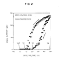
temperature (see Fig. 2).
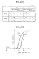
More specifically, referring to Fig. 2 of the
accompanying drawings, when the gate-source voltage is
swept vertically between a first voltage Vg0 (0 volt) and
a second voltage Vg1 (50 volts), the drain current of the
polycrystalline silicon element exhibits hysteresis
characteristic. This phenomenon has not heretofore been
known at all but discovered experimentally first by the
inventors of the present application. The reason why
such hysteresis characteristic can make appearance will
be explained below.
Fig. 4A shows a band profile in a channel
region of a semiconductor device shown in Figs. 1A - 1D
in the state where the gate-source voltage Vgs is zero
volt. A drain current flows in the direction perpendicular
to the plane of the drawing. For convenience of
discussion, it is assumed in the following description
that the drain-source voltage is sufficiently low when
compared with the gate voltage, being however understood
that the observation mentioned below applies equally
valid even in the case where the drain-source voltage is
high.
Now referring to Fig. 4A, there is formed in a
channel (3) of polycrystalline silicon a potential well
of low energy between a gate oxide film (5) and a peripheral
SiO2-protection film (10). In this case, energy
level (11) of a conduction band in the channel region
(3) which may be of p-type or of i-type (intrinsic
semiconductor type) or n-type with a low impurity
concentration is sufficiently high when compared with
energy level of a conduction band in a n-type source
region of a high impurity concentration or Fermi level
(12) in a degenerate n-type source region of a high
impurity concentration. As a consequence, there exist
no electrons within the channel (3). Thus, no drain
current can flow.
Further, a trap level (7) exists in the
vicinity of the channel (3), which can capture or trap
carriers such as electrons. As levels which partake in
forming the trap level, there are conceivable a level
extending to a grain or a level of group of grains
(crystal grains in the channel regions of polycrystalline
silicon) themselves which are surrounded by a high
barrier, level internally of the grain, level at a
Si-SiO2 interface (i.e., interface between the channel
region (3) and the gate oxide film (5)), level inside
the gate oxide film (5) and others. However, it is of
no concern which of these levels forms the trap level.
Parenthetically, even after the experiments conducted by
the inverters, it can not be ascertained at present by
which of the aforementioned levels the carriers or
electrons are trapped in actuality. Of the levels
mentioned above, energy in the trap level (7) which
plays a role in realizing the hysteresis characteristic
mentioned above is sufficiently higher than the Fermi
level (12) in the source region (1). Accordingly, no
electrons exist in the trap level (7). At this
juncture, it should be added that although the trap
level is shown in Figs. 4A - 4C as existing within the
gate oxide film, the trap level need not exist
internally of the oxide film. It is only necessary that
the trap level exists in the vicinity of the channel.
As the potential difference Vgs between the
gate (4) and the source (1) is increased from zero volt
to the low threshold voltage Vℓ, potential in the channel
region (3) increases. Consequently, as compared
with the initial energy level of the channel region (3)
in the state where the potential difference Vgs is zero
(refer to Fig. 4A), the potential of the channel region
(3) for electrons becomes lower under the condition that
the potential difference Vgs is higher than zero volt and
lower than the low threshold voltage Vℓ. When the gate-source
potential difference Vgs has attained the low
threshold voltage Vℓ, the Fermi level in the source
region (1) approaches to the energy level in the conduction
band of the channel region (3) (with a difference
of about kT, where k represents Boltzmann's constant and
T represents operating temperature in Kelvin). Consequently,
electrons are introduced into the channel region
(3) from the source. Thus, a current flow takes place
between the drain and the source.
When the gate voltage is further increased,
the number of electrons within the channel region (3)
increases correspondingly. However, when the potential
difference Vgs has reached a capture voltage Vg1, energy
of the trap level (7) approaches to the Fermi level
(12), whereby at least one electron is entrapped or
captured by the trap level (7) because of distribution
of electrons under the influence of thermal energy of
those electrons which are introduced from the source
region (1). At that time, since the level of the trap
(7) is sufficiently lower than potentials of the gate
oxide (5) and peripheral SiO2-protection film (10), the
electron captured by the trap level (7) is inhibited
from migration to the gate oxide film (5) and the
peripheral SiO2-protection film due to thermal energy of
electron. Besides, because a grain boundary of high
energy of the polycrystalline silicon channel region (3)
exists in the vicinity of the trap level (7), for example,
at the Si-SiO2 interface, the electron captured by
the trap level (7) can not move from the trap level
(refer to Fig. 4C). However, since the other electrons
can move, the drain current continues to flow.
In this way, once a single electron is entrapped
or captured by the trap level (7), the threshold
voltage of the polycrystalline silicon semiconductor
element shown in Figs. 1A - 1D changes from the low
threshold voltage Vℓ to the high threshold voltage Vh,
the reason for which will be explained below.
When the gate-source potential difference Vgs
is lowered from the state shown in Fig. 4C within the
range of Vh < Vgs < Vg1, the number of electrons within
the channel region (3) is decreased. However, in
general, a high energy region exists in the periphery of
the trap level (7). Accordingly, the electron captured
by the trap level (7) remains as it is (refer to
Fig. 5A).
When the gate voltage is further lowered to a
value at which the potential difference Vgs attains the
high threshold voltage Vh, the Fermi level (12) of the
source region (1) becomes different from the energy
level of the conduction band of the channel (3) by
ca. kT, as a result of which substantially all of the
electrons within the channel disappear (see Fig. 5B).
Consequently, the drain current can flow no more.
However, the threshold voltage Vh at which no drain
current flow becomes higher than the low threshold
voltage Vℓ by a voltage corresponding to the charge of
electron captured in the trap level (7).
Further, by lowering the gate-source potential
difference Vgs to a value where the potential difference
Vgs becomes equal to zero, potential in the peripheral
high-energy region of the trap level (7) becomes lower
in accompanying the lowering of the gate voltage, which
results in that the electron captured by the trap level
(7) is released to the region of low energy through
tunneling under the effect of the electric field (refer
to Fig. 5C).
Subsequently, the gate-source potential difference
Vgs is again increased for the vertical sweeping.
By repeating this operation, hysteresis can be observed
in the drain current-versus-gate voltage characteristic
owing to trapping and release of the electron.
In this conjunction, the inventors have
discovered that the hysteresis characteristic mentioned
above appears only when the capacitance between the gate
and the channel is small. Incidentally, the experiment
conducted by the inventors shows that although a semiconductor
element having a gate length and a gate width
each of 0.1 micron can exhibit the aforementioned
hysteresis characteristic, a semiconductor element whose
gate length and gate width are on the order of 1 (one)
micron is incapable of exhibiting such hysteresis
characteristic.
Thus, it must be emphasized that smallness of
the capacitance Cgc between the gate electrode and the
channel region is indispensable for the aforementioned
hysteresis characteristic to make appearance, the reason
for which may be explained as follows. There exists
between an amount of charge Qs stored in the trap level
and a change ΔVt (= Vh - Vℓ) in the threshold value or
voltage the following relation:
ΔVt = Qs/Cgc
where Cgc represents capacitance between the gate and an
effective channel. With the phrase "effective channel",
it is intended to mean a region of the channel which
restrictively regulates magnitude of a current flowing
therethrough and which corresponds to a region of
highest potential energy in the current path. Thus,
this region may also be termed a bottle-neck region. In
order to make use of the aforementioned hysteresis
characteristic as the memory function, it is necessary
that the state in which the threshold value is high (Vh)
and the state where the threshold value is low (Vℓ) can
definitely and discriminatively be detected as a change
in the drain current. In other words, difference
between the threshold values Vh and Vℓ has to be clearly
or definitely sensed in terms of a difference or change
appearing in the drain current. The conditions to this
end can be determined in the manner described below. In
general, the drain current Id of a MOS transistor having
a threshold value Vt can be represented in the vicinity
of the threshold value by the following expression:
Id = A•exp[q(Vgs - Vt)/(kT)]
where A represents a proportional constant, q represents
charge of an electron, Vgs represents a gate-source
voltage of the MOS transistor, Vt represents the
threshold voltage, k represents Boltzmann's constant and
T represents an operating temperature in degree Kelvin.
Thus, when Vt = Vh, the drain current is given by
Idh = A•exp[q(Vgs - Vh)/(kT)]
while when Vt = Vℓ, the drain current is given by
Idℓ = A•exp[q(Vgs - Vℓ)/(kT)]
Thus, ratio between the drain currents in the state
where Vt = Vh and the state Vt = Vℓ can be determined as
follows:
Idℓ/Idh = exp[q(Vh - Vℓ)/(kT)]
Thus, it can be appreciated that in order to
make it possible to discriminate the two states
mentioned above from each other on the basis of the
drain currents as sensed, it is necessary that the drain
current ratio Idℓ/Idh as given by the expression (5) is
not smaller than the base e (2.7) of natural logarithm
at minimum, and for the practical purpose, the current
ratio of concern should preferably be greater than "10"
(ten) inclusive. On the condition that the drain
current ratio is not smaller than the base e of natural
logarithm, the following expression holds true.
ΔVt( = Vh - Vℓ) > kT/q
Thus, from the expression (1), the following condition
has to be satisfied.
Qs/Cgc > kT/q
In order that the capture of a single electron
can meet the current sense condition mentioned above, it
is then required that the following condition be
satisfied.
q/Cgc > kT/q
From the above expression (8), it is apparent
that in order to enable operation at a room temperature,
the gate-channel capacitance Cgc should not exceed 6 aF
(where a is an abbreviation of "atto-" meaning 10-18).
Incidentally, in the case of the semiconductor element
having the gate length on the order of 1 micron, the
gate-channel capacitance Cgc will amount to about 1 fF
(where f is an abbreviation of "femto-" meaning 10-15)
and deviate considerably from the above-mentioned
condition. By contrast, in the case of a semiconductor
element fabricated by incarnating the teaching of the
invention, the gate-channel capacitance Cgc is as
extremely small as on the order of 0.01 aF, and it has
thus been ascertained that a shift in the threshold
value which can be sensed is brought about by the
capture of only a single even electron at a room
temperature.
Further, in the course of the experiment, the
inventors have found that by holding the gate-source
potential difference Vgs between zero volt and the
voltage level Vg1, the immediately preceding threshold
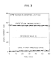
value can be held stably over one hour or more. Fig. 3
of the accompanying drawing shows the result of this
experiment. More specifically, Fig. 3 illustrates
changes in the drain current as measured under the
condition indicated by a in Fig. 2 while holding the
gate voltage to be constant. As can be seen in the
figure, in the state of low threshold value, a high
current level can be held, while in the state of high
threshold value, a low current level can be held. Thus,
by making use of the shift of the threshold value, it is
possible to hold information or data, i.e., to store
information or data, to say in another way. Further, by
sensing the drain current in these states, it is possible
to read out the data. Namely, the state in which
the drain current is smaller than a reference value 13
may be read out as logic "1" data, while the state in
which the drain current is greater than the reference
value (13) may be read out as logic "0" (refer to
Fig. 3).
On the other hand, data write operation can be
effectuated by controlling the gate voltage. Now,
description will be directed to the data write operation.
It is assumed that in the initial state, the gate
voltage is at the low level Vg0. By sweeping the gate
voltage in the positive direction to the level Vg1 the
threshold voltage at is set the high level Vh. With
this operation, logic "1" of digital data can be written
in the semiconductor element according to the invention.
Subsequently, the gate voltage is swept in the negative
direction to the zero volt level to thereby change the
threshold voltage to the low level Vℓ. In this way,
logic "0" of digital data can be written.
As will now be understood from the foregoing
description, it is possible to write, hold and read the
data or information only with a single semiconductor
element. This means that a memory device can be
implemented with a significantly smaller number of
semiconductor elements per unit area when compared with
the conventional memory device.
The semiconductor element according to the
invention in which data storage is realized by capturing
or entrapping only a few electrons in a storage node
(which may also be referred to as the carrier confinement
region or level node or carrier trap or carrier
confinement trap, quantum confinement region or the like
terms) can enjoy an advantage that no restriction is
imposed on the number of times the data can be rewritten
due to deterioration of the insulation film as encountered
in a floating-gate MOSFET or restriction, if
imposed, is relatively gentle.
It is however noted that in the case of the
mode illustrated in Figs. 1A - 1D for carrying out the
invention, relative positional relationship (i.e.,
relative distance) between the carrier trap level
serving for the carrier confinement and the effective
channel region serving as the current path is rather
difficult to fix, involving non-ignorable dispersions of
the threshold value change characteristic among the
elements as fabricated.
As one of the measures for coping with the
difficulty mentioned above, there is proposed another
mode for carrying out the invention such as one illustrated
in Figs. 10A and 10B of the accompanying drawings
in which the carrier confinement region (24) surrounded
by a potential barrier is provided independently in the
vicinity of a channel region (21). With this structure,
the dispersion mentioned above can be reduced.
From the stand point of performance stability
of the semiconductor element, it is preferred that
dispersion of the voltage difference ΔVt between the
high threshold voltage Vh and the low threshold voltage
Vℓ among the semiconductor elements as fabricated should
be suppressed to a possible minimum.
Certainly, the condition given by the expression
(1) can apply valid when the capacitance Cgt between
the gate region and the carrier confinement region as
well as the capacitance C between the carrier confinement
region and the channel region is sufficiently
small. In the other cases than the above, the condition
given by the following expression applies valid:
ΔVt = q/(1 + Cgt/C)Cgc
where Cgc represents capacitance between the gate region
(22) and the channel region (21), Cgt represents
capacitance between the carrier confinement region (24)
and the channel (21).
In conjunction with the mode shown in Figs. 1A
- 1D for carrying out the invention, the inventors have
found that the term C representing the capacitance
between the carrier confinement region and the channel
region in the expression (9) is most susceptible to the
dispersion because the carrier confinement region is so
implemented as to assume the carrier trap level. In
order that the potential difference ΔVt mentioned above
scarcely undergoes variation notwithstanding of
variation in the capacitance C between the carrier
confinement region and the channel region, the
capacitance Cgt between the gate electrode and the
channel region must be sufficiently smaller than the
capacitance C (i.e., Cgt < C).
Thus, according to another preferred mode for
carrying out the invention, it is proposed to set at a
small value the capacitance Cgt between the gate electrode
(22) and the carrier confinement region (24) by
interposing a gate insulation film (23) of a great
thickness while setting at a large value the capacitance
C between the carrier confinement region (24) and the
channel region (21) by interposing therebetween an
insulation film (25) of a small thickness.
On the other hand, in conjunction with the
holding of data in the carrier confinement region (24),
it is necessary to ensure stability against thermal
fluctuations. At this juncture, let's represent by Ctt
the total capacitance existing between the carrier
confinement region and all the other regions. In
general, in the absolute temperature (T) system, energy
fluctuation on the order of kT (where k represents
Boltzmann's constant and T represents temperature in
degree Kelvin) will be unavoidable. Accordingly, in
order to hold the data stably, it is required that
change of energy given by q2/2Ctt as brought about by
capturing a single electron is greater than the fluctuation
mentioned above. To say in another way, the
condition given by the following expression will have to
be satisfied.
q2/2Ctt > kT
This condition requires that the total capacitance
Ctt defined above has to be smaller than 3 aF
inclusive in order to permit operation at a room temperature.
In still another mode for carrying out the
invention as illustrated in Figs. 17A and 17B of the
accompanying drawings, a thin semiconductor film
structure (48) is formed interiorly of an insulation
film (49, 50) which is interposed between the storage
region (47) and the channel region (46) with a view to
reducing deterioration of the insulation film (49, 50).
Thus, in the semiconductor element implemented
in accordance with the instant mode for carrying out the
invention, a potential barrier provided by the thin film
structure (48) is formed interiorly of the insulation
film (49, 50) so that the thin film structure (48) plays
effectively a same role as the insulation film, while
making it possible to decrease the thickness of the
insulation film in practical applications.
As can be seen in Figs. 17A and 17B, the
semiconductor thin film (48) provided internally of the
insulation film (49, 50) has an energy level shifted by
the conduction band under the effect of the quantum
confinement effect in the direction thicknesswise of the
semiconductor thin film and serves essentially as a
potential barrier between the storage region and a
carrier supply region for the write/erase operations,
the reason of which will be elucidated below.
Representing the film thickness of the semiconductor
thin film by L, effective mass of the carrier
in the thin film by n and Planck's constant by h, energy
in the lowest energy state in quantum fluctuation of the
carrier due to the confinement effect in the thicknesswise
direction can appropriately be given by the following
expression:
h2/8mL2
In order that the energy shift due to the
quantum confinement effect is made effective in
consideration of the thermal energy fluctuation, the
condition given by the following inequality expression
(12) is required to be satisfied.
h2/8mL2 > kT
In the light of the above expression (12), the
thickness of the semiconductor thin film (48) formed of
silicon (Si) will have to be smaller than 9 nm inclusive
in order that the barrier is effective at a room
temperature.
Thus, although there is a probability of the
carrier existing in the semiconductor thin film for a
short time upon moving of the carriers between the
channel region (46) and the carrier confinement region
(47) via the insulation film (49, 50), the probability
of the carriers staying in the semiconductor thin film
(48) for a long time is extremely low. As a result of
this, the semiconductor thin film (48) operates as a
temporary passage for the carriers upon migration
thereof between the channel region (46) and the carrier
confinement region (47), which means that the semiconductor
thin film (48) will eventually serve as the
potential barrier because of incapability of the carrier
confining operation.
With the structure described above, the
semiconductor element can exhibit the barrier effect
with the insulation film of a smaller thickness when
compared with the semiconductor element in which the
above structure is not adopted. Thus, film fatigue of
the insulation film (49, 50) can be suppressed. For
further mitigating the film fatigue, the semiconductor
thin film (48) may be formed in a multi-layer structure.
The structure in which the semiconductor thin
film is provided in the insulation film can enjoy a
further advantage that the height of the potential
barrier between the carrier confinement region and the
source region can properly be set. Since the energy
shift due to the quantum confinement is determined in
accordance with the size L of the carrier confinement
region, it is possible to adjust the height of the
barrier by adjusting the film thickness in addition to
the selection of the thin film material. In this
connection, it should be noted that in the semiconductor
element of the structure known heretofore, the height of
the barrier is determined only on the basis of the
material constituting the insulation film.
The above other objects, features and
attendant advantages of the present invention will more
clearly be understood by reading the following description
of the preferred embodiments thereof taken, only by
way of example, in conjunction with the drawings.
BRIEF DESCRIPTION OF THE DRAWINGS
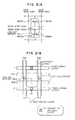
Figs. 1A to 1D are views for illustrating a
structure of a memory element according to a first
embodiment of the invention, wherein Fig. 1A is a top
plan view, Fig. 1B is microphotographic view of a
channel portion of the same Fig. 1C is a schematic
perspective view illustrating an overall structure of
the memory element, and Fig. 1D is a sectional view of
the same taken along a line C-C' in Fig. 1C;
Fig. 2 is a view showing graphically measured
values representing a gate-source voltage dependency of
a drain current of the memory element according to the
first embodiment of the invention;
Fig. 3 is a view showing experimentally
obtained results for illustrating holding of data by the
semiconductor element according to the first embodiment
after writing of logic "1" and "0";
Figs. 4A to 4C are views for illustrating
changes of a band profile in the vicinity of a channel
region of the semiconductor element according to the
first embodiment of the invention when gate voltage is
increased;
Figs. 5A to 5C are views for illustrating
changes of a band profile in the vicinity of a channel
region of the semiconductor element according to the
first embodiment of the invention when gate voltage is
lowered;
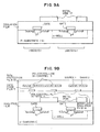
Fig. 6 is a schematic circuit diagram showing
a structure of a memory IC device according to the
invention in which the memory elements each having the
structure shown in Fig. 1 are employed;
Fig. 7 shows a hysteresis characteristic
expected to be exhibited by the memory device shown in
Fig. 6;
Fig. 8 is an exploded perspective view showing
schematically a structure of a semiconductor memory
device according to the first embodiment of the invention
in which a memory cell array is formed as stacked
on peripheral circuits formed in a Si-substrate surface;
Figs. 9A and 9B are sectional views for
illustrating fabrication steps of a semiconductor memory
device according to the first embodiment of the
invention;
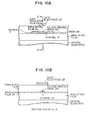
Figs. 10A and 10B are sectional views showing
a structure of a semiconductor memory element according
to a second embodiment of the invention;
Figs. 11A and 11B are enlarged views showing
exaggeratedly a channel region, a carrier confinement
region and a gate electrode of the memory element
according to the second embodiment of the invention,
wherein Fig. 11A is a perspective view and Fig. 11B is a
sectional view;
Fig. 12 is a view for illustrating graphically
a gate-source voltage dependency of a drain current in
the semiconductor memory element according to the second
embodiment of the invention;
Figs. 13A to 13C are schematic diagrams for
illustrating exaggeratedly changes in potential
distribution in the vicinity of a channel region and
carrier confinement region of a semiconductor memory
element when a gate voltage is increased;
Figs. 14A to 14C are schematic diagrams for
illustrating exaggeratedly changes in potential
distribution in the vicinity of a channel region and
carrier confinement region of a semiconductor memory
element when a gate voltage is lowered;
Figs. 15A and 15B are sectional views showing
a structure of a semiconductor memory element according
to a third embodiment of the invention;
Figs. 16A to 16C are views showing a structure
of a semiconductor memory element according to a fourth
embodiment of the invention, wherein Fig. 16A is a
sectional view, Fig. 16B shows a section taken along a
line a-a' in Fig. 16A and Fig. 16C is a top plan view;
Figs. 17A and 17B are views for illustrating a
semiconductor memory element according to a fifth
embodiment of the present invention wherein Fig. 17A is
a sectional view of the same and Fig. 17B shows a
potential distribution profile in the memory element;
Fig. 18 is a view showing a symbol representing
a semiconductor memory element according to the
invention;
Figs. 18A, 18B and 18C are views for illustrating
a memory cell according to a sixth embodiment of
the invention, wherein Fig. 18A shows a circuit configuration
of the memory cell, Fig. 18B shows voltages
applied to a word wire and a data wire of the memory
cell upon read and write operations, respectively, and
Fig. 18C is a view for graphically illustrating
dependency of a drain current on a gate-source voltage
of a semiconductor element employed in the memory cell;
Fig. 19 is a circuit diagram showing circuit
configuration of a read circuit for the memory cell
according to the sixth embodiment of the invention;
Fig. 20 is a signal waveform diagram for
illustrating timings at which various signals are
applied upon read operation;
Figs. 21A and 21B are diagrams showing a
circuit configuration of a 4-bit memory cell array
according to the sixth embodiment and a layout thereof,
respectively;
Figs. 22A to 22C are views showing a memory
cell set according to a seventh embodiment of the
invention, wherein Fig. 22A shows a circuit configuration
of the cell set, Fig. 22B shows voltages applied to
a memory element thereof upon write and read operations,
and Fig. 22C graphically illustrates characteristic of
the memory element;
Fig. 23 is a circuit diagram showing a
structure of a semiconductor memory device according to
the seventh embodiment of the invention;
Figs. 24A to 24E are circuit diagrams showing
various configurations of the memory cell according to
the invention;
Figs. 25A to 25C are views for illustrating a
memory cell according to an eighth embodiment of the
invention, wherein Fig. 25A shows a circuit configuration
of the memory cell, Fig. 25B shows voltages applied
to a word wire and a data wire of the memory cell upon
read and write operations, respectively, and Fig. 25C is
a view for graphically illustrating dependency of a
drain current on a gate-source voltage of a semiconductor
element employed in the memory cell;
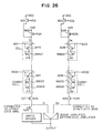
Fig. 26 is a circuit diagram showing circuit
configuration of a read circuit for the memory cell
according to the eighth embodiment of the invention;
Figs. 27A and 27B are circuit diagrams showing
versions of the memory cell circuit according to the
eighth embodiment, respectively;
Figs. 28A and 28B are a circuit diagram
showing a configuration of a four-bit memory cell and a
corresponding mask layout of the same, respectively;
Figs. 29A to 29C are views for illustrating a
memory cell according to a ninth embodiment of the
invention, wherein Fig. 29A shows a circuit configuration
of the memory cell, Fig. 29B shows voltages applied
to a word wire and a data wire of the memory cell upon
read and write operations, respectively, and Fig. 29C is
a view for graphically illustrating dependency of a
drain current on a gate-source voltage of a semiconductor
element employed in the memory cell;
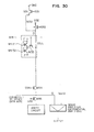
Fig. 30 is a circuit diagram showing a
read/write circuit according to the ninth embodiment of
the invention;
Figs. 31A, 31B and 31C are views for illustrating
a memory cell according to a tenth embodiment of
the invention, wherein Fig. 31A shows a circuit configuration
of the memory cell, Fig. 31B shows voltages
applied to a word wire and a data wire of the memory
cell upon read and write operations, respectively, and
Fig. 31C is a view for graphically illustrating
dependency of a drain current on a gate-source voltage
of a semiconductor element employed in the memory cell;
Fig. 32 is a circuit diagram showing a read
circuit according to the tenth embodiment of the
invention;
Fig. 33 is a view showing a version of a
memory cell according to the tenth embodiment; and
Fig. 34 is a block diagram showing a structure
of a data processing apparatus in which a memory device
according to the invention be employed as a main memory.
DESCRIPTION OF THE PREFERRED EMBODIMENTS
Now, the present invention will be described
in detail in conjunction with the preferred or exemplary
embodiments thereof by reference to the drawings.
Embodiment 1
Description which follows is directed to a
field effect semiconductor memory element (FET memory
element) according to an exemplary embodiment of the
present invention. Figs. 1A to 1D are views for
illustrating a structure of a semiconductor memory
element according to a first embodiment of the invention,
wherein Fig. 1C is a schematic perspective view
illustrating an overall structure of the memory element,
Fig. 1D is a sectional view of the same taken along the
line C-C' in Fig. 1C, Fig. 1B is an enlarged microphotographic
view showing a channel portion of the same, and
Fig. 1A is a top plan view thereof. Referring to the
figures, a source 1 and a drain 2 are each constituted
by a region formed of n-type polycrystalline silicon and
having a high impurity concentration while a channel
portion 3 is constituted by a region formed of a non-doped
polycrystalline silicon region. Each of the
source 1, the drain 2 and the channel 3 is realized in
the form of a thin and fine wire of polycrystalline
silicon. In the case of a memory device manufactured
actually by the inventors of the present application,
the channel 3 is 0.1 µm in width and 10 nm, preferably
3.4 nm in thickness. Connected to the ends of the
source 1 and the drain 2 are contacts 1A and 2A of polycrystalline
silicon, respectively, each of which has a
thickness greater than that of the source 1 and the
drain 2, wherein the source 1 and the drain 2 are
connected to metallic wiring conductors via the polycrystalline
silicon contacts 1A and 2A, respectively.
In the case of a typical example of the memory element,
each of the polycrystalline silicon contacts 1A and 2A
should preferably be implemented with a thickness of
0.1 µm which is ten times as large as that of the
channel 3, because, if otherwise, polycrystalline
silicon itself becomes insusceptible to etching upon
forming contact holes directly in thin polycrystalline
silicon. A gate electrode 4 is provided in such orientation
as to intersect the channel region 3 through an
interposed gate insulation film 5. In the case of the
instant embodiment, the film thickness of the gate
electrode 4 is 0.1 µm. The structure mentioned above
can best be seen from Fig. 1C.
Parenthetically, the polycrystalline silicon
film constituting the channel region 3 is wholly
enclosed by a SiO2-protection film 10 in the case of the
instant embodiment (see Fig. 1D). Because the dielectric
constant of silicon oxide (SiO2) is about one third
of that of silicon, capacitances of the channel region 3
and the gate electrode 4 can be reduced by enclosing
them with the SiO2-protection film 10 as mentioned
above. This is one of the reasons why the hysteresis
characteristic elucidated hereinbefore can be realized
at a room temperature.
In the case of the memory element according to
the instant embodiment, the channel of polycrystalline
silicon is formed by depositing amorphous silicon (a-Si)
in a thickness of 10 nm on a SiO2-substrate and crystallizing
by heat treatment at a temperature of 750°C. In
this conjunction, it has been found that the thickness
of amorphous silicon (a-Si) should preferably be in the
order of 3.5 nm. A structure of a channel portion is
shown in Fig. 1B. In the course of the heat treatment,
silicon crystal grains in amorphous silicon grow
progressively. However, when the size of the grain
reaches the film thickness, any further growth in the
direction perpendicular to the plane of the film is
prevented. At the same time, the rate of the grain
growth in the direction parallel to the film becomes
retarded. As a consequence, the grain size in the
lateral direction (i.e., in the direction parallel to
the film surface) is substantially equal to the film
thickness. For these reasons, the field-effect
semiconductor memory element according to the instant
embodiment of the invention features that the grain size
of polycrystalline silicon forming the channel region is
extremely small.
The small grain size mentioned above contributes
to realization of small capacitance between the
gate electrode and the channel region, the reason for
which will be elucidated below. In the field effect
element now under consideration, it is only a few
current paths 6 having lowest resistance in the channel
region 3 that a current can actually flow within a low-current
range close to a threshold level (see Fig. 1A).
To say in more concrete, the current flow takes place
due to migration or transfer of electrons from one to
another crystals grain. In the case of the instant
embodiment, the current path is extremely fine or thin
because of a very small grain size as mentioned above.
Consequently, the region in which electrons exists is
remarkably small when compared with whole the channel
region. For this reason, the capacitance Cgc which is
effective between the gate electrode and the effective
channel portion (in the sense defined hereinbefore) is
significantly small.
In the case of a semiconductor memory element
actually fabricated according to the instant embodiment,
the gate-channel capacitance Cgc mentioned above was set
at an extremely small value, e.g. 0.02 aF (atto-Farad),
with a view to observing the effect of change in the
threshold value to a possible maximum extent. As a
result of this, the range of voltages required for
operation expanded to several ten volts. Of course, by
setting the gate-channel capacitance Cgc at a greater
value, e.g. 0.2 aF, the operation voltage range can be
set to a range of several volts usually employed in the
conventional integrated circuit. To this end, the
thickness of the gate insulation film 5 may be decreased
and/or the length or width of the gate electrode may be
increased, which can be realized without any appreciable
technical difficulty.
In the case of the instant embodiment of the
invention, the channel is formed of polycrystalline
silicon. At this juncture, it should however be
mentioned that the hysteresis characteristic can be
realized even in a conventional bulk MOSFET formed in a
crystal silicon substrate if the gate-channel capacitance
mentioned above can be made so small that the
conditions mentioned previously can be satisfied. In
that case, the bulk MOSFET can be made use of as a
memory element. In this conjunction, it is however
noted that in the case of a bulk MOSFET, the effects of
the grain mentioned above are absent. Besides, the
lower side of the bulk MOSFET is covered with a Si-film
having a high dielectric constant. Consequently, it is
necessary to decrease the size of the bulk MOSFET element
when compared with the element having the channel
formed of polycrystalline silicon. This in turn means
that difficulty will be aggravated in manufacturing the
bulk MOSFET memory element. However, because the bulk
MOSFET has a greater mobility of carriers, it can handle
a large current and is suited for a high-speed operation,
to an advantage. As a further version, the
hysteresis characteristic mentioned previously can be
realized by using a MOSFET of SOI (Silicon-On-Insulator)
structure as well. The SOI structure can be implemented
by growing monocrystalline silicon on an insulation film
and by forming a MOSFET therein. Because the gate-channel
capacitance of the SOI MOSFET can be made
smaller than that of the bulk MOSFET, the hysteresis
characteristic can be realized with a greater size when
compared With the bulk MOSFET.
The foregoing description has been made on the
assumption that the channel for migration of electrons
is of n-type. It should however be mentioned that
similar operation can be accomplished by using holes.
Further, other semiconductor material than silicon can
be employed in forming the channel region.
Additionally, it has been assumed in the
foregoing description that the gate electrode 4 is
located beneath the channel region 3. However, similar
operation can be effectuated equally with such structure
in which the gate electrode lies above the channel
region. Besides, gate electrodes may be provided above
and beneath the channel, respectively, for realizing
similar operation and effects as those mentioned previously.
Furthermore, the gate electrode may be disposed
at a side laterally of the channel region. Moreover,
gate electrodes may be provided at both sides of the
channel, respectively.
Now, referring to Fig. 6, description will be
made of an integrated memory circuit which is comprised
of the semiconductor elements of the structure described
above. Fig. 6 shows a structure of a memory IC device
in which polycrystalline silicon memory elements each
having the structure shown in Fig. 1 are employed. In
this conjunction, it is assumed that each of the
semiconductor elements or the polycrystalline silicon
memory elements has such hysteresis characteristic as
illustrated in Fig. 7. More specifically, it is
presumed that when a voltage Vw is applied between the
gate and the source, the memory element takes on logic
"1" state (state of high threshold value represented by
Vh) while upon application of a voltage of -Vw between
the gate and the source, the memory element assumes
logic "0" state (low threshold state Vℓ). On the other
hand, application of a voltage in a range of -Vw/2 to
Vw/2 between the gate and the source or between the gate
and the drain, the threshold voltage undergoes no
change. The characteristic illustrated in Fig. 7 is
comparable to that shown in Fig. 2 except that the
threshold value is lowered as a whole and can be
realized by introducing a donor impurity in the channel
region of the memory element upon manufacturing thereof.
Referring to Fig. 6, each of semiconductor
memory elements MP1 to MP4 is constituted by a semiconductor
element according to the invention which has the
structure shown in Fig. 1 and the hysteresis characteristic
illustrated in Fig. 7. Each of the semiconductor
memory elements has a gate terminal connected to a word
wire, a drain terminal connected to a data wire and a
source terminal connected to the ground potential.
Operation for writing digital data in the
integrated memory circuit is performed through cooperation
of a word wire driver circuit and a data wire
driver circuit shown in Fig. 6 in a manner described
below. For writing logic "1" in the memory element MP1,
the potential on the word wire 1 is set to a voltage
level of Vw/2 with the potential of the data wire 1
being set to -Vw/2, while the other word wires and data
wires are set to zero volt. As a result of this, a
voltage of Vw is applied between the gate and the drain
of the memory element MP1, which thus takes on the logic
"1" state (high threshold state). At this time point,
all the other memory elements than the memory element
MP1 are applied with a voltage not higher than Vw/2.
Accordingly, no change takes place in the threshold
voltage in these other memory elements. On the other
hand, for writing logic "0" in the memory element MP1,
the potential on the word wire 1 is set to -Vw/2 with
the potential on the data wire 1 being set to Vw/2.
Thus, the voltage of -Vw is applied between the gate and
the drain of the memory element MP1, whereby the memory
element MP1 is set to logic "0" state (low threshold
state Vℓ). At this time point, all the other memory
elements than the memory element MP1 are applied with a
voltage which is not higher than -Vw/2. Accordingly, no
change can take place in the threshold value in these
other memory elements.
On the other hand, reading of information or
data is carried out in a manner described below (see
Fig. 6). In the data wire driver circuit, the data wire
is connected to a voltage source via a load element. On
the other hand, the other end of the data wire is connected
to a sense amplifier. Now, operations involved
in reading out data from the memory element MP1 will be
considered. To this end, the potential of the word wire
1 as selected is set to the level of zero volt while the
potential on the other word wire 2 not selected is set
to the voltage level of -Vw/2. When the memory element
MP1 is in the logic "1" state, this means that the
memory element MP1 is in the off-state (i.e., nonconducting
state) with the data wire remaining in the
logically high state. Even when the memory element MP2
is in the logical "0" state, no current can flow through
the memory element MP1 because the word wire not select
is at the potential level of -Vw/2. When the memory
element MP1 is in the logic "0" state, a current flows
from the data wire 1 to the grounded wire via the memory
element MP1, resulting in lowering of the potential at
the data wire 1. This potential drop is amplified by
the sense amplifier, whereupon the data read-out
operation comes to an end. The memory device can be
implemented in this manner.
In the memory device now under consideration,
peripheral circuits thereof such as a decoder, the sense
amplifier, an output circuit and the like are implemented
by using the conventional bulk MOSFET formed in a
surface of a Si-substrate in such an arrangement as
illustrated in Fig. 8, and a memory cell array including
the memory elements MP1 to MP4 each of the structure
illustrated in Fig. 1 are fabricated on the peripheral
circuits with an interposition of an insulation film.
This is because polycrystalline silicon for the memory
elements MP1 to MP4 can be fabricated on the bulk
MOSFETs. By virtue of this structure, the space or area
otherwise required for the peripheral circuits can be
spared, whereby the memory device can be implemented
with about twice as high an integration density when
compared with that of the conventional dynamic RAM.
Parenthetically, it should be added that a wiring layer
which exists in actuality between the bulk MOSFETs and
the polycrystalline silicon transistor layer is omitted
from illustration in Fig. 8.
As will be appreciated from the foregoing
description, with the structure of the memory device
according to the instant embodiment of the invention,
there can be realized a integrated memory circuit with a
high integration density because of capability of
storing single-bit information by the single memory
element. Besides, the integration density can further
be increased by stacking the memory cell array on the
peripheral circuit layer in a laminated or stacked
structure. Additionally, there is no necessity for
reading out a quantity of electric charge, as required
in the case of the conventional dynamic RAM, but the
signal can be generated on the data wire in a static
manner, so to say. Owing to this feature, fine structurization
can further be enhanced without involving
degradation in the signal-to-noise ratio (S/N ratio).
Moreover, information as stored can be retained over an
extended time period, which means that refreshing operation
as required in the case of the dynamic RAM can be
rendered unnecessary. Consequently, power consumption
can be suppressed to a possible minimum. Further, the
peripheral circuits can be implemented in much simplified
configuration. Owing to the features mentioned
above, there can be realized according to the teachings
of the invention incarnated in the instant embodiment a
semiconductor memory device with an integration density
which is at least twice as high as that of the conventional
dynamic RAM while the cost per bit can be reduced
at least to a half of that required in the conventional
dynamic RAM. Of course, electric power required for
holding or retention of information (data) can significantly
be reduced.
In the foregoing description, it has been
assumed that the low threshold voltage Vℓ is of negative
polarity with the high threshold level Vh being positive,
as illustrated in Fig. 7. However, even when
these threshold voltages Vℓ and Vh for the memory element
are set at higher levels, respectively, similar operation
can be ensured simply by setting correspondingly
higher the gate control signal level.
Next, by reference to Figs. 9A and 9B,
description will turn to a process for fabricating or
manufacturing the memory element and the memory device
according to the instant embodiment of the invention.
At first, an n-channel MOS 15 and a p-channel MOS 16
(i.e., a CMOS (Complementary Metal-Oxide Semiconductor
device) are fabricated on a surface of a p-type Si-substrate
14, which is then followed by formation of an
insulation film over the CMOS device as well as formation
of metal wires 17 (refer to Fig. 9A). Subsequently,
an inter-layer insulation film 18 is deposited
and the surface thereof is flattened for reducing
roughness. Next, a polycrystalline silicon region which
is to serve as a gate electrode 4 of the memory element
is formed on the flat surface of the insulation layer
18. To this end, the polycrystalline silicon region is
doped with n-type impurity at a high concentration so
that it exhibits a low resistance. Next, a SiO2-film
which is to serve as a gate insulation film 5 is
deposited in thickness on the order of 50 nm over the
insulation layer 18 having the gate electrodes through a
chemical vapor deposition method (i.e., CVD method in
abbreviation), which is then followed by deposition of
an amorphous silicon layer. After patterning of the
amorphous silicon layer, source regions 1 and drain
regions 2 are doped with n-type impurity such as As, P
or the like through ion implantation and annealed at a
temperature of about 750°C, whereby channels 3 of polycrystalline
silicon are formed. Finally, a protection
or passivation film 10 of SiO2 is formed. Thus, there
can be fabricated a memory device of high integration
density according to the invention (refer to Fig. 9B).
At this juncture, it should be added that an electrically
conducting layer may be provided on the top surface
of the memory device for the purpose of shielding the
memory device against noise to thereby enhance the
reliability thereof.
Embodiment 2
Figs. 10A and 10B are sectional views showing
a memory element according to a second embodiment of the
invention. An SOI (Silicon-On-Insulator)-substrate is
employed as the substrate, wherein Fig. 10B shows a
section taken along as line a-a' in Fig. 10A. A source
region 19 and a drain region 20 are each constituted by
an n-type silicon region of high impurity concentration
and low resistance, wherein a channel 21 of silicon
extending between the source and drain regions 19 and 20
is formed in a fine or thin wire. A thin film 25 of
SiO2 is formed over the channel 21. Further, a storage
node 24 for confining carriers with silicon grains is
formed on the channel region 21. A gate electrode 22 is
provided above the channel region 21 with a gate insulation
film 23 being interposed therebetween.
With the structure of the memory element
according to the instant embodiment, the capacitance Cgc
between the channel region 21 and the gate electrode 22
can be reduced because of a very small wire width of the
channel 21. Writing and erasing operations can be
effected by changing potential level. More specifically,
the writing can be carried out by injecting electrons
from the channel region into the storage node 24
by clearing a potential barrier provided by the insulation
film 25, while for erasing the stored information,
electrons are drawn out from the storage node 24. Thus,
in the memory element according to the instant embodiment,
writing and erasure of or data information to and
from the storage node 24 are performed by transferring
the electrons with the channel. It should however be
mentioned that these operations can be realized through
electron transferring with other region than the channel
region. The same holds true in the embodiments of the
invention which will be described below. Further,
although silicon is employed for forming the source, the
drain and the channel with SiO2 being used for forming
the insulation films in the memory element according to
the instant embodiment, it should be understood that the
source and the drain may be formed of other semiconductor
material or metal and that the insulation film
may also be formed with other compositions so long as
the capacitance Cgc satisfying the requisite conditions
mentioned previously can be realized.
Additionally, it is important to note that
although the storage node 24 is provided above the
channel 21 in the memory element according to the
instant embodiment, the storage node 24 may be provided
beneath the channel region or at a location laterally of
the channel region. Besides, although it has been
described that the SOI substrate is employed with monocrystalline
silicon being used for forming the source,
the drain and the channel, it should be understood that
they may be formed by using polycrystalline silicon as
in the case of the first embodiment. In that case,
difference from the first embodiment can be seen in that
the storage node 24 is provided independently. It
should further be added that the material for the insulation
film interposed between the channel region and
the storage node need not be same as the material of the
insulation film interposed between the gate and the
storage node.
Although it is presumed that the carriers are
electrons in the memory element and the memory device
according to the instant embodiment, holes may equally
be employed as the carriers substantially to the same
effect. This holds true in the embodiments described
below as well.
According to the teachings of the invention
incarnated in the instant embodiment, the storage node
24 is formed by using crystal grains of a small size,
wherein the storage node 24 of Si-grains is surrounded
or enclosed by the gate insulation film 23 and the
insulation film 25 of SiO2 to thereby reduce surrounding
parasitic capacitance. Because of the small size of the
grains constituting the storage node 24, the surrounding
or total capacitance Ctt therefor may be determined in
terms of intrinsic capacitance. In the case of a
spherical body having a radius r and enclosed by a
material having a dielectric constant ε, the intrinsic
capacitance thereof is given by 4πεr. By way of example,
for the storage node formed by silicon crystal
grains having a grain size of 10 nm, the surrounding or
total capacitance Ctt of the storage node is about 1 aF.
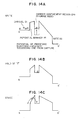
Figs. 11A and 11B show schematically and
exaggeratedly a channel region, a carrier confinement
node and a gate electrode in a perspective view and a
sectional view, respectively.
Referring to Fig. 12, when a gate-source
voltage (i.e., voltage applied between the gate and the
source) is swept between a first voltage Vg0 (zero volt)
and a second voltage Vg1 (5 volts) in the vertical direction
as viewed in Fig. 12, the drain current exhibits a
hysteresis characteristic. In this conjunction, relevant
potential distributions on and along a plane b-b'
in Fig. 11B are illustrated in Figs. 13A to 13C and
Figs. 14A to 14C. The reason why the hysteresis characteristic
such as illustrated in Fig. 12 makes appearance
will be elucidated below.
In the semiconductor memory element shown in
Fig. 10, potential distribution making appearance in the
channel region 21 when the potential difference Vgs
between the gate and the source is zero volt is schematically
shown in Fig. 13A. This corresponds to the state
25 shown in Fig. 12. Parenthetically, it is assumed
that the drain current flows in the direction perpendicular
to the plane of the drawing Fig. 13A. The
description which follows will be made on the assumption
that the drain-source voltage is sufficiently low as
compared with the gate voltage, being however understood
that the following description applies valid as it is,
even when the voltage between the drain and the source
is high.
Now referring to Fig. 13A, in the channel
region 21 surrounded by a potential barrier 25 formed
between the channel region 21 and the storage node 24
and the peripheral SiO2-film 23, there prevails a low-energy
potential. Thus, the storage node 24 (carrier
confinement region) formed of Si-grains and surrounded
by the insulation films 23 and 25 can capture or trap
the carriers or electrons. On the other hand, no
electrons exist in the channel region 21 because energy
level of the conduction band in the channel region 21 of
P-type or N-type having low impurity concentration or
i-type (intrinsic semiconductor type) is sufficiently
higher than the energy level of the conduction band in
the N-type source 19 of a high impurity concentration or
Fermi level in the N-type degenerate source region 19
having a high impurity concentration. Consequently, no
drain current can flow.
Incidentally, energy in the carrier confinement
region or the storage node 24 is sufficiently
higher than the Fermi level in the source region 19.
Thus, no electron exists in this region 24 either.
As the potential difference Vgs between the
gate electrode 22 and the source 19 is increased from
zero volt to the low threshold voltage Vℓ, potential in
the channel region 21 increases. As a consequence,
potential in the channel region 21 for electrons becomes
lower, as can be seen in Fig. 13B, hereby electrons are
introduced into the channel region 21 from the source
19. Thus, a current flow takes place between the source
and the drain.
When the gate voltage is further increased,
the number of electrons existing in the channel region
21 increases correspondingly. However, when the gate-source
voltage Vgs reaches a writing voltage Vg1, energy
in the storage node 24 becomes low, being accompanied
with a corresponding increase of the potential gradient
between the channel 21 and the storage node 24. As a
consequence of this, at least one electron will be
entrapped in the storage node 24 by clearing the potential
barrier 25 due to thermal energy distribution of
electron and/or tunneling phenomenon (tunnel effect).
This corresponds to transition from the state 27 to the
state 28, as illustrated in Fig. 12.
Thus, there takes place a Coulomb blockade
owing to one electron trapped in the storage node 24 as
well as potential increase, whereby injection of another
electron in the storage node 24 is prevented, as is
illustrated in Fig. 14A.
In this way, every time one electron is
entrapped in the storage node 24, the threshold voltage
of the semiconductor memory element shown in Fig. 10
changes from the low threshold Vℓ to the high threshold
voltage Vhs, the reason for which will be explained
below.
When the gate-source voltage Vgs is lowered
within the range of Vh (high threshold voltage) < Vgs <
Vℓ (low threshold voltage), starting from the state
illustrated in Fig. 14A, the number of electrons in the
channel region 21 decreases. However, electron captured
or trapped in the storage node 24 remains as it is,
because of existence of the potential barrier 25 between
the storage node 24 and the channel 21.
When the voltage of the gate electrode 22 is
lowered to a level where the potential difference Vgs is
equal to the high threshold voltage Vh, the Fermi level
in the source 19 becomes different from the energy level
of the conduction band in the channel 21 by a magnitude
on the order of kT, as a result of which substantially
all of the electrons in the channel region make disappearance,
(refer to Fig. 14B). This corresponds to the
state 29 shown in Fig. 12. At this juncture, it should
however be mentioned that the threshold value Vh at
which the drain current can no more flow becomes higher
than the low threshold voltage Vℓ by an amount of the
charge of the electrons captured in the storage node 24.
As the gate-source voltage Vgs is further
lowered to a level where it becomes equal to zero volt,
the potential gradient between the storage node 24 and
the channel region 21 becomes steeper correspondingly,
as a result of which the electron captured in the
storage node 24 is released owing to the tunneling
effect brought about by thermal energy distribution of
electrons and the field effect (refer to Fig. 14C).
Potential profile in the state where electrons are
dispelled is equivalent to the initial potential profile
illustrated in Fig. 13A. This means that the semiconductor
memory element resumes the state 25 shown in
Fig. 12.
Subsequently, when the gate-source voltage Vgs
is again increased for effecting repeatedly the sweep in
the vertical direction, hysteresis phenomenon which
accompanies the capture/release of electron can be
observed.
In the structure of the memory element now
under consideration, the condition given by the expression
(8) has to be satisfied in order to detect the
presence/absence of a single electron in terms of a
current.
Next, description will turn to a method of
fabricating the memory element or memory device according
to the instant embodiment of the invention. AS is
shown in Figs. 10A and 10B, the source region 19, the
drain region 20 and the channel region 21 are formed in
the SOI substrate by resorting to a photoetching
process. The channel region is realized in the form of
a fine or thin wire. The source and drain regions are
doped with n-type impurity at a high concentration. By
contrast, the channel region is doped with n-type or i-type
or p-type impurity at a low impurity concentration.
Subsequently, the SiO2-film 25 is deposited through a
CVD (chemical vapor deposition) process, which is then
followed by formation of a crystal silicon grain or the
storage node 24 through a CVD process.
In order to form the silicon crystal grain 24
(which is to serve as the storage node 24) having a very
small radius r, a nucleus formed initially in the CVD
deposition process is made use of for forming the
crystal silicon grain 24. To this end, formation of the
crystal silicon grain 24 by the CVD method should be
carried out at a low temperature and completed within a
short time.
Embodiment 3
Fig. 15A and 15B show in sections a memory
element according to a third embodiment of the present
invention, respectively, in which Fig. 15B is a sectional
view taken along a line a-a' in Fig. 15A. The
memory element or memory device according to the instant
embodiment differs from the second embodiment in that
the former is implemented in such a structure in which a
channel region 33 and a carrier confinement region or
storage node 34 are sandwiched between a pair of gate
electrodes 31 and 32. Thus, in the memory element or
memory device according to the instant embodiment,
writing and erasing operations can be performed not only
from the first gate electrode 31 but also through the
medium of the second gate electrode 32.
In the case of memory element or memory device
according to the second embodiment of the invention, it
is expected that potential profiles in the carrier
confinement region and in the vicinity of the channel
region inclusive thereof may undergo variation under the
influence of change in the external potential. By
contrast, the memory element or memory device according
to the instant embodiment is less susceptible to the
influence of such external potential change owing to the
shielding effect of the gate electrodes provided at both
sides, to an additional advantage.
Embodiment 4
Figs. 16A to 16C show a memory element
according to a fourth embodiment of the invention,
wherein Fig. 16A is a sectional view, Fig. 16B shows a
section taken along a line a-a' in Fig. 16A and Fig. 16C
is a top plan view. Referring to the figures, formed
over a channel region 39 of a bulk MOSFET in which a
source 35 and a drain 36 are formed in a silicon
semiconductor crystal substrate is an insulation film 40
on which a plurality of silicon crystal grains 41 are
formed. Further, an insulation film 42 is formed over
the insulation film 40 and the grains 41. Additionally,
a second gate electrode 38 is deposited on the insulation
film 42. This gate electrode 38 is of such a shape
that a gap exists in the direction interconnecting the
source 35 and the drain 36. A first gate electrode 37
is provided above the second gate electrode 38 with an
insulation film 43 being interposed therebetween. The
source 35 and the drain 36 are each constituted by a
region formed of an n-type bulk silicon having a high
impurity concentration, wherein a p-type region 44
intervenes between the source region 35 and the drain
36.
By applying a voltage of positive or plus
polarity to the first gate electrode 37, electrons are
induced in a surface portion of the p-type region 44,
whereby a channel 39 is formed. In that case, the
potential of the second gate electrode 38 is set lower
than the first gate electrode 37 so that the second gate
electrode 38 also operates as an electrostatic shield
electrode. As a result of this, the channel region 45
is formed only in a region located in opposition to the
fine gap of the second gate electrode 38, whereby the
effective capacitance Cgc between the first gate electrode
37 and the channel region 39 can be made smaller.
Writing and erasing operations can be realized by
changing the potential of the first gate electrode 37 or
the second gate electrode 38 or the substrate 37 in a
substantially same manner as described hereinbefore in
conjunction with the third embodiment.
Embodiment 5
Fig. 17A shows a cross section of a memory
element according to a fifth embodiment of the present
invention. The direction in which the current flows
extend perpendicularly to the plane of the drawing. The
channel region and the carrier confinement region (storage
node) as well as regions located in the vicinity are
shown exaggeratedly. The source and the drain are
implemented in same configurations as those of the
memory element according to the second embodiment of the
invention. The instant embodiment differs from the
second embodiment in that a thin film 48 of silicon is
formed in SiO2-insulation films 49 and 50 between a
channel region 46 of silicon and a storage node (carrier
confinement node) 47 formed by a silicon crystal grain.
Carriers within a channel 46 can reach the
storage node (carrier confinement region) 47 via the
Si-thin film 48. Fig. 17B shows a potential profile in
the memory element of the structure mentioned above.
Referring to Fig. 17B, an energy shift 52 takes place in
the Si-thin film 48 due to the quantum confinement
effect in the direction thicknesswise. The thin Si-film
48 plays a role as a barrier for the migration of
electron from the Si-channel region 46 to the carrier
confinement region (storage node) 47. As a result of
this, for achieving the same barrier effect, the sum of
film thicknesses of the SiO2-films 49 and 50 existing
between the channel and the carrier confinement region
may be reduced as compared with the film thickness of
the SiO2-film located between the channel region and the
carrier confinement region of the memory element in
which the structure according to the instant embodiment
is adopted (e.g. refer to Figs. 10A and 10B). Accordingly,
fatigue of the insulation film can be mitigated,
whereby the number of the times the memory is rewritten
can be increased.
It should further be mentioned that the
potential barrier realized by making use of the quantum
confinement effect described above is effective for
protecting the insulation film against fatigue even in
the case where a greater number of carriers are to be
handled by the carrier confinement region.
Embodiment 6
A structure of a memory read circuit for a
semiconductor memory device according to the invention
will be described by reference to Figs. 18A to 18C and
Fig. 19. In the description which follows, the semiconductor
memory element according to the invention
which may be one of the elements described hereinbefore
by reference to Figs. 1A - 1D, Fig. 6, Figs. 10A, 10B,
Figs. 15A, 15B, Figs. 16A - 16C and Figs. 17A, 17B,
respectively, is identified by representing the carrier
trapping node (carrier confinement region) by a solid
circle as shown in Fig. 18 for the purpose of discrimination
from the conventional field effect transistor.
On Figs. 18A to 18C, Fig. 18A shows a circuit configuration
of a single-bit memory cell, Fig. 18B shows
voltages applied to a word wire W and a data wire D upon
read and write operations, respectively, and Fig. 18C
graphically illustrates a dependency of a drain current
on a gate voltage (gate-source voltage) in a semiconductor
element MM7 employed for realizing the memory
cell. The circuit configuration per se is identical
with that described hereinbefore in conjunction with the
first embodiment by reference to Fig. 6.
Fig. 19 shows a circuit configuration for
reading data or information stored in a memory cell MM1.
Needless to say, a large number of memory cells similar
to the memory cell MM1 are disposed in an array in the
memory device which the invention concerns, although
illustration thereof is omitted. The memory cell MM1
serving for storing information differs from the
conventional MOSFET known heretofore in that the value
of a current which can be handled by the memory cell is
smaller as compared with that of the MOSFET. This is
because the gate-channel capacitance is set small in the
case of the memory cell according to the invention. A
structure for reading such a small current value stably
at a high speed will be described below. The memory
cell constituted by the semiconductor memory element MM1
is connected to a data wire D which in turn is connected
to an input transistor M9 constituting a part of a
differential amplifier via a data wire selecting switch
M5. Connected to another data wire Dn provided in pair
with the data wire D are dummy cells constituted by
semiconductor memory elements MM5 and MM6, respectively.
The data wire Dn is connected to a gate terminal of an
input transistor constituting the other part of the
differential amplifier via a data wire selecting switch
M6.
Now, description will be directed to operation
for reading data from the memory cell MM1. Fig. 20
shows timing of signals involved in the read operation.
It is assumed that logic "0" is written in the memory
cell MM1 which is thus in the state where the threshold
voltage is low. Each of the dummy cells MM5 and MM6 is
always written with logic "0" previously. Upon read
operation, a signal S2 is set to a low level to thereby
precharge both the data wires D and Dn to a source
voltage Vr. At the same time, signals S3 and S4 are set
to a high level to thereby allow the data wires D and Dn
to be connected to the input transistors M9 and M10 of
the differential amplifier, respectively. Further, at
the same timing, signals S5 and S6 are set to the high
level to thereby activate the differential amplifier so
that the outputs OUT and OUTn are equalized to each
other. By changing potentials of the word wire W1 and
WD from the low level to the high level, the memory cell
MM1 and the dummy cells MM5 and MM6 are selected. Then,
the memory cell MM1 assumes the on-state (conducting
state), which results in that the potential of the data
wire D becomes low. At the same time, the dummy cells
MM5 and MM6 are set to the on-state, whereby the potential
of the data wire Dn becomes low. However, because
the dummy cells MM5 and MM6 are connected in series, the
current driving capability thereof is poor as compared
with that of the memory cell MM1. Consequently, the
potential of the data wire Dn changes more gently than
that of the data wire D. When data of the data wires D
and Dn are fixed, a signal S6 is set to the low level,
whereby the differential amplifier can assume the state
ready for operation. The potential difference between
the data wires D and Dn is amplified by the differential
amplifier, the output OUT of which thus assumes the high
level while the other output OUTn becomes low. At this
time point, operation for reading logic "0" from the
memory cell MM1 is completed.
When the memory cell MM1 is in the state of
logic "1" (i.e., in the state where the threshold value
is high with only a small current flowing), the data
wire D remains in the precharged state, as a result of
which the potential of the data wire Dn lowers more
speedily than that of the data wire D. The resultant
difference is then amplified by the differential
amplifier, whereupon the read operation comes to an end.
For reading information from the memory cell
constituted by a semiconductor memory element MM2, the
semiconductor memory elements MM3 and MM4 then serve as
the dummy cells. It is sufficient to provide a single
dummy cell for each of the data wires. Thus, the area
requirement can be suppressed to a minimum.
With the circuit arrangement described above,
information read operation can be effectuated even when
only a small potential difference makes appearance
between the data wires D and Dn. This means that the
quantity of charge to be discharged from the data wire D
via the memory cell MM1 may be small. By virtue of
these features, high-speed operation can be realized.
In the case of the exemplary embodiment
described above, the series connection of the dummy
cells MM5 and MM6 is provided as the means for making
the dummy cell current substantially equal to a half of
the memory cell current. However, the reference
potential can be generated by reducing the channel width
to a half or lowering the applied gate voltage instead
of resorting to the provision of the serial dummy-cell
connection.
Figs. 21A and 21B show a circuit configuration
of memory cells in a semiconductor memory device and a
layout thereof, respectively. More specifically,
Fig. 21A is a circuit diagram showing four memory cells
arrayed adjacent to one another, while Fig. 21B shows a
mask layout corresponding to the circuit configuration
shown in Fig. 21A. The two memory cells MM91 and MM92
connected to a word wire W91 share one and the same gate
electrode in common, whereby the wiring required, if
otherwise, can correspondingly be spared. On the other
hand, for the other memory cells MM93 and MM91 which are
connected to a same data wire D91, diffused layers
thereof are directly connected to each other for
allowing a single contact (CT) to be shared by both the
memory cells MM93 and MM91, whereby the wiring area as
required is correspondingly reduced.
Embodiment 7
Another embodiment of the semiconductor memory
device according to the invention will be described by
reference to Figs. 22A to 22C and Fig. 23. With the
structure of this embodiment, the read operation can be
carried out at a higher speed than the semiconductor
memory device according to the sixth embodiment.
Of these drawings, Fig. 22A shows a circuit
diagram of a cell set comprised of an assembly of plural
memory cells MM51, MM52 and MM53 which are connected to
the same sub-data wire D, Fig. 22B shows voltages
applied to the memory element MM51 upon write and read
operations, Fig. 22C graphically illustrates characteristic
of the memory element MM51, and Fig. 23 shows a
structure of a semiconductor memory device implemented
by using the cell sets each of a structure shown in Fig.
22A. The instant embodiment differs from the sixth
embodiment primarily in that the data wire is hierachized
into a main data wire MD 51 and a sub-data wire
D (see Fig. 23) in order to carry out read operation at
a higher speed. As can be seen in Fig. 22A, the source
terminals of the memory cells MM51, MM52 and MM53 are
connected to the sub-data wire D, which in turn is
connected to a preamplifier comprised of transistors M53
and M52 and generally denoted by PA51. The preamplifier
PA51 has an output terminal connected to a main data
wire MD 51 (see Fig. 23). Connected to the main data
wire MD 51 are a plurality of cell sets each of the
structure mentioned above via the respective preamplifiers.
The main data wire MD 51 is connected to one of
the input terminals of a main amplifier MA51 constituted
by a differential amplifier. A column of dummy cells is
constituted by cell sets disposed in an array. The
dummy cell (e.g. MM54) is connected to another main data
wire MD 52 via a preamplifier PA52. The main data wire
MD 52 in turn is connected to the other input terminal
of the main amplifier MA51. The preamplifier PA52 for
the dummy cell set is so designed that the current
driving capability thereof approximately corresponds to
a half of that of the preamplifier PA51. This can be
realized, for example, by diminishing the channel width
of the transistor to the half.
Next, description will turn to operation for
reading information from a memory cell MM51. Information
of logic "0" is written in the dummy cell MM54
previously. It is first assumed that information of
logic "0" is stored in the memory cell MM51. At first,
high-level potential Vr is applied to a gate terminal
S52 of the transistor M51 to thereby set the source
terminal S51 to the ground potential level, whereby the
sub-data wire D is set to the ground potential level.
Further, for the selection of cell set, high-level
potential is applied to the gate terminal S53 to thereby
set the transistor M52 of the preamplifier PA51 to the
conducting state (on-state). At the same time, the main
data wires MD 51 and the MD 52 are precharged to the
high potential level Vr. When the potential of the word
wire W changes from a low level to a high level Vr, the
memory cell MM51 becomes conductive, whereby the sub-data
wire D is charged from a source terminal P (= Vr)
via the memory cell MM51. Consequently, the transistor
M53 is turned on, which results in that the main data
wire MD 51 is discharged through the memory cells MM52
and MM53 with the potential of the main data wire MD 51
being lowered. Through similar operation, the dummy
cell MM54 connected to the same word wire assumes the
on-state. In response, the preamplifier PA52 operates
to cause the main data wire MD 52 to be discharged.
Thus, the potential of the main data wire MD 52 is
lowered. However, because the current driving capability
of the preamplifier PA52 is poor as compared with
that of the preamplifier PA51, the potential of the main
data wire MD 52 is lowered at a slower rate than that of
the main data wire MD 51. Thus, there makes appearance
between the main data wires MD 51 and MD 52 a potential
difference, which is detected by the main amplifier
MA51, whereby corresponding output information is
derived from the main amplifier MA51. Operation for
reading out logic "1" is carried out in the similar
manner.
In the case of the instant embodiment, it is
sufficient for the memory cell MM51 only to drive the
sub-data wire D. The sub-data wire features that the
parasitic capacitance is small, because the number of
the cells connected to the sub-data wire is as small as
in a range of 8 to 32 and because the length of the
sub-data wire is short. Thus, the sub-data wire can be
driven by the memory cell or memory element MM51 at a
high speed. Equally, high-speed operation of the main
data wire MD 51 can be achieved because it can be driven
at a high speed by the preamplifier PA51.
According to the teaching of the invention
incarnated in the instant embodiment, the preamplifiers
PA52 and PA51 are so implemented that they differ in
respect to the current driving capability for the
purpose of generating a reference voltage for the
differential amplifier PA51. When compared with the
sixth embodiment in which the current is reduced to a
half by the memory cell per se, the instant embodiment
according to which the current level is changed in the
preamplifier constituted by the transistors of higher
rating is advantages in that it is less susceptible to
the influence of the dispersions mentioned hereinbefore.
Parenthetically, the main amplifier MA51 can
be implemented by using an appropriate one of various
circuits known in the art such as differential amplifier
employed in the device of the sixth embodiment, a
current-mirror type differential amplifier circuit and
the like.
In the case of the sixth and seventh embodiments
described above, it has been assumed that the
memory cell is constituted by a single transistor. It
should however be mentioned at this juncture that the
memory cell may be implemented in other configurations
such as exemplified by those shown in Figs. 24A to 24E.
More specifically, Fig. 24A shows a memory cell in which
a back gate is provided in opposition to the gate electrode
with the channel being interposed between the back
gate and the gate electrode. This structure of the
memory cell provides an advantage that when a plurality
of memory cells are connected to a same back gate terminal,
information or data contained in these memory cells
can simultaneously be set to logic "0" by applying a
voltage of minus polarity to the back gate. Of course,
by applying a voltage of plus or positive polarity to
the back gate, it is equally possible to write simultaneously
logic "1" in these memory cells.
In this junction, the back gate terminal may
be realized by making use of the semiconductor substrate
itself, a potential well or the like.
Fig. 24B shows a memory cell in which the
terminal wire P extends in parallel with the word wire
so that control of the memory device can be performed on
a row-by-row basis independently. On the other hand,
Fig. 24C shows a memory cell in which the terminal wire
P extends in parallel with the data wire. Further, Fig.
24D shows a memory cell in which the gate of the memory
element MM73 is connected to the data wire. In this
case, the terminal P can be spared, which contributes to
reduction of the area as involved in implementing the
semiconductor memory device. Finally, Figs. 24E shows a
memory cell in which the gate of the memory element MM74
is connected to the word wire and which thus can ensure
an advantage similar to that of the memory cell shown in
Fig. 24D.
Embodiment 8
Figs. 25A to 25C and Fig. 26 show a semiconductor
memory device according to an eighth embodiment
of the invention. As can be seen in Fig. 25A, the
memory cell of the memory device according to the
instant embodiment is constituted by a circuit including
a memory element MM21 according to the invention and a
switching FET (field-effect transistor) M25 which are
connected in series. More specifically, the word wire
is connected to the gate of the switching FET M25 so
that the voltage applied to the memory element MM21 from
the data wire D can be interrupted by the switching FET
M25. Thus, necessity for applying a voltage to non-selected
memory cells which shares the word wire or the
data wire with the selected memory cell can be obviated.
This in turn means that the device according to the
instant embodiment is excellent over the sixth and
seventh embodiments in respect to the data hold
characteristic, to an advantage.
Writing operation for the memory cell according
to the instant embodiment is performed in a manner
described below. First, operation involved in writing
logic "0" will be considered. Applied to the word wire
to be selected is a voltage of (Vcc + Vt) while the
potential level of zero volt is applied to the data wire
to be selected. As a result, the switching FET M25 is
turned on, whereby a node N21 assumes approximately the
ground potential level. Since the source terminal P is
at a voltage level of Vcc/2, a voltage of -Vcc/2 is
applied across the gate and the source of the memory
element MM21, whereby information of logic "0" is
written in the memory cell (refer to Fig. 25C). Next,
operation for writing logic "1" is considered. Also in
this case, the voltage of (Vcc + Vt) is applied to the
word wire while applying the voltage Vcc to the data
wire. Thus, the voltage Vcc/2 is applied between the
gate and the source of the memory element MM21, whereby
logic "1" is written in the memory cell (refer to
Fig. 25C).
The operation for reading data or information
from the memory cell according to the instant embodiment
can be carried out by the means of the similar to those
adopted in the sixth and seventh embodiments. However,
in connection with the instant embodiment, the invention
teaches an arrangement which allows the read/write
operation to be performed at a lower source voltage.
Referring to Fig. 26, for reading out information from
the memory cell comprised of the memory element M25 and
the switching FET MM21, the potential level of the word
wire W21 is changed to the source voltage level Vcc from
the ground potential level, and at the same time the
potential of the word wire WD22 of the dummy cell
comprised of a switching FET M27 and memory elements
MM25 and MM26 is changed from low level to high level.
Succeeding operation is the same as that of the sixth
embodiment except that after the output is fixed,
rewriting is performed for the memory cell by a writing
driver connected to the output of the sense amplifier.
By way of example, when logic "1" is to be written in
the memory element MM21, the voltage Vcc is applied to
the data wire D. In that case, a voltage substantially
equal to Vcc is applied across the gate and the source of
the memory element MM21, whereby · logic "1" can be
written in the memory element MM21. On the other hand,
when logic "0" is to be written, the data wire is set to
the ground potential level. Thus, the voltage of -Vcc/2
is applied between the gate and the source of the memory
element MM21, whereby logic "0" is written in the memory
cell.
In the memory device according to the instant
embodiment, every time the data read operation is
performed, rewriting operation is carried out in succession.
By virtue of this arrangement, inversion of the
information or data held by the memory element MM21 from
logic "0" to logic "1" will present no problem so long
as such inversion takes place only after the potential
difference of such a magnitude which enables the read
operation has occurred between the data wire D and the
dummy data wire Dn. Thus, the read voltage Vr and the
write voltage Vcc/2 can be set at values or levels which
are relatively close to each other. This in turn means
that the write voltage can be set at a low level. By
way of concrete example, the read voltage Vr may be set
at 3 volts with the write voltage Vcc/2 being set at
4 volts. By contrast, in order to ensure positively
prevention of the information or data inversion from
occurrence in the read operation as described hereinbefore
in conjunction with the seventh embodiment (see
Fig. 22C), the write voltage Vp has to be set at about
three times as high as the read voltage Vr. This
necessitates application of a high voltage for the write
operation.
Figs. 27A and 27B are circuit diagrams showing
versions of the memory cell circuit according to the
instant embodiment, respectively. The memory cell shown
in Fig. 27A differs from the one shown in Fig. 25A in
that a source terminal P is connected to the gate of the
memory element MM81. On the other hand, in the memory
cell shown in Fig. 27B, the gate of the memory element
MM82 is controlled by a control signal C supplied
externally of the memory cell.
Figs. 28A and 28B show a circuit configuration
and a layout of a semiconductor memory device including
a number of memory cells each of the structure shown in
Fig. 27A which corresponds to four bits. In these
figures, the memory cells MM101 to 104 are each constituted
by the polycrystalline silicon memory element
described hereinbefore in conjunction with the first
embodiment. As can be seen from Fig. 28B, the word
wires for the adjacent memory cells are constituted by
one and the same electrode, while a contact is shared in
common by the two adjacent memory cells and connected to
the data wire. It will thus be understood that the area
required for implementation of the memory cell can
significantly be decreased.
Embodiment 9
Figs. 29A to 29C show a memory cell circuit
and a read circuit according to a ninth embodiment of
the invention. More specifically, Fig. 29A shows a
circuit diagram of a memory cell according to the
instant embodiment, Fig. 29B shows voltages as applied
upon read and write operations performed for the memory
cell, and Fig. 29C graphically illustrates characteristics
of memory elements MM31 and MM32 employed in the
memory cell. A feature of the memory cell according to
the instant embodiment of the invention resides in that
complementary information or data are written in the
memory elements MM31 and MM32. More specifically, for
writing logic "1", a voltage of Vcc is applied to the
word wire W while a voltage of Ve (of negative polarity)
is applied to the data wire D, as a result of which a
switching FET M33 is turned on, whereby the potential of
the data wire D is applied to a node N31 which thus
assumes the potential level Ve. Since the voltage Ve is
applied between the gate and the source of the memory
element MM32, the latter is set to a low threshold
state. In contrast, a voltage of (Vcc - Ve) is applied
between the gate and the source of the memory element
MM31, which thus assumes a high threshold state. For
writing logic "0" in the memory cell, the data wire D is
set to the write voltage level Vp. As a result of this,
the memory element MM31 assumes the low threshold state
with the memory element MM32 in the high threshold
state. In succession to the write operation, the
potential level of the data wire is set to Vcc/2, which
results in application of voltage of about Vcc/2 between
the gates and the sources of the memory elements MM31
and MM32, respectively. In the logic "1" state, the
data wire D tends to discharge, while in the state of
logic "0", the data wire D is charged. This trend or
state is detected by the differential amplifier for
reading the data or information, as can be seen in
Fig. 30.
In the memory cell according to the instant
embodiment of the invention, the potential level of the
data wire lowers or rises in dependence on whether the
information or data of the memory cell to be read out is
logic "1" or "0". Accordingly, it is possible to apply
directly the reference voltage (Vcc/2) to one of input
terminals of the differential amplifier. For this
reason, no dummy cell is required, to an advantage. In
this conjunction, it should be recalled that in the case
of the circuit configurations according to the embodiments
described hereinbefore, the dummy cells have to be
provided because it is indefinite whether the potential
level of the data wire is maintained or lowered in
dependence on whether the memory cell data is logic "1"
or "0".
Embodiment 10
Description will now turn to a memory cell
circuit according to a further embodiment of the
invention by reference to Figs. 31A to 31C, in which
Fig. 31A shows a memory cell circuit for a single bit
according to the instant embodiment of the invention,
Fig. 31B shows voltages for read and write operations,
respectively, and Fig. 31C graphically illustrates
characteristics of the memory elements MM41 and MM42.
In the memory cell according to the instant embodiment,
such arrangement is adopted that a pair of memory cells
each of the structure shown in Fig. 27A can be selected
by means of one and the same word wire. To this end,
memory elements MM41 and MM42 are adapted to store
information or data which are complementary to each
other. Namely, when the memory element MM41 is set to a
low threshold state, the memory element MM42 is set to a
high threshold state, and vice versa. Consequently,
when the word wire is set to a high potential level
after the write operation, there makes appearance
between the data wires D and Dn a potential difference
reflecting a difference in the current driving capability
between the memory elements MM41 and MM42. Thus,
by connecting the data wires D and Dn to a pair of input
terminals of a differential amplifier, it is possible to
read information or data stored in the memory cell.
In the memory cell or memory device according
to the instant embodiment of the invention, stable
operation can be ensured without need for provision of
the dummy cell as well as need for generation of the
reference potential level for the differential amplifier.
Thus, the circuit design can be simplified.
Parenthetically, similar advantage can be assured by
using a memory cell circuit shown in Fig. 33.
In the foregoing description of the exemplary
embodiments, it has been assumed that an n-channel gate
insulated field effect transistor is employed as the
switching element. It goes, however, without saying
that it may be replaced by other type of switching
element. By way of example, a p-channel field effect
transistor may be employed. In that case, the polarity
of the voltage applied to the gate electrode must of
course be inverted.
Besides, in the foregoing description, it has
been assumed that the semiconductor memory element is of
n-channel type. It is however obvious that the memory
element as well as the memory device can be implemented
by using p-channel memory element (i.e., element capable
of operating with holes).
Embodiment 11
The semiconductor memory devices or simply the
memories described hereinbefore in conjunction with the
sixth to tenth embodiments feature that information or
data can be held without being volatilized. Thus, the
time taken for data write operation is extremely short
when compared with the conventional non-volatile memory,
and no limitation is imposed to the number of times the
rewriting operation is performed. Further, because the
writing operation is completed by injecting only a few
electrons, the writing operation of a very high speed
can be achieved. The reason why no limitation is
imposed on the number of times for the writing operation
can be explained by the fact that the writing is
realized by the move of a few electrons.
The memory devices according to the invention
can very profitably be employed as a main memory of a
microprocessor in a data processing system such as shown
in Fig. 34. Since the memory device according to the
instant embodiment is nonvolatile, information stored
once in the memory device can be held even after a
source power supply is interrupted. Owing to this
feature, the external storage implemented in the form of
a hard disk or floppy disk can be realized by a memory
chip fabricated according to the teachings of the
invention. Besides, because of nonvolatileness of the
main memory, a computer incorporating this type of main
memory can instantaneously be restored to the state
prevailing immediately before interruption of the power
supply.
Additionally, by using the semiconductor
memory device described in conjunction with the sixth to
tenth embodiments as a cache memory in a microprocessor,
not only the cache memory can be made nonvolatile but
also power consumption of the microprocessor can be
decreased significantly.
As is apparent from the foregoing description,
there is provided according to the invention the semiconductor
memory devices which can be implemented with a
small number of memory elements which per se have information
or data storing capability while mitigating the
requirement imposed on the area for implementation without
need for cooling at a cryogenic level of temperature.
Thus, by using the semiconductor memory device
according to the invention, there can be realized a
nonvolatile memory device susceptible to high speed
rewrite operation.