EP1191333A1 - Multi-layer gas sensor element and gas sensor comprising the same - Google Patents
Multi-layer gas sensor element and gas sensor comprising the same Download PDFInfo
- Publication number
- EP1191333A1 EP1191333A1 EP01306547A EP01306547A EP1191333A1 EP 1191333 A1 EP1191333 A1 EP 1191333A1 EP 01306547 A EP01306547 A EP 01306547A EP 01306547 A EP01306547 A EP 01306547A EP 1191333 A1 EP1191333 A1 EP 1191333A1
- Authority
- EP
- European Patent Office
- Prior art keywords
- substrate
- gas sensor
- sensor element
- porous member
- green sheet
- Prior art date
- Legal status (The legal status is an assumption and is not a legal conclusion. Google has not performed a legal analysis and makes no representation as to the accuracy of the status listed.)
- Granted
Links
- 239000000758 substrate Substances 0.000 claims abstract description 80
- 239000007787 solid Substances 0.000 claims abstract description 46
- 239000000919 ceramic Substances 0.000 claims abstract description 34
- MCMNRKCIXSYSNV-UHFFFAOYSA-N Zirconium dioxide Chemical compound O=[Zr]=O MCMNRKCIXSYSNV-UHFFFAOYSA-N 0.000 claims abstract description 20
- PNEYBMLMFCGWSK-UHFFFAOYSA-N aluminium oxide Inorganic materials [O-2].[O-2].[O-2].[Al+3].[Al+3] PNEYBMLMFCGWSK-UHFFFAOYSA-N 0.000 claims abstract description 17
- 239000013078 crystal Substances 0.000 claims description 12
- 229910052593 corundum Inorganic materials 0.000 claims description 4
- 238000003475 lamination Methods 0.000 claims description 4
- 229910001845 yogo sapphire Inorganic materials 0.000 claims description 4
- 239000007784 solid electrolyte Substances 0.000 claims 1
- 238000010304 firing Methods 0.000 abstract description 29
- 239000000843 powder Substances 0.000 abstract description 20
- 238000005336 cracking Methods 0.000 abstract description 16
- 239000011230 binding agent Substances 0.000 abstract description 10
- 238000004299 exfoliation Methods 0.000 abstract description 9
- 239000002002 slurry Substances 0.000 abstract description 9
- 238000000034 method Methods 0.000 abstract description 8
- 239000002994 raw material Substances 0.000 abstract description 8
- 239000011241 protective layer Substances 0.000 abstract 4
- 239000010410 layer Substances 0.000 abstract 3
- 239000011347 resin Substances 0.000 abstract 1
- 229920005989 resin Polymers 0.000 abstract 1
- 239000002904 solvent Substances 0.000 abstract 1
- 239000007789 gas Substances 0.000 description 63
- 238000001514 detection method Methods 0.000 description 34
- 238000010438 heat treatment Methods 0.000 description 17
- 230000003014 reinforcing effect Effects 0.000 description 12
- 230000015572 biosynthetic process Effects 0.000 description 11
- 239000002245 particle Substances 0.000 description 11
- 231100000572 poisoning Toxicity 0.000 description 11
- 230000000607 poisoning effect Effects 0.000 description 11
- 229910052760 oxygen Inorganic materials 0.000 description 9
- 239000001301 oxygen Substances 0.000 description 9
- CSCPPACGZOOCGX-UHFFFAOYSA-N Acetone Chemical compound CC(C)=O CSCPPACGZOOCGX-UHFFFAOYSA-N 0.000 description 8
- 206010040844 Skin exfoliation Diseases 0.000 description 8
- QVGXLLKOCUKJST-UHFFFAOYSA-N atomic oxygen Chemical compound [O] QVGXLLKOCUKJST-UHFFFAOYSA-N 0.000 description 8
- DOIRQSBPFJWKBE-UHFFFAOYSA-N dibutyl phthalate Chemical compound CCCCOC(=O)C1=CC=CC=C1C(=O)OCCCC DOIRQSBPFJWKBE-UHFFFAOYSA-N 0.000 description 8
- ZWEHNKRNPOVVGH-UHFFFAOYSA-N 2-Butanone Chemical compound CCC(C)=O ZWEHNKRNPOVVGH-UHFFFAOYSA-N 0.000 description 6
- YXFVVABEGXRONW-UHFFFAOYSA-N Toluene Chemical compound CC1=CC=CC=C1 YXFVVABEGXRONW-UHFFFAOYSA-N 0.000 description 6
- 230000004044 response Effects 0.000 description 5
- 239000011369 resultant mixture Substances 0.000 description 5
- XLYOFNOQVPJJNP-UHFFFAOYSA-N water Substances O XLYOFNOQVPJJNP-UHFFFAOYSA-N 0.000 description 5
- VYPSYNLAJGMNEJ-UHFFFAOYSA-N Silicium dioxide Chemical compound O=[Si]=O VYPSYNLAJGMNEJ-UHFFFAOYSA-N 0.000 description 4
- 230000000694 effects Effects 0.000 description 4
- 238000004519 manufacturing process Methods 0.000 description 4
- 239000000203 mixture Substances 0.000 description 4
- 239000000126 substance Substances 0.000 description 4
- 238000000635 electron micrograph Methods 0.000 description 3
- 239000011859 microparticle Substances 0.000 description 3
- BASFCYQUMIYNBI-UHFFFAOYSA-N platinum Substances [Pt] BASFCYQUMIYNBI-UHFFFAOYSA-N 0.000 description 3
- 229920002037 poly(vinyl butyral) polymer Polymers 0.000 description 3
- 239000011148 porous material Substances 0.000 description 3
- 238000002360 preparation method Methods 0.000 description 3
- OAYXUHPQHDHDDZ-UHFFFAOYSA-N 2-(2-butoxyethoxy)ethanol Chemical compound CCCCOCCOCCO OAYXUHPQHDHDDZ-UHFFFAOYSA-N 0.000 description 2
- OKTJSMMVPCPJKN-UHFFFAOYSA-N Carbon Chemical compound [C] OKTJSMMVPCPJKN-UHFFFAOYSA-N 0.000 description 2
- 238000004833 X-ray photoelectron spectroscopy Methods 0.000 description 2
- 238000007872 degassing Methods 0.000 description 2
- 238000005238 degreasing Methods 0.000 description 2
- 238000011156 evaluation Methods 0.000 description 2
- 238000001000 micrograph Methods 0.000 description 2
- 229910052698 phosphorus Inorganic materials 0.000 description 2
- 230000004043 responsiveness Effects 0.000 description 2
- 229910052710 silicon Inorganic materials 0.000 description 2
- 229910052814 silicon oxide Inorganic materials 0.000 description 2
- 239000011877 solvent mixture Substances 0.000 description 2
- 229910002331 LaGaO3 Inorganic materials 0.000 description 1
- OAICVXFJPJFONN-UHFFFAOYSA-N Phosphorus Chemical compound [P] OAICVXFJPJFONN-UHFFFAOYSA-N 0.000 description 1
- XUIMIQQOPSSXEZ-UHFFFAOYSA-N Silicon Chemical compound [Si] XUIMIQQOPSSXEZ-UHFFFAOYSA-N 0.000 description 1
- 238000004458 analytical method Methods 0.000 description 1
- 238000009835 boiling Methods 0.000 description 1
- 238000006243 chemical reaction Methods 0.000 description 1
- 229910052681 coesite Inorganic materials 0.000 description 1
- 238000002485 combustion reaction Methods 0.000 description 1
- 150000001875 compounds Chemical class 0.000 description 1
- 229910052906 cristobalite Inorganic materials 0.000 description 1
- 239000002270 dispersing agent Substances 0.000 description 1
- 230000001747 exhibiting effect Effects 0.000 description 1
- 239000000446 fuel Substances 0.000 description 1
- 229910052737 gold Inorganic materials 0.000 description 1
- 229910052735 hafnium Inorganic materials 0.000 description 1
- VBJZVLUMGGDVMO-UHFFFAOYSA-N hafnium atom Chemical compound [Hf] VBJZVLUMGGDVMO-UHFFFAOYSA-N 0.000 description 1
- 238000007654 immersion Methods 0.000 description 1
- 229910052741 iridium Inorganic materials 0.000 description 1
- 229910052745 lead Inorganic materials 0.000 description 1
- 238000005259 measurement Methods 0.000 description 1
- -1 oxygen ions Chemical class 0.000 description 1
- 229910052763 palladium Inorganic materials 0.000 description 1
- 229910002077 partially stabilized zirconia Inorganic materials 0.000 description 1
- 239000011574 phosphorus Substances 0.000 description 1
- 238000005498 polishing Methods 0.000 description 1
- 238000003825 pressing Methods 0.000 description 1
- 229910052707 ruthenium Inorganic materials 0.000 description 1
- 239000010703 silicon Substances 0.000 description 1
- 239000000377 silicon dioxide Substances 0.000 description 1
- 229910052709 silver Inorganic materials 0.000 description 1
- 229910052682 stishovite Inorganic materials 0.000 description 1
- 239000010409 thin film Substances 0.000 description 1
- 229910052905 tridymite Inorganic materials 0.000 description 1
- 238000009849 vacuum degassing Methods 0.000 description 1
Images


Classifications
-
- G—PHYSICS
- G01—MEASURING; TESTING
- G01N—INVESTIGATING OR ANALYSING MATERIALS BY DETERMINING THEIR CHEMICAL OR PHYSICAL PROPERTIES
- G01N27/00—Investigating or analysing materials by the use of electric, electrochemical, or magnetic means
- G01N27/26—Investigating or analysing materials by the use of electric, electrochemical, or magnetic means by investigating electrochemical variables; by using electrolysis or electrophoresis
- G01N27/403—Cells and electrode assemblies
- G01N27/406—Cells and probes with solid electrolytes
- G01N27/407—Cells and probes with solid electrolytes for investigating or analysing gases
- G01N27/4071—Cells and probes with solid electrolytes for investigating or analysing gases using sensor elements of laminated structure
-
- G—PHYSICS
- G01—MEASURING; TESTING
- G01N—INVESTIGATING OR ANALYSING MATERIALS BY DETERMINING THEIR CHEMICAL OR PHYSICAL PROPERTIES
- G01N27/00—Investigating or analysing materials by the use of electric, electrochemical, or magnetic means
- G01N27/26—Investigating or analysing materials by the use of electric, electrochemical, or magnetic means by investigating electrochemical variables; by using electrolysis or electrophoresis
- G01N27/416—Systems
- G01N27/417—Systems using cells, i.e. more than one cell and probes with solid electrolytes
- G01N27/419—Measuring voltages or currents with a combination of oxygen pumping cells and oxygen concentration cells
Landscapes
- Chemical & Material Sciences (AREA)
- Life Sciences & Earth Sciences (AREA)
- Health & Medical Sciences (AREA)
- Physics & Mathematics (AREA)
- Chemical Kinetics & Catalysis (AREA)
- Electrochemistry (AREA)
- Molecular Biology (AREA)
- Analytical Chemistry (AREA)
- Biochemistry (AREA)
- General Health & Medical Sciences (AREA)
- General Physics & Mathematics (AREA)
- Immunology (AREA)
- Pathology (AREA)
- Measuring Oxygen Concentration In Cells (AREA)
Abstract
Description
- The present invention relates to a multi-layer gas sensor element and a gas sensor including the element. More particularly, the present invention relates to a multi-layer gas sensor element including a porous body, which element produces minimal warpage and does not suffer exfoliation, cracking, etc.; i.e., which element exhibits high durability; and a gas sensor including the gas sensor element, which sensor is highly resistant to poisoning by exhaust gas.
- There has been known a multi-layer gas sensor element (hereinafter referred to simply as "element") employed in a gas sensor (such as an oxygen sensor, an HC sensor, or an NOx sensor) for detecting a specific component contained in exhaust gas of, for example, an internal combustion engine and measuring the concentration of the gas component. In some cases, such a gas sensor element includes a porous body for covering a detection electrode which is brought into contact with a gas to be detected, in order to protect the detection electrode from poisoning. However, warpage of a conventional multi-layer gas sensor element including a porous body cannot be satisfactorily prevented. Therefore, the gas sensor element may suffer cracking due to such warpage.
- The present invention contemplates solving the above-mentioned problems, and an object of the present invention is to provide a multi-layer gas sensor element including a porous body, which element produces minimal warpage and does not suffer exfoliation, cracking, etc.; i.e., which element exhibits high durability; and a gas sensor including the gas sensor element, which sensor exhibits high durability. Al2O3 works as the ceramic component for realization of this feature.
- Accordingly, the present invention provides a multi-layer gas sensor element comprising a solid electrolytic member, a substrate, and a porous member, wherein each of the substrate and the porous member has a thickness larger than that of the solid electrolytic member with respect to a lamination direction; the substrate and the porous member face each other and sandwich the solid electrolytic member; and a ceramic component constituting the substrate, and having the highest volume percent of the substrate, is the same as the ceramic component constituting the porous member and having the highest volume percent of said porous member; and the volume percent (R2) of said ceramic component contained in the porous member is 80% or more of the volume percent (R1) of said ceramic component contained in the substrate. An advantageous feature of the multi-layer gas sensor element resides in minimization of the difference in, for example, shrinkage percentage between the substrate and the porous member during firing and the difference in thermal expansion therebetween during use.
- The aforementioned "solid electrolytic member" may be a plate (generally having a thickness of 50 µm or more) or a thin film (generally having a thickness of less than 50 µm). The shape of the surface of the member is not particularly limited. The composition of the member is not particularly limited, so long as the member allows passage of oxygen ions therethrough. The member may be formed from, for example, a zirconia (ZrO2)-containing sintered compact, an LaGaO3-containing sintered compact, or such a sintered compact containing hafnium. The solid electrolytic member preferably contains the same component (Al2O3) that is predominantly contained in the substrate which is brought into direct or indirect contact with the solid electrolytic member, in an amount of 20-70 mass%, more preferably 30-50 mass%, on the basis of the entirety (i.e., 100 mass%) of the solid electrolytic member. When the amount of the component falls within the above range, in the resultant gas sensor element, adhesion between the solid electrolytic member and the layer is enhanced.
- Preferably, a reference electrode and a detection electrode are provided on the solid electrolytic member. The reference electrode is an electrode which is brought into contact with a reference gas, an electrode which is placed in an oxygen atmosphere of consistent pressure produced by means of the action of an oxygen pump, or an electrode which exhibits an electric potential higher than that of the detection electrode when being brought into contact with a combustible gas component contained in a gas to be detected. The detection electrode is an electrode which is brought into contact with a gas to be detected. The reference electrode and the detection electrode may be formed on the same surface or on different surfaces of the solid electrolytic member. No particular limitation is imposed on the component constituting each of the reference electrode and the detection electrode. Each electrode predominantly contains Pt and may contain Au, Ag, Pd, Ir, Ru, or Ph. Pt is preferred, since it effectively mediates the reaction between the solid electrolytic member and oxygen. The compositions of the reference electrode and the detection electrode may be identical to or different from each other.
- The aforementioned "substrate" may be formed directly on the solid electrolytic member. Alternatively, the substrate may be formed such that the substrate and the solid electrolytic member sandwich a layer having a different function (e.g., a buffer layer which is provided between a solid electrolytic member and a substrate including a heating resistor and suppresses thermal expansion, or a reference electrode). Furthermore, the substrate may include a heating resistor which can produce heat by means of power supplied from the outside to thereby activate the solid electrolytic member.
- The relative density of the substrate is preferably 97% or more, more preferably 98% or more, much more preferably 98-100%. When the relative density of the substrate is less than 95%, the resultant gas sensor element may fail to have satisfactory mechanical strength. The term "relative density" refers to the percentage D (%) calculated by the following formula [1], when the theoretical density of the substrate calculated on the basis of the composition of the substrate, which composition is obtained in advance through ultimate analysis, is referred to as "ρ1," and the actual density of the substrate measured by means of Archimedes' principle is referred to as "ρ2."
- The aforementioned "porous member" is usually formed so as to be brought into contact directly with the solid electrolytic member and the detection electrode. The porous member is a layer having the following functions (1) through (3): (1) a function for protecting the detection electrode, which is brought into contact with a gas to be detected, from poisoning by, for example, Si, P, Pb, or a compound containing such an element; (2) a function for preventing cracking of the multi-layer gas sensor element during use, the cracking otherwise being caused by adhesion of water droplets; and (3) a function for equilibrating gas components constituting a gas to be detected by allowing the gas to pass through the porous member.
- Advantageously, the relative density of the porous member is preferably 40-85%, more preferably 50-75%. When the relative density of the porous member is less than 40%, the porous member may fail to satisfactorily exert the effect of protecting the detection electrode from poisoning, particularly, from poisoning by microparticles of silicon oxide. In contrast, when the relative density of the porous member is in excess of 85%, a certain time elapses before a gas to be detected reaches the surface of the detection electrode, and thus accurate detection may fail to be carried out. Particularly, the porous member may fail to satisfactorily exert the effect of protecting the detection electrode from poisoning by a substance contained in exhaust gas and having a relatively large particle size, such as lead or P, since pores of the porous member become stuffed with such a substance.
- Beneficially, the porosity of the porous member is preferably 15-60%, more preferably 25-50%. When the porosity is less than 15%, a certain time elapses before a gas to be detected reaches the surface of the detection electrode, and thus accurate detection and control of exhaust gas may fail to be carried out. Particularly, the porous member may fail to satisfactorily exert the effect of protecting the detection electrode from poisoning by a substance contained in exhaust gas and having a relatively large particle size, such as lead. In contrast, when the porosity is in excess of 65%, the porous member may fail to satisfactorily exert the effect of protecting the detection electrode from poisoning, particularly, from poisoning by microparticles of silicon oxide. The term "porosity" refers to the percentage P calculated by the following formula [2] by use of the apparent volume (V) of the porous member (including the volume of pores), the mass of the member in air (m1), the mass of the member when being immersed in water (m2), and the mass of the member in the case in which the member is immersed in water and then water is sufficiently incorporated into pores of the member by means of a degassing technique such as vacuum degassing or degassing through boiling (m3).
- Each of the substrate and the porous member has a thickness greater than that of the solid electrolytic member with respect to a layer-stacking direction. Therefore, warpage of the gas sensor element can be effectively prevented. The average thickness of each of the substrate and the porous member is preferably more than that of the solid electrolytic member. Especially it is preferably at least 1.5-2.0 times that of the solid electrolytic member. When the average thickness of each of the substrate and the porous member is less than 1.5 times that of the solid electrolytic member, the gas sensor element is inclined to produce warpage easily. When the average thickness of the porous member is excessively large, the resultant gas sensor may encounter difficulty in carrying out accurate detection. The term "average thickness" refers to the average of thicknesses in a layer-stacking direction, which are measured at five or more different points. The thicknesses of the substrate and the porous member may be identical to or different from each other.
- The aforementioned phrase "the substrate and the porous member face each other" refers to the situation in which the substrate and the porous member face each other with respect to a layer-stacking direction. The substrate and the porous member do not necessarily have the same shape. Furthermore, the substrate and the porous member do not necessarily have the same length and do not necessarily face each other over their entire areas.
- No particular limitation is imposed on the component constituting each of the substrate and the porous member, but a ceramic component (e.g., an oxide such as Al2O3 or ZrO2) constituting the substrate and having the highest volume percent is the same as the ceramic component constituting the porous member and having the highest volume percent. Preferably, a ceramic component constituting the substrate and having the second highest volume percent is the same as the ceramic component constituting the porous member and having the second highest volume percent.
- The volume percent (R2) of a ceramic component of highest volume percent contained in the porous member is 80% or more of the volume percent (R1) of that ceramic component contained in the substrate. Preferably, the volume percent (R2) is 90% or more of the volume percent (R1). More preferably, the volume percent (R2) is 95% or more of the volume percent (R1). When the volume percent (R2) is less than 80% of the volume percent (R1), warpage of the gas sensor element may fail to be satisfactorily prevented. The amount of that ceramic component contained in the substrate is preferably 80 vol% or more, more preferably 90 vol% or more, much more preferably 95 vol% or more.
- The volume percent of the ceramic component can be measured by subjecting the cross section of the substrate to mirror polishing, and by analyzing the cross section through X-ray photoelectron spectroscopy (XPS).
- The volume percent (R2') of crystals formed of a ceramic component of highest volume percent contained in the porous member is preferably 60% or more of the volume percent (R1') of crystals formed of the ceramic component contained in the substrate. More preferably, the volume percent (R2') is 70% or more of the volume percent (R1'). Much more preferably, the volume percent (R2') is 80% or more of the volume percent (R1').
- As described above, the ceramic component constituting the substrate is not particularly limited, but preferably, the substrate predominantly contains alumina and/or zirconia, or the substrate contains alumina or zirconia. Particularly, the substrate preferably contains at least alumina. The amount of alumina contained in the substrate is preferably 70 vol% or more, more preferably 80 vol% or more, on the basis of the entirety (i.e., 100 vol%) of the substrate. Furthermore, the substrate preferably has an insulating value 100 times or more that of the solid electrolytic member at 900°C.
- Preferably, in the gas sensor element, when the mean grain size of crystals constituting the substrate is referred to as "a1" and the mean grain size of crystals constituting the porous member is referred to as "a2," the value A represented by the equation A=a1/a2 preferably falls within a range between 0.9 and 5 inclusive, more preferably 1.0 ≤ A ≤ 3.25, most preferably 1.0 ≤ A ≤ 2.0. When the value A falls outside a range between 0.9 and 5 inclusive, warpage of the gas sensor element may fail to be satisfactorily prevented.
- The mean grain size a1 or a2 is obtained as follows. The cross section of each of the substrate and the porous member is exposed; an electron micrograph of the cross section is obtained; a rectangle is inscribed in each crystal in the obtained electron micrograph of the cross section; the average of the sum of the length and the width of the rectangle is regarded as the grain size of each crystal; and the average of the grain sizes of all the crystals in the electron micrograph (actual size: 30 µm square) is calculated.
- When the multi-layer gas sensor element has the structure as described herein, the element produces minimal warpage. Therefore, occurrence of cracking, which is attributed to warpage of the element, can be prevented to a great extent.
- The term "warpage" will be described next. As shown in FIGs. 3(a) and 3(b) of the accompanying drawings, when the height of a cuboid in which the gas sensor element is inscribed is referred to as "d1," the height of the element having a relatively small strain with respect to a width direction is referred to as "d2," and "d1 - d2" is 200 µm or more, the element is considered to warp (note: the length of the cuboid (d3) is usually 37.5 mm). When "d1 - d2" is in excess of 600 µm, the element may be prone to cracking when fired or during use. Notably, the warpage as measured in the above-described manner is an index that represents an amount of warpage as measured over the entire length of the element, including not only the vicinity of the detection portion but also other portions; however, in the present specification, the warpage as measured in the above-described manner is used as an index representing warpage at the detection portion.
- Another aspect of the present invention provides a gas sensor which includes a multi-layer gas sensor element as described herein.
- The structure of a gas sensor is not particularly limited. Referring to Fig. 2 of the accompanying drawings, an
exemplary gas sensor 2 is depicted in which agas sensor element 1 is provided in ametallic shell 21, and the sensor is screwed into, for example, an exhaust pipe by means of a metallicshell screw portion 211 formed outside theshell 21 such that a detection portion of the element provided at the frontside portion of the sensor projects into the exhaust pipe, and is exposed to a gas to be detected. - The gas sensor exhibits high durability, since the sensor barely involves problems attributed to cracking of the gas sensor element.
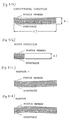
- Embodiments of the invention will now be described, by way of example only, with reference to the accompanying drawings in which:-
- FIG. 1 is an exploded perspective view of an element according to the present invention;
- FIG. 2 is a cross-sectional view of a gas sensor according to the present invention;
- FIG. 3 (a) is a schematic representation for explaining d1;
- FIG. 3 (b) is a schematic representation for explaining d2;
- FIGS 3 (c) and (d) are Schematic representations for explaining warpage of an element.
-
- Reference numerals are used to identify items shown in the drawings as follows:
- 1: gas sensor element
- 11a: first substrate
- 11b : second substrate
- 111a: through-hole
- 12: heating resistor
- 121: heating portion
- 122: heater lead portion
- 13: buffer layer
- 14a: reference electrode
- 14b: detection electrode
- 15a: first solid electrolytic member
- 15b: second solid electrolytic member
- 16a: first insulating layer
- 16b: second insulating layer
- 161a,161b: through-hole
- 17: porous member
- 18a: first reinforcing layer
- 18b: second reinforcing layer
- 2: gas sensor
- 21: metallic shell
- 211: metallic shell screw portion
-
- With reference to Figs. 1, 2 and 3, the present invention will next be described in more detail by way of embodiments.
- In order to simplify description, the production process will be described by taking, as an example, production of an element in which patterns are printed on a sheet having a size of one element, and layers are laminated. However, in practice, patterns were formed through printing on a green sheet having a large size such that a plurality of elements can be produced; layers were laminated; the resultant multi-layer product was cut into green products having an element shape; and each green product was subjected to degreasing and firing, to thereby produce an element.
- Alumina powder (purity: 99.99% or more, mean particle size: 0.3 µm) (100 parts by mass (hereinafter simply referred to as "parts")) was mixed with a butyral resin (14 parts) and dibutyl phthalate (7 parts). The resultant mixture was mixed with a solvent mixture of toluene and methyl ethyl ketone, to thereby prepare a slurry. A green sheet for a first substrate and a green sheet for a second substrate were formed from the slurry through a doctor blade process. Subsequently, through holes 111a were formed at predetermined positions of the green sheet for a first substrate. The green sheet for a first substrate has a thickness of 0.45 mm, a length of 5 cm, and a width of 4.5 mm. After being fired, the green sheet becomes a first substrate 11a. The green sheet for a second substrate has a thickness of 0.25 mm, a length of 5 cm, and a width of 4.5 mm. After being fired, the green sheet becomes a second substrate 11b.
- Alumina powder (purity: 99.99% or more, mean particle size: 0.3 µm) (4 parts) was mixed with platinum powder (100 parts). To the resultant mixture were added a binder (6 parts) and dibutyl phthalate (25 parts), to thereby prepare a paste for a conductive layer. Through printing, the paste was applied in a heating portion pattern (i.e., a
heating portion 121 after firing) onto a first surface of the green sheet for a first substrate (i.e., a first substrate 11a after firing) and dried. Subsequently, through printing, the paste was applied in a heater lead pattern (i.e., a heater lead portion 122 after firing) onto the first surface of the green sheet and dried, to thereby form a heater pattern (i.e., heating resistor 12 after firing). Subsequently, through printing, the paste was applied in heating resistor terminal patterns (i.e., heating resistor terminals 19a after firing) in the vicinity of the end of a second surface of the green sheet for a first substrate, such that the heating resistor 12 conducted to the terminals 19a through the through holes 111a, and the paste was dried. Thereafter, the green sheet for a second substrate (i.e., the upper half of the substrate after firing) was formed on the heater pattern, and connected to the green sheet for a first substrate through pressing. - Alumina (80 parts) was mixed with a zirconia (20 parts), to thereby prepare a paste for a buffer layer. Through printing, the paste was applied in a buffer layer pattern (i.e., a buffer layer 13 after firing) (thickness: 40 ± 10 µm) onto the green sheet for a second substrate of the ceramic multi-layer product formed in step (2), and the paste was dried.
- A paste for electrode formation was prepared in the same manner as that used for preparing the paste for a conductive layer used in the step (2), except that powder of partially-stabilized zirconia (20 parts) (purity: 99.9% or more, mean particle size: 0.3 µm) was used in place of alumina powder. Through printing, the paste for electrode formation was applied in a reference electrode pattern (i.e., a reference electrode 14a after firing) (thickness: 20 ± 10 µm) including a reference electrode portion pattern (i.e., a reference electrode portion 141a after firing) and a reference electrode lead portion pattern (i.e., a reference electrode lead portion 142a after firing) onto the buffer layer pattern formed in step (3), and the paste was dried.
- To zirconia powder (purity: 99.9% or more, mean particle size: 0.3 µm) (50 parts) were added alumina powder (purity: 99.99% or more, mean particle size: 0.3 mm) (50 parts), butylcarbitol (33.3 parts), dibutyl phthalate (0.8 parts), a dispersant (0.5 parts), a binder (20 parts), and acetone (a predetermined amount), and the resultant mixture was mixed for four hours. Subsequently, acetone was evaporated, to thereby prepare a paste for a solid electrolytic member.
- The paste for a solid electrolytic member was applied through printing so as to cover the reference electrode pattern and dried, to thereby form a first solid electrolytic member pattern (i.e., a first solid electrolytic member 15a after firing) having a length of 13 mm and a thickness of 25 ± 10 µm.
- Butylcarbitol (50 parts) and acetone (a predetermined amount) were added to the slurry for a green sheet prepared in step (1), and the resultant mixture was mixed for four hours. Subsequently, acetone was evaporated, to thereby prepare a paste for an insulating layer. Through printing, the paste for an insulating layer was applied onto a portion of the buffer layer pattern on which the first solid electrolytic pattern had not been printed, and dried, to thereby form a first insulating layer pattern (i.e., a first insulating layer 16a after firing) having a thickness of 25 ± 10 µm. The paste was not applied onto a portion corresponding to a through-hole 161a.
- Through printing, the paste for a solid electrolytic member prepared in the step (5) was applied onto the first solid electrolytic member so as to form a second solid electrolytic member pattern (i.e., a second solid electrolytic member 15b after firing), which extends from the tip end portion and has a length of 6.5 mm and a thickness of 25 ± 10 µm.
- Through printing, the paste for an insulating layer prepared in the step (6) was applied onto the first solid electrolytic pattern and the first insulting layer pattern so as to cover a portion on which the second solid electrolytic pattern had not been printed, and dried, to thereby form a second insulating layer pattern (i.e., a second insulating layer 16b after firing) having a thickness of 25 ± 10 µm. The paste was not applied onto a portion corresponding to the through-hole 161b.
- Through printing, the paste for a conductive layer prepared in the step (4) was applied onto the second solid electrolytic member pattern formed in step (7) and the second insulating layer pattern formed in step (8) in a detection electrode pattern (i.e., a detection electrode 14b after firing) (thickness: 20 ± 10 µm) including a detection electrode portion pattern (i.e., a detection electrode portion 141b after firing) and a detection electrode lead portion pattern (i.e., a detection
electrode lead portion 142b after firing), and the paste was dried. - The raw materials employed in step (1) were mixed in the same compositional proportions as those described in step (1), to thereby prepare a slurry. A green sheet for a first reinforcing layer and a green sheet for a second reinforcing layer were formed from the slurry through a doctor blade process. The green sheet for a first reinforcing layer has a thickness of 0.25 mm and a length of 3.5 cm. After being fired, the green sheet becomes a first reinforcing layer 18a. Through-holes 181 a are formed at the end portion of the green sheet. The green sheet for a second reinforcing layer has a thickness of 0.4 mm and a length of 3.5 cm. After being fired, the green sheet becomes a second reinforcing layer 18b. Through-holes 181b are formed at the end portion of the green sheet.
- Subsequently, the green sheet for a first reinforcing layer was laminated so as to cover the detection electrode lead portion pattern of the detection electrode pattern formed in step (9). Thereafter, the green sheet for a second reinforcing layer was laminated onto the green sheet for a first reinforcing layer.
- Through printing, the conductive paste prepared in step (4) was applied in electrode terminal patterns (i.e., electrode terminals 19b after firing) onto positions corresponding to the through-holes 181b, and dried. The electrode terminals are employed for inputting or outputting electric signals to or from each of the reference electrode and the detection electrode.
- In a manner similar to that of step (1), alumina powder (purity: 99.99% or more, mean particle size: 0.3 µm) (100 parts) was mixed with carbon powder (spherical powder, mean particle size: 7.5 µm) (30 parts), a butyral resin (12 parts), and dibutyl phthalate (6 parts). The resultant mixture was mixed with a solvent mixture of toluene and methyl ethyl ketone, to thereby prepare a slurry. Through a doctor blade process, the slurry was shaped into a sheet having a thickness of 450 µm. Subsequently, the resultant sheet was cut into pieces having a length of 10 mm and a width of 4.5 mm, to thereby prepare green sheets for a porous member.
- The resultant green sheet for a porous member (i.e., a
porous member 17 after firing) was laminated so as to cover the detection electrode portion pattern formed in step (9). - In order to prepare the green sheet for a porous member, a paste for the green sheet was prepared such that, when the mass of a binder for the substrate on the basis of unit surface area of ceramic raw material powder (alumina) for the substrate is referred to as "B1" (g/m2), and the mass of a binder for the porous member (butyral resin) on the basis of unit surface area of ceramic raw material powder for the porous member is referred to as "B2" (g/m2), the value X represented by the following formula [3] falls within a range between -0.1 and 0.1.
- When the paste is prepared as described above, the amount of the binder on the basis of unit surface area of ceramic raw material powder for the green sheets for first and second substrates is substantially equal to that of the binder on the basis of unit surface area of ceramic raw material powder for the green sheet for the porous member. Therefore, the difference in shrinkage percentage between the green sheet for the substrate and the green sheet for the porous member can be maintained within 7% during firing at a temperature of 1,200-1,500°C.
- The temperature of the multi-layer product formed in steps (1) through (12) was elevated in air from room temperature to 420°C at a rate of 10°C/hour. Subsequently, the temperature of the product was maintained at 420°C for two hours, to thereby remove the organic binder from the product. Thereafter, the temperature of the product was elevated in air to 1,100°C at a rate of 100°C/hour, and then elevated to 1,520°C at a rate of 60°C/hour. The temperature of the product was maintained at 1,520°C for one hour for firing the product, to thereby produce an
element 1. - The percentage of alumina powder or zirconia powder which was incorporated into the green sheet in steps (1) and (12) of the steps (1) through (12) in [1] and the particle size of the powder were changed, to thereby produce elements in which the volume percent of a ceramic component of highest volume percent contained in the substrate or the porous member and the mean grain size of crystals differed (300 elements for each of Test Examples 1 through 24). In each Test Example, five elements were randomly selected from the 300 elements, R1, R2, and R2/R1 in relation to each of the five elements were calculated, and the average values of R1, R2, and R2/R1 were obtained. The results are shown in Tables 1 and 2. Furthermore, in each Test Example, one element was randomly selected from the 300 elements, and a micrograph of the element was obtained by use of an electron microscope. By use of the micrograph, a1, a2, and a1/a2 in relation to the element were calculated. The results are shown in Tables 1 and 2.


- Five elements were randomly selected from the elements produced through the procedures [1] and [2], and the degree of warpage of the five elements was measured by calculating the average of "d1 - d2" {see FIGs. 3(a) and 3(b)} of the elements immediately after firing. The results are shown in Tables 1 and 2. Furthermore, each of the five elements was placed such that the porous member was on the upper side. When the element was curled upward, "+" was assigned to the value "d1 - d2," and when the element was curled downward, "-" was assigned to the value "d1 - d2" {see FIGs. 3(c) and 3(d)}. The results are shown in Tables 1 and 2.
- In addition, all the 300 elements of each of Test Examples 1 through 24 were subjected to vacuum immersion in water-soluble red ink for 10 minutes, and then washed with water. Thereafter, exfoliation and cracking of each element were observed. The results are shown in Tables 1 and 2.
- All the elements of each of Test Examples 1 through 24 produced through the procedure [1] and [2], except the elements which suffered exfoliation and cracking after firing, were subjected to the following heating cycle test: a voltage of 16 V was applied to the heating resistor of each element, to thereby heat the element until the temperature of the solid electrolytic member reached about 1,000°C; and subsequently, application of the voltage was stopped, and the element was allowed to stand until the temperature of the solid electrolytic member was lowered to room temperature. The heating cycle test was repeated 10 times for each element. Thereafter, exfoliation and cracking of each element were observed in a manner similar to that of [3]. The results are shown in Tables 1 and 2.
- In each of Test Examples 25 through 31, the procedure of [1] was repeated, except that the amount of carbon powder was changed in step (12), to thereby produce an element including a porous member having a relative density and a porosity shown in Table 3.
- Subsequently, an oxygen sensor including the resultant element was provided in the discharge system of a heated engine of 1,800 cc, and the response speed of the sensor was evaluated when the ratio of fuel to air was changed every three seconds so as to attain rich and lean states. The engine was operated by use of gasoline containing lead (Pb) in an amount of 50 mg per gallon of gasoline, and gasoline. The response speed of the oxygen sensor was evaluated after 500 hours of the engine exhaust gas exposure cycles of 450 °C (1 hour) - 850°C (3 hours). The results are shown in Table 3.
- Furthermore, the engine was operated by use of gasoline containing 0.12 cc silicon (Si) per liter of gasoline. The response speed of the oxygen sensor was evaluated after 18 hours of the engine exhaust gas exposure of 400°C. The test result are shown table 3.
- Still furthermore, the engine was operated by use of gasoline containing 0.3g of phosphorus (P) per liter of gasoline. The response speed of the oxygen sensor was evaluated after 18 hours of the engine exhaust gas exposure of 400°C. The test result are shown in Table 3.
- In order to evaluate the response speed, a voltage of 14 V was applied to the heating resistor, to thereby regulate the temperature of the solid electrolytic member at 700°C.

- As is apparent from Tables 1 and 2, immediately after firing and after the cooling-heating cycle test, no major exfoliation and cracking are observed in gas sensor elements according to the first invention; i.e., all 300 gas sensor elements of each Test Example, except the elements of Test Examples 8, 9, 17, 18, 22, 23, and 24, although minor cracking is observed in some of the 300 elements of Test Examples 1, 5 and 6 after the cooling-heating cycle test. Therefore, the element according to the first invention exhibits excellent durability.
- As is apparent from Table 3, when a porous member has a relative density of 41-79% and a porosity of 21-59%, the element including the porous member exhibits excellent durability. The results shown in Table 3 show that the elements of Test Examples 25 and 26 exhibit unsatisfactory durability with respect to SiO2 microparticles in gasoline. The results also show that the element of Test Example 31 exhibits unsatisfactory durability with respect to a poisoning substance having a relatively large particle size. The results also show that the element of Test Example 31 exhibits unsatisfactory responsiveness even at an initial stage, since the porosity of the porous member is very low.
- Thus, the elements having the structure as described in the first and second inventions and the structure as described in the third and fourth inventions exhibit satisfactory responsiveness and excellent durability.
- The element of the present invention usually has a length of 37.5 mm. When the element shown in FIG. 1 is employed, a portion of the element which is about 29.2 mm distant from the back end side of the porous member (the term "back end" refers to the end of the element in a longitudinal direction at which the porous member is not formed) is fixed with a fixing member provided in a metallic shell of a gas sensor. Therefore, the portion is not exposed to a gas to be detected, and the element barely warps during use.
- According to one aspect of the present invention, there can be produced a multi-layer gas sensor element including a porous body, which element does not produce warpage and barely suffers exfoliation and cracking during use; i.e., which element exhibits high durability. According another aspect of the present invention, a gas sensor exhibiting high durability can be produced.
Claims (10)
- A multi-layer gas sensor element comprising a solid electrolytic member (15a, 15b), a substrate (11a, 11b), and a porous member (17), characterized in that each of the substrate (11a, 11b) and the porous member (17) has a thickness larger than that of the solid electrolytic member (15a, 15b) with respect to a lamination direction; the substrate (11a, 11b) and the porous member (17) face each other and sandwich the solid electrolytic member (15a, 15b); and a ceramic component constituting the substrate (11a, 11b), and having the highest volume percent of the substrate (11a, 11b), is the same as the ceramic component constituting the porous member (17) and having the highest volume percent of said porous member (17); and the volume percent (R2) of said ceramic component contained in the porous member (17) is 80% or more of the volume percent (R1) of said ceramic component contained in the substrate (11a, 11b).
- A multi-layer gas sensor element according to claim 1, wherein, when the mean grain size of crystals constituting the substrate (11a, 11b) is referred to as "a1" and the mean grain size of crystals constituting the porous member (17) is referred to as "a2," a value A represented by the following equation:
- A multi-layer gas sensor element according to claim 1 or 2, wherein the relative density of the porous member (17) is 40-85%.
- A multi-layer gas sensor element according to any one of claims 1 to 3, wherein the porosity of the porous member (17) is 15-60%.
- A multi-layer gas sensor element according to any one of the preceding claims, wherein the thickness of each of the substrate (11a, 11b) and the porous member (17) is at least 1.5 times the thickness of the solid electrolyte member.
- A multi-layer gas sensor element according to any one of the preceding claims, wherein the amount of said ceramic component of highest volume percent contained in the substrate (11a, 11b) is 80 vol% or more.
- A multi-layer gas sensor element according to any one of the preceding claims, wherein the volume percent (R2') of crystals formed of said ceramic component of highest volume percent contained in the porous member (17) is 60% or more of the volume percent (R1') of crystals formed of said ceramic component contained in the substrate (11a, 11b).
- A multi-layer gas sensor element according to any one of the preceding claims, wherein said ceramic component of highest volume percent is Al2O3 or ZrO2.
- A multi-layer gas sensor element according to any one of the preceding claims, wherein the solid electrolytic member (15a, 15b) also contains said ceramic component which is predominantly contained in said substrate (11a, 11b), preferably in an amount of 20 to 70 mass%.
- A gas sensor comprising a multi-layer gas sensor element according to any one of the preceding claims.
Applications Claiming Priority (2)
| Application Number | Priority Date | Filing Date | Title |
|---|---|---|---|
| JP2000232400 | 2000-07-31 | ||
| JP2000232400 | 2000-07-31 |
Publications (2)
| Publication Number | Publication Date |
|---|---|
| EP1191333A1 true EP1191333A1 (en) | 2002-03-27 |
| EP1191333B1 EP1191333B1 (en) | 2007-10-03 |
Family
ID=18725093
Family Applications (1)
| Application Number | Title | Priority Date | Filing Date |
|---|---|---|---|
| EP01306547A Expired - Lifetime EP1191333B1 (en) | 2000-07-31 | 2001-07-31 | Multi-layer gas sensor element and gas sensor comprising the same |
Country Status (3)
| Country | Link |
|---|---|
| US (1) | US6746586B2 (en) |
| EP (1) | EP1191333B1 (en) |
| DE (1) | DE60130720T2 (en) |
Families Citing this family (15)
| Publication number | Priority date | Publication date | Assignee | Title |
|---|---|---|---|---|
| US6634210B1 (en) * | 2002-04-17 | 2003-10-21 | Delphi Technologies, Inc. | Particulate sensor system |
| US20090101502A1 (en) * | 2003-02-10 | 2009-04-23 | Robert Bosch Gmbh | Thermal Shock Resistant Gas Sensor Element |
| US8906214B2 (en) * | 2003-02-10 | 2014-12-09 | Robert Bosch Gmbh | Contamination-resistant gas sensor element |
| US7211180B2 (en) * | 2003-02-10 | 2007-05-01 | Robert Bosch Corporation | Contamination-resistant gas sensor element |
| JP4228975B2 (en) * | 2004-04-15 | 2009-02-25 | 株式会社デンソー | Multilayer gas sensor element |
| DE102004034192A1 (en) * | 2004-07-14 | 2006-02-09 | Heraeus Sensor Technology Gmbh | Platform chip useful in gas sensors comprises a conductor structure comprising an electrically conductive oxide and/or comprising components with durable stable resistance characteristics at high temperatures |
| JP2006222068A (en) * | 2005-01-14 | 2006-08-24 | Denso Corp | Ceramic heater and its manufacturing method |
| AT8257U1 (en) * | 2005-04-19 | 2006-04-15 | Electrovac | SENSOR ARRANGEMENT |
| US20080006532A1 (en) * | 2005-04-19 | 2008-01-10 | Rangachary Mukundan | Ammonia and nitrogen oxide sensors |
| JP4680662B2 (en) * | 2005-04-26 | 2011-05-11 | 日本特殊陶業株式会社 | Gas sensor |
| JP5198832B2 (en) * | 2007-11-06 | 2013-05-15 | 日本特殊陶業株式会社 | Gas sensor |
| JP4575470B2 (en) * | 2008-03-27 | 2010-11-04 | 日本碍子株式会社 | Sensor element and gas sensor |
| JP6754559B2 (en) | 2015-09-29 | 2020-09-16 | 日本碍子株式会社 | Gas sensor |
| KR101724499B1 (en) * | 2015-12-11 | 2017-04-07 | 현대자동차 주식회사 | Particulate matter sensor and measurement method thereof |
| CN109738492A (en) * | 2018-12-20 | 2019-05-10 | 广州奥松电子有限公司 | A kind of production method of gas sensor sensitive material |
Citations (5)
| Publication number | Priority date | Publication date | Assignee | Title |
|---|---|---|---|---|
| EP0059933A1 (en) * | 1981-03-06 | 1982-09-15 | Nissan Motor Co., Ltd. | Solid electrolyte oxygen sensing element of laminated structure with gas diffusion layer on outer electrode |
| US4595485A (en) * | 1983-03-14 | 1986-06-17 | Kabushiki Kaisha Toyota Chuo Kenkyusho | Limiting electric current type oxygen sensor |
| US4661234A (en) * | 1984-12-28 | 1987-04-28 | Kabushiki Kaisha Toyota Chuo Kenkyusho | Air-fuel ratio sensor and apparatus using the same |
| US4798693A (en) * | 1984-04-26 | 1989-01-17 | Ngk Insulators, Ltd. | Method of manufacturing an electrochemical device |
| EP0686847A2 (en) * | 1994-06-09 | 1995-12-13 | Nippondenso Co., Ltd. | Oxygen concentration detector |
Family Cites Families (3)
| Publication number | Priority date | Publication date | Assignee | Title |
|---|---|---|---|---|
| DE2810134A1 (en) * | 1978-03-09 | 1979-09-20 | Bosch Gmbh Robert | ZIRCONIUM OXIDE CERAMICS WITH A FINE-GRAY AND THERMALLY STABLE STRUCTURE AND HIGH THERMAL SHOCK RESISTANCE, MOLDED BODIES MANUFACTURED FROM THEM, METHOD FOR MANUFACTURING THE MOLDED BODIES AND THEIR USE |
| JPH0617891B2 (en) * | 1984-07-06 | 1994-03-09 | 日本電装株式会社 | Oxygen concentration detector |
| JP3475548B2 (en) | 1994-04-19 | 2003-12-08 | 株式会社デンソー | Layered ceramic body, oxygen sensor and method for producing the same |
-
2001
- 2001-07-31 DE DE60130720T patent/DE60130720T2/en not_active Expired - Lifetime
- 2001-07-31 US US09/917,874 patent/US6746586B2/en not_active Expired - Fee Related
- 2001-07-31 EP EP01306547A patent/EP1191333B1/en not_active Expired - Lifetime
Patent Citations (5)
| Publication number | Priority date | Publication date | Assignee | Title |
|---|---|---|---|---|
| EP0059933A1 (en) * | 1981-03-06 | 1982-09-15 | Nissan Motor Co., Ltd. | Solid electrolyte oxygen sensing element of laminated structure with gas diffusion layer on outer electrode |
| US4595485A (en) * | 1983-03-14 | 1986-06-17 | Kabushiki Kaisha Toyota Chuo Kenkyusho | Limiting electric current type oxygen sensor |
| US4798693A (en) * | 1984-04-26 | 1989-01-17 | Ngk Insulators, Ltd. | Method of manufacturing an electrochemical device |
| US4661234A (en) * | 1984-12-28 | 1987-04-28 | Kabushiki Kaisha Toyota Chuo Kenkyusho | Air-fuel ratio sensor and apparatus using the same |
| EP0686847A2 (en) * | 1994-06-09 | 1995-12-13 | Nippondenso Co., Ltd. | Oxygen concentration detector |
Also Published As
| Publication number | Publication date |
|---|---|
| US6746586B2 (en) | 2004-06-08 |
| DE60130720T2 (en) | 2008-07-17 |
| US20020036138A1 (en) | 2002-03-28 |
| DE60130720D1 (en) | 2007-11-15 |
| EP1191333B1 (en) | 2007-10-03 |
Similar Documents
| Publication | Publication Date | Title |
|---|---|---|
| EP1191333A1 (en) | Multi-layer gas sensor element and gas sensor comprising the same | |
| US7041207B2 (en) | Solid electrolyte containing insulating grains for gas sensor | |
| EP1197748A1 (en) | Humidity sensor | |
| EP0294085B1 (en) | Electrochemical elements | |
| US5278007A (en) | Electrochemical element and method of producing same | |
| US8545684B2 (en) | Sensing element and method of making the same | |
| EP1346210A2 (en) | Gas sensor | |
| JP3467814B2 (en) | Oxygen concentration detector | |
| KR20010021013A (en) | Solid electrolyte containing insulating ceramic grains for gas sensor, and method for fabricating same | |
| CN110274942B (en) | Sensor element and gas sensor | |
| JP3683348B2 (en) | Manufacturing method of ceramic structure | |
| JP4125849B2 (en) | Oxygen sensor element | |
| JP4583187B2 (en) | Ceramic heater element and detection element using the same | |
| JP2002286680A (en) | Lamination type gas sensor element and its manufacturing method | |
| JP4473471B2 (en) | Laminated gas sensor element and gas sensor including the same | |
| JP4588853B2 (en) | Manufacturing method of laminated gas sensor element | |
| JP2001064082A (en) | Ceramic sintered body, its production, gas sensor element and its production | |
| US4857165A (en) | Oxygen sensing element and process of manufacturing the same | |
| JP2002365258A (en) | Gas sensor element, its manufacturing method and gas sensor | |
| JP3310358B2 (en) | Solid electrolyte device and method for manufacturing the same | |
| JP3793563B2 (en) | Manufacturing method of oxygen sensor | |
| US20020117397A1 (en) | Exhaust oxygen sensor electrode formed with organo-metallic ink additives | |
| JP4579636B2 (en) | Manufacturing method of gas sensor | |
| JP4166404B2 (en) | Gas sensor element and gas sensor including the same | |
| JP2001348265A (en) | Alumina-based sintered compact, method of producting the same, ceramic heater and gas sensor element using the sintered compact, and gas sensor using the gas sensor element |
Legal Events
| Date | Code | Title | Description |
|---|---|---|---|
| PUAI | Public reference made under article 153(3) epc to a published international application that has entered the european phase |
Free format text: ORIGINAL CODE: 0009012 |
|
| AK | Designated contracting states |
Kind code of ref document: A1 Designated state(s): DE FR IT Kind code of ref document: A1 Designated state(s): AT BE CH CY DE DK ES FI FR GB GR IE IT LI LU MC NL PT SE TR |
|
| AX | Request for extension of the european patent |
Free format text: AL;LT;LV;MK;RO;SI |
|
| 17P | Request for examination filed |
Effective date: 20020916 |
|
| AKX | Designation fees paid |
Free format text: DE FR IT |
|
| 17Q | First examination report despatched |
Effective date: 20040709 |
|
| GRAP | Despatch of communication of intention to grant a patent |
Free format text: ORIGINAL CODE: EPIDOSNIGR1 |
|
| GRAS | Grant fee paid |
Free format text: ORIGINAL CODE: EPIDOSNIGR3 |
|
| GRAA | (expected) grant |
Free format text: ORIGINAL CODE: 0009210 |
|
| AK | Designated contracting states |
Kind code of ref document: B1 Designated state(s): DE FR IT |
|
| REF | Corresponds to: |
Ref document number: 60130720 Country of ref document: DE Date of ref document: 20071115 Kind code of ref document: P |
|
| ET | Fr: translation filed | ||
| PLBE | No opposition filed within time limit |
Free format text: ORIGINAL CODE: 0009261 |
|
| STAA | Information on the status of an ep patent application or granted ep patent |
Free format text: STATUS: NO OPPOSITION FILED WITHIN TIME LIMIT |
|
| 26N | No opposition filed |
Effective date: 20080704 |
|
| PG25 | Lapsed in a contracting state [announced via postgrant information from national office to epo] |
Ref country code: IT Free format text: LAPSE BECAUSE OF NON-PAYMENT OF DUE FEES Effective date: 20080731 |
|
| PGFP | Annual fee paid to national office [announced via postgrant information from national office to epo] |
Ref country code: FR Payment date: 20140708 Year of fee payment: 14 |
|
| REG | Reference to a national code |
Ref country code: FR Ref legal event code: ST Effective date: 20160331 |
|
| PG25 | Lapsed in a contracting state [announced via postgrant information from national office to epo] |
Ref country code: FR Free format text: LAPSE BECAUSE OF NON-PAYMENT OF DUE FEES Effective date: 20150731 |
|
| PGFP | Annual fee paid to national office [announced via postgrant information from national office to epo] |
Ref country code: DE Payment date: 20170725 Year of fee payment: 17 |
|
| REG | Reference to a national code |
Ref country code: DE Ref legal event code: R119 Ref document number: 60130720 Country of ref document: DE |
|
| PG25 | Lapsed in a contracting state [announced via postgrant information from national office to epo] |
Ref country code: DE Free format text: LAPSE BECAUSE OF NON-PAYMENT OF DUE FEES Effective date: 20190201 |