Field of Technology
This invention concerns light source equipment that includes what is called a dielectric-barrier
discharge lamp, which is a type of discharge lamp used, for example, as a source of
ultraviolet radiation for photochemical reactions, in which eximer molecules are formed by
dielectric-barrier discharge, and which uses light emitted from the excimer molecules.
Background of Technology
Technical literature explaining the technology involved in the dielectric-barrier discharge
lamps with which this invention is concerned can be found in, for example, JPO kokai patent
report H2-7353. This document describes an emitter that produces light by causing the
formation of eximer molecules by means of a dielectric barrier discharge in a discharge
chamber filled with a discharge gas that forms eximer molecules, and using the light radiated
by those eximer molecules (a dielectric barrier discharge is also known as ozonizer discharge
or silent discharge; see Denki Gakkai, "Discharge Handbook," revised edition, 7th printing,
June 1989, p. 263).
Dielectric-barrier discharge lamps have a discharge plasma space and one or two dielectrics
sandwiched between electrodes. Figure 19(a) shows a dielectric-barrier discharge lamp 1
with two dielectrics 5, 6. In figure 19(a), by the way, the lamp seal 7 also serves as two
dielectrics 5,6.
When lighting up the dielectric-barrier discharge lamp 1, a high-frequency, alternating current
of, for example 10 to 200 kHz and 2 to 10 kV is imposed on the electrodes 3,4.
However, because of the dielectrics 5,6 between the discharge plasma space 2 and the
electrodes 3,4, current does not flow directly from the electrodes 3,4 to the discharge plasma
space 2; the current flows by means of the action of the dielectrics 5,6 as a condenser. In
other words, a charge equal in size and opposite in sign to that on electrodes 3,4 is induced on
the discharge plasma space side of the dielectrics 5,6 because of polarization of the dielectric.
The discharge occurs between the dielectrics 5,6 that face across the discharge plasma space
2.
Little current flows along the discharge plasma space 2 side of the dielectrics 5,6; when
discharge occurs, the charge induced on the discharge plasma space 2 side of the dielectrics
5,6 is neutralized by the charge moved by the discharge, and the electrical field within the
discharge plasma space 2 is reduced. For that reason, the current stops even if the voltage
continues to be impressed on the electrodes 3,4. But when the voltage impressed on the
electrodes 3,4 rises again, the discharge current continues.
When the discharge ceases after having occurred, there is no further discharge until the
polarity of the voltage impressed on the electrodes 3,4 has reversed.
In the case of a dielectric-barrier discharge lamp in which xenon gas, for example, is sealed,
the xenon gas is dissociated into ions and electrons by the discharge, and becomes xenon
plasma. When the xenon plasma is excited to a specified energy level, eximer molecules are
formed within the plasma. Xenon eximers divide after a certain lifespan, but the energy
released at that time is emitted as a photon of vacuum ultraviolet wavelength. To make a
dielectric-barrier discharge lamp work efficiently as a vacuum ultraviolet light source, it is
necessary to form the eximer molecules efficiently.
The greatest obstacle to efficient formation of eximer molecules during discharge is the
excitation of the discharge plasma to energy levels that do not contribute to the formation of
eximer molecules.
The movement of discharge plasma electrons immediately after discharge begins is
collective, and the energy is high but the temperature is low. In this state, the discharge
plasma has a high probability of transition to the resonant state required for formation of
eximer molecules. If the discharge time is prolonged, however, the movement of the plasma
electrons gradually becomes thermal. That is, it reaches a state of thermal equilibrium known
as a Maxwell-Boltzmann distribution; the plasma temperature rises, and there is an increased
probability of transition to a state of higher excitation where eximer molecules cannot form.
Moreover, sometimes when eximer molecules have been formed, a subsequent discharge will
break down the eximer molecules before their -lifespan elapses and they divide naturally by
emitting the desired photon. In fact, in the case of xenon eximers, a period of about 1 µs is
required between the beginning of discharge and emission of a vacuum ultraviolet photon,
and a subsequent discharge or redischarge during that period reduces the efficiency of eximer
light emission.
In other words, once discharge had commenced, it is most important to reduce as much as
possible the energy of subsequent discharges.
Even in the event that the discharge time is short, if the energy injected during the discharge
period is too great, there is similarly an increased probability of transition to a state of high
excitation. Plasma that has transitioned to a state of high excitation moderates itself by
emission of infrared radiation, which just raises the temperature of the lamp and does not
contribute to eximer light emission.
That is, the discharge must be driven so as to suppress the excitation of discharge plasma to
energy levels that do not contribute to the formation of eximer molecules. That point is one
that cannot be satisfied by conventional dielectric-barrier discharge lamp light source
equipment.
JPO kokai patent report H1-243363 is a proposal to achieve eximer light emission with high
efficiency by means of all pulse discharges, including dielectric-barrier discharges. This
follows the condition stated above that once a discharge has begun, the energy of the
subsequent discharge is reduced as much as possible. However, what is described in this
proposal is which parameters to control to increase the efficiency of eximer light emission;
there is no specific mention of the effective conditions for those parameter values.
Particularly in the case of dielectric-barrier discharges, there is little freedom for control of
the voltage that has to be impressed and the current that has to be injected into the discharge
plasma space through the dielectric, and it is extremely difficult to discover the optimum
conditions.
There are proposals to improve the efficiency of dielectric-barrier discharge lamps, such as
JPO patent report H8-508363 (US patent 5,604, 410). However, these reports say nothing
about specific items that are truly effective in achieving control of the excitation of discharge
plasma to energy levels that do not contribute to formation of eximer molecules, so as to form
eximer molecules efficiently. There are descriptions of the results of experiments on
variation of brightness relative to variation of impressed voltage, in connection with
frequency and duty cycle, with regard to short pulse arrays and short waveforms, as well as
explanations of improvement of efficiency relative to conventional sinewave drive.
Actual power supplies, however, include high-voltage transformers, and are unable to impress
ideal short pulse arrays and short waveforms; because of interaction of the output impedance
of the power supply and the impedance of the lamp, the waveform lacks precision, and partial
resonance causes a sinewave voltage to be impressed.
In the event of discrepancies from ideal short waveforms in such actual power supplies,
unless it is clear what degree of discrepancy is allowed, it is not possible to design or
manufacture practical light source equipment economically.
This invention was made in consideration of the situation described above; its purpose is to
provide dielectric-barrier discharge lamp light source equipment that can produce eximer
molecules efficiently and operate efficiently as a vacuum ultraviolet light source.
Presentation of Invention
In order to form eximer molecules efficiently, which is the task of the invention of this
application, the excitation of discharge plasma at energy levels that will not contribute to the
formation of eximer molecules is controlled. To accomplish that, once the voltage impressed
on the lamp has climbed at a limited rate of ascent, reached the voltage for the
commencement of discharge and started the discharge, then the discharge should be stopped
as quickly as possible.
Operation of the electrical circuitry of the dielectric-barrier discharge lamp 1 is explained by
figure 19(b). As shown in figure 19(b), the discharge path of the discharge plasma space 2
continues in series with a resistor 10 and a switch 11. The dielectric-barrier discharge lamp 1
has dielectrics 5,6 between the electrodes 3,4 and the discharge plasma space 2, and it
functions as a condenser within the electrical circuitry. In the event that there are two pieces
of dielectric, however, the two condensers can be thought of as a single condenser 13.
Because the structure has this condenser inserted in series with the discharge plasma space 2,
discharge current flows through the dielectric-barrier discharge lamp 1 only for a period
immediately after the change in polarity of the voltage impressed on the lamp, and a non-discharge
period occurs naturally, even without impressing voltage on the lamp as a pulse
voltage that has a rest period that is essentially zero voltage.
Moreover, discharge does not occur until the voltage of the discharge plasma space 2 reaches
the voltage for the commencement of discharge.
The discharge plasma space 2 itself forms a condenser 12, and when discharge begins, almost
all the energy stored in this condenser is expended, and so once the discharge begins, there is
no need for additional current to the dielectric-barrier discharge lamp 1 from the power
supply.
The unit area of the lamp wall surface is considered next.
The voltage for the commencement of discharge is decided almost automatically when the
gas pressure and the discharge gap are decided. And because the size of the discharge gap
determines the static capacity C1 of the condenser 12 formed by the discharge plasma space,
the minimum energy that can be put into the plasma between the commencement and
completion of a single discharge is the energy of a full discharge of the charge stored in the
condenser 12 formed by the discharge plasma space. That determines the constitution of the
lamp.
It was stated above that in order to form eximer molecules efficiently, the excitation of
discharge plasma at energy levels that will not contribute to the formation of eximer
molecules is controlled. That control is best achieved through the conditions for discharge of
that minimum energy.
However, the conditions for discharge of that minimum energy can be realized in an ideal
fashion by very slowly raising the voltage impressed on the lamp, and then discharging it,
using a power supply with an output impedance that is quite large.
There are, however, problems in applying such a power supply in an actual light source.
The first problem is that when the output impedance is large, it is not possible to operate fast
enough to discharge in cyclical repetitions.
The second problem is that under conditions for discharge of the minimum energy, there will
be a lack of uniformity of discharge within a single lamp because of a lack of positional
uniformity of the discharge gap within the lamp.
Accordingly, using a power supply that has the small output impedance that can realize the
necessary volume of light, in order to have a practical light source that produces uniform
discharges over the full surface of the dielectric-barrier discharge lamp, it is necessary to raise
the voltage impressed on the lamp beyond the minimum energy conditions for discharge.
However, the degree to which the voltage impressed on the lamp is raised should be held
below the range that would allow a drop in the efficiency of eximer light emission.
That is, the peak value of the voltage impressed on the lamp should be based on the lowest
value at which the lack of discharge uniformity can be ignored practically, and should be held
to 2 times that lowest value, preferably 1.5 times the lowest value. Or to base it on the lowest
value for maintaining the discharge, it should be held to 3 times, preferably 2.5 times that
lowest value. Now, when the lamp power is increased, it is done not by raising the voltage
impressed on the lamp, but by increasing the drive frequency of the lamp power supply.
Because a fixed volume of lamp current flows each time the voltage impressed on the lamp is
reversed, the lamp power is proportional to the drive frequency. Therefore, by increasing that
drive frequency, it is possible to increase the lamp power without the bad effects that would
accompany an increase of the voltage impressed on the lamp.
The basic constitution of the dielectric-barrier discharge lamp light source equipment is
shown in figure 1. In the figure, 1 is the dielectric-barrier discharge lamp described above,
and 8 is the power supply. The power supply 8 comprises a high-frequency alternating
current power supply 9 of the bridge, push-pull or fly-back type, and a step-up transformer
Tr.
Typical waveforms for the voltage impressed on the lamp E(t), the discharge gap voltage
(that is, the voltage of the discharge plasma space) Vl(t), lamp current Is(t) and discharge
current Id(t) of a practical power supply are shown in figure 2 (the figure shows waveforms
obtained from a computer simulation modelling the circuit and lamp based on a full-bridge
power supply, but they would be basically the same with a half-bridge or push-pull type
power supply).
Now with regard to the discharge current Id(t), it is the current in the lamp flowing through
the resistor in figure 19(b), so the waveform cannot be measured directly, but if it is possible
to measure the waveform data for the voltage impressed on the lamp E(t) and the lamp
current Is(t), it can be calculated from the static capacitance C1 of the condenser 12, which is
the discharge plasma space shown in figure 19(b), the static capacitance C2 of the condenser
13 which is the dielectrics 5,6, and floating static capacitance C3 which exists in parallel with
the dielectric-barrier discharge lamp.
That is, the static capacitance C1 of the condenser 12, which is the discharge plasma space,
the static capacitance C2 of the condenser 13 which is the dielectrics 5,6, and floating static
capacitance C3 which exists in parallel with the dielectric-barrier discharge lamp determine
the two relationships F = 1 + C1/C2 and Cv = C1 + C3 · F. Using that, the discharge current
Id(t) can be found from the following formula (1).
Id(t) = F · Is(t) - Cv · dE(t) / dt
Because this method uses numerical differentiation, the precision is not to good in regions
where the current values of the waveform obtained as a result are small, but it does indicate
the rapid rise when discharge commences, so there is no problem as long as it is used for that
purpose.
In figure 2, when the voltage impressed on the lamp E(t) suddenly changes polarity, the
discharge gap voltage Vl(t) also makes a quick change, and when it reaches the voltage for
the commencement of discharge at point G1, discharge commences. When discharge
commences, the discharge current waveform J1 (see the discharge current Id(t) waveform in
figure 2), rapidly appears, and as a result the discharge gap voltage Vl(t) drops suddenly. In
response to this sudden drop of the discharge gap voltage Vl(t) (that is, the voltage in the
discharge plasma space), the voltage impressed on the lamp E(t) also drops, producing the
indentation at point K.
The point on the voltage impressed on the lamp waveform that corresponds to point J2 where
the discharge current ceases is the point P1 with the largest absolute value, or slightly beyond
that. In evaluating actual light source equipment, that point can be taken as located at the
point P1 with the largest absolute value.
Thereafter, the change of the waveform of the voltage impressed on the lamp is reduced by
C2/(C1+C2) times, and the waveform of the discharge gap voltage Vl(t) is expressed as is.
As used here, C1 and C2 are the static capacitance C1 of the condenser 12, which is the
discharge plasma space, and the static capacitance C2 of the condenser 13 which is the
dielectrics 5,6, as described above. In the case of a dielectric-barrier discharge lamp that has
dielectrics 5,6 for both electrodes 3,4, C2 can be thought of as the independent static
capacitance of each dielectric, in series.
In a practical power supply, the voltage impressed on the lamp has an indentation at point K
for the following reason. In response to the sudden drop of the discharge gap voltage Vl(t)
(which is the voltage of the discharge plasma space) described above, the voltage impressed
on the lamp E(t) drops as well. The power supply 8 attempts to compensate for the drop in
the voltage impressed on the lamp, but because of the presence of an inductive output
impedance caused by the magnetic leakage of the step-up transformer or the inductance of the
cable, compensation for the drop in the voltage impressed on the lamp is delayed, and as a
result, the indentation in the direction of the greatest absolute value at point K is produced.
Moreover, because of resonance between this inductive output impedance and the static
capacitance of the dielectric-barrier discharge lamp 1, an oscillating component is
incorporated in the voltage impressed on the lamp following the indentation at point K. The
points with greatest absolute value and least absolute value are produced on the waveform of
the voltage impressed on the lamp as a result.
Hereafter, the oscillation that follows the indentation at point K is called ringing, and its
frequency is the ringing frequency Fr. The time period from the commencement of discharge
at point K to the peak value of the voltage impressed on the lamp E(t) is called τ, and the
period from the peak P1 that appears after the indentation at point K to the next peak P2 is
T12.
This invention focuses on variation of the waveform of the voltage impressed on the lamp
following the indentation at point K, and attempts to inject power into the dielectric-barrier
discharge lamp effectively, without lowering the efficiency of ultraviolet light emission.
That is, eximer molecules are produced by the discharge that occurs with the sudden rise or
fall of the waveform of the voltage impressed on the lamp E(t) as described above, and the
eximer molecules are broken down if further discharge current is added in the period before
the eximer molecules dissociate and produce ultraviolet radiation. Accordingly, it is desirable
from the perspective of efficient production of ultraviolet radiation to cut off the discharge
current quickly.
Nevertheless, the discharge current continues from the commencement of discharge at the
indentation at point K to the first peak of the voltage impressed on the lamp E(t). Therefore,
if there is a long period τ from the commencement of discharge until the voltage impressed
on the lamp peaks, the efficiency of ultraviolet radiation is reduced as a result.
Moreover, in the state where ringing occurs following the indentation at point K, the
discharge current continues until the peak is reached. Thus when the ringing frequency is
low, it takes longer for the discharge current to cease, and the efficiency of ultraviolet
radiation is reduced as a result.
In other words, a dielectric-barrier discharge lamp can be made to discharge without reducing
the efficiency of ultraviolet light emission by shortening the period τ from the
commencement of discharge to the first peak of the voltage impressed on the lamp, or by
increasing the ringing frequency Fr.
In this case, the period τ from the commencement of discharge to the first peak of the voltage
impressed on the lamp and the ringing frequency Fr are generally determined by the
impedance L and the static capacitance C of the circuit comprising the power supply 8 and
the dielectric-barrier discharge lamp 1. By making these values smaller, it is possible to
shorten the time τ, and to increase the ringing frequency.
In this case the discharge ceases when the first peak P1 is passed (that is, the switch in figure
19(b) is opened at that time), so when the first peak P1 is passed, the waveform of the voltage
impressed on the lamp E(t) oscillates up and down at a frequency determined by the static and
floating capacitances of the condensers 12,13 and the circuit inductance L shown in figure
19(b).
Because the discharge is completed immediately after the first peak P1 is passed, the period
T12 from the first peak P1 to the second peak P2 will correspond to the period of oscillatory
frequency determined by the static and floating capacitances of the condensers 12,13 and the
circuit inductance L.
Generally it is possible to calculate the resonant frequency of an LC resonant circuit by the
following formula:
LC = 1/(2πf)2
Accordingly, given the inductance L and static capacitance C of the circuit above, the ringing
frequency Fr is roughly determined by 1/{2π x √(LC)} and the value of the static capacitance
C depends on the static capacity of the dielectric-barrier discharge lamp 1, so to increase the
ringing frequency Fr (shorten the period τ) it is best to reduce the value of the inductance L.
Specifically, it is possible to increase the ringing frequency Fr by reducing the coupling
inductance of the step-up transformer Tr.
On the basis of the concept stated above, the inventors investigated the relationship between
the period τ and the efficiency of ultraviolet light emittance during period T12 from peak P1
to peak P2.
As a result, it was learned that, as shown in figures 8, 9 and 10 described below, it is possible
to discharge a dielectric-barrier discharge lamp without reducing the ultraviolet light emission
efficiency if the period τ ≤ 2.1 µs, the period T12 ≤ 3 µs, or the ringing frequency Fr ≥ 300
kHz.
In this case, the ringing frequency Fr is roughly determined by 1/{2π x √(LC)}, so it is best if
LC ≤ 2.8 x 10⁻¹³, where the unit of C is F (farad) and the unit of L is H (henry).
Because the value of LC stated above is roughly determined by the static capacitance of the
lamp 1 and the inductance of the transformer Tr, the inductance of the transformer Tr should
be selected so that the value of LC meets the condition stated above with respect to the static
capacity of the lamp 1.
The measured value of the static capacitance C can be gotten from such things as the
inductance while the lamp is burning. The measurement of L should be gotten by measuring
the inductance on the secondary side of the transformer Tr with an impedance meter while
recreating the state on the primary side based on the state immediately after the completion of
discharge when lighting the lamp.
If a full-bridge or half-bridge high-frequency alternating current power supply is used, for
example, the inductance on the secondary side of the transformer can be measured while the
primary side is shorted. In the case of a push-pull power supply, the inductance on the
secondary side of the transformer can be measured by shorting the center of the primary side
with one end, leaving the other end open. And in the case of a fly-back power supply, the
inductance on the secondary side of the transformer Tr can be measured with the primary side
open.
Now, depending on the power supply 8 being used, sometimes the indentation at point K
mentioned above will not appear clearly in the waveform of the voltage impressed on the
lamp. The absence of a clear indentation in the waveform of the voltage impressed on the
lamp is particularly frequent in the case of a fly-back power supply. In that case, the
waveform of the discharge current Id(t) can be calculated, and the steepest part of its rise
taken as the indentation.
The invention described in
claims 1 to 3 of this invention is one that defines the practical
conditions for discharge in a dielectric-barrier discharge lamp with good efficiency, based on
what is stated above; by fulfilling any of the following conditions, it is possible to make a
dielectric-barrier discharge lamp discharge efficiently.
Brief Explanation of Drawings
Figure 1 is a diagram showing the basic constitution of a dielectric-barrier discharge lamp
light source.
Figure 2 illustrates typical waveforms in an actual power supply for impressed lamp voltage
E(t), discharge gap voltage Vl(t), current Is(t), and discharge current Id(t).
Figure 3 is a circuit diagram showing one example of a lighting circuit (full bridge) for the
dielectric-barrier discharge lamp of an implementation of this invention.
Figure 4 shows waveforms to explain the operation of the lighting circuit in figure 3.
Figure 5 shows measured data for the impressed voltage waveform E(t) and current waveform
I(t) in the lighting circuit in figure 3.
Figure 6 is an enlarged view of measured data for the impressed voltage waveform E(t) and
current waveform I(t) in the lighting circuit in figure 3.
Figure 7 is an enlarged view of the Y2 portion of figure 6, adding a calculated discharge
current waveform Id(t).
Figure 8 is a graph of the relationship between time τ and light emission efficiency η.
Figure 9 is a graph of the relationship between time T12 and light emission efficiency η.
Figure 10 is a graph of the relationship between ringing frequency Fr and light emission
efficiency η.
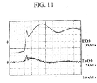
Figure 11 shows the impressed voltage waveform E(t) and current waveform I(t) in the
lighting circuit in figure 3 when the ringing voltage is lowered to 250 kHz.
Figure 12 is a diagram of the lighting waveform of another lamp.
Figure 13 is an enlarged view of the Z portion of figure 12, adding a calculated discharge
current waveform Id(t).
Figure 14 is a circuit diagram showing the constitution of another lighting circuit (push-pull).
Figure 15 is a waveform diagram to explain the operation of the lighting circuit in figure 14.
Figure 16 is a circuit diagram showing the constitution of a fly-back lighting circuit.
Figure 17 shows measured data for the impressed voltage waveform E(t) and current
waveform I(t) in a fly-back lighting circuit.
Figure 18 is a waveform diagram showing various values when a fly-back lighting circuit is
used.
Figure 19 is a diagram of a dielectric-barrier discharge lamp having two dielectrics pieces,
and of an equivalence circuit to illustrate the electrical operation.
Optimum Effect of Implementation of Invention
The mode of implementation of this invention is explained below.
Figure 3 is a circuit diagram showing one example of a lighting circuit for the dielectric-barrier
discharge lamp of an implementation of this invention; the figure shows a dielectric-barrier
discharge lamp lighting circuit that uses a full-bridge inverter circuit. In the figure, Lp
is the primary coil of the step-up transformer Tr, and D1 through D4 are diodes.
Figure 4 is a diagram that shows waveforms to explain the operation of the lighting circuit; it
is a model representation of the waveforms in a case where there is no primary or secondary
leakage inductance in the transformer, and the capacitive load continues without the discharge
phenomenon. In the drawing, Q1 through Q4 are switching elements (FET's, for example),
G1 through G4 are the gate signals of switching elements Q1 through Q4, Vp is the primary
voltage of the step-up transformer Tr (hereafter "transformer Tr"), and Vs is the voltage on
the secondary side of the transformer Tr.
The operation of the lighting circuit in figure 3 is explained by figure 4.
Figures 5 and 6 are measured data for the waveforms of the voltage impressed on the lamp
E(t) and the current I(t) in the circuit described above. Figure 6 is an enlarged view of the Y1
portion of figure 5; the waveforms were measured under the conditions mentioned below.
Now, these conditions are the conditions that most efficiently light the lighting circuit of
figure 3.
| Frequency: |
| Transformer Tr |
| Primary inductance: | 1.42 mH |
| Secondary inductance: | 204 mH |
| Coupling impedance: | .99955 |
| Dielectric-barrier discharge lamp |
| Dielectric: | quartz glass 1 mm thick |
| Discharge gas: | xenon at 33 kPa |
| Discharge gap: | 4.3 mm |
| Non-discharge static |
| capacitance of lamp: | 84 pF |
Figure 7 shows the waveform of the discharge current Id(t), the result of an analytical
calculation, in addition to the waveforms of the voltage impressed on the lamp E(t) and the
current I(t) shown in figures 5 and 6. It is an expanded view of portion Y2 of figure 6. The
following conditions are used in the analytical calculation:
| Static capacitance C1 of discharge plasma space: | 97.2 pF |
| Static capacitance C2 of dielectric: | 607 pF |
| Floating capacitance C3: | 70 pF |
The indentation at point K is clearly expressed in figure 7, and because the waveform of the
discharge current Id(t) is rising sharply at that point Td, it is knowing that indentation point K
is the beginning of the discharge. The time period from the indentation at point K to the first
subsequent peak P1 is τ, and the time period from the first peak P1 to the second peak P2 is
T12. Following the first peak P1, there is oscillation in the voltage impressed on the lamp
E(t).
In the lighting circuit of figure 3, the lighting efficiency is found by adding inductance to the
secondary side of the transformer Tr to adjust the ringing frequency (time period τ or time
period T12).
Figures 8, 9 and 10 show the relationship between the lighting efficiency η, found as
described above, and the time period τ, the time period T12 and the ringing frequency Fr.
Figure 11 shows the waveforms of the voltage impressed on the lamp E(t) and the discharge
current I(t) when the ringing frequency Fr is reduced to 250 Hz.
As is clear from figures 8, 9 and 10, making the time period τ no more than 2.1 µs, the time
period T12 no more than 3 µs, or the ringing frequency Fr at least 300 Hz is effective in terms
of increasing the efficiency. Now, the curves a, b and c in figures 8, 9 and 10 represent
efficiency in the event of changes in the voltage impressed on the lamp. The voltage
impressed on the lamp expressed by curve a is impressed voltage V1, curve b is impressed
voltage V2 and curve c is impressed voltage V3, such that V1 < V2 < V3. The relative
volumes of light in these cases are 1 for curve a, 1.33 for curve b and 1.67 for curve c.
Figure 12 shows measured data for the waveforms of the voltage impressed on the lamp E(t)
and the lamp current Is(t). The drawing shows an example of a case where there is no clear
voltage indentation at point K to indicate the beginning of discharge.
In a case where there is no clear indentation at point K, the point at which discharge begins
can be found by getting the waveform of the discharge current Id(t) from formula (1) above,
using the static capacitance C1 of the condenser 12 which is the discharge plasma space, the
static capacitance C2 of the condenser 13 which is the dielectrics 5,6, and the floating
capacitance C3 of the dielectric-barrier discharge lamp in parallel.
Figure 13 is an expanded view of portion Z of figure 12, and shows the analytical calculation
of the waveform of the discharge current Id(t) along with the waveforms of the voltage
impressed on the lamp E(t) and the lamp current Is(t). Now, the experimental conditions for
this drawing and for the analysis of the waveform of the discharge current Id(t) are as
follows:
| Power supply inverter method: | Push-pull |
| Static capacitance C1 of discharge plasma space: | 8.7 pF |
| Static capacitance C2 of dielectric: | 140 pF |
| Floating capacitance C3: | 10 pF |
The time Td seen in figure 13 marks the rapid rise of the discharge current Id(t), and is known
to be the beginning of discharge. Accordingly, the point on the waveform of the voltage
impressed on the lamp E(t) corresponding to this Td is equivalent to the indentation at point
K, and the time period τ can be found by measuring the time from the indentation at point K
to the next peak P1. In this example, the first peak P1 and the second peak P2 are clearly
expressed, and the time period T12 can be gotten from the waveform of the voltage impressed
on the lamp E(t).
Figure 14 is a diagram showing an example of the constitution using a push-pull inverter
circuit as the lighting circuit; figure 15 is a diagram of waveforms to explain the operation of
that lighting circuit. Figure 15 shows model waveforms for a case where there is no leakage
inductance on the primary or secondary sides of the transformer, and discharge does not occur
so the capacitive load is continuous. In the drawing, G1 and G2 are the gate signals of the
switching elements Q1 and Q2, V1 and V2 are voltages on the primary side of the
transformer Tr, and Vs is the voltage on the secondary side of the transformer Tr. The
operation of the lighting circuit of figure 3 is explained by figure 4.
As is clear from the explanation above, when a push-pull type inverter circuit is used as the
lighting circuit, the waveform of the voltage impressed on the dielectric-barrier discharge
lamp is almost the same as when a full-bridge type inverter is used. The time period τ, the
time period T12 and the ringing frequency Fr can all be found as described above. And
although it is not illustrated, it is the same with the use of a half-bridge inverter circuit.
Figure 16 is a diagram showing an example of the constitution using a fly-back inverter
circuit as the lighting circuit; figure 17 is a diagram of waveforms to explain the operation of
a fly-back inverter circuit as the lighting circuit.
As shown in figure 17, when a fly-back inverter circuit is used as the lighting circuit, the
waveforms of the voltage E(t) impressed on the dielectric-barrier discharge lamp and the
lamp current Is(t) are much different from those when a full-bridge, half-bridge or push-pull
inverter circuit is used. Nevertheless, it is possible to light the lamp with the same good
efficiency by focusing on the change of the waveform of the voltage impressed on the lamp
following the indentation at point K, even when using a fly-back type inverter circuit.
The following is an explanation of the case of lighting a dielectric-barrier discharge lamp
using a fly-back inverter circuit as the lighting circuit.
Figure 18 is a model diagram based on simulation of the waveforms in figure 17 and circuit
waveforms. In that drawing E(t) is the waveform of the voltage on the secondary side of the
transformer Tr in figure 16 (the voltage impressed on the dielectric-barrier discharge lamp);
Is(t) is the waveform of the lamp current; Id(t) is the discharge current waveform found by
analytical calculation; V.(t) is the waveform of the voltage on the switching element Q (an
FET, for example), Iq(t) is the waveform of the current through the switching element Q; Ir(t)
is the waveform of the current through the diode D1; ad G(t) is the gate signal input to the
gate driver circuit GD.
Figure 18 explains the operation of the lighting circuit shown in figure 17.
However, in the event that a diode D1 is connected in parallel with the switching element Q,
when the voltage V.(t) turns negative, there is a current flow through the diode D1 for time
period Tz from t3 to t4. This can be interpreted as a rapid reduction of the large impedance
on the primary side of the transformer. For that reason, the free resonant oscillation of the
voltage impressed on the lamp E(t) is obstructed, and in response there is a time period Tr
during which the change of voltage stops.
As above, in the case of a fly-back type lighting circuit, the waveform of the voltage
impressed on the lamp E(t) is relatively hard to understand, but the rise of the discharge
current Id(t) starts instant discharges at times Ta and Tb, and the indentation at point K can be
discriminated at that time.
In other words, even when using a fly-back type inverter circuit, it is possible to find a time
period τ from the indentation at point K, which indicates the beginning of discharge, to the
next peak. And it is possible to light the lamp with good efficiency by selecting an
inductance for the transformer Tr such that the time period τ will not exceed 2.1 µs.
Now, in the case of a fly-back type lighting circuit using a switching element Q with a reverse
parallel diode connected (or incorporating a reverse parallel diode), as described above, there
is a period Ts between the first peak P1 and the second peak P2 when the basically
unnecessary change of voltage stops. For that reason, the period T12 between the first and
second peaks is meaningless, and the relationship is not shown in figure 9.
In the event that the impedance of the circuit changes during operation, as above, attention is
required in the application of this invention. Now, in the case of a full-bridge, half-bridge,
push-pull or fly-back inverter circuit using a switching element to which a reverse parallel
diode has been added (or in which one has been incorporated), the problem described above
does not occur, since the primary side of the transformer is always connected to a power
supply with low impedance. Nevertheless, if the gate signal is turned OFF and the currently
flowing through the reverse parallel diode finally stops, the impedance thereafter is greater
and the voltage impressed on the lamp E(t) will begin resonant oscillation at a frequency
roughly determined by the static capacitance of the lamp and the inductance on the secondary
side, and the ringing will die away.
Now, it is possible that the discharge will not have been completed when the first peak is
passed, but in that event, the period T12 will be slightly longer than the period of subsequent
ringing. The extent to which it is longer will depend on the constitution of the lamp; that is,
on the distribution of the sizes of the static capacitance C1 of the condenser 12 which is the
discharge plasma space 2, and the static capacitance of the condenser 13 which is the
dielectrics 5, 6.
Even in such a case, it is desirable to constitute the light source equipment so as to fulfill the
specification T12 ≤ 3 µs, if possible.
If, on the other hand, it is not possible to fulfill the specification T12 ≤ 3 µs in such
circumstances, the discharge will generally grow weaker after the first peak has passed and
there will be little effect on the efficiency of ultraviolet light emission, and so it will be
sufficient to constitute the light source equipment so as to fulfill either the condition
LC ≤ 2.8 x 10⁻¹³ or the condition τ ≤ 2.1 µs.
Now, this invention can be applied both to dielectric-barrier discharge lamps that emit
ultraviolet light without a coating of fluorescent substance on the inner wall of the discharge
chamber and dielectric-barrier discharge lamps that emit visible light with a coating of
fluorescent substance on the inner wall of the discharge chamber.
In the invention explained above, it is possible to quickly cut off a discharge current that
would break down eximer molecules, and thus to improve the lighting efficiency of a
dielectric-barrier discharge lamp using a practical power supply, by constituting the lamp
such that (1) after passing the point in time when the voltage value to start a dielectric-barrier
discharge is reached, voltage is impressed on the dielectric-barrier discharge lamp for a
period of not more than 3 µs from the largest voltage value to the next largest voltage value;
or (2) voltage is impressed on the dielectric-barrier discharge lamp for a period of not more
than 2.1 µs from the voltage value at which the dielectric-barrier discharge commences until
the maximum voltage value in the next round of voltage impression; or (3) taking L as the
inductance and C as the static capacitance of the circuit comprising the power supply
equipment and the dielectric-barrier discharge lamp, the inductance L and static capacitance
C are selected to fulfill the formula LC ≤ 2.8 x 10⁻¹³.
Potential for Industrial Use
This invention is light source equipment that includes what is called a dielectric-barrier
discharge lamp, creating eximer molecules by means of a dielectric-barrier discharge and
using the light radiated from the eximer molecules; it can be used as an ultraviolet light
source for photochemical applications, for example.