FIELD OF THE INVENTION
-
The present invention relates to an interface circuit that
performs data transmission and reception between an external host
controller and a device connected to the external host controller.
BACKGROUND OF THE INVENTION
-
A conventional host interface circuit, which is mounted on a
device connected to an external host controller such as a
microcomputer, brings addresses in an internal storage space of
the connected device into one-to-one correspondence with
addresses in an internal storage space of the external host
controller. Therefore, when the external host controller reads
or writes data from/into the connected device, the external host
controller generates external addresses corresponding to the
respective internal addresses in the internal storage space of
the connected device, thereby performing data reading or writing.
-
Hereinafter, a description will be given of data
transmission/reception between a conventional external host
controller and a device connected to the external host controller,
with reference to figures 10 and 11.
-
Figure 10 is a block diagram illustrating an external host
controller 100 and a device 101 connected to the controller 100,
and figure 11 is a timing chart for explaining continuous access
to a series of areas in an internal storage space in the
connected device.
-
With reference to figure 10, the external host controller
100 includes a bus controller 102, and an internal storage space
104. The device 101 connected to the external host controller
100 includes a host interface circuit 103, and an internal
storage space 105.
-
Further, a chip selection signal 106, a read enable signal
107, and a write enable signal 108 are outputted from the
external host controller 100 to the host interface circuit 103 of
the connected device 101. An address bus 109 and a data bus 110
connect the external host controller 100 to the host interface
circuit 103 of the device 101. Further, 111 denotes an internal
operating clock of the connected device 101.
-
when the external host controller 100 so constructed reads
data stored in the internal storage space 105 of the connected
device 101, initially, the external host controller 100 generates
an external address corresponding to each of the internal
addresses 113 in the internal storage space 105 of the connected
device 101, a chip selection signal 106, and a read enable signal
107, which signals correspond to the external address. Then, the
host interface circuit 103 detects the falling edge of the read
enable signal 107 from the external host controller 100, in
synchronization with the internal operation clock 111 (112 in
figure 11). Thereby, the host interface circuit 103 judges that
the external host controller 100 makes access to the internal
storage space 105 of the connected device 101, and generates an
internal address 113 in the internal storage space 105
corresponding to the external address to perform reading of data.
-
For example, it is assumed that the external host controller
100 generates external addresses N, N+1, N+2, ... corresponding
to a series of areas in the internal storage space 105 of the
connected device 101, as shown in the timing chart of figure 11.
The host interface circuit 103 detects the falling edges of the
chip selection signal 106 and the read enable signal 107 (112 in
figure 11), which are supplied from the external host controller
100 operating on a clock different from the internal operation
clock 111, and judges that the external host controller 100 makes
access. Then, an address generation circuit in the connected
device 101 generates internal addresses s, s+1, s+2, ...
corresponding to the external addresses N, N+1, N+2, ...,
respectively, thereby performing continuous access to the serial
areas in the internal storage space 105.
-
Meanwhile, there is direct memory access (hereinafter
referred to as DMA) as another method of making continuous access
to a series of areas in the internal storage space of the device
connected to the external host controller. Figure 12 is a block
diagram illustrating a hardware structure performing DMA.
-
With reference to figure 12, DMA is direct data
transmission/reception between an external device connected to an
external host controller and a memory, without the intervention
of the external host controller. To perform DMA transfer,
setting on a DMA controller is carried out by software of the
external host controller through the following steps: (1) setting
a head address of a transfer data area on the memory, in a memory
address counter; (2) setting the number of words to be
transferred, in a number-of-words counter; (3) setting either
"reading" or "writing" in a control register in a control
circuit; (4) making a transfer start instruction.
-
After the above-described setting, the DMA controller
increments the memory address counter while decrementing the
number-of-words counter until the count of the number-of-words
counter becomes 0, thereby making continuous access to a series
of areas in the internal storage space of the external device
connected to the external host controller.
-
Since, in DMA, the external host controller doesn't need to
directly control data transmission/reception, the load on the
external host controller is not so great. However, it is
necessary to make interruption to the external host controller
when DMA transfer is ended. Further, since the external host
controller and the DMA controller basically operate independently
from each other, there is a possibility of competition for memory
access. Therefore, DMA requires a memory bus controller to
arbitrate competition for memory access between the external host
controller and the DMA controller.
-
As described above, when performing data transmission/
reception between the external host controller and the device
connected to the external host controller by using the
conventional host interface circuit, the addresses corresponding
to the internal storage space of the external host controller are
brought into one-to-one correspondence with the addresses
corresponding to the internal storage space of the connected
device. Therefore, when the external host controller makes
continuous access to a series of areas-in the internal storage
space in the connected device, the external host controller must
generate individual external addresses corresponding to the
respective internal addresses in the internal storage space of
the connected device. Accordingly, signal transition occurs on
the external address bus every time access is made to the
internal address in the internal storage space of the connected
device, resulting in power consumption due to the signal
transition on the external address bus.
-
Further, when performing transmission/reception of plural
data streams between the external host controller and the device
connected to the external host controller, the external host
controller must generate and manage external addresses
corresponding to the internal storage space of the connected
device, for every data stream to be transmitted/received, to make
access to the connected device. Therefore, the processing by
software of the external host controller is complicated.
-
On the other hand, although continuous access to a series of
areas by DMA is efficient, since special DMA controller and
memory bus controller are required in addition to the
conventional bus controller and interface circuit, the hardware
scale is increased. Further, since interruption or the like is
required, the software processing is complicated.
-
Accordingly, if the external host controller has processing
ability enough and to spare, it might be better not to use DMA.
However, as mentioned above, the conventional host interface
circuit has the problem of power consumption due to the signal
transition on the external address bus.
SUMMARY OF THE INVENTION
-
The present invention is made to solve the above-described-problems
and has for its object to provide a host interface
circuit that performs data transmission/reception via a bus
controller circuit of an external host controller, without the
need for a DMA controller and a memory bus controller, and that
significantly reduces signal transitions on the external address
bus to reduce the power consumption, and prevents the software
processing of the external host controller from being complicated.
-
Other objects and advantages of the invention will become
apparent from the detailed description that follows. The
detailed description and specific embodiments described are
provided only for illustration since various additions and
modifications within the scope of the invention will be apparent
to those of skill in the art from the detailed description.
-
According to a first aspect of the present invention, there
is provided a host interface circuit performing data
transmission/reception between an external host controller and a
device connected to the external host controller in such a manner
that each address and data to be transmitted/received is
accompanied with a chip selection signal indicating that the
external host controller makes access to the device connected to
the external host controller, and a read enable signal or a write
enable signal, wherein the external host controller generates, as
external addresses to be supplied to the device connected to the
external host controller, first addresses corresponding to the
respective internal addresses in an internal storage space of the
device connected to the external host controller, and a specific
second address corresponding to internal addresses of a series of
areas in the internal storage space; the host interface circuit
includes a first address conversion circuit for converting the
first addresses into the internal addresses in the internal
storage space, and a second address conversion circuit for
converting the specific second address into the internal
addresses in the internal storage space; and the specific second
address is used when the external host controller makes
continuous access to the serial areas in the internal storage
space of the device connected to the external host controller.
Therefore, when the external host controller makes continuous
access to a series of areas in the internal storage space of the
device connected to the controller, continuous access to the
areas in the internal storage space of the connected device is
achieved using the specific address, without using DMA, between
the external host controller and the host interface circuit. As
the result, power consumption is reduced, and complexity in
software processing is reduced.
-
According to a second aspect of the present invention, in
the host interface circuit according to the first aspect, the
external host controller generates a plurality of specific second
addresses corresponding to different kinds of data to be
transmitted/received, respectively, as external addresses to be
supplied to the device connected to the external host controller;
and the host interface circuit includes a plurality of second
address conversion circuits corresponding to the respective
specific second addresses. Therefore, when the external host
controller makes continuous access to a series of areas in the
internal storage space of the device connected to the controller,
the external host controller can properly use a specific address
for each of plural data streams to be transmitted/received
between the external host controller and the device connected to
the controller, whereby complexity in software processing on the
plural data streams is reduced.
-
According to a third aspect of the present invention, in the
host interface circuit according to the first aspect, the second
address conversion circuit is provided with plural kinds of
address generation methods for generating the internal addresses
in the internal storage space corresponding to the specific
second address, and generates the internal addresses
corresponding to the specific second address by using any of the
address generation methods according to setting of the external
host controller. Since the external host controller specifies
the address generation method, the external host controller can
control the order of continuous access to a series of areas in
the internal storage space of the device connected to the
controller, whereby power consumption due to signal transition on
an external address bus is reduced, and complexity in software
processing in the external host controller is reduced.
-
According to a fourth aspect of the present invention, in
the host interface circuit according to the second aspect, each
of said second address conversion circuits is provided with
plural kinds of address generation methods for generating the
internal addresses in the internal storage space corresponding to
the specific second address, and generates the internal addresses
corresponding to the specific second address by using any of the
address generation methods according to setting of the external
host controller. Since the external host controller specifies
the address generation method, the external host controller can
control the order of continuous access to a series of areas in
the internal storage space of the device connected to the
controller, whereby power consumption due to signal transition in
an external address bus is reduced, and complexity in software
processing in the external host controller is reduced.
-
According to a fifth aspect of the present invention, in the
host interface circuit according to any of the first to fourth
aspects, the host interface circuit further includes a register
for setting an access cycle to a control signal which
continuously asserts the read enable signal or the write enable
signal during continuous transmission/reception of plural data by
the external host controller, and a control circuit for
controlling reading or writing of data from/into the internal
storage space, according to the value set in the register; and
when the external host controller continuously performs
transmission/reception of plural pieces of data using the second
address, with the device connected to the external host
controller, the host interface circuit performs, under control of
the control circuit, reading or writing of the respective data
from the internal addresses generated by the second address
conversion circuit. Therefore, the respective data, which are
continuously transmitted/received using the specific address, can
be read or written from/into the respective addresses in the
internal storage space, whereby power consumption is reduced.
BRIEF DESCRIPTION OF THE DRAWINGS
-
- Figure 1 is a block diagram illustrating the hardware
structure of a host interface circuit according to a first
embodiment of the present invention.
- Figure 2 is a timing chart for explaining data
transmission/reception between the host interface circuit
according to the first embodiment and an external host controller.
- Figure 3 is a block diagram illustrating the hardware
structure of a host interface circuit according to a second
embodiment of the present invention.
- Figures 4(a) and 4(b) are diagrams illustrating, when
transmitting/receiving data streams using specific external
addresses (second addresses), allocation of storage areas in an
internal storage space of a video coding/decoding apparatus where
the transmitted/received data are stored.
- Figure 5 is a block diagram illustrating the hardware
structure of a host interface circuit according to a third
embodiment of the present invention.
- Figures 6 (a) and 6 (b) are diagrams for explaining data
storage positions when two-dimensional array data are stored in
an internal storage space that is a one-dimensional array.
- Figure 7 is a timing chart for explaining data
transmission/reception between the host interface circuit
according to the third embodiment and an external host controller.
- Figure 8 is a block diagram illustrating the hardware
structure of a host interface circuit according to a fourth
embodiment of the present invention.
- Figure 9 is a timing chart for explaining data
transmission/reception between the host interface circuit of the
fourth embodiment and an external host controller.
- Figure 10 is a block diagram illustrating the structure of a
conventional host interface circuit.
- Figure 11 is a timing chart for explaining the manner of
making continuous access to a series of areas in an internal
storage space of a device connected to an external host
controller, using the conventional host interface circuit.
- Figure 12 is a block diagram illustrating a hardware
structure for explaining conventional direct memory access.
-
DETAILED DESCRIPTION OF THE PREFERRED EMBODIMENTS
-
Hereinafter, the preferred embodiments of the present
invention will be described with reference to the drawings. The
embodiments of the present invention employs, as a device
connected to an external host controller, a video coding/decoding
apparatus that requires transmission/reception of a large amount
of data such as coded video data.
[Embodiment 1]
-
Hereinafter, a first embodiment of the present invention
will be described.
-
First of all, the structure of a host interface circuit
according to the first embodiment of the invention will be
described with reference to figure 1.
-
Figure 1 is a block diagram illustrating the hardware
structure of a host interface circuit 103 according to the first
embodiment. In figure 1, 101 denotes a video coding/decoding
apparatus connected to an external host controller (not shown),
and contains the host interface circuit 103. Further, the video
coding/decoding apparatus 101 is provided with an internal
storage space 105. The host interface circuit 103 and the
external host controller are connected through a chip selection
signal 106, a read enable signal 107, a write enable signal 108,
an address bus 109, and a data bus 110.
-
The host interface circuit 103 is provided with a
synchronization circuit 200, a read/write control circuit 201,
and an address generation circuit 204. The synchronization
circuit 200 synchronizes a signal from the external host
controller which operates asynchronously with the video
coding/decoding apparatus 101, with an internal operation clock
111. The read/write control circuit 201 generates an internal
read signal 202 and an internal write signal 203 to an internal
storage space 105. The address generation circuit 204 generates
internal addresses corresponding to the internal storage space
105, from external addresses supplied from the external host
controller.
-
The address generation circuit 204 comprises a first address
conversion circuit 205, a second address conversion circuit 206,
and an selection circuit 207. The first address conversion
circuit 205 converts the respective external addresses (first
addresses) in an internal storage space of the external host
controller into internal addresses 113 in the internal storage
space 105 of the video coding/decoding apparatus 101 so that the
internal addresses 113 are in one-to-one correspondence with the
external addresses (first addresses). The second address
conversion circuit 206 converts a specific external address (a
second address) for making continuous access to a series of areas
in the internal storage space 105 into internal addresses 113.
The selection circuit 207 selects either the first address
conversion circuit 205 or the second address conversion circuit
206, according to the external address supplied from the external
host controller.
-
Next, the operation of the host interface circuit 103
according to the first embodiment will be described with
reference to figure 2, with respect to the case where the
external host controller transmits coded video data to the video
coding/decoding apparatus 101, and the case where the external
host controller receives coded video data from the video
coding/decoding apparatus 101.
-
Figure 2 is a timing chart for explaining data
transmission/reception between the external host controller and
the video coding/decoding apparatus 101 containing the host
interface circuit 103.
-
Initially, a description will be given of the case where the
external host controller transmits coded video data to the video
coding/decoding apparatus 101.
-
The external host controller generates external addresses
(first addresses) corresponding to the respective internal
addresses in the internal storage space 105 of the video
coding/decoding apparatus 101 that is connected to the external
host controller, and writes control commands such as the type of
data to transmit, the data size, and the like, into the internal
addresses in the internal storage space 105 corresponding to the
external addresses.
-
Then, the external host controller sets a head address s of
an area in the internal storage space 105 of the video
coding/decoding apparatus 101, where coded video data transmitted
from the external host controller are to be written, on an
address pointer 208 in the second address conversion circuit 206.
Thereafter, the external host controller transmits a specific
external address (a second address) M corresponding to the coded
video data to transmit, together with the chip selection signal
106 and the write enable signal 108, through the address bus 109,
to the video coding/decoding apparatus 101. Then, as shown in
the timing chart of figure 2, the specific external address
(second address) M is converted into the corresponding internal
addresses 113 by the second address conversion circuit 206, and
the coded video data are written in the internal storage area
assigned by the internal addresses 113.
-
Further, the read/write control circuit 201 in the host
interface circuit 103 detects the falling edges of the chip
selection signal 106 and the write enable signal 108 from the
external host controller, in synchronization with the internal
operation clock 111 (112 in figure 2), thereby judging that the
external host controller performs writing of data. When the
external address given to the address bus 109 at this time is the
specific address (second address) M for making continuous access
to a series of areas in the internal storage space 105 of the
video coding/decoding apparatus 101, the second address
conversion circuit 206 is selected by the selection circuit 207,
and the address value (s, s+1, ..., s+m-1, s+m) outputted from
the address pointer 208 is selected as the internal address 113
of the internal storage space 105, and the data transmitted from
the external host controller is written in this address and,
further, the value of the address pointer is incremented by 1.
This operation is repeated for the amount of data to be
transmitted from the external host controller as shown in figure
2.
-
Next, a description will be given of the case where the
external host controller receives coded video data from the video
coding/decoding apparatus 101.
-
The external host controller generates external addresses
(first addresses) corresponding to the respective internal
addresses in the internal storage space 105 of the video
coding/decoding apparatus 101 that is connected to the controller,
and writes control commands such as the type of data to receive,
the data size, and the like, into the internal addresses in the
internal storage space 105 corresponding to the external
addresses (first addresses).
-
The video coding/decoding apparatus 101 makes preparation
for transmission of coded video data to the external host
controller, according to the control commands transmitted from
the external host controller. When the preparation has been made,
the video coding/decoding apparatus 101 notifies it to the
external host controller. This notification is carried out by
interruption to the external host controller, or polling to a
status register from the external host controller.
-
On receipt of the notification, the external host controller
sets a head address s of an area in the internal storage space
105 where the coded video data to receive are stored, on the
address pointer 208 in the second address conversion circuit 206.
Thereafter, the external host controller transmits the specific
external address (second address) M corresponding to the coded
video data to receive, together with the chip selection signal
106 and the read enable signal 107, through the address bus 109,
to the video coding/decoding apparatus 101. Then, as shown in
the timing chart of figure 2, the specific external address
(second address) M is converted into the corresponding internal
addresses 113 by the second address conversion circuit 206, and
the coded video data are read from the internal addresses.
-
Further, the read/write control circuit 201 in the host
interface circuit 103 detects the falling edges of the chip
selection signal 106 and the write enable signal 108 from the
external host controller, in synchronization with the internal
operation clock 111, thereby judging that the external host
controller performs reading of data. When the external address
given to the address bus 109 at this time is the specific address
(second address) M for making continuous access to a series of
areas in the internal storage space 105 of the video
coding/decoding apparatus 101, the second address conversion
circuit 206 is selected by the selection circuit 207, and the
address value (s, s+1, ..., s+m-1, s+m) outputted from the
address pointer 208 is selected as the internal address 113, and
the corresponding data is read from the internal storage space
105 to be transmitted to the external host controller and,
further, the value of the address pointer is incremented by 1.
This operation is repeated for the amount of data to be received
by the external host controller as shown in figure 2.
-
When making continuous access to a series of areas in the
internal storage space 105 of the video coding/decoding apparatus
101 by using the specific external address (second address) M,
the access size m is determined considering the capacity of the
physical storage space that is contained in the video
coding/decoding apparatus 101.
-
When performing data transmission/reception between the
external host controller and the video coding/decoding apparatus
101, data are usually transmitted/received in units of
predetermined number of bytes. For example, assuming that coded
video data are transmitted/received in units of 256 bytes, signal
transitions occur in the lower 8 bits of the external address bus
109 in the conventional host interface circuit. To be specific,
in each signal line of the external address bus 109, low-to-high
signal transitions and high-to-low signal transitions occur 256
times at the 0th bit, 128 times at the 1st bit, 64 times at the
2nd bit, 32 times at the 3rd bit, 16 times at the 4th bit, 8
times at the 5th bit, 4 times at the 6th bit, and 2 times at the
7th bit. However, in the host interface circuit 103 according to
the first embodiment, since the specific external address (second
address) is used when coded video data are transmitted in units
of predetermined number of bytes, such signal transition hardly
occurs.
-
Further, in general, a power Pd that is consumed by charging
and discharging due to signal transition is represented by the
following formula.
Pd = α · C · fp · V · V
wherein α is the signal transition rate, C is the load capacity
to be driven, fp is the operating frequency, and V is the power
supply voltage. It can be seen from formula (1) that the power
Pd consumed by charging and discharging due to signal transition
increases in proportion to the signal transition rate α and the
load capacity C when the operating frequency fp and the power
supply voltage V are constant. That is, the power Pd can be
reduced by reducing the signal transitions on the external
address bus.
-
Accordingly, in the host interface circuit 103 according to
the first embodiment, the power consumption can be significantly
reduced as compared with that in the conventional host interface
circuit.
-
In this first embodiment, since the host interface circuit
103 includes the second address conversion circuit 206 for
generating addresses in the internal storage space 105
corresponding to the specific external address (second address),
the power consumption inside the video coding/decoding apparatus
101 is larger than that in the conventional device. however,
since the host interface circuit 103 is in an LSI, and the power
required to drive the gates in the LSI is only several µW order
while the power required to drive an external device having a
large load capacity is several mW order. Therefore, if the
signal transitions on the external address bus 109 can be
significantly reduced, the power consumption of the LSI as a
whole can be reduced.
-
According to the first embodiment of the invention, when the
host interface circuit 103 performs continuous transmission/
reception of coded video data between the external host
controller and the video coding/decoding apparatus 101, the host
interface circuit 103 uses the specific address (second address)
M for making continuous access to a series of areas in the
internal storage space 105 of the video coding/decoding apparatus
101, whereby signal transitions on the external address bus 109
are significantly reduced. Further, since DMA is not used for
making continuous access to a series of areas in the internal
storage space 105, the hardware scale is prevented from
increasing, and the software processing of the external host
controller is prevented from being complicated.
[Embodiment 2]
-
Hereinafter, a second embodiment of the present invention
will be described.
-
A host interface circuit according to the second embodiment
is further provided with means for simplifying the software
processing of the external host controller when
transmittinq/receiving plural pieces of coded video data, or
different kinds of data such as coded video data and coded audio
data.
-
First of all, the structure of a host interface circuit
according to the second embodiment will be described with
reference to figure 3.
-
Figure 3 is a block diagram illustrating the hardware
structure of a host interface circuit 103 according to the second
embodiment. In figure 3, the same reference numerals as those
shown in figure 1 designate the same or corresponding parts.
-
With reference to figure 3, in the host interface circuit
103, an address generation circuit 206a is provided with two
address pointers A208 and B209, and the external host controller
generates two specific addresses M0 and M1 (second addresses)
used for continuous access to a series of areas in the internal
storage space 105 of the video coding/decoding apparatus 101 that
is connected to the external host controller. The external
addresses M0 and M1 correspond to the address pointers A208 and
B209, respectively.
-
Hereinafter, a description will be given of the access size
when making, using the specific external addresses M0 and M1,
continuous access to a series of areas in the internal storage
space 105 of the video coding/decoding apparatus 101 connected to
the external host controller.
-
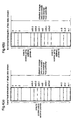
Figures 4(a) and 4(b) are diagram for explaining allocation
of storage areas in the internal storage space 105 of the video
coding/decoding apparatus 101, where data to be transmitted/
received are stored. To be specific, figure 4(a) shows
allocation of storage areas in the internal storage space when a
single (one kind of) data stream is transmitted/received, and
figure 4(b) shows allocation of storage areas in the internal
storage space when plural (two kinds of) data streams are
transmitted/received. In this second embodiment, for
transmission/reception of two data streams, the internal storage
space 105 is evenly allocated to the two data streams to be
transmitted/received.
-
Assuming that the physical storage space in the video
coding/decoding apparatus 101 connected to the external host
controller has a capacity of m bytes, a data stream of m bytes
can be transmitted/received at one time by using the specific
external address (second address) M as shown in figure 4(a), and
a data stream of m/2 bytes can be transmitted/received at one
time by using the specific external address (second address) M0
or M1 as shown in figure 4(b).
-
It is now assumed that, until the external host controller
has transmitted a data stream, the video coding/decoding
apparatus 101 does not perform processing on the received data
stream. Under this assumption, when a data stream more than m
bytes (figure 4(a)) or a data stream more than m/2 bytes (figure
4(b)) is transmitted from the external host controller to the
video coding/decoding apparatus 101, the transmitted data stream
overwrites the data stream stored in the video coding/decoding
apparatus 101 before the stored data stream is processed.
Therefore, in the software processing of the external host
controller, data transmission/reception should be carried out
considering the capacity of the physical storage space contained
in the video coding/decoding apparatus 101 that is accessible
from the external host controller.
-
To be specific, when making continuous access to a series of
areas in the internal storage space 105 of the video
coding/decoding apparatus by using the specific external address
M or the specific external addresses M0 and M1, the access size m
is determined considering the capacity of the physical storage
space contained in the video coding/decoding apparatus 101.
-
Next, the operation of the host interface circuit according
to the second embodiment will be described.
-
In the host interface circuit 103, the read/write control
circuit 201 detects the falling edges of the chip selection
signal 106 and the read enable signal 107 or the write enable
signal 108 supplied from the external host controller, in
synchronization with the internal operation clock 111, thereby
judging that the external host controller performs data reading
or writing. At this time, when the external address given to the
address bus 109 is the specific external address (second address)
M0 or M1 for making continuous access to a series of areas in the
internal storage space 105, the selection circuit 207 selects the
address pointer A208 or B209 as the internal address 113 of the
internal storage space 105, and data is written in the internal
storage space 105 or read from the space 105 to be outputted to
the external host controller and, simultaneously, the value of
the address pointer A208 or B209 corresponding to the specific
external address M0 or M1, respectively, is incremented by 1.
This operation is repeated for the amount of data to be
transmitted/received by the external host controller, as
described for the first embodiment.
-
when the internal storage space 105 of the video
coding/decoding apparatus 101 is evenly allocated to accesses by
the specific external addresses (second addresses) M0 and M1, the
host interface circuit 103 makes access to the internal address
areas of s, s+1, s+2, ..., s+m/2-1 by the address pointer A208
when the specific external address is M0. On the other hand, the
host interface circuit 103 makes access to the internal address
areas of s+m/2, s+m/2+1, s+m/2+2, ..., s+m by the address pointer
B209 when the specific external address is M1.
-
The host interface circuit 103 of this second embodiment is
applicable to MPEG4 that is the international standard of video
coding. In MPEG4, an image displayed on a screen is composed of
plural objects, and the respective objects constituting the image
are coded separately. Accordingly, plural pieces of coded video
data are transmitted/received between the video coding/decoding
apparatus 101 and the external host controller.
-
Therefore, when there is only one set of a specific external
address (second address) and an address pointer for making
continuous access to a series of areas in the internal storage
space 105, in order to transmit/receive the plural pieces of
coded video data, the external host controller must set the head
address of coded video data to be transmitted/received every time
transmission/reception of the coded video data is started and,
moreover, the external host controller must store the storage
addresses of the coded video data to be transmitted/received,
resulting in complicated software processing of the external host
controller. In order to solve this problem, the plural pieces of
coded video data are provided with the specific external
addresses (second addresses), respectively, and the host
interface circuit 103 is provided with the address pointers
corresponding to the respective external addresses, whereby the
software processing of the external host controller is prevented
from being complicated.
-
As described above, according to the second embodiment of
the invention, the host interface circuit 103 can reduce the
power consumption due to signal transition, as described for the
first embodiment. Moreover, since the host interface circuit 103
uses the specific external addresses (second addresses)
corresponding to different kinds of coded streams, and the
address pointers corresponding to the respective external
addresses, the software processing of the external host
controller can dispense with setting of a head address of coded
video data every time transmission/reception of coded video data
is started, and storage of addresses of coded image data to be
transmitted/received. As the result, the software processing of
the external host controller is prevented from being complicated.
-
While in the second embodiment the second address conversion
circuit 206a generates two specific external addresses (second
addresses) and is provided with two address pointers
corresponding to the respective external addresses, the number of
the specific external addresses and the address pointers is not
restricted to two.
[Embodiment 3]
-
Hereinafter, a description will be given of a third
embodiment of the present invention.
-
A host interface circuit of this third embodiment is further
provided with means for simplifying the software processing of
the external host controller, when making access to the internal
storage space 105 in the video coding/decoding apparatus 101
connected to the external host controller, by using a specific
address (second address) for making continuous access to a series
of areas in the internal storage space 105.
-
Initially, the structure of the host interface circuit
according to the third embodiment will be described with
reference to figure 5.
-
Figure 5 is a block diagram illustrating the hardware
structure of a host interface circuit 103 according to the third
embodiment. In figure 5, the same reference numerals as those
shown in figure 1 denote the same or corresponding parts.
-
In the host interface circuit 103 shown in figure 5, when a
series of areas in the internal storage space 105 of the video
coding/decoding apparatus 101 connected to the external host
controller are continuously accessed by using a specific external
address (second address), the address pointer A208 in the second
address conversion circuit 206b for generating internal addresses
113 of the internal storage space 105 from the specific external
address (second address) is provided with an address generation
control circuit 210 for controlling address generation. Further,
the address generation control circuit 210 includes an index
register A211.
-
Next, the operation of the host interface circuit 103
according to the third embodiment will be described with
reference to figures 6 and 7. In this third embodiment, access
to two-dimensional array data is taken as an example.
-
Figures 6(a) and 6(b) are diagrams illustrating data storage
positions when two-dimensional array data (figure 6(a)) are
stored in the internal storage space 105 that is a one-dimensional
array (figure 6(b)). Figure 7 is a timing chart for
explaining data transmission/reception between the video
coding/decoding apparatus containing the host interface circuit
103 and the external host controller.
-
In the host interface circuit 103, the address generation
control circuit 210 prepares a plurality of address generation
methods for generating addresses in the internal storage space
105, and the falling edges (112 in figure 7) of the chip
selection signal 106 and the read enable signal 107 or the write
enable signal 108 supplied from the external host controller are
detected in synchronization with the internal operation clock 111
to judge that the external host controller performs data reading
or writing. When the external address given to the address bus
109 at this time is the specific address (second address) M0 for
making continuous access to a series of areas in the internal
storage space 105, the address generation control circuit 210
generates internal addresses 113 to the address pointer A208,
according to an address generation method designated by the
external host controller.
-
When the external host controller makes continuous access to
a series of areas in the column direction of the two-dimensional
array data stored in the internal storage space 105, the external
host controller can use the specific address (second address) M0
for continuous access to the serial areas in the internal storage
space 105, as described for the first and second embodiments.
-
However, when the external host controller makes continuous
access to a series of areas in the row direction of the two-dimensional
array data, the external host controller cannot make
continuous access to the serial areas in the internal storage
space 105 by using the specific address (second address) M0 in
the method where the address pointer A208 for generating the
internal addresses 113 is one by one incremented for every
specific address (second address) M0.
-
For example, with reference to figures 6(a) and 6(b), when
the external host controller makes continuous access to the two-dimensional
array data in the row direction by using the specific
address (second address) M0, the address pointer A208 for
generating the internal addresses 113 must be incremented by t at
a time.
-
Accordingly, when data are arranged in two-dimensional array
as shown in figure 6(a), since the host interface circuit 103
according to the first or second embodiment cannot make
continuous access to the serial areas in the internal storage
space 105 by using the specific address (second address) M0, the
external host controller must generate, for continuous access,
plural external addresses (first addresses) in one-to-one
correspondence with the internal addresses in the internal
storage space 105. That is, every time the external host
controller makes access to the internal address in the storage
space 105, the controller must generate the corresponding
external address, resulting in power consumption due to signal
transition of the external address.
-
In order to solve this problem, in this third embodiment,
the address generation control circuit 210 is provided with the
index register A211 as shown in figure 5, and the address
generation control circuit 210 generates plural kinds of methods
of updating the address pointer A208 with respect to the specific
address (second address) M0 for making continuous access to the
serial areas in the internal storage space 105, i.e., plural
kinds of access orders to the internal storage space 105. The
access orders are set by the external host controller.
-
When the external host controller makes access to the
internal storage space 105 in the column direction of the two-dimensional
array data shown in figure 6(a), a head address s for
making access to the internal storage space 105 is set in the
address pointer A208 shown in figure 5, and t is set in the index
register A211 as a value to update the address pointer A208, as
shown in the timing chart of figure 7. The address generation
control circuit 210 updates the address pointer A208 by the value
t that is set in the index register A211, at every access using
the specific address (second address) M0, whereby the address
pointer A208 is updated like s, s+t, s+2t, ... In this way,
continuous access to D(0,0), D(1,0), D(2,0), ... is achieved
using the specific address (second address) M0, in the row
direction of the two-dimensional array data shown in figure 6(a).
-
Furthermore, when using the above-mentioned access method,
setting of the head address s for initial access and the index
value t is all that is required of the external host controller,
and the external host controller doesn't need to perform the
process of updating the external address at every access.
-
As described above, according to the third embodiment of the
invention, the host interface circuit 103 is further provided
with the address generation control circuit 210, and the address
generation control circuit 210 provides plural kinds of address
generation methods for generating addresses in the internal
storage space 105 of the video coding/decoding apparatus 101,
with respect to access using the specific external address
(second address). Thereby, it is possible to make continuous
access to a series of areas in the internal storage space 105
using the specific external address (second address) with respect
to plural access modes performed by the external host controller.
As the result, power consumption due to signal transition on the
external address bus is reduced as described for the first
embodiment and, moreover, the software processing of the external
host controller is prevented from being complicated.
-
While in this third embodiment the second address conversion
circuit 206b is provided with one address pointer and one address
generation circuit including an index register, when plural kinds
of data, such as still-picture data and video data, are handled
and thereby plural pieces of specific external addresses (second
addresses) are provided, the second address conversion circuit
206b is provided with plural address pointers and plural address
generation circuits as many as the external addresses.
[Embodiment 4]
-
Hereinafter, a fourth embodiment of the present invention
will be described.
-
In this fourth embodiment, a host interface circuit
according to any of the first to third embodiments is modified to
realize reading or writing of data from/into the internal storage
space of the external host controller, in the case where, as
shown in figure 9, the chip selection signal 106 and the read
enable signal 107 or the write enable signal 108 supplied from
the external host controller are continuously asserted with
respect to continuous data reading or writing.
-
Figure 9 is a timing chart for explaining data
transmission/reception between the video coding/decoding
apparatus 101 containing the host interface circuit of this
fourth embodiment, and the external host controller.
-
In the case where the external host controller and the video
coding/decoding apparatus 101 connected to the host controller
operate on different clocks, when the read enable signal 107 or
the write enable signal 108 is asserted before starting reading
or writing of each address and data and is negated when the
reading or writing is ended as shown in the timing chart of
figure 2 described for the first embodiment, the host interface
circuit 103 in the video coding/decoding apparatus 101 detects
the falling edges of the chip selection signal 106 and the read
enable signal 107 in synchronization with the internal operation
clock 111 (112 in figure 2) to judge that reading of data from
the internal storage space 105 is carried out and, furthermore,
the host interface circuit 103 detects the falling edges of the
chip selection signal 106 and the write enable signal 108 (112 in
figure 2) to judge that writing of data into the internal storage
space 105 is carried out.
-
However, as shown in the timing chart of figure 9, when the
read enable signal 107 or the write enable signal 108 is
continuously asserted with respect to continuous reading or
writing of plural addresses and data fram/into the external host
controller, even if the falling edges of the chip selection
signal 106 and the read enable signal 107 or the write enable
signal 108 are detected in synchronization with the internal
operation clock 111, the boundaries of addresses and the
boundaries of data cannot be detected in the continuously
carried-out reading or writing of the addresses and data.
-
In the conventional access method using the external
addresses in one-to-one correspondence with the internal
addresses, the boundaries of addresses or data can be detected as
the external address varies. However, when using the specific
address (second address) for making continuous access to a series
of areas in the internal storage space 105 of the video
coding/decoding apparatus 101 connected to the external host
controller as described for the first to third embodiments, the
boundaries of addresses or data cannot be detected as the
external address does not vary.
-
Hereinafter, the structure of the host interface circuit 103
according to this fourth embodiment will be described with
reference to figure 8.
-
Figure 8 is a block diagram illustrating the hardware
structure of the host interface circuit 103 according to the
fourth embodiment. In figure 8, the same reference numerals as
those shown in figure 1 denote the same or corresponding parts.
-
In figure 8, a read/write control circuit 201a is provided
with a read/write control counter 300 for controlling
reading/writing of data from/into the internal storage space 105,
and a cycle setting register 301 for setting the number of
read/write cycles, in addition to a circuit for detecting falling
edges (112 in figure 9) and rising edges (114 in figure 9) of the
chip selection signal 106, the read enable signal 107, and the
write enable signal 108, in synchronization with the internal
operation clock 111.
-
Next, the operation of the host interface circuit 103
according to the fourth embodiment will be described with
reference to figures 2 and 9.
-
Initially, the read/write control counter 300 in the
read/write control circuit 201a sets the count at 0 when it is
reset. Next, in advance of reading or writing of data from/into
the internal storage space 105, the external host controller sets
a predetermined value in the cycle setting register 301, on the
basis of the number of cycles required for reading or writing of
data from/into the internal storage space 105 or the number of
waits in the bus interface circuit of the external host
controller, at timings of dropping the chip selection signal 106
and the read enable signal 107 or the write enable signal 108 for
reading or writing one address and data, and raising these
signals after performing reading or writing, as shown in the
timing chart of figure 2 described for the first embodiment. In
this fourth embodiment, the external host controller sets "5" in
the cycle setting register 301.
-
Then, the read/write control circuit 201a detects, in
synchronization with the internal operation clock 111, the
falling edges of the chip selection signal 106 and the read
enable signal 107 or the write enable signal 108, which are
supplied from the external host controller that operates on a
clock different from the internal operation clock 111, and the
read/write control counter 300 starts counting at the timing when
the falling edges of these signals are detected.
-
When the count of the read/write control counter 300 is "1"
or "2", the synchronization circuit 200 samples the values of the
external address and data which are given to the address bus 109
and the data bus 110 in synchronization with the internal
operation clock 111, and when the count becomes "3", the
read/write control circuit 201a generates an internal read signal
202 or an internal write signal 203 to the internal storage space
105, whereby reading or writing of data from the internal storage
space 105 is carried out. This operation is repeated while the
chip selection signal 106 and the read enable signal 107 or the
write enable signal 108 are being asserted.
-
Then, the read/write control counter 300 resets the count to
"0" to stop counting at the timing when the rising edges of the
chip selection signal 106 and the read enable signal 107 or the
write enable signal 108 are detected (114 in figure 9).
-
As described above, according to the fourth embodiment of
the invention, since the host interface circuit 103 is provided
with the read/write control circuit 300 and the cycle setting
register 301, even when the read enable signal 107 or the write
enable signal 108 is continuously asserted for continuous reading
or writing of plural addresses and data from/into the external
host controller, continuous reading or writing from/into a series
of areas in the internal storage space 105 of the video
coding/decoding apparatus 101 can be carried out using the
specific address (second address). Thereby, signal transitions
on the external address bus in the host interface circuit 103 are
significantly reduced, resulting in reduced power consumption.
-
While in the first to fourth embodiments of the invention
the read/write control circuit 201 (or 201a) detects the falling
edges of the chip selection signal 106 and the read enable signal
107 (or the write enable signal 108) supplied from the external
host controller, the read/write control circuit 201 (or 201a) may
detect the rising edges of these signals, depending on the
polarity (positive logic, negative logic) of the read enable
signal 107 or the write enable signal 108.