EP1104092A2 - Operational amplifier with digital offset calibration - Google Patents
Operational amplifier with digital offset calibration Download PDFInfo
- Publication number
- EP1104092A2 EP1104092A2 EP00118854A EP00118854A EP1104092A2 EP 1104092 A2 EP1104092 A2 EP 1104092A2 EP 00118854 A EP00118854 A EP 00118854A EP 00118854 A EP00118854 A EP 00118854A EP 1104092 A2 EP1104092 A2 EP 1104092A2
- Authority
- EP
- European Patent Office
- Prior art keywords
- calibration
- circuit
- transistors
- during
- coarse
- Prior art date
- Legal status (The legal status is an assumption and is not a legal conclusion. Google has not performed a legal analysis and makes no representation as to the accuracy of the status listed.)
- Withdrawn
Links
Images


Classifications
-
- B—PERFORMING OPERATIONS; TRANSPORTING
- B82—NANOTECHNOLOGY
- B82Y—SPECIFIC USES OR APPLICATIONS OF NANOSTRUCTURES; MEASUREMENT OR ANALYSIS OF NANOSTRUCTURES; MANUFACTURE OR TREATMENT OF NANOSTRUCTURES
- B82Y10/00—Nanotechnology for information processing, storage or transmission, e.g. quantum computing or single electron logic
-
- G—PHYSICS
- G11—INFORMATION STORAGE
- G11C—STATIC STORES
- G11C11/00—Digital stores characterised by the use of particular electric or magnetic storage elements; Storage elements therefor
- G11C11/02—Digital stores characterised by the use of particular electric or magnetic storage elements; Storage elements therefor using magnetic elements
- G11C11/14—Digital stores characterised by the use of particular electric or magnetic storage elements; Storage elements therefor using magnetic elements using thin-film elements
- G11C11/15—Digital stores characterised by the use of particular electric or magnetic storage elements; Storage elements therefor using magnetic elements using thin-film elements using multiple magnetic layers
-
- H—ELECTRICITY
- H03—ELECTRONIC CIRCUITRY
- H03F—AMPLIFIERS
- H03F1/00—Details of amplifiers with only discharge tubes, only semiconductor devices or only unspecified devices as amplifying elements
- H03F1/30—Modifications of amplifiers to reduce influence of variations of temperature or supply voltage or other physical parameters
- H03F1/303—Modifications of amplifiers to reduce influence of variations of temperature or supply voltage or other physical parameters using a switching device
- H03F1/304—Modifications of amplifiers to reduce influence of variations of temperature or supply voltage or other physical parameters using a switching device and using digital means
-
- H—ELECTRICITY
- H03—ELECTRONIC CIRCUITRY
- H03F—AMPLIFIERS
- H03F3/00—Amplifiers with only discharge tubes or only semiconductor devices as amplifying elements
- H03F3/45—Differential amplifiers
- H03F3/45071—Differential amplifiers with semiconductor devices only
- H03F3/45479—Differential amplifiers with semiconductor devices only characterised by the way of common mode signal rejection
- H03F3/45632—Differential amplifiers with semiconductor devices only characterised by the way of common mode signal rejection in differential amplifiers with FET transistors as the active amplifying circuit
- H03F3/45744—Differential amplifiers with semiconductor devices only characterised by the way of common mode signal rejection in differential amplifiers with FET transistors as the active amplifying circuit by offset reduction
- H03F3/45766—Differential amplifiers with semiconductor devices only characterised by the way of common mode signal rejection in differential amplifiers with FET transistors as the active amplifying circuit by offset reduction by using balancing means
- H03F3/45771—Differential amplifiers with semiconductor devices only characterised by the way of common mode signal rejection in differential amplifiers with FET transistors as the active amplifying circuit by offset reduction by using balancing means using switching means
-
- H—ELECTRICITY
- H03—ELECTRONIC CIRCUITRY
- H03F—AMPLIFIERS
- H03F2203/00—Indexing scheme relating to amplifiers with only discharge tubes or only semiconductor devices as amplifying elements covered by H03F3/00
- H03F2203/45—Indexing scheme relating to differential amplifiers
- H03F2203/45048—Calibrating and standardising a dif amp
-
- H—ELECTRICITY
- H03—ELECTRONIC CIRCUITRY
- H03F—AMPLIFIERS
- H03F2203/00—Indexing scheme relating to amplifiers with only discharge tubes or only semiconductor devices as amplifying elements covered by H03F3/00
- H03F2203/45—Indexing scheme relating to differential amplifiers
- H03F2203/45291—Indexing scheme relating to differential amplifiers the active amplifying circuit [AAC] comprising balancing means
-
- H—ELECTRICITY
- H03—ELECTRONIC CIRCUITRY
- H03F—AMPLIFIERS
- H03F2203/00—Indexing scheme relating to amplifiers with only discharge tubes or only semiconductor devices as amplifying elements covered by H03F3/00
- H03F2203/45—Indexing scheme relating to differential amplifiers
- H03F2203/45342—Indexing scheme relating to differential amplifiers the AAC comprising control means on a back gate of the AAC
-
- H—ELECTRICITY
- H03—ELECTRONIC CIRCUITRY
- H03F—AMPLIFIERS
- H03F2203/00—Indexing scheme relating to amplifiers with only discharge tubes or only semiconductor devices as amplifying elements covered by H03F3/00
- H03F2203/45—Indexing scheme relating to differential amplifiers
- H03F2203/45624—Indexing scheme relating to differential amplifiers the LC comprising balancing means, e.g. trimming means
-
- H—ELECTRICITY
- H03—ELECTRONIC CIRCUITRY
- H03F—AMPLIFIERS
- H03F2203/00—Indexing scheme relating to amplifiers with only discharge tubes or only semiconductor devices as amplifying elements covered by H03F3/00
- H03F2203/45—Indexing scheme relating to differential amplifiers
- H03F2203/45726—Indexing scheme relating to differential amplifiers the LC comprising more than one switch, which are not cross coupled
Definitions
- the invention relates to operational amplifiers. More specifically, the invention relates to offset error calibration in an operational amplifier.
- operational amplifiers may be used as unity gain amplifiers and transimpedance amplifiers. They may also be used as direct injection charge amplifiers.
- Offset error can be an important issue in the design of operational amplifiers.
- the source of offset error may arise from the physical design of the operational amplifier or it may arise from process variations. Circuit thresholds, the mismatch of device sizes, and circuit operating conditions are all sources of offset error. Physical size variations inherent in the process of integrated circuits and process parameter variations are sources of offset error that come from manufacturing processes and are basic limitations of the process technology. In CMOS operational amplifiers, threshold voltage process variations provide a major source of offset error.
- a switched capacitor circuit for correcting offset error.
- a typical switched capacitor circuit uses a high gain operational amplifier to correct for differential amplifier offsets.
- One disadvantage of this circuit is the use of a large offset correction capacitor to sample and hold offset correction data.
- the capacitor is made large to minimize leakage and decay effects. Fabrication of the large capacitor also involves special IC process steps and a considerable amount of circuit area. Also, a control requirement to hold the offset voltage to within tens of micro-volts results in a very high refresh rate.
- analog control signals With both of these analog techniques, special analog circuitry is used to generate analog control signals. Additional circuits are used to sample and store the analog control signals. Normal circuit leakage currents result in analog control signal data being refreshed frequently. In gm modification and differential current modification, the analog control techniques are subject to the same sample and hold limitations as the switched capacitor technique.
- digital offset calibration is performed by an integrated circuit having a calibration mode of operation and a normal mode of operation.
- An operational amplifier of the integrated circuit includes a plurality of transistors, some of which are in isolated wells in a substrate. The transistors provide a controlled current path.
- a programmable calibration circuit of the integrated circuit is responsive to a digital value.
- the calibration circuit may provide a back gate bias voltage to at least one of the isolated wells in the substrate and/or adjust impedance of the transistors providing the controlled current path. Level of the back gate bias voltage and an amount of impedance adjustment are determined by the digital value.
- the integrated circuit further includes a test circuit operable during the calibration mode.
- the test circuit includes a test signal source and a number generator for providing a plurality of different numbers to the calibration circuit while an input signal is being supplied to an input of the operational amplifier.
- the operational amplifier provides an output signal in response to the input signal.
- the integrated circuit also includes memory for storing a digital value that causes the output signal to be within a desired limit of the test signal during the calibration mode.
- the memory provides the stored value to the calibration circuit during the normal mode of operation.
- the present invention is embodied in an integrated circuit including a direct injection charge amplifier having digital offset calibration. Because calibration is performed digitally, calibration data does not drift with normal leakage currents. Therefore, the use of special analog components (e.g., low leakage transistors, resistors and linear capacitors) is avoided. Moreover, the offset correction can be performed by an auto-calibration process. Additionally, the digital offset correction corrects for errors in current steering circuitry and other circuits forming a part of the input current path of the direct injection charge amplifier.
- FIG 1 shows a circuit 10 including a direct injection charge amplifier 12, a coarse calibration circuit 14 and a fine calibration circuit 16 formed on a substrate.
- the charge amplifier 12 includes a PMOS differential amplifier.
- First, second and third PMOS transistors 18a, 18b and 18e and first and second NMOS transistors 18c and 18d of the differential amplifier provide a controlled current path.
- the substrate is common to the NMOS transistors 18c and 18d.
- the PMOS transistors 18a and 18b are in isolated N-type wells in the substrate.
- a PMOS transistor in an isolated well 6 in a substrate 8 may be formed by two P-type diffusions 4a and 4b bridged by an oxide barrier 5 and covered by a gate electrode 7 (see Figure 1a).
- N-type diffusion 4c in the well 6 is used as a contact to the well 6 (Again, see Figure 1a). These N-type diffusions allow the back gate bias of the first and second PMOS transistors 18a and 18b to be controlled. Arrows extending through gates of the PMOS transistors 18a and 18b schematically represent connections to the substrate.
- the differential amplifier is followed by a second stage amplifier circuit including two transistors 20a and 20b for boosting the gain so that the output can be controlled to a desired value when the feedback loop is closed.
- the feedback loop includes the first PMOS transistor 18a, followed by the second stage operational amplifier circuit 20a and 20b and a current source transistor 26.
- the feedback signal is the output voltage Vout and the loop is closed when the output voltage Vout is applied to the gate of the first PMOS transistor 18a.
- Frequency compensation components controls the stability of the second stage operational amplifier circuit by reducing high frequency gain of the second stage amplifier circuit and thereby preventing the closed loop operational amplifier from going unstable.
- the direct injection charge amplifier 12 further includes the current source transistor 26, which has a gate coupled to an output of the R-C circuit 22/24 and a drain-source path coupled to an input of the differential amplifier.
- the circuit 10 senses and controls the output voltage Vout to a prescribed value by adjusting the current in the current source transistor 26 and then holding the current in the current source transistor 26 constant during a period of time.
- the coarse calibration circuit 14 performs coarse offset correction during a normal mode of operation.
- the coarse calibration circuit 14 performs the coarse correction by applying a back gate bias voltage Vcc+ and Vcc- to the isolated wells of the first and second PMOS transistors 18a and 18b.
- the level of the back gate bias voltage Vcc+ and Vcc- is set according to a first digital number, which is stored in the coarse calibration circuit 14.
- the sensitivity of the offset voltage to back gate voltage variations can be rather large. Therefore, applying the back gate bias voltage Vcc+ and Vcc- is better suited for making coarse corrections to the offset voltage.
- the fine calibration circuit 16 performs fine offset correction during the normal mode of operation.
- the fine correction is performed by adjusting impedance of the transistors 18a, 18b, 18c, 18d and 18e in the differential amplifier.
- the amount of the impedance adjustment is determined by a second digital number, which is stored in the fine calibration circuit 16.
- the coarse calibration circuit 14 includes a pair of programmable voltage dividers 28 and 36 for developing the back gate bias voltage Vcc+ and Vcc- for the isolated wells of the PMOS transistors 18a and 18b. Each voltage divider 28 and 36 is connected between a source of operating potential (VDD) and a reference potential (GND).
- VDD source of operating potential
- GND reference potential
- the first voltage divider 28 is shown, by way of example, as being formed by upper and lower transistors 30 and 32, and four middle transistors 34a, 34b, 34c and 34d having different drain-source path resistances.
- the numbers 10/1, 1/10, 2/10, 4/10 and 8/10 represent transistor length to width size the for voltage divider.
- Transistor size variations set the voltage divider ratios. Turning ON different combinations of the middle transistors 34a, 34b, 34c and 34d will change the voltage drop Vcc+ between a first node X and ground GND. This voltage drop Vcc+ is applied to the isolated well of the first PMOS transistor 18a.
- the second voltage divider 36 also includes upper and lower transistors 38 and 40, and four middle transistors 42a, 42b, 42c and 42d having different drain-source path resistances. Turning ON different combinations of the middle transistors 42a, 42b, 42c and 42d will change the voltage drop Vcc- between a second node Y and ground GND. This voltage drop Vcc- is applied to the isolated well of the second PMOS transistor 18b.
- the middle transistors 34a, 34b, 34c, 34d, 42a, 42b, 42c and 42d are turned ON and OFF according to a first number stored in a first group of static latches 44a, 44b, 44c and 44d.
- a fifth latch 44e controls the lower transistors 32 and 40 so that either positive or negative correction is performed.
- the coarse calibration circuit 14 shown in Figure 2 can control the back gate bias voltage Vcc+ and Vcc- to as many as 2 5 different levels.
- the first number determines the back gate bias voltage Vcc+ and Vcc- applied to the isolated wells of the first and second PMOS transistors 18a and 18b.
- the static latches 44a, 44b, 44c and 44d are unaffected by circuit noise or leakage.
- the fine calibration circuit 16 includes first and second programmable circuits 46 and 48 which combine with the first and second NMOS transistors 18c and 18d, respectively, to form first and second current mirrors.
- the programmable circuit 46 is shown, by way of example, as being formed by a first pair of transistors 50 and 52, and four middle transistors 54a, 54b, 54c and 54d having different drain-source path resistances. Turning ON different combinations of the middle transistors 54a, 54b, 54c and 54d will change the impedance levels in the first current mirror.
- the second current mirror 48 is also shown, by way of example, as being formed by a second pair of transistors 56 and 58, and four middle transistors 60a, 60b, 60c and 60d having different drain-source path resistances. Turning ON different combinations of the middle transistors 60a, 60b, 60c and 60d will change the impedance level in the second current mirror.
- the middle transistors 54a, 54b, 54c, 54d, 60a, 60b, 60c and 60d are turned ON and OFF according to a second number stored in a second group of static latches 62a, 62b, 62c and 62d.
- a fifth latch 62e controls the transistors 52 and 58 so that either positive or negative correction is performed.
- the fine calibration circuit 16 shown in Figure 3 can control the transistor impedance to as many as 2 5 different levels.
- the second number determines the impedance of the transistors 18a, 18b, 18c, 18d and 18e in the differential amplifier.
- the static latches 62a, 62b, 62c and 62d are unaffected by circuit noise or leakage.
- the integrated circuit 10 further includes a calibration control 64, a test current source 66 and a counter 68 for determining the first and second numbers that should be stored in the coarse and fine calibration circuits 14 and 16.
- the test current source 66 supplies a test current I test to a node K.
- the magnitude of the test signal current I test may be selected to be approximately the value of the expected output signal current I out in the absence of offset error.
- the counter 68 begins counting from zero.
- the count is supplied to the latches 44a to 44e and 62a to 62e of the coarse and fine calibration circuits 14 and 16 via a control bus A0:A5.
- Coarse calibration is performed when the most significant bit A5 of the count is low, and fine calibration is performed when the most significant bit A5 is high.
- coarse calibration is performed, and then fine calibration is performed.
- the level of the back gate bias voltage Vcc+ and Vcc- is changed. While the back gate bias voltage Vcc+ and Vcc- is being changed, a voltage excursion at the node K is examined.
- the voltage V test at the node K is pulled high, and when the test current I test is less than or equal to the output current I out the voltage Vtest at the node K is pulled low.
- the node K goes from high to low or vice-versa, the voltage excursion at the node K is large enough to serve as a logic input to CMOS logic gates in the calibration control 64.
- the new count causes the back gate bias voltage to change such that I test is less than or equal to I out
- the number that caused the voltage excursion is held in the latches 44a to 44e of the coarse calibration circuit 14. That number will be used to set the back gate bias voltage Vcc+ and Vcc- during the normal mode of operation.
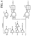
- the calibration control 64 controls the sequencing and overall flow of the calibration. Calibration is performed only when a calibrate signal CAL is high. The calibrate signal CAL is high during the calibration mode of operation, and it is low during the normal mode of operation.
- a first inverter 70 provides the inverted calibration signal or reset calibration signal RESET_CAL. The reset calibration signal RESET_CAL commands the test signal source 66 to generate the test signal I test .
- the fifth address bit A5, the most significant bit of the count, selects the coarse or fine calibration circuit 14 or 16.
- An input of a second inverter 72 receives the address bit A5 and an output of the second inverter 72 provides the signal A5b.
- First and second single-shot latches 74 and 76 may be used to control the sequencing of the calibration events.
- the single shot latches 74 and 76 are reset through NAND gates 78 and 80 when the signal SS_RESET is high.
- An input of a third inverter 82 is connected to the node K.
- An output of the third inverter 82 provides the inverted signal Vtb and a fourth inverter 84 provides the non-inverted signal Vt.
- signals Vt and Vtb provided by the third and fourth inverters 82 and 84 indicate whether a voltage excursion has occurred.
- coarse calibration begins with a maximum negative offset. Each count up to thirty one reduces the offset.
- the voltage excursion occurs, that is, the signal Vt changes from a 0 to 1 or vice-versa
- the first one shot 74 is triggered, whereby the count is held in the latches 44a to 44e of the coarse calibration circuit 14. Even as the count is further incremented, the count that corresponds to the voltage excursion will be held in the latches 44a to 44e.
- the calibration control 64 also filters out switching transients during the current comparison.
- a first input of a third NAND gate 86 is connected to the node K through the third inverter 82, and a second input of the third NAND gate 86 is supplied with a test clock TCLK. When the test clock TCLK is high, the results of the current comparison are supplied to the first one-shot 74 during coarse calibration.
- a first input of a fourth NAND gate 88 is connected to the node K through the third and fourth inverters 82 and 84, and a second input to the fourth NAND gate 88 is supplied with the test clock TCLK. When the test clock TCLK is high, the results of the current comparison are supplied to the second one-shot 76 during fine calibration.
- the switch transitions are restricted to the periods when the test clock TCLK is low. This allows for switching transitions and the circuit to settle to a stable value before testing the voltage at the node K.
- the third and fourth NAND gates 86 and 88 and the test clock TCLK are used to filter out switching transients and settling time effects that occur on the node K when the matching condition is being approached.
- Counter frequency should be slower than the settling time.
- a 10 MHz counter 68 which has a counter period of ten microseconds, may be used if the settling time is about one microsecond.
- a counter period that is longer than ten microseconds would be acceptable.
- a shorter counter period might run the risk of incomplete settling, which could cause errors in the offset calibration process.
- the circuit 10 may be fabricated using a 0.5 micron ASIC CMOS process.
- the counter 68 may be located off-chip, whereby the count is supplied to I/O pads of the chip. However, it may be desirable to move the counter 68 onto the chip.
- the test current source 66 should be on-chip and it should be physically close to the charge amplifier 12. Each charge amplifier 12 is provided with its own test current source 66 in applications such as sensing MRAM memory cells, where many charge amplifiers 12 may be operating simultaneously. Another reason for locating the test current source 66 on-chip is that the magnitude of the test current is small (on the order of 0.5uA) and the current difference sensed during calibration is on the order of nano-amps. An on-chip test current source 66 is less subject to noise for the low current test conditions.
- the test current source 66 may be controlled by an external voltage reference (Vref in Figure 1) or the reference voltage may be generated on the chip.
- Figure 5 shows a method of performing the offset calibration.
- Test and input signals are generated (block 102).
- the input signal is supplied to an input of the charge amplifier.
- the charge amplifier In response to the input signal, the charge amplifier generates an output signal.
- Coarse calibration is performed first.
- An initial back gate bias voltage is applied to the isolated wells in the substrate (block 104).
- the initial back gate bias voltage causes a large initial offset I test > I out .
- the test signal I test is then compared to the output signal I out (block 106). If there is no voltage excursion (block 108), that is, if I test > I out , the back gate bias voltage is adjusted in a small steps (block 110) and another comparison is performed (block 106).
- the back gate bias voltage is adjusted in small steps until a voltage excursion occurs, that is, until I test ⁇ I out .
- a first number corresponding to the back gate bias voltage that caused the voltage excursion is stored in the coarse calibration circuit 14 (block 112). The coarse calibration is now finished.
- Fine calibration is then performed while the back gate bias voltage that caused the comparison change is being applied to the isolated wells.
- An initial transistor impedance is selected to cause I test ⁇ I out (block 114).
- the test signal is then compared to the output signal (block 116). If I test ⁇ I out (block 118), the transistor impedance is incrementally adjusted (block 120) and another comparison is performed (block 118).
- the transistor impedance is adjusted until I test ⁇ I out . Once the voltage excursion occurs, a second number corresponding to the transistor impedance that caused the voltage excursion is stored in memory (block 122). The fine calibration is now finished.
- Figure 6 shows a method of operating the circuit 10 during a normal mode
- the back gate bias voltage corresponding to the stored first number is applied to the isolated wells in the substrate (block 202), and the transistor impedance corresponding to the stored second number is selected (block 204).
- An input signal is then be applied to the operational amplifier (block 206).
- an operational amplifier circuit having digital offset calibration Calibration data does not drift with normal leakage currents.
- a switched capacitor circuit uses a large, isolated capacitor to store the analog offset data
- the circuit having digital offset calibration stores the offset data in conventional CMOS static latches.
- the offset calibration data stored on the large capacitor is subject to degradation due to leakage currents.
- the latches hold a valid state until updated with new digital data.
- FIG. 7 shows an application for the operational amplifier circuits 10: the operational amplifier circuits 10 are used as direct injection charge amplifiers 308 in an MRAM device 310.
- the MRAM device 310 includes an array of memory cells 312. Traces functioning as bit lines 314 extend along columns of the memory cells 312. Each column is a potential source of an input current.
- the bit lines 314 of multiple contiguous columns are multiplexed into a single charge amplifier 308 by a steering circuit 316.
- the steering circuit 316 includes a set of switches that connect each bit line 314 to either a constant voltage source or to a charge amplifier 308.
- the steering circuit 316 further includes a column decoder.
- the column decoder selects only one switch to connect only a selected bit line 314 to the sense amplifier (the current steering switch). All other (unselected) bit lines 314 are be connected to the constant voltage source.
- the constant voltage source may be supplied from an external circuit, and it may be used to set the output voltage of the charge amplifier 308 during the calibration and normal modes of operation.
- An input signal on the selected bit line 314 is steered to the charge amplifier 308 and compared to the test current source 66.
- the input signal includes current from a selected MRAM memory cell 312 (that is, a memory cell crossed by word and bit lines that have been selected) and parasitic currents in the MRAM array.
- the parasitic currents in the MRAM array can arise from the voltage across the unselected memory cells 312 not being precisely equal to the applied array voltage. If the offset error is not properly calibrated, large parasitic currents can occur during sensing of the memory cells 312. These large parasitic currents can cause errors in sensing the resistance of the MRAM memory cells 312.
- the operation of the charge amplifier 308 is to minimize the voltage difference across the unselected array elements.
- the charge amplifier 308 controls the voltage across the memory cells 312 connected to the selected bit line 314, independent of a sense current flowing through the selected memory cell 312.
- a constant voltage is applied to all memory cells 312 (that is an equipotential across the memory cells)
- variations in resistance do not cause a current variation across the remaining parallel memory cells 312 and, thus, the parasitic sense current is made substantially less than the sense current.
- the current that flows in the charge amplifier 308 is directly proportional to the resistance of the selected memory cell 312 without having to make corrections or adjustments for variations in sense voltage.
- An integrator capacitor 318 is charged by the sense current. Charge time is partly dependent upon the resistance of the selected memory cell 312.
- a sense amplifier (not shown) uses the charge time of the capacitor 318 to determine the resistance of the selected memory cell 312. The resistance is either at a first state R or a second state R+ ⁇ R.
- the calibration circuits 14, 16, 64 and 66, 68 also correct for errors in the current steering circuit 316 and other circuits forming a part of the input current path. This effect greatly relaxes the design tolerances of the circuit design with respect to the sizing of current steering devices and multiplexer switches.
- Additional sets of steering circuits 316 and charge amplifiers 308 can receive input signals from other columns of memory cells (not shown). These additional sets can operate in parallel and independently of one another. To access an m-bit word, up to m sets of steering circuits 316 and charge amplifiers 308 are operated in parallel. A single control signal (not shown) controls all of the steering circuits 316 simultaneously.
- Each charge amplifier 308 may be calibrated independently of the other charge amplifiers 308 in the MRAM device 310. However, all may be calibrated at the same time and may share the same set of external calibration and counter signals.
- Figure 8 shows a circuit 410 including an operational amplifier 412 such as a unity gain amplifier or transimpedance amplifier, coarse and fine calibration circuits 414 and 416, a calibration control 464, a test signal source 466, a counter 468, and a circuit 469 for sensing when the output current is within an acceptable limit of the test current for each of the coarse and fine calibrations.
- the present invention is not limited to two stage calibration.
- Single stage calibration may be performed by adjusting the back gate bias voltage.
- the number of voltage dividers may be increased to provide a greater resolution for the back gate bias voltage.
- single stage calibration may be performed by changing the transistor impedance.
- the number of transistors in the first and second programmable circuits 46 and 48 may be increased to provide a greater number of impedance levels in the current mirrors.
Abstract
Description
- The invention relates to operational amplifiers. More specifically, the invention relates to offset error calibration in an operational amplifier.
- There are many different uses for operational amplifiers. For example, operational amplifiers may be used as unity gain amplifiers and transimpedance amplifiers. They may also be used as direct injection charge amplifiers.
- Offset error can be an important issue in the design of operational amplifiers. For instance, the output of a typical unity gain amplifier without offset error correction is
- The source of offset error may arise from the physical design of the operational amplifier or it may arise from process variations. Circuit thresholds, the mismatch of device sizes, and circuit operating conditions are all sources of offset error. Physical size variations inherent in the process of integrated circuits and process parameter variations are sources of offset error that come from manufacturing processes and are basic limitations of the process technology. In CMOS operational amplifiers, threshold voltage process variations provide a major source of offset error.
- Different analog techniques for calibrating offset error have been suggested. One analog technique involves correct transistor sizing and careful physical layout to minimize the basic offset parameters. Even with an optimal design, however, offset correction by design alone might not be good enough to hold the offset voltage to within tens of micro-volts.
- Another analog technique involves the use of a switched capacitor circuit for correcting offset error. A typical switched capacitor circuit uses a high gain operational amplifier to correct for differential amplifier offsets. One disadvantage of this circuit is the use of a large offset correction capacitor to sample and hold offset correction data. The capacitor is made large to minimize leakage and decay effects. Fabrication of the large capacitor also involves special IC process steps and a considerable amount of circuit area. Also, a control requirement to hold the offset voltage to within tens of micro-volts results in a very high refresh rate.
- Yet another technique involves analog controlled offset calibration. Differential current modification is described as a 'nulling input port circuit' in Enz and Gabor; "Circuit Techniques for Reducing the Effects of Op-Amp Imperfections: Autozeroing, Correlated Double Sampling, and Chopper Stabilization"; Proceedings of the IEEE, Vol. 84, No 11, November, 1996, page 1597. Gm modification is described as correction with a 'programmable current mirror' in Yu and Geiger, "Nonideality Consideration for High-Precision Amplifier - Analysis of Random Common Mode Rejection Ratio"; IEEE Transactions on Circuits and Systems;
Vol 40,No 1; January 1993; pages 1-12. With both of these analog techniques, special analog circuitry is used to generate analog control signals. Additional circuits are used to sample and store the analog control signals. Normal circuit leakage currents result in analog control signal data being refreshed frequently. In gm modification and differential current modification, the analog control techniques are subject to the same sample and hold limitations as the switched capacitor technique. - According to one aspect of the invention, digital offset calibration is performed by an integrated circuit having a calibration mode of operation and a normal mode of operation. An operational amplifier of the integrated circuit includes a plurality of transistors, some of which are in isolated wells in a substrate. The transistors provide a controlled current path. A programmable calibration circuit of the integrated circuit is responsive to a digital value. The calibration circuit may provide a back gate bias voltage to at least one of the isolated wells in the substrate and/or adjust impedance of the transistors providing the controlled current path. Level of the back gate bias voltage and an amount of impedance adjustment are determined by the digital value.
- The integrated circuit further includes a test circuit operable during the calibration mode. The test circuit includes a test signal source and a number generator for providing a plurality of different numbers to the calibration circuit while an input signal is being supplied to an input of the operational amplifier. The operational amplifier provides an output signal in response to the input signal.
- The integrated circuit also includes memory for storing a digital value that causes the output signal to be within a desired limit of the test signal during the calibration mode. The memory provides the stored value to the calibration circuit during the normal mode of operation.
- Other aspects and advantages of the present invention will become apparent from the following detailed description, taken in conjunction with the accompanying drawings, illustrating by way of example the principles of the invention.
-
- Figure 1 is an illustration of a direct injection charge amplifier having digital offset calibration;
- Figure 1a is an illustration of a charge amplifier transistor in an isolated well in a substrate;
- Figure 2 is an illustration of a coarse calibration circuit for the amplifier of Figure 1;
- Figure 3 is an illustration of a fine calibration circuit for the amplifier of Figure 1;
- Figure 4 is an illustration of a control circuit for the amplifier of Figure 1;
- Figure 5 is a flowchart of a method of calibrating the amplifier for offset error;
- Figure 6 is a flowchart of a method of operating the amplifier during a normal mode;
- Figure 7 is an illustration of a device including multiple direct injection charge amplifiers; and
- Figure 8 is an illustration of an alternative embodiment of the amplifier of Figure 1.
-
- As shown in the drawings for purposes of illustration, the present invention is embodied in an integrated circuit including a direct injection charge amplifier having digital offset calibration. Because calibration is performed digitally, calibration data does not drift with normal leakage currents. Therefore, the use of special analog components (e.g., low leakage transistors, resistors and linear capacitors) is avoided. Moreover, the offset correction can be performed by an auto-calibration process. Additionally, the digital offset correction corrects for errors in current steering circuitry and other circuits forming a part of the input current path of the direct injection charge amplifier.
- Reference is made to Figure 1, which shows a
circuit 10 including a directinjection charge amplifier 12, acoarse calibration circuit 14 and afine calibration circuit 16 formed on a substrate. Thecharge amplifier 12 includes a PMOS differential amplifier. First, second andthird PMOS transistors second NMOS transistors NMOS transistors PMOS transistors well 6 in asubstrate 8 may be formed by two P-type diffusions oxide barrier 5 and covered by a gate electrode 7 (see Figure 1a). An N-type diffusion 4c in thewell 6 is used as a contact to the well 6 (Again, see Figure 1a). These N-type diffusions allow the back gate bias of the first andsecond PMOS transistors PMOS transistors - The differential amplifier is followed by a second stage amplifier circuit including two
transistors first PMOS transistor 18a, followed by the second stageoperational amplifier circuit current source transistor 26. The feedback signal is the output voltage Vout and the loop is closed when the output voltage Vout is applied to the gate of thefirst PMOS transistor 18a. - As a consequence of working with a high gain amplifier, closed loop stability becomes an issue. Frequency compensation components (a resistor-
capacitor compensation circuit 22, 24) controls the stability of the second stage operational amplifier circuit by reducing high frequency gain of the second stage amplifier circuit and thereby preventing the closed loop operational amplifier from going unstable. - The direct
injection charge amplifier 12 further includes thecurrent source transistor 26, which has a gate coupled to an output of theR-C circuit 22/24 and a drain-source path coupled to an input of the differential amplifier. In the normal operation mode, thecircuit 10 senses and controls the output voltage Vout to a prescribed value by adjusting the current in thecurrent source transistor 26 and then holding the current in thecurrent source transistor 26 constant during a period of time. - The
coarse calibration circuit 14 performs coarse offset correction during a normal mode of operation. Thecoarse calibration circuit 14 performs the coarse correction by applying a back gate bias voltage Vcc+ and Vcc- to the isolated wells of the first andsecond PMOS transistors coarse calibration circuit 14. The sensitivity of the offset voltage to back gate voltage variations can be rather large. Therefore, applying the back gate bias voltage Vcc+ and Vcc- is better suited for making coarse corrections to the offset voltage. - The
fine calibration circuit 16 performs fine offset correction during the normal mode of operation. The fine correction is performed by adjusting impedance of thetransistors fine calibration circuit 16. - Reference is now made to Figure 2, which shows the
coarse calibration circuit 14 in greater detail. Thecoarse calibration circuit 14 includes a pair ofprogrammable voltage dividers PMOS transistors voltage divider - The
first voltage divider 28 is shown, by way of example, as being formed by upper andlower transistors middle transistors numbers 10/1, 1/10, 2/10, 4/10 and 8/10 represent transistor length to width size the for voltage divider. Transistor size variations set the voltage divider ratios. Turning ON different combinations of themiddle transistors first PMOS transistor 18a. - The
second voltage divider 36 also includes upper andlower transistors middle transistors middle transistors second PMOS transistor 18b. - During the normal mode of operation, the
middle transistors static latches fifth latch 44e controls thelower transistors coarse calibration circuit 14 shown in Figure 2 can control the back gate bias voltage Vcc+ and Vcc- to as many as 25 different levels. - Thus, the first number determines the back gate bias voltage Vcc+ and Vcc- applied to the isolated wells of the first and
second PMOS transistors static latches - Reference is now made to Figure 3, which shows the
fine calibration circuit 16 in greater detail. Thefine calibration circuit 16 includes first and secondprogrammable circuits second NMOS transistors programmable circuit 46 is shown, by way of example, as being formed by a first pair oftransistors middle transistors middle transistors - The second
current mirror 48 is also shown, by way of example, as being formed by a second pair oftransistors middle transistors middle transistors - During the normal mode of operation, the
middle transistors static latches - A
fifth latch 62e controls thetransistors fine calibration circuit 16 shown in Figure 3 can control the transistor impedance to as many as 25 different levels. - Thus, the second number determines the impedance of the
transistors static latches - Reference is once again made to Figure 1. The
integrated circuit 10 further includes acalibration control 64, a testcurrent source 66 and acounter 68 for determining the first and second numbers that should be stored in the coarse andfine calibration circuits current source 66 supplies a test current Itest to a node K. The magnitude of the test signal current Itest may be selected to be approximately the value of the expected output signal current Iout in the absence of offset error. - At the start of the calibration mode, the
counter 68 begins counting from zero. The count is supplied to thelatches 44a to 44e and 62a to 62e of the coarse andfine calibration circuits charge amplifier 12, the voltage Vtest at the node K is pulled high, and when the test current Itest is less than or equal to the output current Iout the voltage Vtest at the node K is pulled low. When the node K goes from high to low or vice-versa, the voltage excursion at the node K is large enough to serve as a logic input to CMOS logic gates in thecalibration control 64. When this voltage excursion occurs (that is, the new count causes the back gate bias voltage to change such that Itest is less than or equal to Iout), the number that caused the voltage excursion is held in thelatches 44a to 44e of thecoarse calibration circuit 14. That number will be used to set the back gate bias voltage Vcc+ and Vcc- during the normal mode of operation. - The number held in the
latches 44a to 44e of thecoarse calibration circuit 14 is also used to set the back gate bias voltage Vcc+ and Vcc- during fine calibration. As the count is further incremented (and bit A5=0), the number stored in thelatches 44a to 44e does not change. After the count has reached 25, the next increment causes the most significant bit A5 to go high, the remaining bits A0 to A4 to go low, and the fine calibration to begin. The initial level of the test current Itest is less than the output current Iout. Each time the count is incremented during fine calibration, the transistor impedance is changed to a new level. When another large voltage excursion occurs (due to the new count causing the transistor impedance to change such that that Itest is greater than or equal to Iout), the number that caused the voltage excursion is held in thelatches 62a to 62e of thefine calibration circuit 16. That number will be used to set the transistor impedance during the normal mode of operation. - Additional reference is now made to Figure 4. The
calibration control 64 controls the sequencing and overall flow of the calibration. Calibration is performed only when a calibrate signal CAL is high. The calibrate signal CAL is high during the calibration mode of operation, and it is low during the normal mode of operation. Afirst inverter 70 provides the inverted calibration signal or reset calibration signal RESET_CAL. The reset calibration signal RESET_CAL commands thetest signal source 66 to generate the test signal Itest. - The fifth address bit A5, the most significant bit of the count, selects the coarse or
fine calibration circuit second inverter 72 receives the address bit A5 and an output of thesecond inverter 72 provides the signal A5b. When the single shot reset signal SS_RESET is low and the most significant bit A5 is low, coarse calibration is performed. When the single shot reset signal SS_RESET is low and the most significant bit A5 is high, fine calibration is performed. - First and second single-shot latches 74 and 76 may be used to control the sequencing of the calibration events. The single shot latches 74 and 76 are reset through
NAND gates - An input of a
third inverter 82 is connected to the node K. An output of thethird inverter 82 provides the inverted signal Vtb and afourth inverter 84 provides the non-inverted signal Vt. Thus, signals Vt and Vtb provided by the third andfourth inverters inverter 84 is provided; it accounts for the difference in testing the node K.) - If the count starts at 0, coarse calibration begins with a maximum negative offset. Each count up to thirty one reduces the offset. Once the voltage excursion occurs, that is, the signal Vt changes from a 0 to 1 or vice-versa, the first one shot 74 is triggered, whereby the count is held in the
latches 44a to 44e of thecoarse calibration circuit 14. Even as the count is further incremented, the count that corresponds to the voltage excursion will be held in thelatches 44a to 44e. - When the count reaches thirty two, the most significant bit A5 is high and the other four bits A0 to A4 are low. Thus, coarse calibration is ended, and fine calibration begins with the maximum negative offset. Each subsequent increment reduces the offset.
- The
calibration control 64 also filters out switching transients during the current comparison. A first input of athird NAND gate 86 is connected to the node K through thethird inverter 82, and a second input of thethird NAND gate 86 is supplied with a test clock TCLK. When the test clock TCLK is high, the results of the current comparison are supplied to the first one-shot 74 during coarse calibration. Similarly, a first input of afourth NAND gate 88 is connected to the node K through the third andfourth inverters fourth NAND gate 88 is supplied with the test clock TCLK. When the test clock TCLK is high, the results of the current comparison are supplied to the second one-shot 76 during fine calibration. The switch transitions are restricted to the periods when the test clock TCLK is low. This allows for switching transitions and the circuit to settle to a stable value before testing the voltage at the node K. Thus, the third andfourth NAND gates - Counter frequency should be slower than the settling time. For example, a 10
MHz counter 68, which has a counter period of ten microseconds, may be used if the settling time is about one microsecond. A counter period that is longer than ten microseconds would be acceptable. A shorter counter period might run the risk of incomplete settling, which could cause errors in the offset calibration process. - The
circuit 10 may be fabricated using a 0.5 micron ASIC CMOS process. Thecounter 68 may be located off-chip, whereby the count is supplied to I/O pads of the chip. However, it may be desirable to move thecounter 68 onto the chip. - The test
current source 66 should be on-chip and it should be physically close to thecharge amplifier 12. Eachcharge amplifier 12 is provided with its own testcurrent source 66 in applications such as sensing MRAM memory cells, wheremany charge amplifiers 12 may be operating simultaneously. Another reason for locating the testcurrent source 66 on-chip is that the magnitude of the test current is small (on the order of 0.5uA) and the current difference sensed during calibration is on the order of nano-amps. An on-chip testcurrent source 66 is less subject to noise for the low current test conditions. The testcurrent source 66 may be controlled by an external voltage reference (Vref in Figure 1) or the reference voltage may be generated on the chip. - Figure 5 shows a method of performing the offset calibration. Test and input signals are generated (block 102). The input signal is supplied to an input of the charge amplifier. In response to the input signal, the charge amplifier generates an output signal.
- Coarse calibration is performed first. An initial back gate bias voltage is applied to the isolated wells in the substrate (block 104). For example, the initial back gate bias voltage causes a large initial offset Itest > Iout. The test signal Itest is then compared to the output signal Iout (block 106). If there is no voltage excursion (block 108), that is, if Itest > Iout, the back gate bias voltage is adjusted in a small steps (block 110) and another comparison is performed (block 106). The back gate bias voltage is adjusted in small steps until a voltage excursion occurs, that is, until Itest ≤ Iout. Once the voltage excursion occurs, a first number corresponding to the back gate bias voltage that caused the voltage excursion is stored in the coarse calibration circuit 14 (block 112). The coarse calibration is now finished.
- Fine calibration is then performed while the back gate bias voltage that caused the comparison change is being applied to the isolated wells. An initial transistor impedance is selected to cause Itest < Iout (block 114). The test signal is then compared to the output signal (block 116). If Itest < Iout (block 118), the transistor impedance is incrementally adjusted (block 120) and another comparison is performed (block 118). The transistor impedance is adjusted until Itest ≥ Iout. Once the voltage excursion occurs, a second number corresponding to the transistor impedance that caused the voltage excursion is stored in memory (block 122). The fine calibration is now finished.
- Although the coarse and fine calibration described above began with negative offsets (Itest > Iout), they could have begun instead with large positive offsets (Itest < Iout). Had the initial offset been positive for both coarse and fine calibration, the back gate bias voltage and transistor impedance would have been stepped down in small, digitally controlled steps until Itest ≥ Iout.
- Figure 6 shows a method of operating the
circuit 10 during a normal mode The back gate bias voltage corresponding to the stored first number is applied to the isolated wells in the substrate (block 202), and the transistor impedance corresponding to the stored second number is selected (block 204). An input signal is then be applied to the operational amplifier (block 206). - Thus disclosed is an operational amplifier circuit having digital offset calibration. Calibration data does not drift with normal leakage currents. Whereas a switched capacitor circuit uses a large, isolated capacitor to store the analog offset data, the circuit having digital offset calibration stores the offset data in conventional CMOS static latches. Whereas the offset calibration data stored on the large capacitor is subject to degradation due to leakage currents. The latches hold a valid state until updated with new digital data. Thus, the use of special analog components such as low leakage transistors, resistors, or linear capacitors is avoided.
- Figure 7 shows an application for the operational amplifier circuits 10: the
operational amplifier circuits 10 are used as directinjection charge amplifiers 308 in anMRAM device 310. TheMRAM device 310 includes an array ofmemory cells 312. Traces functioning asbit lines 314 extend along columns of thememory cells 312. Each column is a potential source of an input current. The bit lines 314 of multiple contiguous columns are multiplexed into asingle charge amplifier 308 by asteering circuit 316. - The
steering circuit 316 includes a set of switches that connect eachbit line 314 to either a constant voltage source or to acharge amplifier 308. Thesteering circuit 316 further includes a column decoder. The column decoder selects only one switch to connect only a selectedbit line 314 to the sense amplifier (the current steering switch). All other (unselected) bitlines 314 are be connected to the constant voltage source. The constant voltage source may be supplied from an external circuit, and it may be used to set the output voltage of thecharge amplifier 308 during the calibration and normal modes of operation. - An input signal on the selected
bit line 314 is steered to thecharge amplifier 308 and compared to the testcurrent source 66. The input signal includes current from a selected MRAM memory cell 312 (that is, a memory cell crossed by word and bit lines that have been selected) and parasitic currents in the MRAM array. The parasitic currents in the MRAM array can arise from the voltage across theunselected memory cells 312 not being precisely equal to the applied array voltage. If the offset error is not properly calibrated, large parasitic currents can occur during sensing of thememory cells 312. These large parasitic currents can cause errors in sensing the resistance of theMRAM memory cells 312. The operation of thecharge amplifier 308 is to minimize the voltage difference across the unselected array elements. - The
charge amplifier 308 controls the voltage across thememory cells 312 connected to the selectedbit line 314, independent of a sense current flowing through the selectedmemory cell 312. When a constant voltage is applied to all memory cells 312 (that is an equipotential across the memory cells), variations in resistance do not cause a current variation across the remainingparallel memory cells 312 and, thus, the parasitic sense current is made substantially less than the sense current. The current that flows in thecharge amplifier 308 is directly proportional to the resistance of the selectedmemory cell 312 without having to make corrections or adjustments for variations in sense voltage. - An
integrator capacitor 318 is charged by the sense current. Charge time is partly dependent upon the resistance of the selectedmemory cell 312. A sense amplifier (not shown) uses the charge time of thecapacitor 318 to determine the resistance of the selectedmemory cell 312. The resistance is either at a first state R or a second state R+ΔR. - The
calibration circuits current steering circuit 316 and other circuits forming a part of the input current path. This effect greatly relaxes the design tolerances of the circuit design with respect to the sizing of current steering devices and multiplexer switches. - Additional sets of steering
circuits 316 andcharge amplifiers 308 can receive input signals from other columns of memory cells (not shown). These additional sets can operate in parallel and independently of one another. To access an m-bit word, up to m sets of steeringcircuits 316 andcharge amplifiers 308 are operated in parallel. A single control signal (not shown) controls all of thesteering circuits 316 simultaneously. - Each
charge amplifier 308 may be calibrated independently of theother charge amplifiers 308 in theMRAM device 310. However, all may be calibrated at the same time and may share the same set of external calibration and counter signals. - Although the
operational amplifier circuit 10 may be used for sensing the resistance of MRAM memory cells, it is not limited to such an application. Moreover, the present invention is not limited to direct injection charge amplifiers. For example, Figure 8 shows acircuit 410 including anoperational amplifier 412 such as a unity gain amplifier or transimpedance amplifier, coarse andfine calibration circuits calibration control 464, atest signal source 466, acounter 468, and acircuit 469 for sensing when the output current is within an acceptable limit of the test current for each of the coarse and fine calibrations. - The present invention is not limited to two stage calibration. Single stage calibration may be performed by adjusting the back gate bias voltage. For such calibration, the number of voltage dividers may be increased to provide a greater resolution for the back gate bias voltage.
- Similarly, single stage calibration may be performed by changing the transistor impedance. For such calibration, the number of transistors in the first and second
programmable circuits - Accordingly, the invention is not limited to the specific embodiments described and illustrated above. Instead, the invention is construed according to the claims that follow.
Claims (8)
- An integrated circuit (10) having a calibration mode of operation and a normal mode of operation, the circuit (10) comprising:an operational amplifier including a plurality of transistors (18a, 18b, 18c, 18d, 18e) for providing a controlled current path, at least some of the transistors (18a, 18b) being in isolated wells (6) in a substrate (8);a programmable calibration circuit (14, 16), responsive to a digital value, for performing at least one of (a) providing a back gate bias voltage to at least one isolated well and (b) adjusting impedance of the transistors providing the controlled current path, level of the back gate bias voltage and an amount of impedance adjustment being determined by the digital value, whereby different digital values may be supplied to the programmable calibration circuit (14, 16) during the calibration mode of operation;a test circuit including a test signal source (66) for generating a test signal during the calibration mode of operation; andmemory (44a to 44e, 62a to 62e) for storing a digital value that causes an output signal from the operational amplifier to be within a desired limit of the test signal during the calibration mode, the memory (44a to 44e, 62a to 62e) providing the stored value to the calibration circuit during the normal mode of operation.
- The circuit of claim 1, wherein the programmable calibration circuit includes:a coarse calibration circuit (14), responsive to the digital value, for applying a desired back gate correction voltage to at least one isolated well; anda fine calibration circuit (16) for adjusting the impedance of the transistors providing the controlled current path, the impedance being adjusted in response to the digital value.
- The circuit of claim 2, wherein the test circuit further includes a control (64) for ending the coarse calibration when a comparison of test signal current amplitude to output current amplitude is reversed and for ending the fine calibration when a comparison of test signal current amplitude to output current amplitude is reversed, the control (64) causing a first portion of the digital value to be stored in the memory (44a to 44e) when the coarse calibration is ended, the control (64) causing a second portion of the digital value to be stored in the memory (62a to 62e) when the fine calibration is ended.
- The circuit of claim 3, further comprising an additional transistor (26) having a gate coupled to an output of the operational amplifier, the additional transistor (26) having a drain-source path coupled to the test signal source (66), a voltage drop along the drain-source path indicating when the comparison is reversed.
- The circuit of claim 2, wherein the coarse calibration circuit (14) includes a plurality of first transistors (30, 32, 34a to 34d, 38, 40 and 42a to 42d) forming a plurality of voltage dividers, the first transistors being selected to apply the back gate bias voltage to at least one isolated well; and wherein the fine calibration circuit includes a plurality of second transistors (50, 52, 54a to 54d, 56, 58 and 60a to 60d), the second transistors being selected to adjust the impedance of the transistors providing the controlled current path.
- The circuit of claim 2, wherein the digital value includes first and second numbers; and wherein the memory includes a plurality of first registers (44a to 44e) for storing the first number during the calibration mode and a plurality of second registers (62a to 62e) for storing the second number during the calibration mode, the plurality of first registers (44a to 44e) supplying the first number to the coarse calibration circuit (14) during the normal mode and during the fine calibration of the calibration mode, the plurality of second registers (62a to 62e) supplying the second number to the fine calibration circuit (16) during the normal mode.
- The circuit of claim 6, wherein the test circuit further includes a control 64) and first and second one-shots (74, 76), the control (64) triggering the first one-shot (74) when the coarse calibration is finished, the first triggered one-shot (74) causing the first number to be held in the first plurality of registers (44a to 44e), the fine calibration being performed after the coarse calibration has been performed, the control (64) causing the second one-shot (76) to be triggered when the fine calibration is finished, the triggered second one-shot (76) causing the second number to be held in the second plurality of registers (62a to 62e).
- The circuit of claim 2, further comprising a modulo counter (68) for providing a plurality of different digital values to the calibration circuit (14,16) during the calibration mode.
Applications Claiming Priority (2)
| Application Number | Priority Date | Filing Date | Title |
|---|---|---|---|
| US430238 | 1999-10-29 | ||
| US09/430,238 US6262625B1 (en) | 1999-10-29 | 1999-10-29 | Operational amplifier with digital offset calibration |
Publications (2)
| Publication Number | Publication Date |
|---|---|
| EP1104092A2 true EP1104092A2 (en) | 2001-05-30 |
| EP1104092A3 EP1104092A3 (en) | 2005-07-27 |
Family
ID=23706678
Family Applications (1)
| Application Number | Title | Priority Date | Filing Date |
|---|---|---|---|
| EP00118854A Withdrawn EP1104092A3 (en) | 1999-10-29 | 2000-08-31 | Operational amplifier with digital offset calibration |
Country Status (3)
| Country | Link |
|---|---|
| US (1) | US6262625B1 (en) |
| EP (1) | EP1104092A3 (en) |
| JP (1) | JP4657438B2 (en) |
Cited By (12)
| Publication number | Priority date | Publication date | Assignee | Title |
|---|---|---|---|---|
| WO2002073618A2 (en) * | 2001-03-14 | 2002-09-19 | Infineon Technologies Ag | Memory sense amplifier for a semiconductor memory device |
| EP1260988A2 (en) * | 2001-05-14 | 2002-11-27 | Hewlett-Packard Company | Resistive cross point memory device with calibration controller for a sense amplifier |
| EP1441438A1 (en) * | 2003-01-23 | 2004-07-28 | Hewlett-Packard Development Company, L.P. | An adjustable offset differential amplifier |
| EP1526549A1 (en) * | 2003-10-03 | 2005-04-27 | Hewlett-Packard Development Company, L.P. | System and method of calibrating a read circuit in a magnetic memory |
| US7006373B2 (en) | 2001-06-28 | 2006-02-28 | Renesas Technology Corp. | Thin film magnetic memory device with memory cells including a tunnel magnetic resistive element |
| EP2086111A3 (en) * | 2008-01-31 | 2010-01-13 | Imec | Large time constant steering circuit and instrumentation amplifier implementing same |
| EP2442311A1 (en) * | 2010-10-13 | 2012-04-18 | Taiwan Semiconductor Manufacturing Company, Ltd. | Offset compensation for sense amplifiers |
| EP2797231A1 (en) * | 2013-04-22 | 2014-10-29 | Samsung Display Co., Ltd. | Mismatched differential circuit |
| US9344305B2 (en) | 2013-04-22 | 2016-05-17 | Samsung Display Co., Ltd. | PVT tolerant differential circuit |
| EP3121679A3 (en) * | 2015-07-23 | 2017-04-26 | NXP USA, Inc. | Programmable resistive elements as variable tuning elements |
| CN109104162A (en) * | 2018-08-08 | 2018-12-28 | 义乌工商职业技术学院 | A kind of Computer signal compensation circuit |
| CN115833556A (en) * | 2023-02-14 | 2023-03-21 | 珠海智融科技股份有限公司 | Current-limiting calibration method and circuit for power converter chip |
Families Citing this family (48)
| Publication number | Priority date | Publication date | Assignee | Title |
|---|---|---|---|---|
| JP2002299575A (en) * | 2001-03-29 | 2002-10-11 | Toshiba Corp | Semiconductor memory |
| US6854076B2 (en) * | 2001-04-03 | 2005-02-08 | Texas Instruments Incorporated | Method and apparatus for calibration of an electronic device |
| US6597600B2 (en) * | 2001-08-27 | 2003-07-22 | Micron Technology, Inc. | Offset compensated sensing for magnetic random access memory |
| US6538917B1 (en) * | 2001-09-25 | 2003-03-25 | Hewlett-Packard Development Company, L.P. | Read methods for magneto-resistive device having soft reference layer |
| US6501697B1 (en) * | 2001-10-11 | 2002-12-31 | Hewlett-Packard Company | High density memory sense amplifier |
| US6586989B2 (en) * | 2001-11-06 | 2003-07-01 | Hewlett-Packard Development Company, L.P. | Nonlinear digital differential amplifier offset calibration |
| US6759257B2 (en) * | 2001-11-13 | 2004-07-06 | Fujitsu Limited | Structure and method for embedding capacitors in z-connected multi-chip modules |
| US6859095B2 (en) * | 2002-01-31 | 2005-02-22 | Stmicroelectronics Pvt. Ltd. | Non-switched capacitor offset voltage compensation in operational amplifiers |
| US20040019664A1 (en) * | 2002-02-15 | 2004-01-29 | Franck Le | Method and system for discovering a network element in a network such as an agent in an IP network |
| US7203472B2 (en) * | 2002-03-15 | 2007-04-10 | Nokia Corporation | Method and apparatus providing calibration technique for RF performance tuning |
| US6590804B1 (en) | 2002-07-16 | 2003-07-08 | Hewlett-Packard Development Company, L.P. | Adjustable current mode differential amplifier |
| DE10236861B4 (en) * | 2002-08-07 | 2005-11-17 | Albrecht Schmidt | Amplifier with precise digitally adjustable parameters and use of the amplifier |
| US6882218B2 (en) * | 2002-08-26 | 2005-04-19 | Broadcom Corporation | Transimpedance amplifier and offset correction mechanism and method for lowering noise |
| US6674679B1 (en) | 2002-10-01 | 2004-01-06 | Hewlett-Packard Development Company, L.P. | Adjustable current mode differential amplifier for multiple bias point sensing of MRAM having equi-potential isolation |
| US6754123B2 (en) * | 2002-10-01 | 2004-06-22 | Hewlett-Packard Development Company, Lp. | Adjustable current mode differential amplifier for multiple bias point sensing of MRAM having diode isolation |
| US6836429B2 (en) * | 2002-12-07 | 2004-12-28 | Hewlett-Packard Development Company, L.P. | MRAM having two write conductors |
| US6868025B2 (en) * | 2003-03-10 | 2005-03-15 | Sharp Laboratories Of America, Inc. | Temperature compensated RRAM circuit |
| US6667901B1 (en) * | 2003-04-29 | 2003-12-23 | Hewlett-Packard Development Company, L.P. | Dual-junction magnetic memory device and read method |
| US6912150B2 (en) | 2003-05-13 | 2005-06-28 | Lionel Portman | Reference current generator, and method of programming, adjusting and/or operating same |
| US7027318B2 (en) * | 2003-05-30 | 2006-04-11 | Hewlett-Packard Development Company, L.P. | Method and system for adjusting offset voltage |
| US6873543B2 (en) * | 2003-05-30 | 2005-03-29 | Hewlett-Packard Development Company, L.P. | Memory device |
| US7079436B2 (en) * | 2003-09-30 | 2006-07-18 | Hewlett-Packard Development Company, L.P. | Resistive cross point memory |
| US6990030B2 (en) * | 2003-10-21 | 2006-01-24 | Hewlett-Packard Development Company, L.P. | Magnetic memory having a calibration system |
| US6999366B2 (en) * | 2003-12-03 | 2006-02-14 | Hewlett-Packard Development Company, Lp. | Magnetic memory including a sense result category between logic states |
| US7027316B2 (en) * | 2003-12-29 | 2006-04-11 | Micron Technology, Inc. | Access circuit and method for allowing external test voltage to be applied to isolated wells |
| US6980455B2 (en) * | 2004-02-03 | 2005-12-27 | Hewlett-Packard Development Company, L.P. | Remote sensed pre-amplifier for cross-point arrays |
| US7042757B2 (en) * | 2004-03-04 | 2006-05-09 | Hewlett-Packard Development Company, L.P. | 1R1D MRAM block architecture |
| JP3971414B2 (en) * | 2004-07-16 | 2007-09-05 | ローム株式会社 | A / D conversion device and communication device using the same |
| US7224598B2 (en) * | 2004-09-02 | 2007-05-29 | Hewlett-Packard Development Company, L.P. | Programming of programmable resistive memory devices |
| US7394708B1 (en) * | 2005-03-18 | 2008-07-01 | Xilinx, Inc. | Adjustable global tap voltage to improve memory cell yield |
| US7268622B2 (en) * | 2005-11-03 | 2007-09-11 | Samsung Electronics Co., Ltd. | Analog preamplifier calibration |
| US7626416B2 (en) * | 2005-12-12 | 2009-12-01 | Micron Technology, Inc. | Method and apparatus for high resolution ZQ calibration |
| US7603084B2 (en) * | 2006-02-03 | 2009-10-13 | Wionics Technologies, Inc. | Method and apparatus for DC offset calibration |
| US7514954B2 (en) * | 2006-05-10 | 2009-04-07 | Micron Technology, Inc. | Method and apparatus for output driver calibration |
| US7557603B2 (en) * | 2006-08-29 | 2009-07-07 | Micron Technology, Inc. | Method and apparatus for output driver calibration, and memory devices and system embodying same |
| US8161430B2 (en) * | 2008-04-22 | 2012-04-17 | Qualcomm Incorporated | System and method of resistance based memory circuit parameter adjustment |
| WO2010013295A1 (en) * | 2008-07-31 | 2010-02-04 | 国立大学法人広島大学 | Offset elimination circuit, associative memory equipped with the same, and offset voltage elimination method |
| US7696778B1 (en) * | 2009-01-16 | 2010-04-13 | Micron Technology, Inc. | Systems and methods for detecting terminal state and setting output driver impedance |
| JP5493541B2 (en) * | 2009-07-24 | 2014-05-14 | 凸版印刷株式会社 | Evaluation system and evaluation method |
| US8806284B2 (en) * | 2012-05-02 | 2014-08-12 | Avalanche Technology Inc. | Method for bit-error rate testing of resistance-based RAM cells using a reflected signal |
| US9025367B1 (en) * | 2013-11-26 | 2015-05-05 | Realtek Semiconductor Corp. | Method and apparatus for sensing tunnel magneto-resistance |
| US10025685B2 (en) * | 2015-03-27 | 2018-07-17 | Intel Corporation | Impedance compensation based on detecting sensor data |
| US10348270B2 (en) | 2016-12-09 | 2019-07-09 | Micron Technology, Inc. | Apparatuses and methods for calibrating adjustable impedances of a semiconductor device |
| US10193711B2 (en) | 2017-06-22 | 2019-01-29 | Micron Technology, Inc. | Timing based arbitration methods and apparatuses for calibrating impedances of a semiconductor device |
| US10615798B2 (en) | 2017-10-30 | 2020-04-07 | Micron Technology, Inc. | Apparatuses and methods for identifying memory devices of a semiconductor device sharing an external resistance |
| US10552563B2 (en) * | 2018-01-10 | 2020-02-04 | Qualcomm Incorporated | Digital design with bundled data asynchronous logic and body-biasing tuning |
| US10747245B1 (en) | 2019-11-19 | 2020-08-18 | Micron Technology, Inc. | Apparatuses and methods for ZQ calibration |
| US11936352B2 (en) | 2020-03-30 | 2024-03-19 | Apple Inc. | Amplifier circuit with distributed dynamic chopping |
Citations (6)
| Publication number | Priority date | Publication date | Assignee | Title |
|---|---|---|---|---|
| US4806875A (en) * | 1988-05-11 | 1989-02-21 | Maxim Integrated Products | Precision operational amplifier |
| JPH0279608A (en) * | 1988-09-16 | 1990-03-20 | Olympus Optical Co Ltd | Offset adjusting device for operational amplifier |
| US5397944A (en) * | 1993-04-09 | 1995-03-14 | Crystal Semiconductor Corporation | Dense offset calibration circuitry and method |
| JPH08125463A (en) * | 1994-10-21 | 1996-05-17 | Hitachi Ltd | Semiconductor integrated circuit device |
| US5726597A (en) * | 1996-08-30 | 1998-03-10 | Motorola, Inc. | Method and circuit for reducing offset voltages for a differential input stage |
| WO1999007067A1 (en) * | 1997-08-01 | 1999-02-11 | Lsi Logic Corporation | Offset adjustment of cmos matched pairs with body voltage |
Family Cites Families (13)
| Publication number | Priority date | Publication date | Assignee | Title |
|---|---|---|---|---|
| US4754169A (en) * | 1987-04-24 | 1988-06-28 | American Telephone And Telegraph Company, At&T Bell Laboratories | Differential circuit with controllable offset |
| US5059920A (en) * | 1988-12-09 | 1991-10-22 | Synaptics, Incorporated | CMOS amplifier with offset adaptation |
| GB2232841B (en) * | 1989-05-19 | 1994-01-26 | Quantel Ltd | An amplification circuit with temperature compensation |
| JPH04192703A (en) * | 1990-11-26 | 1992-07-10 | Mitsubishi Electric Corp | Mos input differential amplifier circuit |
| US5410265A (en) * | 1993-09-30 | 1995-04-25 | Vimak Corporation | Amplifier calibration apparatus and method therefor |
| JP3257290B2 (en) * | 1994-10-28 | 2002-02-18 | ソニー株式会社 | Comparator and differential amplifier |
| US5565813A (en) * | 1995-05-15 | 1996-10-15 | Motorola Inc. | Apparatus for a low voltage differential amplifier incorporating switched capacitors |
| JP4354539B2 (en) * | 1995-12-20 | 2009-10-28 | テキサス インスツルメンツ インコーポレイテツド | Control of the body effect of MOS transistors |
| JPH09261053A (en) * | 1996-03-18 | 1997-10-03 | Hitachi Ltd | D/a conversion output circuit |
| JPH1168476A (en) * | 1997-08-12 | 1999-03-09 | Sony Corp | Offset adjusting circuit of operation amplifier |
| US6034569A (en) * | 1998-06-11 | 2000-03-07 | Capella Microsystems, Inc. | Amplifier offset cancellation system |
| US5990738A (en) * | 1998-06-19 | 1999-11-23 | Datum Telegraphic Inc. | Compensation system and methods for a linear power amplifier |
| US6043706A (en) * | 1999-02-05 | 2000-03-28 | Ericsson Inc. | Methods and apparatus for controlling power amplifier quiescent current in a wireless communication device |
-
1999
- 1999-10-29 US US09/430,238 patent/US6262625B1/en not_active Expired - Lifetime
-
2000
- 2000-08-31 EP EP00118854A patent/EP1104092A3/en not_active Withdrawn
- 2000-10-27 JP JP2000329103A patent/JP4657438B2/en not_active Expired - Fee Related
Patent Citations (6)
| Publication number | Priority date | Publication date | Assignee | Title |
|---|---|---|---|---|
| US4806875A (en) * | 1988-05-11 | 1989-02-21 | Maxim Integrated Products | Precision operational amplifier |
| JPH0279608A (en) * | 1988-09-16 | 1990-03-20 | Olympus Optical Co Ltd | Offset adjusting device for operational amplifier |
| US5397944A (en) * | 1993-04-09 | 1995-03-14 | Crystal Semiconductor Corporation | Dense offset calibration circuitry and method |
| JPH08125463A (en) * | 1994-10-21 | 1996-05-17 | Hitachi Ltd | Semiconductor integrated circuit device |
| US5726597A (en) * | 1996-08-30 | 1998-03-10 | Motorola, Inc. | Method and circuit for reducing offset voltages for a differential input stage |
| WO1999007067A1 (en) * | 1997-08-01 | 1999-02-11 | Lsi Logic Corporation | Offset adjustment of cmos matched pairs with body voltage |
Non-Patent Citations (5)
| Title |
|---|
| GOODENOUGH F: "LOW-OFFSET AND LOW-POWER UNIVERSAL OP AMPS ARRIVE" ELECTRONIC DESIGN, PENTON PUBLISHING, CLEVELAND, OH, US, vol. 45, no. 9, 1 May 1997 (1997-05-01), pages 145-146,148, XP000728924 ISSN: 0013-4872 * |
| GRIFFITH R ET AL: "SA 21.4: A 1V BICMOS RAIL-RO-RAIL AMPLIFIER WITH N-CHANNEL DEPLETION-MODEL INPUT-STAGE" IEEE INTERNATIONAL SOLID STATE CIRCUITS CONFERENCE, IEEE INC. NEW YORK, US, vol. 40, February 1997 (1997-02), pages 352-353,484, XP000753130 ISSN: 0193-6530 * |
| LEIGHTON H N: "Back Gate Control Circuits" IBM TECHNICAL DISCLOSURE BULLETIN, IBM CORP. NEW YORK, US, vol. 27, no. 6, November 1984 (1984-11), pages 3607-3608, XP002086016 ISSN: 0018-8689 * |
| PATENT ABSTRACTS OF JAPAN vol. 014, no. 259 (E-0937), 5 June 1990 (1990-06-05) & JP 02 079608 A (OLYMPUS OPTICAL CO LTD), 20 March 1990 (1990-03-20) * |
| PATENT ABSTRACTS OF JAPAN vol. 1996, no. 09, 30 September 1996 (1996-09-30) & JP 08 125463 A (HITACHI LTD), 17 May 1996 (1996-05-17) * |
Cited By (22)
| Publication number | Priority date | Publication date | Assignee | Title |
|---|---|---|---|---|
| WO2002073618A2 (en) * | 2001-03-14 | 2002-09-19 | Infineon Technologies Ag | Memory sense amplifier for a semiconductor memory device |
| WO2002073618A3 (en) * | 2001-03-14 | 2003-05-01 | Infineon Technologies Ag | Memory sense amplifier for a semiconductor memory device |
| US6847568B2 (en) | 2001-03-14 | 2005-01-25 | Infineon Technologies Ag | Sense amplifier configuration for a semiconductor memory device |
| EP1260988A2 (en) * | 2001-05-14 | 2002-11-27 | Hewlett-Packard Company | Resistive cross point memory device with calibration controller for a sense amplifier |
| EP1260988A3 (en) * | 2001-05-14 | 2004-08-18 | Hewlett-Packard Company | Resistive cross point memory device with calibration controller for a sense amplifier |
| US7006373B2 (en) | 2001-06-28 | 2006-02-28 | Renesas Technology Corp. | Thin film magnetic memory device with memory cells including a tunnel magnetic resistive element |
| US7313042B2 (en) | 2001-06-28 | 2007-12-25 | Renesas Technology Corp. | Thin film magnetic memory device having an improved read operation margin |
| EP1441438A1 (en) * | 2003-01-23 | 2004-07-28 | Hewlett-Packard Development Company, L.P. | An adjustable offset differential amplifier |
| EP1526549A1 (en) * | 2003-10-03 | 2005-04-27 | Hewlett-Packard Development Company, L.P. | System and method of calibrating a read circuit in a magnetic memory |
| EP2086111A3 (en) * | 2008-01-31 | 2010-01-13 | Imec | Large time constant steering circuit and instrumentation amplifier implementing same |
| EP2442311A1 (en) * | 2010-10-13 | 2012-04-18 | Taiwan Semiconductor Manufacturing Company, Ltd. | Offset compensation for sense amplifiers |
| EP2631911A1 (en) * | 2010-10-13 | 2013-08-28 | Taiwan Semiconductor Manufacturing Co., Ltd. | Offset compensation for sense amplifiers |
| US9322859B2 (en) | 2010-10-13 | 2016-04-26 | Taiwan Semiconductor Manufacturing Company, Ltd. | Offset compensation for sense amplifiers |
| US9509255B2 (en) | 2010-10-13 | 2016-11-29 | Taiwan Semiconductor Manufacturing Company, Ltd. | Offset compensation for sense amplifiers |
| EP2797231A1 (en) * | 2013-04-22 | 2014-10-29 | Samsung Display Co., Ltd. | Mismatched differential circuit |
| US9344305B2 (en) | 2013-04-22 | 2016-05-17 | Samsung Display Co., Ltd. | PVT tolerant differential circuit |
| US9680430B2 (en) | 2013-04-22 | 2017-06-13 | Samsung Display Co., Ltd. | Mismatched differential circuit |
| EP3121679A3 (en) * | 2015-07-23 | 2017-04-26 | NXP USA, Inc. | Programmable resistive elements as variable tuning elements |
| US9935616B2 (en) | 2015-07-23 | 2018-04-03 | Nxp Usa, Inc. | Programmable resistive elements as variable tuning elements |
| CN109104162A (en) * | 2018-08-08 | 2018-12-28 | 义乌工商职业技术学院 | A kind of Computer signal compensation circuit |
| CN109104162B (en) * | 2018-08-08 | 2022-02-18 | 义乌工商职业技术学院 | Computer signal compensation circuit |
| CN115833556A (en) * | 2023-02-14 | 2023-03-21 | 珠海智融科技股份有限公司 | Current-limiting calibration method and circuit for power converter chip |
Also Published As
| Publication number | Publication date |
|---|---|
| JP4657438B2 (en) | 2011-03-23 |
| EP1104092A3 (en) | 2005-07-27 |
| US6262625B1 (en) | 2001-07-17 |
| JP2001185963A (en) | 2001-07-06 |
Similar Documents
| Publication | Publication Date | Title |
|---|---|---|
| US6262625B1 (en) | Operational amplifier with digital offset calibration | |
| US7079436B2 (en) | Resistive cross point memory | |
| US7660161B2 (en) | Integrated flash memory systems and methods for load compensation | |
| US7286428B2 (en) | Offset compensated sensing for magnetic random access memory | |
| US6999366B2 (en) | Magnetic memory including a sense result category between logic states | |
| US6807118B2 (en) | Adjustable offset differential amplifier | |
| US20050099234A1 (en) | Method and system for minimizing differential amplifier power supply sensitivity | |
| US20040095827A1 (en) | Memory cell sensing integrator | |
| US6586989B2 (en) | Nonlinear digital differential amplifier offset calibration | |
| TWI753792B (en) | Sense amplifier and operating moethod for non-volatile memory | |
| US6879534B2 (en) | Method and system for minimizing differential amplifier power supply sensitivity | |
| EP1526549B1 (en) | System and method of calibrating a read circuit in a magnetic memory | |
| US20240063788A1 (en) | Apparatuses and methods for compensating for crosstalk noise at input receiver circuits | |
| US7023277B1 (en) | Method and system for minimizing differential amplifier power supply sensitivity | |
| US7268622B2 (en) | Analog preamplifier calibration | |
| WO2000051131A1 (en) | Self-calibrating self-regenerative comparator circuit and method |
Legal Events
| Date | Code | Title | Description |
|---|---|---|---|
| PUAI | Public reference made under article 153(3) epc to a published international application that has entered the european phase |
Free format text: ORIGINAL CODE: 0009012 |
|
| AK | Designated contracting states |
Kind code of ref document: A2 Designated state(s): AT BE CH CY DE DK ES FI FR GB GR IE IT LI LU MC NL PT SE |
|
| AX | Request for extension of the european patent |
Free format text: AL;LT;LV;MK;RO;SI |
|
| PUAL | Search report despatched |
Free format text: ORIGINAL CODE: 0009013 |
|
| AK | Designated contracting states |
Kind code of ref document: A3 Designated state(s): AT BE CH CY DE DK ES FI FR GB GR IE IT LI LU MC NL PT SE |
|
| AX | Request for extension of the european patent |
Extension state: AL LT LV MK RO SI |
|
| 17P | Request for examination filed |
Effective date: 20051012 |
|
| STAA | Information on the status of an ep patent application or granted ep patent |
Free format text: STATUS: THE APPLICATION HAS BEEN WITHDRAWN |
|
| 18W | Application withdrawn |
Effective date: 20051227 |