EP1090322B1 - Method and apparatus for modulating an incident light beam for forming a two-dimensional image - Google Patents
Method and apparatus for modulating an incident light beam for forming a two-dimensional image Download PDFInfo
- Publication number
- EP1090322B1 EP1090322B1 EP99930488A EP99930488A EP1090322B1 EP 1090322 B1 EP1090322 B1 EP 1090322B1 EP 99930488 A EP99930488 A EP 99930488A EP 99930488 A EP99930488 A EP 99930488A EP 1090322 B1 EP1090322 B1 EP 1090322B1
- Authority
- EP
- European Patent Office
- Prior art keywords
- light
- elongated elements
- substrate
- elements
- elongated
- Prior art date
- Legal status (The legal status is an assumption and is not a legal conclusion. Google has not performed a legal analysis and makes no representation as to the accuracy of the status listed.)
- Expired - Lifetime
Links
Images


Classifications
-
- G—PHYSICS
- G02—OPTICS
- G02B—OPTICAL ELEMENTS, SYSTEMS OR APPARATUS
- G02B26/00—Optical devices or arrangements for the control of light using movable or deformable optical elements
- G02B26/08—Optical devices or arrangements for the control of light using movable or deformable optical elements for controlling the direction of light
- G02B26/0808—Optical devices or arrangements for the control of light using movable or deformable optical elements for controlling the direction of light by means of one or more diffracting elements
-
- G—PHYSICS
- G02—OPTICS
- G02B—OPTICAL ELEMENTS, SYSTEMS OR APPARATUS
- G02B5/00—Optical elements other than lenses
- G02B5/18—Diffraction gratings
- G02B5/1828—Diffraction gratings having means for producing variable diffraction
Definitions
- the invention relates to a method and apparatus for modulating a light beam for forming a two-dimensional image. More particularly, the invention relates to a columnar diffraction grating for performing such modulation.
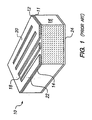
- a reflective deformable grating light modulator 10 As illustrated in Fig. 1.
- This modulator 10 was proposed by Bloom et al., in U.S. Patent No. 5,311,360.
- the modulator 10 includes a plurality of equally spaced apart, deformable reflective ribbons 18 which are suspended above a substrate 16 having reflective surface portions.
- An insulating layer 11 is deposited on the silicon substrate 16. This is followed by the deposition of a sacrificial silicon dioxide film 12 and a low-stress silicon nitride film 14.
- the nitride film 14 is patterned to form the ribbons 18 and portions of the silicon dioxide layer 12 are etched such that the ribbons 18 are held by a nitride frame 20 on an oxide spacer layer 12.
- the modulator is designed such that the thickness of the ribbons 18 and the thickness of the oxide spacer 12 both equal ⁇ 0 /4.
- the grating amplitude of this modulator 10, defined as the perpendicular distance, d, between the reflective surfaces 22 on the ribbons 18 and the reflective surfaces of the substrate 16, is controlled by applying voltage between the ribbons 18 (the reflective surface 22 of the ribbons 16 serves as a first electrode) and the substrate 16 (a conductive film 24 beneath the substrate 16 serves as a second electrode).
- the grating amplitude equals ⁇ 0 /2 and the total path length difference between light reflected from the ribbons and the substrate equals ⁇ 0 , resulting in these reflections adding in phase.
- the modulator 10 reflects light as a flat mirror.
- the undeformed state is illustrated in Fig. 2 with incident and reflected light indicated as 26.
- Adhesion between the ribbons 18 and the substrate 16 during wet processing utilized to create the space below the ribbons 18 and during operation of the modulator 10 has been found to be a problem in these devices.
- Numerous techniques to reduce adhesion have been proposed, including: freeze-drying, dry etching of a photoresist-acetone sacrificial layer, OTS monolayer treatments, use of stiffer ribbons by using shorter ribbons and/or tenser nitride films, roughening or corrugating one or both of the surfaces, forming inverted rails on the underneath of the ribbons, and changing the chemical nature of the surfaces.
- a feature of the mechanical operation of the modulator 10 is hysteresis in the deformation of the ribbons 18 as a function of applied voltage.
- the theorized reason for the hysteresis is that the electrostatic attractive force between the ribbons 18 and the substrate 16 is a non-linear function of the amount of deformation, while the restoring force caused by stiffness and tension of the ribbons 18 is a substantially linear function.
- Fig. 4 illustrates a simulated hysteresis characteristic where the light output (an indirect indicator of the amount of deformation of the ribbons 18) is shown on the vertical axis and the voltage between the ribbons 18 and the substrate 16 is shown on the horizontal axis.
- Bloom et al. in U.S. Patent No. 5,311,360 teach that this latching feature is desirable as it gives the modulator 10 the advantages of active matrix design without the need for active components.
- Bloom et al. Teach that this latching feature is also desirable in low power applications where efficient use of available power is very important. Recognizing the adhesion problem, however, Bloom et al., teach adding small ridges below the ribbons 18 to reduce the contact area and thereby reduce the adhesion problem. Because the substrate of the modulator 10 is used as an optical surface, however, the manufacturing processes for adding small ridges to the surface is complicated by the requirements that the reflecting portions of the substrate 16 be smooth with high reflectivity and be in a plane parallel to the ribbons 18.
- U.S. Patent 5,757,536 (Ricco et al) describes a light modulator for modulating an incident beam of light specifically constructed or an electrically programmable diffraction grating.
- the light modulator comprises a plurality of elongated elements, each having an approximately flat reflective surface disposed between the two ends, the elements being arranged parallel to each other and suspended by their respective ends above a substrate; and reflective portions of the elongated elements being selectively deformable toward the substrate to enter a deformed state to diffract light without contacting the substrate.
- One aspect of the present invention provides a light modulator as defined above which is characterised by a reflective element disposed over the two ends of each of the plurality of elongated elements in a plane parallel to the reflective surfaces of undeformed elements by a distance equal to a whole number (including zero) multiplied by half the given wavelength.
- the reflective element is disposed in substantially the same plane as the flat center portion of each elongated element in the undeformed state. This equates to selection of the whole number as being zero.
- the provision of the reflective element over the two ends of each elongated elements allows the diffraction of light from other than the approximately flat center portion of each elongated center portion to be prevented from reaching the viewer of the two-dimensional image.
- a light shield is employed to prevent the generation of the two dimensional image resulting from other than light reflected and diffracted by the center portions of the elongated elements.
- the invention also defines a method of generating a two-dimensional image using such a modulator, wherein light from the grating is controlled to prevent generation of the image resulting from other than light reflected and diffracted by th center portions.
- the invention also defines a method of manufacturing such a light modulator.
- the diffraction grating light valve includes a plurality of elongated elements each of which have a reflective surface.
- the elongated elements are suspended substantially parallel to each other above a substrate with their respective ends supported and substantially aligned so as to form a column of adjacent reflecting surfaces (GLV array).
- the elongated elements are grouped according to display elements. Alternate ones of each group are deformable by applying a voltage with respect to the substrate.
- each deformed elongated element is substantially parallel to and a predetermined distance from a center portion of each undeformed element.
- the predetermined distance is selected to be approximately one-third to one-fourth of the distance between the undeformed reflective surfaces and the substrate such that deformed elongated elements do not contact the surface of the substrate. Avoiding contact with the substrate prevents the elongated elements from adhering to the substrate. In addition, limiting the predetermined distance avoids hysteresis in deforming the elongated elements.
- a light beam incident to the column of adjacent reflecting surfaces is reflected from a group of elongated elements when the alternate ones of the group are undeformed.
- the light beam is diffracted by a group of elongated elements when alternate ones of the group are deformed.
- a ratio of between reflection and diffraction for a group during a time period determines a display intensity for the corresponding display element.
- the light beam is alternately red, green and blue during successive periods.
- the light beam is white light and widths of the elongated elements for each display element are selected to diffract red, green or blue wavelengths at an appropriate diffraction angle.
- An appropriate intensity and color for each display element is formed during respective periods according to the image to be represented by the respective display element.
- Light diffracted from the column of reflecting surfaces is collected by a lens.
- the light is columnar and representative of a column of the image to be displayed.
- a light shield having a slit of predetermined width over the length of the column is positioned at the pupil of the second lens such that only a selected portion of the light passes through the slit. This arrangement of the shield prevents light collected by the first lens other than light diffracted from the approximately flat center portions of the elongate elements from passing through the slit.
- a fixed reflecting surface is placed over the ends of the elongated elements to prevent light from being diffracted other than from the approximately flat centre portion of each elongated element.
- a pivotable reflective surface (scanning mirror) is positioned opposite the light shield from the lens to reflect the light passing through the slit into an eyepiece or onto a display screen.
- the reflective surface pivots back and forth, in synchronism with the column of display elements modulating the light, to represent columns of the display image. Accordingly, a two-dimensional color image is swept into the eyepiece or onto the display screen.
- the pivotable scanning mirror can be replaced with other types of mirror arrangements such as a rotating faceted polygon mirror.
- Conventional displays are formed in two dimensional arrays of pixels.
- the discrete image formed by each of the myriad of pixels are integrated by the eye of the user to form a composite of the pixels representing an overall image.
- the cost of such a display system increases because as each pixel is replicated to form the entire array the cost of making each pixel is similarly replicated.
- Examples of such pixellated displays are televisions and computer monitors.
- the pixels for each can be formed of LCD devices, or by a CRT. What is needed is a display that lowers the cost of manufacture by reducing the number of pixels required to build the system without lowering the image quality.
- Figs. 1-4 relate to a prior art reflective grating modulator
- Figs. 5-13 relate to the construction of a light modulator grating for use in the implementation of the present invention
- Figs. 14 and 15 relate to the implementation of the light modulator grating in a display apparatus with a light shield
- Figs. 16 and 17 illustrating further detail of the display apparatus
- Fig. 18 illustrates the application of a reflective member to the light modulator grating in accord with the invention.
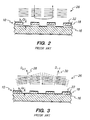
- Figs. 5-6 and 8 illustrate side sectional views of a process sequence for manufacturing a columnar diffraction grating light valve (GLV) for use in the implementation of the present invention.
- an insulating layer is formed on a silicon substrate 100.
- the insulating layer is a composite layer including a field oxide layer 102 formed by thermal oxidation and a thin layer of silicon nitride 104 formed over the field oxide layer 102.
- the conducting layer 106 is a refractory metal, such as tungsten, molybednum, titanium-tungsten or tantalum or alternatively conductive Poly-silicon or a diffused conductor.
- the conducting layer 106 serves as a lower electrode for applying bias to selected ones of elongated elements of the GLV.
- the conducting layer 106 is formed on a lower surface of the substrate 100.
- a sacrificial layer 108 is formed over the conducting layer 106.
- the sacrificial layer 108 must be able to be selectively etched with respect to the conducting layer 106.
- the sacrificial layer 108 is a layer of Poly-silicon which is etched with a dry etch of xenon diflouride.
- the sacrificial layer can be a layer of doped glass, such as boro-phospho-silicate glass or phoso-silicate glass.
- the thickness at which the sacrificial layer 108 is applied determines a distance between the conducting layer 106 and elongated elements to be formed over the sacrificial layer 108.
- the thickness of the sacrificial layer 108 departs significantly from prior light modulators in that the sacrificial layer 108 is substantially thicker.
- the thickness of the sacrificial layer 108 is approximately equal to the expected wavelength of incident light. For example, if the expected wavelength is in the visible range (approximately 450-760 nm), the thickness of the sacrificial layer 108 is also within this approximate range. If the expected wavelength is in the ultraviolet range (approximately 200-450 nm) the thickness of the sacrificial layer 108 is also within this approximate range. If the expected wavelength is in the infrared range (approximately 760-2000 nm) the thickness of the sacrificial layer 108 is also within this approximate range.
- the conducting layer 106 and the sacrificial layer 108 are photo-lithographically masked by known techniques and then etched sequentially by appropriate dry or wet etch chemistries, forming a pair of post holes 110 for each elongated element of the GLV.
- the post holes 110 are formed at distance of approximately 75 microns from each other, though another distance can be utilized.
- the apparent thicknesses of the layers 102-108 are exaggerated relative the distance between the post holes 110.
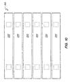
- Fig. 7 illustrates a top view of the GLV after the post holes 110 have been etched as described above.
- Fig. 7 illustrates a column of six pairs of post holes 110, each pair corresponding to an elongated element of the GLV.
- the GLV includes more pairs of post holes 110.
- 1920 pairs of post holes 110 can be utilized corresponding to 1920 elongated elements arranged in a columnar array.
- a layer of resilient material 112 is formed over the sacrificial layer 108 and post holes 110, partially or completely filling the post holes 110.
- the resilient material 112 is layer of silicon nitride deposited to a thickness and residual stress defined by a spring force necessary to return each elongated element to an up state after a sufficient opposite polarity bias is applied to cancel electrostatic force induced by a bias applied to place the elongated element in a down state.
- a reflective layer 114 is deposited over the resilient layer 112.
- the reflective layer 114 provides a reflective surface for each elongated element of the GLV and serves as an upper electrode for applying bias to selected ones of the elongated elements of the GLV.
- the reflective layer 114 is sputtered aluminum.
- a photoresist layer 118 is applied as a mask for selectively patterning the reflective layer 114 and the resilient layer 112 for forming the elongated elements.
- the sacrificial layer 108 is etched, leaving an air space beneath the elongated elements.
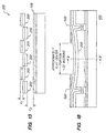
- Fig. 9 illustrates a side sectional view of an elongated element 200 of the GLV in an undeformend state. Note that in Fig. 9, the sacrificial layer 108 (Figs. 5-6 and 8) beneath, the elongated element 200 is replaced by an air space 202. Thus, the elongated element 200 is suspended by its ends above the surface of the substrate (including its constituent layers). In addition, the photoresist layer 118 (Fig. 8) has been removed.
- Fig. 10 illustrates a top view of a portion of the GLV including six elongated elements 200.
- the elongated elements 200 have equal widths and are arranged parallel to each other.
- the elongated elements 200 are also separated from each other by a small space, thus, allowing each elongated element 200 to be selectively deformed with respect to the others.
- the six elongated elements 200 illustrated in Fig. 10 preferably correspond to a single display element 300.
- the column of 1920 elongated elements corresponds to a GLV array having 320 display elements arranged in a column. It will be apparent that the number of display elements will affect a resulting display resolution and that a different number can be selected.
- each display element 300 can have a different number of elongated elements 200.
- a group of two, four, eight, ten or twelve elongated elements 200 can correspond to a single display element 300. It is possible that even more elongated elements could be used to form a single display element 300. It is also possible that an odd number of elongated elements 200 could be used for a single display element 300.
- Fig. 11 illustrates a front sectional view of the display element 300 with the elongated elements 200 undeformed.
- the section illustrated in Fig. 11 is taken along the line A-A' illustrated in Fig. 9.
- the undeformed state is achieved by equalizing a bias on each elongated element 200 with respect to the conductive layer 106. Note that because the reflective surfaces of the elongated elements 200 are substantially co-planar, light incident to the elongated elements 200 is reflected.
- Fig. 12 illustrates a side sectional view of a deformed elongated element 200 of the GLV.
- Fig. 12 illustrates that in the deformed state, the elongated element 200 remains suspended in that it does not come into contact with the surface of the substrate layers beneath the elongated element 200. This is in contrast to the prior modulator of Figs. 1-3. By avoiding contact between the elongated element 200 and surface of the substrate, the problem of adhesion associated with the prior modulator is avoided. Note, however, that in the deformed state, the elongated element 200 tends to sag. This is because the electrostatic force pulling the elongated element 200 toward the substrate is distributed.
- a center portion 202 (Fig. 12) of the elongated elements 200 remains approximately flat, such that a contrast ratio resulting from obtaining light diffracted only by the center portion 202 of each elongated element 200 is satisfactory.
- the approximately flat center portion 202 is approximately one-third the length between the post holes 110. Therefore, when the distance between post holes is 75 microns, the approximately flat center portion 202 is approximately 25 microns in length.
- Fig. 13 illustrates a front sectional view of the display element 300 with alternate ones of the elongated elements 200 deformed.
- the section illustrated in Fig. 13 is taken along the line B-B' illustrated in Fig. 12.
- the elongated ribbons 200 that are not moved substantially are held in a desired location by applying a bias voltage thereto.
- the deformed state in the elongated ribbons 200 that move is achieved by applying an appropriate drive voltage on the alternate ones of the elongated elements 200 with respect to the conductive layer 106.
- the perpendicular distance d 1 is approximately constant over the approximately flat center portion 202 (Fig. 12) and, thus, defines a grating amplitude for the GLV.
- the grating amplitude d 1 can be adjusted by adjusting the drive voltage on the driven elements elongated 200. This makes possible fine tuning of the GLV for an optimum contrast ratio.
- each deformed elongated element 200 is separated from the surface of the substrate by a distance d 2 .
- This distance d 2 is preferably selected to be approximately two to three times the distance d 1 . Accordingly, in the deformed state, the elongated elements 200 travel approximately one-fourth to one-third of the distance d 2 to the substrate.
- the distance d 2 is determined by the thickness of the sacrificial layer 108 (Figs. 5-6 and 8) plus the distance d 1 .
- hysteresis curve illustrated in Fig. 4 because the elongated elements 200 diffract the incident light by traveling only one-third to one-fourth of the distance to the surface of the substrate, hysteresis is avoided. Instead, starting from the undeformed state, the elongated elements 200 deform toward the substrate and, then, return to the undeformed state along the same voltage versus light intensity curve in each direction of travel. This is in contrast to the prior modulator illustrated in Figs. 1-3 which encounters hysteresis when deforming to into diffracting state. This embodiment allows a continuous selection of the brightness by varying the drive voltage in a continuous manner on the driven elongated elements 200.
- each elongated element 200 Because the end portions of each elongated element 200 are not approximately flat, if light diffracted by the end portions is collected and displayed, the resulting contrast ratio of the display image will tend to be unsatisfactory. Therefore, as explained in one embodiment of herein, the present invention a light shield is provided for preventing light diffracted from other than the approximately flat center portion 202 of each elongated element 200 from being utilized for forming the display image. In the alternative, the light could be optically manipulated so that it only impinges onto the approximately flat center portion 202. This approach avoids wasting light.
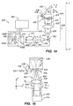
- Fig. 14 illustrates top view of an optical display system 400 utilizing the GLV array 402.
- An illumination arrangement for illuminating the GLV array 402 includes red, green, and blue light sources 404R, 404G and 404B, respectively.
- These light sources can be any convenient source of red, green and blue light and can be semiconductor light emitting devices such as light emitting diodes (LEDs) or semiconductor lasers, or separate diode pumped solid state lasers, or white fight with alternating filters such as a spinning disk with three filters to sequentially pass red, green and blue light.
- LEDs light emitting diodes
- 404B separate diode pumped solid state lasers
- white fight with alternating filters such as a spinning disk with three filters to sequentially pass red, green and blue light.
- light sources 404R, 404G, and 404B are assumed to be sources emitting in a generally symmetrical manner.
- a dichroic filter group 406 allows light from any one of these light sources to be directed toward a collimating lens 408 propagating generally along a system optical axis z.
- Dichioic filter groups or prism blocks which cause three light sources of different color to appear to an optical system to emanate from the same point of origin are well known in the optical art, for example, Philips prisms. Accordingly, a detailed description of such dichroic filter groups is not presented herein.
- the system of the present invention could also comprise three display engines which, are combined and then scanned to form a composite image.
- the GLVs are formed using semiconductor processing techniques, it is possible to form three parallel linear arrays that are essentially perfectly aligned one to the other.
- Three illumination systems, one each for red, green and blue can be configured to impinge their respective color of light onto a single one of the three essentially perfectly aligned GLV linear arrays. In this way, alignment of the composite image is easier than for conventional composite color systems.
- color break up This results from such systems displaying a red frame, a green frame and a blue frame, in any convenient sequence. This technique is known as frame sequential color. If an object passes between the viewer and the displayed image a ghost of that object in one of the colors will appear in the display. Similarly, if the viewer quickly turns their head an artifact of the frame sequential color will appear.
- the system can be made to operate to provide each of the three display colors for each row of the display as it is scanned.
- the inventors have coined the phrase 'line sequential color' to describe this technique. The deleterious artifacts of frame sequential color are not present.
- the image is formed by scanning a linear array of GLVs.
- the elongated elements in the linear array are all parallel and perpendicular to the length of the linear array. This avoids any discreetly displaying of adjacent elements.
- adjacent display elements such as is present in conventional LCD or CRT displays.
- the array is smoothly scanned in a direction perpendicular to the linear array, there can be no pixellation between the display in that direction either. In this way, the image quality is vastly improved over that of conventional display technologies.
- Lens 408 is illustrated, for simplicity as a simple "spherical" lens, i.e having equal refractive power in then x and y axes.
- the y axis is in the plane of the illustration and the x axis is perpendicular to the plane of the illustration.
- the lens 408 collimates light from the light source in both axes.
- Those familiar with the art to which the present invention pertains will recognize however, that light output from an end-emitting semiconductor laser is more divergent in one transverse (x or y) axis than the other and is astigmatic.
- Means for collimating the output beam of such a laser and expanding it to a desired size are well-known in the optical art and may require one or more spherical, aspherical, toroidal, or cylindrical (spherical and aspherical) lens elements.
- Lens 408 is intended to represent a group of one or more such elements.
- Divergent light 410 from a symmetrically emitting light source 404 passes through lens 408 and is collimated in both the x and y axes.
- Bi-axially collimated light 412 is then passed through a cylindrical lens 414.
- the function of lens 414 is to cause bi-axially collimated light 412 passing therethrough to converge (Fig. 14, lines 416) in the y axis, and remain collimated (Fig. 15 lines 418) in the x axis.
- lens 414 may also be formed from one or more optical elements as discussed above, and is shown as a single element for simplicity.
- GLV array 402 is located at a distance from cylindrical lens 414 of about a focal length (f 1 ) of the lens. GLV array 402 is aligned in the x axis, on the system optical axis z which corresponds to the optical axis of lenses 408 and 414.
- the operating surface of the GLV (elongated elements 200) is inclined to the z axis.
- GLV array 402 is inclined as 45 degrees to the axis, which effectively folds the z axis 90 degrees. This selection of inclination of the GLV array 402 is made here for convenience of illustration and should not be considered limiting.
- Fig. 15 illustrates a side view of the optical display system illustrated in Fig. 14 taken along the line C-C.
- light incident on an operating GLV array 402 creates a reflected beam (418) and plus and minus first-order diffracted beams designated by D +1 and D -1 respectively. These diffracted beams are inclined to the z axis, in the x axis. In the y axis, the diffracted and reflected beams are equally divergent.
- the diffracted and reflected beams then pass through a magnifying (positive) lens 420 which is separated from GLV array 402 by a focal length f 2 of the lens.
- Lens 420 is shown as a single element from simplicity, but in practice lens 420 may include two or more elements.
- Lens 420 provides in effect an eyepiece lens for system 400 and is preferably one of the well-known group of eyepiece lens types, consisting of Huygens, Ramsden, Kellner, Plössel, Abbe, König, and Erfle types.
- the reflected beam 422 converges to a focal point on the z axis, at which is placed an elongated stop 424 at about an external telecentric exit pupil P 2 of lens 420.
- a shield 426 is placed in the area of the pupil P 2 of lens 420 to shield light diffracted from portions of the elongated elements 200 of the GLV array 402 other than light diffracted from the approximately flat center portion 202 of each-elongated element.
- the shield has a slit that is preferably dimensioned so as to only pass light (D +1 , D -1 ) diffracted from the approximately 25 micron center portion 202 of each elongated element 200.
- the Schlieren optics of system 400 can be defined as being a part of a telecentric optical arrangement 428 including GLV array 402 magnifying eyepiece lens 420 and stop 424, with GLV array 402 at about an external object position of lens 420 and stop 424 at about an external (exit) pupil of lens 420.
- a telecentric system is a system in which the entrance pupil and/or the exit pupil is located at infinity. It is widely used in optical systems designed for metrology because it tends to reduce measurement or position error caused by slight defocusing of the system. This tendency permits some tolerance in placement of stops and other components of the system in general, and is exploited m certain embodiments of the present invention discussed further hereinbolow.
- divergent reflected fight 430 (and diffracted light) is collimated by lens 420.
- Stop 424 is aligned in the y axis, and intercepts the reflected light.
- Shield 426 absorbs diffracted light other than light diffracted from the approximately flat center portions 202 of the GLV array 402. Stop 424 may be selected to be absorbing or reflecting. If stop 424 is reflecting, reflected light from is returned to GLV array 420.
- Diffracted beams D +1 and D -1 being inclined to the z axis and the corresponding incident and reflected beams, converge to focal points about and below (alternatively, on opposite sides of) stop 424 and with the slit of shield 426, thereby passing through exit pupil P 2 without being intercepted.
- a scanning mirror 432 is located such as to intercept the diffracted beams and direct them toward a viewer's eye 434. What the viewer sees is a magnified virtual image (at infinity) of GLV array 402. This image is represented to Fig. 5 by line 436, recognizing, of course, that there is no real image here. It will be apparent that the line of the GLV array 402 can represent a row or a column of an image to be displayed. The appropriate remaining rows or columns are then formed as the scan progresses. It is possible that other scanning modes can be used, suoh as diagonally.
- the elongated elements 200 of GLV array 402 are operated to represent, sequentially, different lines of M x N display where M is the number of display elements per line, and N is the number of lines in the display.
- Each display element 300 includes multiple elongated elements 200, as discussed above.
- GLV array 402 may be defined generally as representing, a one-dimensional array of light valves, or one row of display elements or pixels. In the magnified virtual image, these pixels will have a relative brightness determined by the operating state of ribbon or ribbons 12 of GLV array 10
- Scanning mirror 432 is moved, angularly, by a drive unit 436 about an axis 438 as illustrated by arrow A (Fig.14), scanning the diffracted beams, and thus the magnified virtual image, linearly, across the field of view of the viewer, as indicated by arrow B, to represent sequential lines of the display.
- Mirror 432 is moved fast enough to cause the scanned virtual image to appear as a two-dimensional image to the viewer.
- the pivotable scanning mirror 432 can be replace with other types of mirror arrangements such as a rotating faceted polygon mirror.
- Microprocessor-based electronic control circuitry 440 is arranged to accept video data and is coupled to GLV array 402 for using the video data to operate the elongated elements 200 of the GLV array 402 for modulating light diffracted therefrom.
- the circuitry 440 is arranged such that the light in diffracted beams D +1 and D -1 , is modulated to represent sequential lines of a two-dimensional image representing the video data, as noted above.
- Control circuitry 440 is also coupled to scanning mirror drive unit 436 to synchronize the display of sequential lines and to provide that sequential frames of the image begin at an extreme of the angular excursion range of scanning mirror 432.
- the speed of the scanning can be controlled to be sinusoidal, saw toothed or any other convenient speed algorithm. All that is necessary is that the scanning speed be synchronized with the presentation of the data to the GLV array 402.
- Control circuitry 432 is also coupled to light sources 404R, 404G, and 404B for switching the sources sequentially, cooperative with operation of GLV may 402 to provide sequential red, green and blue resolution image of the array, which, together, represent one resolution line of colored two-dimensional image.
- the elongated members 200 of each display element 300 are appropriately modulated while each of the light sources 404R, 404G and 404B are sequentially active to provide as appropriate proportion of each of red, green and blue diffracted light for the display element 300 while the corresponding line of the image is displayed to the viewer. This modulation occurs at a rate that is sufficiently high that the viewer perceives an appropriate combined color for each display element 300.
- light sources 404R, 404G and 404B are activated simultaneously to illuminate GLV array 402 and two additional arrays (not shown) via a dichroic prism block (not shown) placed between lens 420 and the three GLV arrays Each GLV array would then be arranged to modulate a particular one of the three primary color components red, green, and blue of the image.
- the dichroic prism block may be of any well-known type for example an above mentioned Phillips prism block, and would in this case be arranged such that each GLV array appeared to be located at the same distance from, and inclination, to, lens 420.
- light sources 404R, 404G and 404B could be replaced by a single white light source, and dichroic prism block 406 omitted.
- viewer's eye 434 is illustrated in a less than ideal position for properly viewing a magnified virtual image of the display of system 400.
- the viewer's eye should be located at about exit pupil P 2 .
- mirror 432 which is preferably also located at about this exit pupil.
- This difficulty can be overcome by optically relaying an image of the exit pupil away from the mirror, to a position at which it is easy to locate a viewers eye, thereby allowing the scanning mirror 432 and the viewer's eye each to be located at about a pupil position.
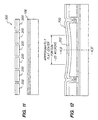
- Fig. 16 One means of relaying an image of exit pupil P 2 is illustrated in Fig. 16 wherein the optical arrangement is shown as optically "unfolded" with scanning mirror 432 represented as a line at exit pupil P 2 of lens 420, that being one preferred position for the scanning mirror 432.
- shield 426 is placed is the area of the pupil P 2 .
- pupil-relaying is accomplished by two lenses 442 and 444 of the same focal length, which are spaced apart by a distance equal to twice that focal length to form a unit magnification telecentric relay which places an image P 3 of exit pupil P 2 a focal length of lens 444 away from the lens 444, providing adequate eye-relief from lens 444.
- lenses 442 and 444 may include more than one lens element, and further, that the telecentric relay arrangement illustrated in Fig. 16 is not the only possible optical arrangement for relaying a pupil image.
- Fig. 17 where again the optical system is illustrated as "unfolded” with scanning mirror 432 represented as a line at exit pupil P 2 of lens 420, that being, here also, one preferred position for the scanning mirror 432).
- Shield 426 is also placed in the area of the pupil P 2 .
- Eyepiece lens 420 may also be used as one element, or group of elements, for projecting a magnified real image of the GLV array 402 on a screen or on a recording medium, such as would be required to provide a projection display or a device for recording or printing an image.
- a lens (or group of lens elements) 446 is positioned to focus a magnified real image 448 (here, the width) of GLV array 402 at a finite distance from lens 446.
- This image could be focussed in a plane 450 which could be a viewing screen for providing a projected (apparent) two-dimensional image, or on a recording medium such a photographic film or paper.
- scan mirror 432 could be eliminated, and scanning achieved by moving a recording or printing medium in the scan direction, which, in Fig. 17 is perpendicular to the plane of the illustration, i.e., perpendicular to the orientation of the image.
- This mechanical scanning motion would, of course, need to be synchronized with image generation by electric circuitry 440 as in system 400.
- a reflective element 500 is disposed over the outermost portions of each elongated element 200.
- a side sectional view of such a reflective element 500 is illustrated in Fig. 18 disposed over a deformed elongated element 200.
- the approximately flat center portion 202 (Fig. 12) of the elongated element 200 remains exposed to incident light while the outer portions are covered by the reflective element 500.
- the reflective element 500 reflects incident light.
- the reflective element 500 illustrated in Fig. 18 is preferably sufficiently thin that it is in substantially the same plane as the approximately flat center portion 202 of each elongated element 200 (in the undeformed state).
- the embodiment described principally above is for forming a display for human viewing.
- Other types of 'displays' are also contemplated within the present invention.
- an image could be formed on a rotating drum for transfer to paper in a printing process.
- the light source could also be ultraviolet or infrared. Such an image is not visible to a human but is equally useful.
Abstract
Description
reflective portions of the elongated elements being selectively deformable toward the substrate to enter a deformed state to diffract light without contacting the substrate.
Claims (29)
- A modulator for modulating an incident beam of light having a given wavelength, the modulator comprising :characterised bya plurality of elongated elements (200), each having an approximately flat reflective surface disposed between two ends, the elements being arranged parallel to each other and suspended by their respective ends above a substrate (100); andreflective portions of the elongated elements being selectively deformable toward the substrate to enter a deformed state to diffract light without contacting the substrate;
a reflective element (500) disposed over the two ends of each of the plurality of elongated elements (200) in a plane parallel to the reflective surfaces of undeformed elongated elements by a distance equal to a whole number (including zero) multiplied by half the given wavelength. - The modulator according to Claim 1 further comprising control circuitry for applying a modulation voltage to selected ones of the elongated elements to move said selected ones to a deformed state.
- The modulator of Claim 1 or 2, wherein the elongated elements are grouped according to a plurality of modulatable display elements arranged in a single linear array, and are coupled to an optical arrangement for displaying an image according to a respective intensity provided by each display element.
- The modulator according to Claim 3 further comprising an optical arrangement for scanning an image from the single linear array to form a two dimensional image.
- The modulator according to Claim 4 further comprising means for sequentially illuminating the plurality of elongated elements with a plurality of wavelengths related to different colors of light such that the two dimensional image is formed without color break up.
- The modulator according to Claim 4 or 5 wherein the two- dimensional image is not pixellated.
- The modulator according to Claim 2 and any one of Claims 3 to 6 wherein the distance of movement of the selected ones of the elongated elements determines an intensity for the corresponding display element.
- The modulator according to Claim 2 and any one of Claims 3 to 6 wherein a ratio of a period of reflection to a period of diffraction determines an intensity for a display element.
- The modulator of any preceding claim, wherein the plurality of the elongated elements are suspended by their respective ends by integrally formed posts (110) above a substrate, the posts being integrally formed to the elongated elements and the substrate.
- The modulator according to any preceding claim wherein said given wavelength is in a range of wavelengths of an incident beam of light which the modulator is capable of modulating.
- The modulator according to claim 10 wherein the given wavelength is within a range of visible light wavelengths.
- The modulator according to Claim 10 wherein the given wavelength is within a range of ultraviolet light wavelengths.
- The modulator according to Claim 10 wherein the given wavelength is within a range of infrared light wavelengths.
- The modulator according to Claim 2 wherein said means is operable to move the reflective portion of a selected elongated element to the deformed state by approximately one-fourth of the given wavelength.
- The modulator according to Claim 2 wherein said means is operable to move the respective reflective portions of the selected ones of the elongated elements a controllable distance to provide a desired brightness of modulated light.
- The modulator according to any one of Claims 1-13 wherein the grating amplitude of said reflective portions of the elongated elements is approximately one-fourth to one-third of the distance between undeformed elongated elements and the substrate.
- The modulator according to any preceding claim wherein the reflective portion of each elongated element comprises approximately one-third of the length of the element.
- A modulator according to any preceding claim in which the reflective portion of each elongated element comprises a center portion of the element.
- A modulator for modulating an incident beam of light having a given wavelength, the modulator comprising:characterised bya plurality of elongated elements (200), each having an approximately flat reflective surface disposed between two ends, the elements being arranged parallel to each other and suspended by their respective ends above a substrate (100); andreflective portions of the elongated elements being selectively deformable toward the substrate to enter a deformed state to diffract light without contacting the substrate;
the elongated elements being grouped according to a plurality of display elements arranged in a single linear array, and being coupled to an optical arrangement for displaying an image resulting from modulation of the display elements, said optical arrangement comprising a light shield for preventing light diffracted by other than said reflective portions of the elongated elements from being displayed in the image. - The modulator according to Claim 19 wherein the shield comprises a slit for passing light diffracted by the approximately flat center portions of the elongated elements.
- The modulator according to Claim 19 or 20 wherein the optical arrangement is configured for projecting an image onto a print medium.
- A method of forming a light modulator for modulating an incident beam of light having a given wavelength, the method characterised by the steps of:a. providing a substrate (100)b. forming a sacrificial layer (108) on the substrate (100), wherein the sacrificial layer (108) has a thickness that is approximately equal to the given wavelength;c. forming posts (110) through the sacrificial layer 108 and into the substrate (100);d. forming at least two elongated elements over the sacrificial layers, each elongated element having a reflective surface and each elongated element being coupled to the substrate by two of the posts, one at each end of each elongated element;e. removing the sacrificial layer; andf. disposing reflective elements over the two ends of each of the plurality of elongated elements in a plane parallel to the reflective surfaces of the elongated elements and spaced therefrom by a distance equal to a whole number (including zero) multiplied by half the given wavelength.
- The method according to Claim 22 wherein the thickness of the sacrificial layer is within a range of 200 to 2000 nm for forming a light modulator for modulating visible light.
- An optical system for displaying an image comprising:a. a plurality of elongated elements, each element having an approximately flat reflective surface disposed between two ends, the elements arranged parallel to each other and suspended by their respective ends above a substrate, the elongated elements grouped according to a plurality of display elements arranged in a single linear array;b. means for deforming selected ones of the elongated elements toward the substrate thereby entering a deformed state wherein the approximately flat reflective surface of each selected element moves toward the substrate by a grating amplitude without the selected elongated elements contacting the substrate such that when the elongated elements corresponding to a display element are undeformed, an incident beam of light is reflected by the display element, and further such that when alternate ones of elongated elements corresponding to the display element are selectively deformed, the incident beam of light is diffracted by the display element, wherein a distance of movement of the selected ones of the elongated elements determines an intensity for the corresponding display element;c. an optical arrangement for forming the image according to a respective intensity formed by each display element; andd. a reflective element disposed over the two ends of each elongated element in a plane parallel to the reflective surfaces of undeformed elongated elements by distance equal to a whole number (including zero) multiplied by half the wavelength of the incident beam of light.
- The optical system of Claim 24, wherein the plurality of the elongated elements are suspended above the substrate at their respective ends by integrally formed posts.
- A method for generating a two-dimensional image using a light modulator comprising a grating having a plurality of elongated elements, each element having an approximately flat reflective surface disposed between two ends, the elements arranged parallel to each other and suspended by their respective ends above a substrate, the elongated elements grouped according to a plurality of display elements arranged in a single linear array, the method comprising the steps ofa. deforming selected ones of the elongated elements toward the substrate to enter a deformed state wherein the approximately flat reflective surface of each selected element moves toward the substrate by a grating amplitude without the selected elongated elements contacting the substrate such that when the elongated elements corresponding to a display element are undeformed, an incident beam of light is reflected by the display element, and further such that when alternate ones of elongated elements corresponding to the display element are selectively deformed, the incident beam of light is diffracted by the display element, wherein a distance of movement of the selected ones of the elongated elements determines an intensity for the corresponding display element; and characterised by the step ofb. controlling light from the grating used to generate the two dimensional image so as to prevent the generation of the image resulting from other than light reflected and diffracted by the center portions of the elongated elements.
- The method of Claim 26, wherein the controlling of light from the grating is accomplished with reflective elements disposed over the two ends of each elongated element in a plane parallel to the reflective surfaces of undeformed elongated elements and at a distance therefrom equal to a whole number (including zero) multiplied by half the wavelength of the incident beam of light.
- The method of Claim 26, wherein the controlling of light from the grating is accomplished with a slitted shield that blocks the light modulated adjacent the ends of the elongated elements.
- The method of Claim 26 or, 27 or 28, wherein the plurality of the elongated elements are suspended above the substrate by their respective ends through integrally formed posts.
Applications Claiming Priority (3)
| Application Number | Priority Date | Filing Date | Title |
|---|---|---|---|
| US09/104,159 US6215579B1 (en) | 1998-06-24 | 1998-06-24 | Method and apparatus for modulating an incident light beam for forming a two-dimensional image |
| US104159 | 1998-06-24 | ||
| PCT/US1999/013955 WO1999067671A1 (en) | 1998-06-24 | 1999-06-18 | Method and apparatus for modulating an incident light beam for forming a two-dimensional image |
Publications (2)
| Publication Number | Publication Date |
|---|---|
| EP1090322A1 EP1090322A1 (en) | 2001-04-11 |
| EP1090322B1 true EP1090322B1 (en) | 2003-03-05 |
Family
ID=22298956
Family Applications (1)
| Application Number | Title | Priority Date | Filing Date |
|---|---|---|---|
| EP99930488A Expired - Lifetime EP1090322B1 (en) | 1998-06-24 | 1999-06-18 | Method and apparatus for modulating an incident light beam for forming a two-dimensional image |
Country Status (10)
| Country | Link |
|---|---|
| US (1) | US6215579B1 (en) |
| EP (1) | EP1090322B1 (en) |
| JP (1) | JP2002519714A (en) |
| KR (1) | KR20010053201A (en) |
| CN (1) | CN1313957A (en) |
| AT (1) | ATE233911T1 (en) |
| AU (1) | AU4702199A (en) |
| CA (1) | CA2335584A1 (en) |
| DE (1) | DE69905717T2 (en) |
| WO (1) | WO1999067671A1 (en) |
Cited By (2)
| Publication number | Priority date | Publication date | Assignee | Title |
|---|---|---|---|---|
| DE102006041875A1 (en) * | 2006-09-01 | 2008-03-13 | Seereal Technologies S.A. | Holographic projection system with micromirrors for light modulation |
| US9372472B2 (en) | 2013-03-11 | 2016-06-21 | Christie Digital Systems Usa, Inc. | System for order alignment of diffractively produced images |
Families Citing this family (115)
| Publication number | Priority date | Publication date | Assignee | Title |
|---|---|---|---|---|
| EP2332645A1 (en) * | 1998-02-11 | 2011-06-15 | The University Of Houston | Apparatus for chemical and biochemical reactions using photo-generated reagents |
| US20040035690A1 (en) * | 1998-02-11 | 2004-02-26 | The Regents Of The University Of Michigan | Method and apparatus for chemical and biochemical reactions using photo-generated reagents |
| US6271957B1 (en) * | 1998-05-29 | 2001-08-07 | Affymetrix, Inc. | Methods involving direct write optical lithography |
| US6303986B1 (en) | 1998-07-29 | 2001-10-16 | Silicon Light Machines | Method of and apparatus for sealing an hermetic lid to a semiconductor die |
| US6337753B1 (en) * | 1998-12-21 | 2002-01-08 | Lucent Technologies Inc. | Optical power equalizer |
| US6724125B2 (en) | 1999-03-30 | 2004-04-20 | Massachusetts Institute Of Technology | Methods and apparatus for diffractive optical processing using an actuatable structure |
| DE19941045A1 (en) * | 1999-08-28 | 2001-04-12 | Bosch Gmbh Robert | Micro vibrating device |
| US6826330B1 (en) | 1999-08-11 | 2004-11-30 | Lightconnect, Inc. | Dynamic spectral shaping for fiber-optic application |
| US6501600B1 (en) | 1999-08-11 | 2002-12-31 | Lightconnect, Inc. | Polarization independent grating modulator |
| US6674563B2 (en) | 2000-04-13 | 2004-01-06 | Lightconnect, Inc. | Method and apparatus for device linearization |
| JP4474000B2 (en) * | 2000-01-20 | 2010-06-02 | キヤノン株式会社 | Projection device |
| US6307663B1 (en) * | 2000-01-26 | 2001-10-23 | Eastman Kodak Company | Spatial light modulator with conformal grating device |
| US6888983B2 (en) | 2000-04-14 | 2005-05-03 | Lightconnect, Inc. | Dynamic gain and channel equalizers |
| US6611377B1 (en) * | 2000-07-10 | 2003-08-26 | Intel Corporation | Micromechanical diffraction phase grating |
| US6411425B1 (en) * | 2000-09-27 | 2002-06-25 | Eastman Kodak Company | Electromechanical grating display system with spatially separated light beams |
| US6556338B2 (en) * | 2000-11-03 | 2003-04-29 | Intpax, Inc. | MEMS based variable optical attenuator (MBVOA) |
| JP2002162599A (en) * | 2000-11-24 | 2002-06-07 | Sony Corp | Stereoscopic image display device |
| US6624880B2 (en) | 2001-01-18 | 2003-09-23 | Micronic Laser Systems Ab | Method and apparatus for microlithography |
| SE0100336L (en) | 2001-02-05 | 2002-08-06 | Micronic Laser Systems Ab | Addressing method and apparatus using the same technical area |
| US6567584B2 (en) | 2001-02-12 | 2003-05-20 | Silicon Light Machines | Illumination system for one-dimensional spatial light modulators employing multiple light sources |
| US20020167695A1 (en) * | 2001-03-02 | 2002-11-14 | Senturia Stephen D. | Methods and apparatus for diffractive optical processing using an actuatable structure |
| US6614580B2 (en) * | 2001-04-10 | 2003-09-02 | Silicon Light Machines | Modulation of light out of the focal plane in a light modulator based projection system |
| US6707591B2 (en) | 2001-04-10 | 2004-03-16 | Silicon Light Machines | Angled illumination for a single order light modulator based projection system |
| US6639724B2 (en) * | 2001-06-05 | 2003-10-28 | Lucent Technologies Inc. | Device having a barrier layer located therein and a method of manufacture therefor |
| US6782205B2 (en) | 2001-06-25 | 2004-08-24 | Silicon Light Machines | Method and apparatus for dynamic equalization in wavelength division multiplexing |
| US6646778B2 (en) | 2001-08-01 | 2003-11-11 | Silicon Light Machines | Grating light valve with encapsulated dampening gas |
| US6639722B2 (en) * | 2001-08-15 | 2003-10-28 | Silicon Light Machines | Stress tuned blazed grating light valve |
| US6785001B2 (en) | 2001-08-21 | 2004-08-31 | Silicon Light Machines, Inc. | Method and apparatus for measuring wavelength jitter of light signal |
| US7046410B2 (en) | 2001-10-11 | 2006-05-16 | Polychromix, Inc. | Actuatable diffractive optical processor |
| US6692129B2 (en) | 2001-11-30 | 2004-02-17 | Silicon Light Machines | Display apparatus including RGB color combiner and 1D light valve relay including schlieren filter |
| US6800238B1 (en) | 2002-01-15 | 2004-10-05 | Silicon Light Machines, Inc. | Method for domain patterning in low coercive field ferroelectrics |
| US6665048B2 (en) | 2002-01-22 | 2003-12-16 | Creo Inc. | Method for imaging a continuously moving object |
| US7221512B2 (en) | 2002-01-24 | 2007-05-22 | Nanoventions, Inc. | Light control material for displaying color information, and images |
| JP3558066B2 (en) * | 2002-02-19 | 2004-08-25 | ソニー株式会社 | MEMS element and its manufacturing method, light modulation element, GLV device and its manufacturing method, and laser display |
| AU2003230610A1 (en) * | 2002-03-08 | 2003-09-22 | Trustees Of Boston University | Method for linearizing deflection of a mems device using binary electrodes and voltage modulation |
| US20030184531A1 (en) * | 2002-03-29 | 2003-10-02 | Sony Corporation | GLV engine for image display |
| US6947198B2 (en) * | 2002-03-29 | 2005-09-20 | Sony Corporation | Emissive image display apparatus |
| US6987240B2 (en) * | 2002-04-18 | 2006-01-17 | Applied Materials, Inc. | Thermal flux processing by scanning |
| US6767751B2 (en) | 2002-05-28 | 2004-07-27 | Silicon Light Machines, Inc. | Integrated driver process flow |
| US6728023B1 (en) | 2002-05-28 | 2004-04-27 | Silicon Light Machines | Optical device arrays with optimized image resolution |
| US6822797B1 (en) | 2002-05-31 | 2004-11-23 | Silicon Light Machines, Inc. | Light modulator structure for producing high-contrast operation using zero-order light |
| US6804038B1 (en) | 2002-06-26 | 2004-10-12 | Silicon Light Machines, Inc. | Bipolar operation of light-modulating array |
| US6898377B1 (en) | 2002-06-26 | 2005-05-24 | Silicon Light Machines Corporation | Method and apparatus for calibration of light-modulating array |
| US7053930B2 (en) * | 2002-06-27 | 2006-05-30 | Silicon Light Machines Corporation | Triangular bidirectional scan method for projection display |
| US6813059B2 (en) | 2002-06-28 | 2004-11-02 | Silicon Light Machines, Inc. | Reduced formation of asperities in contact micro-structures |
| US6714337B1 (en) | 2002-06-28 | 2004-03-30 | Silicon Light Machines | Method and device for modulating a light beam and having an improved gamma response |
| US6777258B1 (en) * | 2002-06-28 | 2004-08-17 | Silicon Light Machines, Inc. | Conductive etch stop for etching a sacrificial layer |
| US7088353B2 (en) * | 2002-07-10 | 2006-08-08 | Fuji Photo Film Co., Ltd. | Display device |
| US6775047B1 (en) | 2002-08-19 | 2004-08-10 | Silicon Light Machines, Inc. | Adaptive bipolar operation of MEM device |
| US6801354B1 (en) | 2002-08-20 | 2004-10-05 | Silicon Light Machines, Inc. | 2-D diffraction grating for substantially eliminating polarization dependent losses |
| JP2004139023A (en) * | 2002-08-21 | 2004-05-13 | Sony Corp | Hologram recording device, hologram recording method, and hologram record medium |
| US6922271B1 (en) | 2002-08-27 | 2005-07-26 | Silicon Light Machines, Inc. | Tunable phase grating with optically linearized response |
| US6844960B2 (en) * | 2002-09-24 | 2005-01-18 | Eastman Kodak Company | Microelectromechanical device with continuously variable displacement |
| US6712480B1 (en) | 2002-09-27 | 2004-03-30 | Silicon Light Machines | Controlled curvature of stressed micro-structures |
| US6967986B2 (en) * | 2002-10-16 | 2005-11-22 | Eastman Kodak Company | Light modulation apparatus using a VCSEL array with an electromechanical grating device |
| FR2846435A1 (en) * | 2002-10-28 | 2004-04-30 | Thomson Licensing Sa | ILLUMINATION SYSTEM FOR COLOR-FREE IMAGE VIEWING |
| JP2004170638A (en) * | 2002-11-19 | 2004-06-17 | Olympus Corp | Photograph taking device |
| US6947459B2 (en) * | 2002-11-25 | 2005-09-20 | Eastman Kodak Company | Organic vertical cavity laser and imaging system |
| US6795227B2 (en) * | 2002-12-20 | 2004-09-21 | Silicon Light Machines, Inc. | Method and apparatus for driving light-modulating elements |
| US20040145708A1 (en) * | 2003-01-24 | 2004-07-29 | Evans & Sutherland Computer Corporation | Infrared projector |
| US6894822B2 (en) * | 2003-02-04 | 2005-05-17 | Silicon Light Machines Corporation | Robust reflective surface for light modulators |
| US6967758B2 (en) * | 2003-02-04 | 2005-11-22 | Silicon Light Machines Corporation | System and method for sub-pixel electronic alignment |
| US6781739B1 (en) | 2003-02-14 | 2004-08-24 | Silicon Light Machines, Inc. | High-frequency AC drive for MEM devices |
| US6806997B1 (en) | 2003-02-28 | 2004-10-19 | Silicon Light Machines, Inc. | Patterned diffractive light modulator ribbon for PDL reduction |
| US6829077B1 (en) | 2003-02-28 | 2004-12-07 | Silicon Light Machines, Inc. | Diffractive light modulator with dynamically rotatable diffraction plane |
| US7202988B1 (en) | 2003-03-28 | 2007-04-10 | Silicon Light Machines Corporation | Diffractive light modulator |
| US7286155B1 (en) | 2003-05-30 | 2007-10-23 | Silicon Light Machines Corporation | Optical engine using one-dimensional MEMS device |
| CN1297830C (en) * | 2003-06-05 | 2007-01-31 | 华新丽华股份有限公司 | Producing method for raster structure |
| US6856449B2 (en) * | 2003-07-10 | 2005-02-15 | Evans & Sutherland Computer Corporation | Ultra-high resolution light modulation control system and method |
| US6982820B2 (en) * | 2003-09-26 | 2006-01-03 | Prime View International Co., Ltd. | Color changeable pixel |
| US7027204B2 (en) * | 2003-09-26 | 2006-04-11 | Silicon Light Machines Corporation | High-density spatial light modulator |
| US7218336B2 (en) * | 2003-09-26 | 2007-05-15 | Silicon Light Machines Corporation | Methods and apparatus for driving illuminators in printing applications |
| US7274500B2 (en) * | 2003-12-03 | 2007-09-25 | Eastman Kodak Company | Display system incorporating trilinear electromechanical grating device |
| US7248278B1 (en) | 2003-12-10 | 2007-07-24 | Silicon Light Machines Corporation | Apparatus and method for laser printing using a spatial light modulator |
| US7064883B2 (en) * | 2003-12-10 | 2006-06-20 | Silicon Light Machines Corporation | Two dimensional spatial light modulator |
| US7170668B2 (en) | 2004-04-29 | 2007-01-30 | Samsung Electro-Mechanics Co., Ltd. | Hybrid light modulator |
| DE102004043410B3 (en) | 2004-09-02 | 2005-11-10 | Deutsches Zentrum für Luft- und Raumfahrt e.V. | Color optical inspection apparatus for examining processes with light deflection in transparent media having at least one light source in the form of a light emitting diode |
| US7215461B1 (en) | 2004-09-14 | 2007-05-08 | Silicon Light Machines Corporation | MEMS devices with increased damping for suspended movable structures |
| US7359106B1 (en) | 2004-09-21 | 2008-04-15 | Silicon Light Machines Corporation | Diffractive light modulator having continuously deformable surface |
| KR100815342B1 (en) * | 2004-10-15 | 2008-03-19 | 삼성전기주식회사 | Optical modulator display apparatus improved numerical number of an after-edge lens system |
| TWI293720B (en) * | 2004-12-30 | 2008-02-21 | Au Optronics Corp | Microelectrooptomechanical device |
| US7573631B1 (en) * | 2005-02-22 | 2009-08-11 | Silicon Light Machines Corporation | Hybrid analog/digital spatial light modulator |
| WO2007089770A2 (en) | 2006-01-31 | 2007-08-09 | Polychromix Corporation | Hand-held ir spectrometer with a fixed grating and a diffractive mems-array |
| US7522328B2 (en) * | 2006-10-13 | 2009-04-21 | Redshift Systems Corporation | Thermally controlled spatial light modulator using phase modulation |
| US7891818B2 (en) | 2006-12-12 | 2011-02-22 | Evans & Sutherland Computer Corporation | System and method for aligning RGB light in a single modulator projector |
| US7773286B2 (en) * | 2007-09-14 | 2010-08-10 | Qualcomm Mems Technologies, Inc. | Periodic dimple array |
| JP2011501800A (en) * | 2007-09-28 | 2011-01-13 | ジェネラル ダイナミクス ランド システムズ,インコーポレイテッド | Apparatus, method and system for improved lightweight armor protection |
| US7909474B2 (en) * | 2007-12-05 | 2011-03-22 | Eastman Kodak Company | Display apparatus using bilinear electromechanical modulator |
| JP5169272B2 (en) * | 2008-02-12 | 2013-03-27 | ブラザー工業株式会社 | Image display device |
| US8937766B2 (en) * | 2008-03-13 | 2015-01-20 | Eastman Kodak Company | Stereoscopic display using multi-linear electromechanical modulator |
| US8134591B2 (en) * | 2008-05-07 | 2012-03-13 | Eastman Kodak Company | Display using bidirectionally scanned linear modulator |
| US8358317B2 (en) | 2008-05-23 | 2013-01-22 | Evans & Sutherland Computer Corporation | System and method for displaying a planar image on a curved surface |
| US8702248B1 (en) | 2008-06-11 | 2014-04-22 | Evans & Sutherland Computer Corporation | Projection method for reducing interpixel gaps on a viewing surface |
| US8217996B2 (en) * | 2008-09-18 | 2012-07-10 | Eastman Kodak Company | Stereoscopic display system with flexible rendering for multiple simultaneous observers |
| US7880953B2 (en) * | 2008-11-06 | 2011-02-01 | Shanghai Lexvu Opto Microelectronics Technology Co., Ltd | Special optical modulation array device and a method of fabricating the same |
| US8077378B1 (en) | 2008-11-12 | 2011-12-13 | Evans & Sutherland Computer Corporation | Calibration system and method for light modulation device |
| US8215776B2 (en) | 2009-01-07 | 2012-07-10 | Eastman Kodak Company | Line illumination apparatus using laser arrays |
| US8233035B2 (en) * | 2009-01-09 | 2012-07-31 | Eastman Kodak Company | Dual-view stereoscopic display using linear modulator arrays |
| US11726332B2 (en) * | 2009-04-27 | 2023-08-15 | Digilens Inc. | Diffractive projection apparatus |
| US8864313B2 (en) | 2009-06-15 | 2014-10-21 | Eastman Kodak Company | Dynamic illumination control for laser projection display |
| US11204540B2 (en) | 2009-10-09 | 2021-12-21 | Digilens Inc. | Diffractive waveguide providing a retinal image |
| US8330870B2 (en) * | 2009-12-08 | 2012-12-11 | Eastman Kodak Company | Dynamic illumination control for laser projection display |
| US9641826B1 (en) | 2011-10-06 | 2017-05-02 | Evans & Sutherland Computer Corporation | System and method for displaying distant 3-D stereo on a dome surface |
| CN102602160A (en) * | 2012-03-09 | 2012-07-25 | 方平 | Reflecting type grating light valve and processing method thereof |
| US8970827B2 (en) * | 2012-09-24 | 2015-03-03 | Alces Technology, Inc. | Structured light and time of flight depth capture with a MEMS ribbon linear array spatial light modulator |
| US9967546B2 (en) | 2013-10-29 | 2018-05-08 | Vefxi Corporation | Method and apparatus for converting 2D-images and videos to 3D for consumer, commercial and professional applications |
| US20150116458A1 (en) | 2013-10-30 | 2015-04-30 | Barkatech Consulting, LLC | Method and apparatus for generating enhanced 3d-effects for real-time and offline appplications |
| US10158847B2 (en) | 2014-06-19 | 2018-12-18 | Vefxi Corporation | Real—time stereo 3D and autostereoscopic 3D video and image editing |
| US9632226B2 (en) | 2015-02-12 | 2017-04-25 | Digilens Inc. | Waveguide grating device |
| US10690916B2 (en) | 2015-10-05 | 2020-06-23 | Digilens Inc. | Apparatus for providing waveguide displays with two-dimensional pupil expansion |
| JP6895451B2 (en) | 2016-03-24 | 2021-06-30 | ディジレンズ インコーポレイテッド | Methods and Devices for Providing Polarized Selective Holography Waveguide Devices |
| WO2018102834A2 (en) | 2016-12-02 | 2018-06-07 | Digilens, Inc. | Waveguide device with uniform output illumination |
| WO2018129398A1 (en) | 2017-01-05 | 2018-07-12 | Digilens, Inc. | Wearable heads up displays |
| CN110297324B (en) * | 2018-03-21 | 2021-08-03 | 京东方科技集团股份有限公司 | Display device and vehicle |
| US11442222B2 (en) | 2019-08-29 | 2022-09-13 | Digilens Inc. | Evacuated gratings and methods of manufacturing |
Family Cites Families (331)
| Publication number | Priority date | Publication date | Assignee | Title |
|---|---|---|---|---|
| USRE16767E (en) | 1927-10-11 | Charles prancis jenkins | ||
| USRE16757E (en) | 1922-10-31 | 1927-10-04 | knight | |
| US1548262A (en) | 1924-07-02 | 1925-08-04 | Freedman Albert | Manufacture of bicolored spectacles |
| US1814701A (en) | 1930-05-31 | 1931-07-14 | Perser Corp | Method of making viewing gratings for relief or stereoscopic pictures |
| US2415226A (en) | 1943-11-29 | 1947-02-04 | Rca Corp | Method of and apparatus for producing luminous images |
| US2991690A (en) | 1953-09-04 | 1961-07-11 | Polaroid Corp | Stereoscopic lens-prism optical system |
| US2783406A (en) | 1954-02-09 | 1957-02-26 | John J Vanderhooft | Stereoscopic television means |
| NL197714A (en) | 1954-06-01 | 1900-01-01 | ||
| US3553364A (en) | 1968-03-15 | 1971-01-05 | Texas Instruments Inc | Electromechanical light valve |
| US3576394A (en) | 1968-07-03 | 1971-04-27 | Texas Instruments Inc | Apparatus for display duration modulation |
| US3600798A (en) | 1969-02-25 | 1971-08-24 | Texas Instruments Inc | Process for fabricating a panel array of electromechanical light valves |
| BE757764A (en) | 1969-10-21 | 1971-04-21 | Itt | SOLID STATE EXPLORATION SYSTEM |
| US3743507A (en) | 1970-10-23 | 1973-07-03 | Rca Corp | Recording of a continuous tone focused image on a diffraction grating |
| US3802769A (en) | 1972-08-28 | 1974-04-09 | Harris Intertype Corp | Method and apparatus for unaided stereo viewing |
| US4093346A (en) | 1973-07-13 | 1978-06-06 | Minolta Camera Kabushiki Kaisha | Optical low pass filter |
| US3886310A (en) | 1973-08-22 | 1975-05-27 | Westinghouse Electric Corp | Electrostatically deflectable light valve with improved diffraction properties |
| US3947105A (en) | 1973-09-21 | 1976-03-30 | Technical Operations, Incorporated | Production of colored designs |
| US3896338A (en) | 1973-11-01 | 1975-07-22 | Westinghouse Electric Corp | Color video display system comprising electrostatically deflectable light valves |
| US3969611A (en) | 1973-12-26 | 1976-07-13 | Texas Instruments Incorporated | Thermocouple circuit |
| JPS5742849B2 (en) | 1974-06-05 | 1982-09-10 | ||
| US4001663A (en) | 1974-09-03 | 1977-01-04 | Texas Instruments Incorporated | Switching regulator power supply |
| US3935500A (en) | 1974-12-09 | 1976-01-27 | Texas Instruments Incorporated | Flat CRT system |
| US4020381A (en) | 1974-12-09 | 1977-04-26 | Texas Instruments Incorporated | Cathode structure for a multibeam cathode ray tube |
| US3935499A (en) | 1975-01-03 | 1976-01-27 | Texas Instruments Incorporated | Monolythic staggered mesh deflection systems for use in flat matrix CRT's |
| US4017158A (en) | 1975-03-17 | 1977-04-12 | E. I. Du Pont De Nemours And Company | Spatial frequency carrier and process of preparing same |
| US4012116A (en) | 1975-05-30 | 1977-03-15 | Personal Communications, Inc. | No glasses 3-D viewer |
| US4034211A (en) | 1975-06-20 | 1977-07-05 | Ncr Corporation | System and method for providing a security check on a credit card |
| US4084437A (en) | 1975-11-07 | 1978-04-18 | Texas Instruments Incorporated | Thermocouple circuit |
| CH595664A5 (en) | 1975-11-17 | 1978-02-15 | Landis & Gyr Ag | |
| US4184700A (en) | 1975-11-17 | 1980-01-22 | Lgz Landis & Gyr Zug Ag | Documents embossed with optical markings representing genuineness information |
| US4127322A (en) | 1975-12-05 | 1978-11-28 | Hughes Aircraft Company | High brightness full color image light valve projection system |
| CH594495A5 (en) | 1976-05-04 | 1978-01-13 | Landis & Gyr Ag | |
| US4135502A (en) | 1976-09-07 | 1979-01-23 | Donald Peck | Stereoscopic patterns and method of making same |
| US4139257A (en) | 1976-09-28 | 1979-02-13 | Canon Kabushiki Kaisha | Synchronizing signal generator |
| US4067129A (en) | 1976-10-28 | 1978-01-10 | Trans-World Manufacturing Corporation | Display apparatus having means for creating a spectral color effect |
| CH604279A5 (en) | 1976-12-21 | 1978-08-31 | Landis & Gyr Ag | |
| US4093921A (en) | 1977-03-17 | 1978-06-06 | Texas Instruments Incorporated | Microcomputer processing approach for a non-volatile TV station memory tuning system |
| US4093922A (en) | 1977-03-17 | 1978-06-06 | Texas Instruments Incorporated | Microcomputer processing approach for a non-volatile TV station memory tuning system |
| CH616253A5 (en) | 1977-06-21 | 1980-03-14 | Landis & Gyr Ag | |
| US4185891A (en) | 1977-11-30 | 1980-01-29 | Grumman Aerospace Corporation | Laser diode collimation optics |
| CH622896A5 (en) | 1978-03-20 | 1981-04-30 | Landis & Gyr Ag | |
| US4256787A (en) | 1978-05-03 | 1981-03-17 | Massachusetts Institute Of Technology | Orientation of ordered liquids and their use in devices |
| US4225913A (en) | 1978-09-19 | 1980-09-30 | Texas Instruments Incorporated | Self-referencing power converter |
| US4338660A (en) | 1979-04-13 | 1982-07-06 | Relational Memory Systems, Inc. | Relational break signal generating device |
| US4327966A (en) | 1980-02-25 | 1982-05-04 | Bell Telephone Laboratories, Incorporated | Variable attenuator for laser radiation |
| US4327411A (en) | 1980-03-04 | 1982-04-27 | Bell Telephone Laboratories, Incorporated | High capacity elastic store having continuously variable delay |
| US4418397A (en) | 1980-05-29 | 1983-11-29 | Texas Instruments Incorporated | Address decode system |
| US4447881A (en) | 1980-05-29 | 1984-05-08 | Texas Instruments Incorporated | Data processing system integrated circuit having modular memory add-on capacity |
| US4454591A (en) | 1980-05-29 | 1984-06-12 | Texas Instruments Incorporated | Interface system for bus line control |
| US4430584A (en) | 1980-05-29 | 1984-02-07 | Texas Instruments Incorporated | Modular input/output system |
| US4503494A (en) | 1980-06-26 | 1985-03-05 | Texas Instruments Incorporated | Non-volatile memory system |
| US4443845A (en) | 1980-06-26 | 1984-04-17 | Texas Instruments Incorporated | Memory system having a common interface |
| US4361384A (en) | 1980-06-27 | 1982-11-30 | The United States Of America As Represented By The Secretary Of The Army | High luminance miniature display |
| US4420717A (en) | 1980-10-06 | 1983-12-13 | Texas Instruments Incorporated | Use of motor winding as integrator to generate sawtooth for switch mode current regulator |
| US4594501A (en) | 1980-10-09 | 1986-06-10 | Texas Instruments Incorporated | Pulse width modulation of printhead voltage |
| JPS57122981U (en) | 1981-01-27 | 1982-07-31 | ||
| US4440839A (en) | 1981-03-18 | 1984-04-03 | United Technologies Corporation | Method of forming laser diffraction grating for beam sampling device |
| US4408884A (en) | 1981-06-29 | 1983-10-11 | Rca Corporation | Optical measurements of fine line parameters in integrated circuit processes |
| US4571603A (en) | 1981-11-03 | 1986-02-18 | Texas Instruments Incorporated | Deformable mirror electrostatic printer |
| US4571041A (en) | 1982-01-22 | 1986-02-18 | Gaudyn Tad J | Three dimensional projection arrangement |
| FR2527385B1 (en) | 1982-04-13 | 1987-05-22 | Suwa Seikosha Kk | THIN FILM TRANSISTOR AND LIQUID CRYSTAL DISPLAY PANEL USING THIS TYPE OF TRANSISTOR |
| US4484188A (en) | 1982-04-23 | 1984-11-20 | Texas Instruments Incorporated | Graphics video resolution improvement apparatus |
| US4468725A (en) | 1982-06-18 | 1984-08-28 | Texas Instruments Incorporated | Direct AC converter for converting a balanced AC polyphase input to an output voltage |
| US4492435A (en) | 1982-07-02 | 1985-01-08 | Xerox Corporation | Multiple array full width electro mechanical modulator |
| JPS59117876A (en) | 1982-12-24 | 1984-07-07 | Seiko Epson Corp | Personal liquid crystal video display device |
| JPS602073A (en) | 1983-04-06 | 1985-01-08 | テキサス・インスツルメンツ・インコ−ポレイテツド | Ac converting device and method |
| US4655539A (en) | 1983-04-18 | 1987-04-07 | Aerodyne Products Corporation | Hologram writing apparatus and method |
| CH661683A5 (en) | 1983-09-19 | 1987-08-14 | Landis & Gyr Ag | DEVICE FOR MAINTAINING HIGH-RESOLUTION RELIEF PATTERNS. |
| US4561044A (en) | 1983-09-22 | 1985-12-24 | Citizen Watch Co., Ltd. | Lighting device for a display panel of an electronic device |
| US4809078A (en) | 1983-10-05 | 1989-02-28 | Casio Computer Co., Ltd. | Liquid crystal television receiver |
| FR2553893B1 (en) | 1983-10-19 | 1986-02-07 | Texas Instruments France | METHOD AND DEVICE FOR DETECTING A TRANSITION OF THE CONTINUOUS COMPONENT OF A PERIODIC SIGNAL, IN PARTICULAR FOR A TELEPHONE TRUNK |
| JPS60127888A (en) | 1983-12-15 | 1985-07-08 | Citizen Watch Co Ltd | Liquid crystal display device |
| JPS60185918A (en) | 1984-03-05 | 1985-09-21 | Canon Inc | Optical modulating method |
| JPS60214684A (en) | 1984-04-10 | 1985-10-26 | Citizen Watch Co Ltd | Liquid crystal television device |
| CH664030A5 (en) | 1984-07-06 | 1988-01-29 | Landis & Gyr Ag | METHOD FOR GENERATING A MACROSCOPIC SURFACE PATTERN WITH A MICROSCOPIC STRUCTURE, IN PARTICULAR A STRUCTURALLY EFFECTIVE STRUCTURE. |
| US4710732A (en) | 1984-07-31 | 1987-12-01 | Texas Instruments Incorporated | Spatial light modulator and method |
| US4566935A (en) | 1984-07-31 | 1986-01-28 | Texas Instruments Incorporated | Spatial light modulator and method |
| US4709995A (en) | 1984-08-18 | 1987-12-01 | Canon Kabushiki Kaisha | Ferroelectric display panel and driving method therefor to achieve gray scale |
| US5096279A (en) | 1984-08-31 | 1992-03-17 | Texas Instruments Incorporated | Spatial light modulator and method |
| US5061049A (en) | 1984-08-31 | 1991-10-29 | Texas Instruments Incorporated | Spatial light modulator and method |
| US4662746A (en) | 1985-10-30 | 1987-05-05 | Texas Instruments Incorporated | Spatial light modulator and method |
| US4596992A (en) | 1984-08-31 | 1986-06-24 | Texas Instruments Incorporated | Linear spatial light modulator and printer |
| JPS6188676A (en) | 1984-10-05 | 1986-05-06 | Citizen Watch Co Ltd | Liquid crystal television device |
| US4615595A (en) | 1984-10-10 | 1986-10-07 | Texas Instruments Incorporated | Frame addressed spatial light modulator |
| US5281957A (en) | 1984-11-14 | 1994-01-25 | Schoolman Scientific Corp. | Portable computer and head mounted display |
| US4641193A (en) | 1984-12-07 | 1987-02-03 | New York Institute Of Technology | Video display apparatus and method |
| US4772094A (en) | 1985-02-05 | 1988-09-20 | Bright And Morning Star | Optical stereoscopic system and prism window |
| DE3605516A1 (en) | 1985-02-21 | 1986-09-04 | Canon K.K., Tokio/Tokyo | OPTICAL FUNCTIONAL ELEMENT AND OPTICAL FUNCTIONAL DEVICE |
| US4866488A (en) | 1985-03-29 | 1989-09-12 | Texas Instruments Incorporated | Ballistic transport filter and device |
| US4623219A (en) | 1985-04-15 | 1986-11-18 | The United States Of America As Represented By The Secretary Of The Navy | Real-time high-resolution 3-D large-screen display using laser-activated liquid crystal light valves |
| US4719507A (en) | 1985-04-26 | 1988-01-12 | Tektronix, Inc. | Stereoscopic imaging system with passive viewing apparatus |
| US4751509A (en) | 1985-06-04 | 1988-06-14 | Nec Corporation | Light valve for use in a color display unit with a diffraction grating assembly included in the valve |
| US4728185A (en) | 1985-07-03 | 1988-03-01 | Texas Instruments Incorporated | Imaging system |
| JPH0535388Y2 (en) | 1985-07-29 | 1993-09-08 | ||
| US5299037A (en) | 1985-08-07 | 1994-03-29 | Canon Kabushiki Kaisha | Diffraction grating type liquid crystal display device in viewfinder |
| US4698602A (en) | 1985-10-09 | 1987-10-06 | The United States Of America As Represented By The Secretary Of The Air Force | Micromirror spatial light modulator |
| US5172262A (en) | 1985-10-30 | 1992-12-15 | Texas Instruments Incorporated | Spatial light modulator and method |
| JPS62119521A (en) | 1985-11-19 | 1987-05-30 | Canon Inc | Optical modulating element and its driving method |
| US4811210A (en) | 1985-11-27 | 1989-03-07 | Texas Instruments Incorporated | A plurality of optical crossbar switches and exchange switches for parallel processor computer |
| US4744633A (en) | 1986-02-18 | 1988-05-17 | Sheiman David M | Stereoscopic viewing system and glasses |
| US4803560A (en) | 1986-02-21 | 1989-02-07 | Casio Computer Co., Ltd. | Liquid-crystal television receiver with cassette tape recorder |
| US4829365A (en) | 1986-03-07 | 1989-05-09 | Dimension Technologies, Inc. | Autostereoscopic display with illuminating lines, light valve and mask |
| US4856869A (en) | 1986-04-08 | 1989-08-15 | Canon Kabushiki Kaisha | Display element and observation apparatus having the same |
| GB2198867A (en) | 1986-12-17 | 1988-06-22 | Philips Electronic Associated | A liquid crystal display illumination system |
| US4807965A (en) | 1987-05-26 | 1989-02-28 | Garakani Reza G | Apparatus for three-dimensional viewing |
| US4814759A (en) | 1987-07-08 | 1989-03-21 | Clinicom Incorporated | Flat panel display monitor apparatus |
| US5003300A (en) | 1987-07-27 | 1991-03-26 | Reflection Technology, Inc. | Head mounted display for miniature video display system |
| US4934773A (en) | 1987-07-27 | 1990-06-19 | Reflection Technology, Inc. | Miniature video display system |
| US4859012A (en) | 1987-08-14 | 1989-08-22 | Texas Instruments Incorporated | Optical interconnection networks |
| US5155812A (en) | 1989-05-04 | 1992-10-13 | Texas Instruments Incorporated | Devices and method for generating and using systems, software waitstates on address boundaries in data processing |
| US5142677A (en) | 1989-05-04 | 1992-08-25 | Texas Instruments Incorporated | Context switching devices, systems and methods |
| US5072418A (en) | 1989-05-04 | 1991-12-10 | Texas Instruments Incorporated | Series maxium/minimum function computing devices, systems and methods |
| US5024494A (en) | 1987-10-07 | 1991-06-18 | Texas Instruments Incorporated | Focussed light source pointer for three dimensional display |
| HU197469B (en) | 1987-10-23 | 1989-03-28 | Laszlo Holakovszky | Spectacle like, wearable on head stereoscopic reproductor of the image |
| US5155604A (en) | 1987-10-26 | 1992-10-13 | Van Leer Metallized Products (Usa) Limited | Coated paper sheet embossed with a diffraction or holographic pattern |
| US4952925A (en) | 1988-01-25 | 1990-08-28 | Bernd Haastert | Projectable passive liquid-crystal flat screen information centers |
| US4956619A (en) | 1988-02-19 | 1990-09-11 | Texas Instruments Incorporated | Spatial light modulator |
| EP0330738B1 (en) | 1988-03-03 | 1991-11-13 | Landis & Gyr Betriebs AG | Document |
| JPH01265293A (en) | 1988-04-15 | 1989-10-23 | Sharp Corp | Miniature display device |
| JPH01296214A (en) | 1988-05-25 | 1989-11-29 | Canon Inc | Display device |
| US4827391A (en) | 1988-06-01 | 1989-05-02 | Texas Instruments Incorporated | Apparatus for implementing output voltage slope in current mode controlled power supplies |
| JP2585717B2 (en) | 1988-06-03 | 1997-02-26 | キヤノン株式会社 | Display device |
| JPH01306886A (en) | 1988-06-03 | 1989-12-11 | Canon Inc | Volume phase type diffraction grating |
| US4856863A (en) | 1988-06-22 | 1989-08-15 | Texas Instruments Incorporated | Optical fiber interconnection network including spatial light modulator |
| US5048077A (en) | 1988-07-25 | 1991-09-10 | Reflection Technology, Inc. | Telephone handset with full-page visual display |
| US5028939A (en) | 1988-08-23 | 1991-07-02 | Texas Instruments Incorporated | Spatial light modulator system |
| US5058992A (en) | 1988-09-07 | 1991-10-22 | Toppan Printing Co., Ltd. | Method for producing a display with a diffraction grating pattern and a display produced by the method |
| DE58906429D1 (en) | 1988-09-30 | 1994-01-27 | Landis & Gyr Business Support | Diffraction element. |
| US4915463A (en) | 1988-10-18 | 1990-04-10 | The United States Of America As Represented By The Department Of Energy | Multilayer diffraction grating |
| JPH07121097B2 (en) | 1988-11-18 | 1995-12-20 | 株式会社日立製作所 | Liquid crystal television and manufacturing method thereof |
| US4982184A (en) | 1989-01-03 | 1991-01-01 | General Electric Company | Electrocrystallochromic display and element |
| US5446479A (en) | 1989-02-27 | 1995-08-29 | Texas Instruments Incorporated | Multi-dimensional array video processor system |
| US5128660A (en) | 1989-02-27 | 1992-07-07 | Texas Instruments Incorporated | Pointer for three dimensional display |
| KR100202246B1 (en) | 1989-02-27 | 1999-06-15 | 윌리엄 비. 켐플러 | Apparatus and method for digital video system |
| US5206629A (en) | 1989-02-27 | 1993-04-27 | Texas Instruments Incorporated | Spatial light modulator and memory for digitized video display |
| US5214420A (en) | 1989-02-27 | 1993-05-25 | Texas Instruments Incorporated | Spatial light modulator projection system with random polarity light |
| US5272473A (en) | 1989-02-27 | 1993-12-21 | Texas Instruments Incorporated | Reduced-speckle display system |
| US5170156A (en) | 1989-02-27 | 1992-12-08 | Texas Instruments Incorporated | Multi-frequency two dimensional display system |
| US5192946A (en) | 1989-02-27 | 1993-03-09 | Texas Instruments Incorporated | Digitized color video display system |
| US5214419A (en) | 1989-02-27 | 1993-05-25 | Texas Instruments Incorporated | Planarized true three dimensional display |
| US5162787A (en) | 1989-02-27 | 1992-11-10 | Texas Instruments Incorporated | Apparatus and method for digitized video system utilizing a moving display surface |
| US5287096A (en) | 1989-02-27 | 1994-02-15 | Texas Instruments Incorporated | Variable luminosity display system |
| US5079544A (en) | 1989-02-27 | 1992-01-07 | Texas Instruments Incorporated | Standard independent digitized video system |
| US4978202A (en) | 1989-05-12 | 1990-12-18 | Goldstar Co., Ltd. | Laser scanning system for displaying a three-dimensional color image |
| US5060058A (en) | 1989-06-07 | 1991-10-22 | U.S. Philips Corporation | Modulation system for projection display |
| US5022750A (en) | 1989-08-11 | 1991-06-11 | Raf Electronics Corp. | Active matrix reflective projection system |
| JPH0343682U (en) | 1989-09-06 | 1991-04-24 | ||
| GB8921722D0 (en) | 1989-09-26 | 1989-11-08 | British Telecomm | Micromechanical switch |
| US4954789A (en) | 1989-09-28 | 1990-09-04 | Texas Instruments Incorporated | Spatial light modulator |
| JP2508387B2 (en) | 1989-10-16 | 1996-06-19 | 凸版印刷株式会社 | Method of manufacturing display having diffraction grating pattern |
| US5037173A (en) | 1989-11-22 | 1991-08-06 | Texas Instruments Incorporated | Optical interconnection network |
| US5041851A (en) | 1989-12-21 | 1991-08-20 | Texas Instruments Incorporated | Spatial light modulator printer and method of operation |
| US5101236A (en) | 1989-12-21 | 1992-03-31 | Texas Instruments Incorporated | Light energy control system and method of operation |
| US5237340A (en) | 1989-12-21 | 1993-08-17 | Texas Instruments Incorporated | Replaceable elements for xerographic printing process and method of operation |
| US5105369A (en) | 1989-12-21 | 1992-04-14 | Texas Instruments Incorporated | Printing system exposure module alignment method and apparatus of manufacture |
| US5072239A (en) | 1989-12-21 | 1991-12-10 | Texas Instruments Incorporated | Spatial light modulator exposure unit and method of operation |
| US5142303A (en) | 1989-12-21 | 1992-08-25 | Texas Instruments Incorporated | Printing system exposure module optic structure and method of operation |
| DE4001448C1 (en) | 1990-01-19 | 1991-07-11 | Mercedes-Benz Aktiengesellschaft, 7000 Stuttgart, De | |
| JPH03217814A (en) | 1990-01-24 | 1991-09-25 | Canon Inc | Liquid crystal projector |
| US5113272A (en) | 1990-02-12 | 1992-05-12 | Raychem Corporation | Three dimensional semiconductor display using liquid crystal |
| US5291473A (en) | 1990-06-06 | 1994-03-01 | Texas Instruments Incorporated | Optical storage media light beam positioning system |
| US5165013A (en) | 1990-09-26 | 1992-11-17 | Faris Sadeg M | 3-D stereo pen plotter |
| US5502481A (en) | 1992-11-16 | 1996-03-26 | Reveo, Inc. | Desktop-based projection display system for stereoscopic viewing of displayed imagery over a wide field of view |
| JP2622185B2 (en) | 1990-06-28 | 1997-06-18 | シャープ株式会社 | Color liquid crystal display |
| US5018256A (en) | 1990-06-29 | 1991-05-28 | Texas Instruments Incorporated | Architecture and process for integrating DMD with control circuit substrates |
| US5216537A (en) | 1990-06-29 | 1993-06-01 | Texas Instruments Incorporated | Architecture and process for integrating DMD with control circuit substrates |
| US5142405A (en) | 1990-06-29 | 1992-08-25 | Texas Instruments Incorporated | Bistable dmd addressing circuit and method |
| US5099353A (en) | 1990-06-29 | 1992-03-24 | Texas Instruments Incorporated | Architecture and process for integrating DMD with control circuit substrates |
| EP0467048B1 (en) | 1990-06-29 | 1995-09-20 | Texas Instruments Incorporated | Field-updated deformable mirror device |
| US5083857A (en) | 1990-06-29 | 1992-01-28 | Texas Instruments Incorporated | Multi-level deformable mirror device |
| US5291317A (en) | 1990-07-12 | 1994-03-01 | Applied Holographics Corporation | Holographic diffraction grating patterns and methods for creating the same |
| US5121343A (en) | 1990-07-19 | 1992-06-09 | Faris Sadeg M | 3-D stereo computer output printer |
| US5182665A (en) | 1990-09-07 | 1993-01-26 | Displaytech, Inc. | Diffractive light modulator |
| US5113285A (en) | 1990-09-28 | 1992-05-12 | Honeywell Inc. | Full color three-dimensional flat panel display |
| US5148157A (en) * | 1990-09-28 | 1992-09-15 | Texas Instruments Incorporated | Spatial light modulator with full complex light modulation capability |
| US5331454A (en) | 1990-11-13 | 1994-07-19 | Texas Instruments Incorporated | Low reset voltage process for DMD |
| US5231363A (en) | 1990-11-26 | 1993-07-27 | Texas Instruments Incorporated | Pulse width modulating producing signals centered in each cycle interval |
| US5181231A (en) | 1990-11-30 | 1993-01-19 | Texas Instruments, Incorporated | Non-volatile counting method and apparatus |
| US5159485A (en) | 1990-12-31 | 1992-10-27 | Texas Instruments Incorporated | System and method for uniformity of illumination for tungsten light |
| US5172161A (en) | 1990-12-31 | 1992-12-15 | Texas Instruments Incorporated | Unibody printing system and process |
| US5105207A (en) | 1990-12-31 | 1992-04-14 | Texas Instruments Incorporated | System and method for achieving gray scale DMD operation |
| US5105299A (en) | 1990-12-31 | 1992-04-14 | Texas Instruments Incorporated | Unfolded optics for multiple row deformable mirror device |
| US5151718A (en) | 1990-12-31 | 1992-09-29 | Texas Instruments Incorporated | System and method for solid state illumination for dmd devices |
| CA2060057C (en) | 1991-01-29 | 1997-12-16 | Susumu Takahashi | Display having diffraction grating pattern |
| US5151724A (en) | 1991-01-30 | 1992-09-29 | Dan Kikinis | Dynamic holographic display with cantilever |
| US5178728A (en) | 1991-03-28 | 1993-01-12 | Texas Instruments Incorporated | Integrated-optic waveguide devices and method |
| CA2063744C (en) | 1991-04-01 | 2002-10-08 | Paul M. Urbanus | Digital micromirror device architecture and timing for use in a pulse-width modulated display system |
| US5347378A (en) | 1991-04-04 | 1994-09-13 | Displaytech, Inc. | Fast switching color filters for frame-sequential video using ferroelectric liquid crystal color-selective filters |
| US5148506A (en) | 1991-04-26 | 1992-09-15 | Texas Instruments Incorporated | Optical crossbar switch |
| US5226099A (en) | 1991-04-26 | 1993-07-06 | Texas Instruments Incorporated | Digital micromirror shutter device |
| US5170269A (en) | 1991-05-31 | 1992-12-08 | Texas Instruments Incorporated | Programmable optical interconnect system |
| US5299289A (en) | 1991-06-11 | 1994-03-29 | Matsushita Electric Industrial Co., Ltd. | Polymer dispersed liquid crystal panel with diffraction grating |
| US5155778A (en) | 1991-06-28 | 1992-10-13 | Texas Instruments Incorporated | Optical switch using spatial light modulators |
| US5221982A (en) | 1991-07-05 | 1993-06-22 | Faris Sadeg M | Polarizing wavelength separator |
| US5179274A (en) | 1991-07-12 | 1993-01-12 | Texas Instruments Incorporated | Method for controlling operation of optical systems and devices |
| US5287215A (en) | 1991-07-17 | 1994-02-15 | Optron Systems, Inc. | Membrane light modulation systems |
| US5170283A (en) | 1991-07-24 | 1992-12-08 | Northrop Corporation | Silicon spatial light modulator |
| US5240818A (en) | 1991-07-31 | 1993-08-31 | Texas Instruments Incorporated | Method for manufacturing a color filter for deformable mirror device |
| US5168406A (en) | 1991-07-31 | 1992-12-01 | Texas Instruments Incorporated | Color deformable mirror device and method for manufacture |
| CA2075026A1 (en) | 1991-08-08 | 1993-02-09 | William E. Nelson | Method and apparatus for patterning an imaging member |
| US5255100A (en) | 1991-09-06 | 1993-10-19 | Texas Instruments Incorporated | Data formatter with orthogonal input/output and spatial reordering |
| US5307056A (en) | 1991-09-06 | 1994-04-26 | Texas Instruments Incorporated | Dynamic memory allocation for frame buffer for spatial light modulator |
| US5254980A (en) | 1991-09-06 | 1993-10-19 | Texas Instruments Incorporated | DMD display system controller |
| US5245686A (en) | 1991-09-06 | 1993-09-14 | Faris Sadeg M | Method of fabricating an image plane translator device and apparatus incorporating such device |
| CA2081753C (en) | 1991-11-22 | 2002-08-06 | Jeffrey B. Sampsell | Dmd scanner |
| US5231432A (en) | 1991-12-03 | 1993-07-27 | Florida Atlantic University | Projector utilizing liquid crystal light-valve and color selection by diffraction |
| EP0841810B1 (en) | 1991-12-05 | 2000-06-21 | Texas Instruments Incorporated | Method to improve a video signal |
| US5231388A (en) | 1991-12-17 | 1993-07-27 | Texas Instruments Incorporated | Color display system using spatial light modulators |
| US5212555A (en) | 1991-12-17 | 1993-05-18 | Texas Instruments Incorporated | Image capture with spatial light modulator and single-cell photosensor |
| US5311349A (en) | 1991-12-18 | 1994-05-10 | Texas Instruments Incorporated | Unfolded optics for multiple row spatial light modulators |
| US5247593A (en) | 1991-12-18 | 1993-09-21 | Texas Instruments Incorporated | Programmable optical crossbar switch |
| US5202785A (en) | 1991-12-20 | 1993-04-13 | Texas Instruments Incorporated | Method and device for steering light |
| CA2084923A1 (en) | 1991-12-20 | 1993-06-21 | Ronald E. Stafford | Slm spectrometer |
| US5233456A (en) | 1991-12-20 | 1993-08-03 | Texas Instruments Incorporated | Resonant mirror and method of manufacture |
| CA2085961A1 (en) | 1991-12-23 | 1993-06-24 | William E. Nelson | Method and apparatus for steering light |
| US5247180A (en) | 1991-12-30 | 1993-09-21 | Texas Instruments Incorporated | Stereolithographic apparatus and method of use |
| US5285407A (en) | 1991-12-31 | 1994-02-08 | Texas Instruments Incorporated | Memory circuit for spatial light modulator |
| US5296950A (en) | 1992-01-31 | 1994-03-22 | Texas Instruments Incorporated | Optical signal free-space conversion board |
| US5504514A (en) | 1992-02-13 | 1996-04-02 | Texas Instruments Incorporated | System and method for solid state illumination for spatial light modulators |
| US5212582A (en) | 1992-03-04 | 1993-05-18 | Texas Instruments Incorporated | Electrostatically controlled beam steering device and method |
| DE69310974T2 (en) | 1992-03-25 | 1997-11-06 | Texas Instruments Inc | Built-in optical calibration system |
| US5312513A (en) | 1992-04-03 | 1994-05-17 | Texas Instruments Incorporated | Methods of forming multiple phase light modulators |
| US5319214A (en) | 1992-04-06 | 1994-06-07 | The United States Of America As Represented By The Secretary Of The Army | Infrared image projector utilizing a deformable mirror device spatial light modulator |
| GB9208705D0 (en) | 1992-04-22 | 1992-07-22 | Smiths Industries Plc | Head-mounted display assemblies |
| US5459592A (en) | 1992-04-24 | 1995-10-17 | Sharp Kabushiki Kaisha | Projection display system including a collimating tapered waveguide or lens with the normal to optical axis angle increasing toward the lens center |
| US6219015B1 (en) * | 1992-04-28 | 2001-04-17 | The Board Of Directors Of The Leland Stanford, Junior University | Method and apparatus for using an array of grating light valves to produce multicolor optical images |
| US5311360A (en) | 1992-04-28 | 1994-05-10 | The Board Of Trustees Of The Leland Stanford, Junior University | Method and apparatus for modulating a light beam |
| GB2267579A (en) | 1992-05-15 | 1993-12-08 | Sharp Kk | Optical device comprising facing lenticular or parallax screens of different pitch |
| US5307185A (en) | 1992-05-19 | 1994-04-26 | Raychem Corporation | Liquid crystal projection display with complementary color dye added to longest wavelength imaging element |
| US5347433A (en) | 1992-06-11 | 1994-09-13 | Sedlmayr Steven R | Collimated beam of light and systems and methods for implementation thereof |
| US5281887A (en) | 1992-06-15 | 1994-01-25 | Engle Craig D | Two independent spatial variable degree of freedom wavefront modulator |
| US5315418A (en) | 1992-06-17 | 1994-05-24 | Xerox Corporation | Two path liquid crystal light valve color display with light coupling lens array disposed along the red-green light path |
| US5486841A (en) | 1992-06-17 | 1996-01-23 | Sony Corporation | Glasses type display apparatus |
| US5256869A (en) | 1992-06-30 | 1993-10-26 | Texas Instruments Incorporated | Free-space optical interconnection using deformable mirror device |
| US5430524A (en) | 1992-07-22 | 1995-07-04 | Texas Instruments Incorporated | Unibody printing and copying system and process |
| US5321416A (en) | 1992-07-27 | 1994-06-14 | Virtual Research Systems | Head-mounted visual display apparatus |
| US5313479A (en) | 1992-07-29 | 1994-05-17 | Texas Instruments Incorporated | Speckle-free display system using coherent light |
| US5327286A (en) | 1992-08-31 | 1994-07-05 | Texas Instruments Incorporated | Real time optical correlation system |
| US5348619A (en) | 1992-09-03 | 1994-09-20 | Texas Instruments Incorporated | Metal selective polymer removal |
| US5325116A (en) | 1992-09-18 | 1994-06-28 | Texas Instruments Incorporated | Device for writing to and reading from optical storage media |
| GB9220412D0 (en) | 1992-09-28 | 1992-11-11 | Texas Instruments Holland | Transponder systems for automatic identification purposes |
| US5493439A (en) | 1992-09-29 | 1996-02-20 | Engle; Craig D. | Enhanced surface deformation light modulator |
| US5285196A (en) | 1992-10-15 | 1994-02-08 | Texas Instruments Incorporated | Bistable DMD addressing method |
| US5289172A (en) | 1992-10-23 | 1994-02-22 | Texas Instruments Incorporated | Method of mitigating the effects of a defective electromechanical pixel |
| GB2272555A (en) | 1992-11-11 | 1994-05-18 | Sharp Kk | Stereoscopic display using a light modulator |
| EP0599375B1 (en) | 1992-11-20 | 1999-03-03 | Ascom Tech Ag | Light modulator |
| US5450088A (en) | 1992-11-25 | 1995-09-12 | Texas Instruments Deutschland Gmbh | Transponder arrangement |
| US5410315A (en) | 1992-12-08 | 1995-04-25 | Texas Instruments Incorporated | Group-addressable transponder arrangement |
| KR100285696B1 (en) | 1992-12-16 | 2001-09-17 | 윌리엄 비. 켐플러 | Cleaning method of patterned metal layer |
| US5420655A (en) | 1992-12-16 | 1995-05-30 | North American Philips Corporation | Color projection system employing reflective display devices and prism illuminators |
| US5357369A (en) | 1992-12-21 | 1994-10-18 | Geoffrey Pilling | Wide-field three-dimensional viewing system |
| US5418584A (en) | 1992-12-31 | 1995-05-23 | Honeywell Inc. | Retroreflective array virtual image projection screen |
| US5371618A (en) | 1993-01-05 | 1994-12-06 | Brite View Technologies | Color liquid crystal display employing dual cells driven with an EXCLUSIVE OR relationship |
| AU5306494A (en) | 1993-01-08 | 1994-07-14 | Richard A Vasichek | Magnetic keeper accessory for wrench sockets |
| US5371543A (en) | 1993-03-03 | 1994-12-06 | Texas Instruments Incorporated | Monolithic color wheel |
| US5293511A (en) | 1993-03-16 | 1994-03-08 | Texas Instruments Incorporated | Package for a semiconductor device |
| US5435876A (en) | 1993-03-29 | 1995-07-25 | Texas Instruments Incorporated | Grid array masking tape process |
| US5461411A (en) | 1993-03-29 | 1995-10-24 | Texas Instruments Incorporated | Process and architecture for digital micromirror printer |
| US5461410A (en) | 1993-03-29 | 1995-10-24 | Texas Instruments Incorporated | Gray scale printing using spatial light modulators |
| US5455602A (en) | 1993-03-29 | 1995-10-03 | Texas Instruments Incorporated | Combined modulation schemes for spatial light modulators |
| US5451103A (en) | 1993-04-06 | 1995-09-19 | Sony Corporation | Projector system |
| US5539422A (en) | 1993-04-12 | 1996-07-23 | Virtual Vision, Inc. | Head mounted display system |
| US5321450A (en) | 1993-05-11 | 1994-06-14 | Proxima Corporation | Low profile liquid crystal projector and method of using same |
| KR970003007B1 (en) | 1993-05-21 | 1997-03-13 | 대우전자 주식회사 | Optical path regulating apparatus and the driving method |
| US5485172A (en) | 1993-05-21 | 1996-01-16 | Sony Corporation | Automatic image regulating arrangement for head-mounted image display apparatus |
| US5445559A (en) | 1993-06-24 | 1995-08-29 | Texas Instruments Incorporated | Wafer-like processing after sawing DMDs |
| US5491715A (en) | 1993-06-28 | 1996-02-13 | Texas Instruments Deutschland Gmbh | Automatic antenna tuning method and circuit |
| US5453747A (en) | 1993-06-28 | 1995-09-26 | Texas Instruments Deutschland Gmbh | Transponder systems for automatic identification purposes |
| US5345521A (en) | 1993-07-12 | 1994-09-06 | Texas Instrument Incorporated | Architecture for optical switch |
| US5489952A (en) | 1993-07-14 | 1996-02-06 | Texas Instruments Incorporated | Method and device for multi-format television |
| US5365283A (en) | 1993-07-19 | 1994-11-15 | Texas Instruments Incorporated | Color phase control for projection display using spatial light modulator |
| US5461547A (en) | 1993-07-20 | 1995-10-24 | Precision Lamp, Inc. | Flat panel display lighting system |
| US5510824A (en) | 1993-07-26 | 1996-04-23 | Texas Instruments, Inc. | Spatial light modulator array |
| US5453778A (en) | 1993-07-30 | 1995-09-26 | Texas Instruments Incorporated | Method and apparatus for spatial modulation in the cross-process direction |
| US5389182A (en) | 1993-08-02 | 1995-02-14 | Texas Instruments Incorporated | Use of a saw frame with tape as a substrate carrier for wafer level backend processing |
| US5459492A (en) | 1993-08-30 | 1995-10-17 | Texas Instruments Incorporated | Method and apparatus for printing stroke and contone data together |
| US5485354A (en) | 1993-09-09 | 1996-01-16 | Precision Lamp, Inc. | Flat panel display lighting system |
| US5457493A (en) | 1993-09-15 | 1995-10-10 | Texas Instruments Incorporated | Digital micro-mirror based image simulation system |
| EP0657760A1 (en) | 1993-09-15 | 1995-06-14 | Texas Instruments Incorporated | Image simulation and projection system |
| KR970003466B1 (en) | 1993-09-28 | 1997-03-18 | 대우전자 주식회사 | Manufacturing method of optical path regulating apparatus for projector |
| US5347321A (en) | 1993-09-30 | 1994-09-13 | Texas Instruments Incorporated | Color separator for digital television |
| US5367585A (en) | 1993-10-27 | 1994-11-22 | General Electric Company | Integrated microelectromechanical polymeric photonic switch |
| US5497197A (en) | 1993-11-04 | 1996-03-05 | Texas Instruments Incorporated | System and method for packaging data into video processor |
| US5452024A (en) | 1993-11-01 | 1995-09-19 | Texas Instruments Incorporated | DMD display system |
| US5398071A (en) | 1993-11-02 | 1995-03-14 | Texas Instruments Incorporated | Film-to-video format detection for digital television |
| CA2134370A1 (en) | 1993-11-04 | 1995-05-05 | Robert J. Gove | Video data formatter for a digital television system |
| US5450219A (en) | 1993-11-17 | 1995-09-12 | Hughes Aircraft Company | Raster following telecentric illumination scanning system for enhancing light throughout in light valve projection systems |
| US5517347A (en) | 1993-12-01 | 1996-05-14 | Texas Instruments Incorporated | Direct view deformable mirror device |
| US5491510A (en) | 1993-12-03 | 1996-02-13 | Texas Instruments Incorporated | System and method for simultaneously viewing a scene and an obscured object |
| US5442411A (en) | 1994-01-03 | 1995-08-15 | Texas Instruments Incorporated | Displaying video data on a spatial light modulator with line doubling |
| US5499060A (en) | 1994-01-04 | 1996-03-12 | Texas Instruments Incorporated | System and method for processing video data |
| US5448314A (en) | 1994-01-07 | 1995-09-05 | Texas Instruments | Method and apparatus for sequential color imaging |
| CA2139794C (en) | 1994-01-18 | 2006-11-07 | Robert John Gove | Frame pixel data generation |
| US5500761A (en) | 1994-01-27 | 1996-03-19 | At&T Corp. | Micromechanical modulator |
| US5467106A (en) | 1994-02-10 | 1995-11-14 | Hughes-Avicom International, Inc. | Retractable face-up LCD monitor with off-monitor power supply and back-EMF braking |
| US5412186A (en) | 1994-02-23 | 1995-05-02 | Texas Instruments Incorporated | Elimination of sticking of micro-mechanical devices |
| US5444566A (en) | 1994-03-07 | 1995-08-22 | Texas Instruments Incorporated | Optimized electronic operation of digital micromirror devices |
| US5447600A (en) | 1994-03-21 | 1995-09-05 | Texas Instruments | Polymeric coatings for micromechanical devices |
| US5467146A (en) | 1994-03-31 | 1995-11-14 | Texas Instruments Incorporated | Illumination control unit for display system with spatial light modulator |
| US5459528A (en) | 1994-03-31 | 1995-10-17 | Texas Instruments Incorporated | Video signal processor and method for secondary images |
| US5486698A (en) | 1994-04-19 | 1996-01-23 | Texas Instruments Incorporated | Thermal imaging system with integrated thermal chopper |
| US5512374A (en) | 1994-05-09 | 1996-04-30 | Texas Instruments Incorporated | PFPE coatings for micro-mechanical devices |
| US5442414A (en) | 1994-05-10 | 1995-08-15 | U. S. Philips Corporation | High contrast illumination system for video projector |
| US5458716A (en) | 1994-05-25 | 1995-10-17 | Texas Instruments Incorporated | Methods for manufacturing a thermally enhanced molded cavity package having a parallel lid |
| US5497172A (en) | 1994-06-13 | 1996-03-05 | Texas Instruments Incorporated | Pulse width modulation for spatial light modulator with split reset addressing |
| US5454906A (en) | 1994-06-21 | 1995-10-03 | Texas Instruments Inc. | Method of providing sacrificial spacer for micro-mechanical devices |
| US5920418A (en) * | 1994-06-21 | 1999-07-06 | Matsushita Electric Industrial Co., Ltd. | Diffractive optical modulator and method for producing the same, infrared sensor including such a diffractive optical modulator and method for producing the same, and display device including such a diffractive optical modulator |
| US5482564A (en) | 1994-06-21 | 1996-01-09 | Texas Instruments Incorporated | Method of unsticking components of micro-mechanical devices |
| US5499062A (en) | 1994-06-23 | 1996-03-12 | Texas Instruments Incorporated | Multiplexed memory timing with block reset and secondary memory |
| US5523878A (en) | 1994-06-30 | 1996-06-04 | Texas Instruments Incorporated | Self-assembled monolayer coating for micro-mechanical devices |
| US5504504A (en) | 1994-07-13 | 1996-04-02 | Texas Instruments Incorporated | Method of reducing the visual impact of defects present in a spatial light modulator display |
| US5704700A (en) | 1994-07-25 | 1998-01-06 | Proxima Corporation | Laser illuminated image projection system and method of using same |
| US5512748A (en) | 1994-07-26 | 1996-04-30 | Texas Instruments Incorporated | Thermal imaging system with a monolithic focal plane array and method |
| US5485304A (en) | 1994-07-29 | 1996-01-16 | Texas Instruments, Inc. | Support posts for micro-mechanical devices |
| US5483307A (en) | 1994-09-29 | 1996-01-09 | Texas Instruments, Inc. | Wide field of view head-mounted display |
| US5490009A (en) | 1994-10-31 | 1996-02-06 | Texas Instruments Incorporated | Enhanced resolution for digital micro-mirror displays |
| US5519450A (en) | 1994-11-14 | 1996-05-21 | Texas Instruments Incorporated | Graphics subsystem for digital television |
| US5516125A (en) | 1994-11-30 | 1996-05-14 | Texas Instruments Incorporated | Baffled collet for vacuum pick-up of a semiconductor die |
| US5463347A (en) | 1994-12-12 | 1995-10-31 | Texas Instruments Incorporated | MOS uni-directional, differential voltage amplifier capable of amplifying signals having input common-mode voltage beneath voltage of lower supply and integrated circuit substrate |
| US5486946A (en) | 1994-12-21 | 1996-01-23 | Motorola | Integrated electro-optic package for reflective spatial light modulators |
| US5524155A (en) | 1995-01-06 | 1996-06-04 | Texas Instruments Incorporated | Demultiplexer for wavelength-multiplexed optical signal |
| US5623361A (en) | 1995-01-09 | 1997-04-22 | Engle; Craig D. | Enhanced wavefront phase modulator device |
| US5517359A (en) | 1995-01-23 | 1996-05-14 | Gelbart; Daniel | Apparatus for imaging light from a laser diode onto a multi-channel linear light valve |
| US5517340A (en) | 1995-01-30 | 1996-05-14 | International Business Machines Corporation | High performance projection display with two light valves |
| US5504614A (en) | 1995-01-31 | 1996-04-02 | Texas Instruments Incorporated | Method for fabricating a DMD spatial light modulator with a hardened hinge |
| US5508750A (en) | 1995-02-03 | 1996-04-16 | Texas Instruments Incorporated | Encoding data converted from film format for progressive display |
| US5949570A (en) | 1995-06-20 | 1999-09-07 | Matsushita Electric Industrial Co., Ltd. | Diffractive optical modulator and method for producing the same, infrared sensor including such a diffractive optical modulator and method for producing the same, and display device including such a diffractive optical modulator |
| US5742373A (en) | 1995-10-13 | 1998-04-21 | Massachusetts Institute Of Technology | Color microdisplays and methods of manufacturing same |
| US5757536A (en) * | 1995-08-30 | 1998-05-26 | Sandia Corporation | Electrically-programmable diffraction grating |
| US5768009A (en) | 1997-04-18 | 1998-06-16 | E-Beam | Light valve target comprising electrostatically-repelled micro-mirrors |
| US5999319A (en) * | 1997-05-02 | 1999-12-07 | Interscience, Inc. | Reconfigurable compound diffraction grating |
-
1998
- 1998-06-24 US US09/104,159 patent/US6215579B1/en not_active Expired - Lifetime
-
1999
- 1999-06-18 EP EP99930488A patent/EP1090322B1/en not_active Expired - Lifetime
- 1999-06-18 CN CN99809972A patent/CN1313957A/en active Pending
- 1999-06-18 KR KR1020007014798A patent/KR20010053201A/en not_active Application Discontinuation
- 1999-06-18 WO PCT/US1999/013955 patent/WO1999067671A1/en not_active Application Discontinuation
- 1999-06-18 AU AU47021/99A patent/AU4702199A/en not_active Abandoned
- 1999-06-18 AT AT99930488T patent/ATE233911T1/en not_active IP Right Cessation
- 1999-06-18 JP JP2000556271A patent/JP2002519714A/en active Pending
- 1999-06-18 DE DE69905717T patent/DE69905717T2/en not_active Expired - Fee Related
- 1999-06-18 CA CA002335584A patent/CA2335584A1/en not_active Abandoned
Cited By (2)
| Publication number | Priority date | Publication date | Assignee | Title |
|---|---|---|---|---|
| DE102006041875A1 (en) * | 2006-09-01 | 2008-03-13 | Seereal Technologies S.A. | Holographic projection system with micromirrors for light modulation |
| US9372472B2 (en) | 2013-03-11 | 2016-06-21 | Christie Digital Systems Usa, Inc. | System for order alignment of diffractively produced images |
Also Published As
| Publication number | Publication date |
|---|---|
| DE69905717T2 (en) | 2004-02-05 |
| CA2335584A1 (en) | 1999-12-29 |
| WO1999067671B1 (en) | 2000-02-10 |
| EP1090322A1 (en) | 2001-04-11 |
| AU4702199A (en) | 2000-01-10 |
| DE69905717D1 (en) | 2003-04-10 |
| CN1313957A (en) | 2001-09-19 |
| WO1999067671A1 (en) | 1999-12-29 |
| ATE233911T1 (en) | 2003-03-15 |
| JP2002519714A (en) | 2002-07-02 |
| KR20010053201A (en) | 2001-06-25 |
| US6215579B1 (en) | 2001-04-10 |
Similar Documents
| Publication | Publication Date | Title |
|---|---|---|
| EP1090322B1 (en) | Method and apparatus for modulating an incident light beam for forming a two-dimensional image | |
| JP3489841B2 (en) | Display device incorporating a one-dimensional high-speed grating light valve array | |
| US6825969B2 (en) | MEMS-actuated color light modulator and methods | |
| US6088102A (en) | Display apparatus including grating light-valve array and interferometric optical system | |
| US6850365B2 (en) | Optical multilayer structure and its production method, optical switching device, and image display | |
| US6678085B2 (en) | High-contrast display system with scanned conformal grating device | |
| EP1974235B1 (en) | Polarization light modulator | |
| US7835054B2 (en) | Optical architecture having a rotating polygon for use in imaging systems | |
| US7075692B2 (en) | Optical scanning apparatus and projecting apparatus | |
| CA2617726A1 (en) | Differential interferometric light modulator and image display system | |
| JP4830183B2 (en) | Optical multilayer structure, optical switching element, and image display device | |
| US7595927B2 (en) | Spatial light modulator with sub-wavelength structure | |
| JP2003057567A (en) | Optical multi-layered structure, optical switching element and its manufacturing method, and image display device | |
| JP2002023068A (en) | Optical multilayered structure, optical switching element and image display device | |
| WO2004088720A2 (en) | Loosely-packed two-dimensional modulator arrangement | |
| US20220291500A1 (en) | High Contrast Spatial Light Modulator | |
| KR100512398B1 (en) | Reflection Type Display Apparatus | |
| KR100892339B1 (en) | Displaying apparatus for correcting image distortion including meander type transparent glass |
Legal Events
| Date | Code | Title | Description |
|---|---|---|---|
| PUAI | Public reference made under article 153(3) epc to a published international application that has entered the european phase |
Free format text: ORIGINAL CODE: 0009012 |
|
| 17P | Request for examination filed |
Effective date: 20001219 |
|
| AK | Designated contracting states |
Kind code of ref document: A1 Designated state(s): AT BE CH CY DE DK ES FI FR GB GR IE IT LI LU MC NL PT SE |
|
| 17Q | First examination report despatched |
Effective date: 20010503 |
|
| GRAG | Despatch of communication of intention to grant |
Free format text: ORIGINAL CODE: EPIDOS AGRA |
|
| GRAG | Despatch of communication of intention to grant |
Free format text: ORIGINAL CODE: EPIDOS AGRA |
|
| GRAG | Despatch of communication of intention to grant |
Free format text: ORIGINAL CODE: EPIDOS AGRA |
|
| GRAH | Despatch of communication of intention to grant a patent |
Free format text: ORIGINAL CODE: EPIDOS IGRA |
|
| GRAH | Despatch of communication of intention to grant a patent |
Free format text: ORIGINAL CODE: EPIDOS IGRA |
|
| GRAA | (expected) grant |
Free format text: ORIGINAL CODE: 0009210 |
|
| AK | Designated contracting states |
Designated state(s): AT BE CH CY DE DK ES FI FR GB GR IE IT LI LU MC NL PT SE |
|
| PG25 | Lapsed in a contracting state [announced via postgrant information from national office to epo] |
Ref country code: NL Free format text: LAPSE BECAUSE OF FAILURE TO SUBMIT A TRANSLATION OF THE DESCRIPTION OR TO PAY THE FEE WITHIN THE PRESCRIBED TIME-LIMIT Effective date: 20030305 Ref country code: LI Free format text: LAPSE BECAUSE OF FAILURE TO SUBMIT A TRANSLATION OF THE DESCRIPTION OR TO PAY THE FEE WITHIN THE PRESCRIBED TIME-LIMIT Effective date: 20030305 Ref country code: GR Free format text: LAPSE BECAUSE OF FAILURE TO SUBMIT A TRANSLATION OF THE DESCRIPTION OR TO PAY THE FEE WITHIN THE PRESCRIBED TIME-LIMIT Effective date: 20030305 Ref country code: FI Free format text: LAPSE BECAUSE OF FAILURE TO SUBMIT A TRANSLATION OF THE DESCRIPTION OR TO PAY THE FEE WITHIN THE PRESCRIBED TIME-LIMIT Effective date: 20030305 Ref country code: CH Free format text: LAPSE BECAUSE OF FAILURE TO SUBMIT A TRANSLATION OF THE DESCRIPTION OR TO PAY THE FEE WITHIN THE PRESCRIBED TIME-LIMIT Effective date: 20030305 Ref country code: BE Free format text: LAPSE BECAUSE OF FAILURE TO SUBMIT A TRANSLATION OF THE DESCRIPTION OR TO PAY THE FEE WITHIN THE PRESCRIBED TIME-LIMIT Effective date: 20030305 Ref country code: AT Free format text: LAPSE BECAUSE OF FAILURE TO SUBMIT A TRANSLATION OF THE DESCRIPTION OR TO PAY THE FEE WITHIN THE PRESCRIBED TIME-LIMIT Effective date: 20030305 |
|
| REG | Reference to a national code |
Ref country code: GB Ref legal event code: FG4D |
|
| REG | Reference to a national code |
Ref country code: CH Ref legal event code: EP |
|
| REG | Reference to a national code |
Ref country code: IE Ref legal event code: FG4D |
|
| REF | Corresponds to: |
Ref document number: 69905717 Country of ref document: DE Date of ref document: 20030410 Kind code of ref document: P |
|
| PG25 | Lapsed in a contracting state [announced via postgrant information from national office to epo] |
Ref country code: SE Free format text: LAPSE BECAUSE OF FAILURE TO SUBMIT A TRANSLATION OF THE DESCRIPTION OR TO PAY THE FEE WITHIN THE PRESCRIBED TIME-LIMIT Effective date: 20030605 Ref country code: PT Free format text: LAPSE BECAUSE OF FAILURE TO SUBMIT A TRANSLATION OF THE DESCRIPTION OR TO PAY THE FEE WITHIN THE PRESCRIBED TIME-LIMIT Effective date: 20030605 Ref country code: DK Free format text: LAPSE BECAUSE OF FAILURE TO SUBMIT A TRANSLATION OF THE DESCRIPTION OR TO PAY THE FEE WITHIN THE PRESCRIBED TIME-LIMIT Effective date: 20030605 |
|
| PG25 | Lapsed in a contracting state [announced via postgrant information from national office to epo] |
Ref country code: LU Free format text: LAPSE BECAUSE OF NON-PAYMENT OF DUE FEES Effective date: 20030618 Ref country code: IE Free format text: LAPSE BECAUSE OF NON-PAYMENT OF DUE FEES Effective date: 20030618 Ref country code: CY Free format text: LAPSE BECAUSE OF FAILURE TO SUBMIT A TRANSLATION OF THE DESCRIPTION OR TO PAY THE FEE WITHIN THE PRESCRIBED TIME-LIMIT Effective date: 20030618 |
|
| PG25 | Lapsed in a contracting state [announced via postgrant information from national office to epo] |
Ref country code: MC Free format text: LAPSE BECAUSE OF NON-PAYMENT OF DUE FEES Effective date: 20030630 |
|
| NLV1 | Nl: lapsed or annulled due to failure to fulfill the requirements of art. 29p and 29m of the patents act | ||
| ET | Fr: translation filed | ||
| REG | Reference to a national code |
Ref country code: CH Ref legal event code: PL |
|
| PG25 | Lapsed in a contracting state [announced via postgrant information from national office to epo] |
Ref country code: ES Free format text: LAPSE BECAUSE OF FAILURE TO SUBMIT A TRANSLATION OF THE DESCRIPTION OR TO PAY THE FEE WITHIN THE PRESCRIBED TIME-LIMIT Effective date: 20030930 |
|
| PLBE | No opposition filed within time limit |
Free format text: ORIGINAL CODE: 0009261 |
|
| STAA | Information on the status of an ep patent application or granted ep patent |
Free format text: STATUS: NO OPPOSITION FILED WITHIN TIME LIMIT |
|
| 26N | No opposition filed |
Effective date: 20031208 |
|
| REG | Reference to a national code |
Ref country code: IE Ref legal event code: MM4A |
|
| PGFP | Annual fee paid to national office [announced via postgrant information from national office to epo] |
Ref country code: FR Payment date: 20060608 Year of fee payment: 8 |
|
| PGFP | Annual fee paid to national office [announced via postgrant information from national office to epo] |
Ref country code: GB Payment date: 20060614 Year of fee payment: 8 |
|
| PGFP | Annual fee paid to national office [announced via postgrant information from national office to epo] |
Ref country code: DE Payment date: 20060615 Year of fee payment: 8 |
|
| PGFP | Annual fee paid to national office [announced via postgrant information from national office to epo] |
Ref country code: IT Payment date: 20060630 Year of fee payment: 8 |
|
| GBPC | Gb: european patent ceased through non-payment of renewal fee |
Effective date: 20070618 |
|
| REG | Reference to a national code |
Ref country code: FR Ref legal event code: ST Effective date: 20080229 |
|
| PG25 | Lapsed in a contracting state [announced via postgrant information from national office to epo] |
Ref country code: DE Free format text: LAPSE BECAUSE OF NON-PAYMENT OF DUE FEES Effective date: 20080101 |
|
| PG25 | Lapsed in a contracting state [announced via postgrant information from national office to epo] |
Ref country code: GB Free format text: LAPSE BECAUSE OF NON-PAYMENT OF DUE FEES Effective date: 20070618 |
|
| PG25 | Lapsed in a contracting state [announced via postgrant information from national office to epo] |
Ref country code: FR Free format text: LAPSE BECAUSE OF NON-PAYMENT OF DUE FEES Effective date: 20070702 |
|
| PG25 | Lapsed in a contracting state [announced via postgrant information from national office to epo] |
Ref country code: IT Free format text: LAPSE BECAUSE OF NON-PAYMENT OF DUE FEES Effective date: 20070618 |