EP1087512A2 - ARCP multi-point power converter with intermediate circuit capacitors being voltage variable - Google Patents
ARCP multi-point power converter with intermediate circuit capacitors being voltage variable Download PDFInfo
- Publication number
- EP1087512A2 EP1087512A2 EP00117969A EP00117969A EP1087512A2 EP 1087512 A2 EP1087512 A2 EP 1087512A2 EP 00117969 A EP00117969 A EP 00117969A EP 00117969 A EP00117969 A EP 00117969A EP 1087512 A2 EP1087512 A2 EP 1087512A2
- Authority
- EP
- European Patent Office
- Prior art keywords
- voltage
- converter
- arcp
- intermediate circuit
- commutation
- Prior art date
- Legal status (The legal status is an assumption and is not a legal conclusion. Google has not performed a legal analysis and makes no representation as to the accuracy of the status listed.)
- Withdrawn
Links
Images


Classifications
-
- H—ELECTRICITY
- H02—GENERATION; CONVERSION OR DISTRIBUTION OF ELECTRIC POWER
- H02M—APPARATUS FOR CONVERSION BETWEEN AC AND AC, BETWEEN AC AND DC, OR BETWEEN DC AND DC, AND FOR USE WITH MAINS OR SIMILAR POWER SUPPLY SYSTEMS; CONVERSION OF DC OR AC INPUT POWER INTO SURGE OUTPUT POWER; CONTROL OR REGULATION THEREOF
- H02M7/00—Conversion of ac power input into dc power output; Conversion of dc power input into ac power output
- H02M7/42—Conversion of dc power input into ac power output without possibility of reversal
- H02M7/44—Conversion of dc power input into ac power output without possibility of reversal by static converters
- H02M7/48—Conversion of dc power input into ac power output without possibility of reversal by static converters using discharge tubes with control electrode or semiconductor devices with control electrode
- H02M7/483—Converters with outputs that each can have more than two voltages levels
- H02M7/487—Neutral point clamped inverters
-
- H—ELECTRICITY
- H02—GENERATION; CONVERSION OR DISTRIBUTION OF ELECTRIC POWER
- H02M—APPARATUS FOR CONVERSION BETWEEN AC AND AC, BETWEEN AC AND DC, OR BETWEEN DC AND DC, AND FOR USE WITH MAINS OR SIMILAR POWER SUPPLY SYSTEMS; CONVERSION OF DC OR AC INPUT POWER INTO SURGE OUTPUT POWER; CONTROL OR REGULATION THEREOF
- H02M7/00—Conversion of ac power input into dc power output; Conversion of dc power input into ac power output
- H02M7/42—Conversion of dc power input into ac power output without possibility of reversal
- H02M7/44—Conversion of dc power input into ac power output without possibility of reversal by static converters
- H02M7/48—Conversion of dc power input into ac power output without possibility of reversal by static converters using discharge tubes with control electrode or semiconductor devices with control electrode
- H02M7/4826—Conversion of dc power input into ac power output without possibility of reversal by static converters using discharge tubes with control electrode or semiconductor devices with control electrode operating from a resonant DC source, i.e. the DC input voltage varies periodically, e.g. resonant DC-link inverters
Definitions
- FIG. 2 shows an extension of the embodiment in FIG. 1 to an ARCP five-point converter.
- the relief capacitances C 1 to C 8 are connected directly in parallel to the main switches S 1 to S 8 .
- the voltage centers 0, 1, 3 and 5 at the potential-variable intermediate circuit capacitances and the output of the converter phase are each connected via a series circuit comprising a bidirectional auxiliary switch and a resonance inductor L aux .
- the auxiliary switches consist of a series connection of two power semiconductors that can be actively switched off, with anti-parallel diodes, which are interconnected so that a bidirectional switch is created.
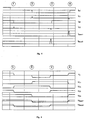
- Fig. 3 shows the voltages across the relief capacitances v C1 to v C4 , and thus the voltages across the main switches S 1 to S 4 , the converter output voltage v 0 and the voltage across the auxiliary switches S aux1 and S aux2 for an ARCP three-point converter with potential-variable intermediate circuit capacitances 1.
- a positive load current i 0 a full switching sequence from the maximum positive output voltage v 0 through the maximum negative output voltage v 0 and back is shown.
- the first two commutations 1 ⁇ 2 ⁇ are capacitive commutations.
- the output voltage v 0 is swung back to the maximum positive output voltage by means of two ARCP commutations 3 ⁇ 4 ⁇ .
- the scale of a division of the ordinate corresponds to the size of the DC voltage V dc in the DC link.
- the commutation times depend heavily on the selected circuit parameters. All courses are described in detail below.
- FIG. 4 shows the logic states of all switches in a converter phase of the ARCP Corresponding three-point converter with potential-variable intermediate circuit capacities to the commutations shown in Fig. 3.
- the auxiliary switches are only during of commutations switched on and influence the stationary operation of the Power converter not.
- FIG. 6 corresponds to FIG. 3, but shows qualitatively the course of the voltage over the relief capacitors and the potential variable DC link capacities for one Switching sequence with ARCP-supported capacitive commutation for an ARCP three-point converter with potential-variable DC link capacities.
- the ordinate division corresponds to the division in Fig. 3.
- the first two commutations 5 ⁇ 6 ⁇ are in this Case ARCP supported capacitive commutation.
- the capacitors are not linear as in Fig. 3, but reloaded with the help of a resonant vibration.
- the the following two ARCP commutations correspond qualitatively to the ARCP commutations 3 ⁇ 4 ⁇ in Fig. 3. Both the commutation times and the amount of resonant current for the ARCP supported capacitive commutations heavily dependent on the selected circuit parameters.
- FIG. 8 qualitatively shows the course of the currents introduced in FIG. 5 for the commutations discussed for FIG. 6.
- the ordinate scale in this representation corresponds to 50% of that in FIG. 5 and the load current i 0 corresponds to only 10% of the load current in the representation according to FIG. 5.
- the desired current increases in the main switches at the start of the ARCP-supported capacitive commutation are clearly visible. All current curves shown are described below.
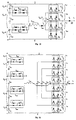
- FIG. 9 shows an alternative embodiment of an ARCP converter phase with potential-variable intermediate circuit capacitances.
- L aux is coupled to the converter output and is electrically connected in series with a bidirectional auxiliary switch S aux1 or S aux2 , which in turn are coupled to the midpoints of the potential- variable capacitances or to the midpoint 0 of the DC link capacitance.
- the reverse voltage load for the bidirectional auxiliary switches in a converter phase is therefore not the same.
- the maximum load occurs at the bidirectional auxiliary switch with connection point 0 and is V dc / 2.
- This embodiment can be extended to ARCP multi-point converters with more than 3 points by adding further auxiliary switches which connect the centers of further potential-variable intermediate circuit capacitances with the resonance inductance.
- the commutations p ⁇ 0 and 0 ⁇ n are capacitive commutations or ARCP-supported capacitive commutations in the case and the commutations n ⁇ 0 and 0 ⁇ p are ARCP commutations.
- the ARCP auxiliary branch can be used to accelerate the commutation, which leads to an ARCP-supported capacitive commutation.
- the switches S 1 and S 2 are closed before the commutation begins.
- the load current i 0 flows through the switches T 1 and T 2 .
- the inverse diodes D 3 and D 4 are in the blocking state.
- the auxiliary switches S aux1 and S aux2 are not activated for this commutation.
- ARCP commutation see image marking 4 ⁇ :
- the main switches S 2 and S 4 are closed before commutation begins.
- the load current i o flows through the power semiconductor T 2 and the inverse diode D 4 .
- the inverse diodes D 1 and D 3 are thus in the blocking state.
- the commutation is started by actively switching off the power semiconductor T 4 .
- the minimum boost current I boost is again determined by the swinging condition of v C1 ⁇ 0. Since the main switch S 2 is switched on and the voltage across the potential-variable capacitance, consisting of the series connection of C DC3 and C DC4 , is relatively constant, the difference between the load current i o and the current i aux1 commutates into the capacitors C 1 and C 4 , which leads to a charging of the capacitor C 4 and a discharge of the capacitor C 1 . In this short commutation time, the load current is led to center 0 of the converter via T 2 , C DC3 and S aux1 .
- the at ARCP multi-point converter with potential-variable intermediate circuit in the ARCP Influence potential variable DC link capacitances on the commutation circuit ARCP commutation is not as long as its capacitance value is in the order of magnitude lies above the capacity value of the relief capacities of the main switches.
Abstract
Description
Die Erfindung bezieht sich auf einen ARCP (Auxiliary Resonant Commutated Pole) Mehrpunktstromrichter mit potentialvariablen Zwischenkreiskapazitäten und damit auf Schaltungen der Leistungselektronik, insbesondere weich schaltende Mehrpunktstromrichtertopologien für Hochleistungsstromrichter.The invention relates to an ARCP (Auxiliary Resonant Commutated Pole) Multi-point converter with potential-variable DC link capacities and thus on Power electronics circuits, especially soft-switching multi-point converter topologies for high-performance converters.
Hart schaltende Mehrpunktstromrichter mit potentialveränderlichen Zwischenkreiskapazitäten, wie sie z.B. von T. Meynard et al. in dem Patent WO9302501 vorgeschlagen wurden, werden im Hochleistungsbereich zur Steuerung von Drehstromantrieben bzw. bei Energieübertragungsanlagen zur Netzkopplung und Kompensation eingesetzt. Das Mehrpunktstromrichterkonzept hat sich insbesondere bei hohen Spannungsebenen bewährt, bei denen die maximale Sperrspannung eines heute verfügbaren einzelnen Halbleiterventiles nicht ausreicht. Im Gegensatz zu den Mehrpunktstromrichtertopologien mit Null- oder Begrenzerdioden, wie sie zum Beispiel von A. Nabae et al. in "A New Neutral Point Clamped PWM Inverter", IEEE Transactions of Industry Applications, Vol-IA-17, No. 5 beschrieben wurden, werden in der von Meynard et al. vorgeschlagenen Mehrpunktstromrichtertopologie die verschiedenen Ausgangsspannungsniveaus an einem Stromrichterzweig durch geschicktes Zusammenschalten verschieden geladener Zwischenkreiskapazitäten erzielt. Die Vorteile dieser Topologie machen sich insbesondere bei Mehrpunktstromrichtern mit mehr als drei Punkten bemerkbar, bei denen die Anzahl und die erforderliche Sperrspannungsbelastung der Null- bzw. Begrenzerdioden in einer Topologie gemäß Nabae et al. stark zunimmt.Hard switching multi-point converters with variable DC link capacities, such as by T. Meynard et al. proposed in patent WO9302501 have been used in the high-performance area to control three-phase drives or used in power transmission systems for network coupling and compensation. The Multi-point converter concept has become particularly popular at high voltage levels proven, at which the maximum reverse voltage of an individual available today Semiconductor valve is not sufficient. In contrast to the multi-point converter topologies with zero or limiter diodes, as described, for example, by A. Nabae et al. in "A New Neutral Point Clamped PWM Inverter ", IEEE Transactions of Industry Applications, Vol-IA-17, No. 5 have been described in the Meynard et al. proposed Multi-point converter topology shows the different output voltage levels a converter branch by cleverly interconnecting differently charged DC link capacities achieved. The advantages of this topology are particularly apparent noticeable in multi-point converters with more than three points, where the Number and the required reverse voltage load of the zero or limiter diodes in a topology according to Nabae et al. increases rapidly.
Gegenwärtig werden in den Mehrpunktstromrichtern mit Spannungszwischenkreis im hohen Leistungsbereich GTO Schalter mit Inversdioden eingesetzt. Bei dieser Konfiguration müssen die maximal auftretenden Stromanstiege di/dt und Spannungsanstiege du/dt durch passive Begrenzernetzwerke begrenzt werden, um eine Zerstörung der Halbleiterventile zu vermeiden. Diese Netzwerke sind oft stark verlustbehaftet und tragen wesentlich zur Stromrichterkomplexität und zu den Stromrichterkosten bei.Currently, multi-point converters with a voltage intermediate circuit in the high power range GTO switches with inverse diodes are used. With this configuration the maximum current increases di / dt and voltage increases du / dt be limited by passive limiter networks to destroy the Avoid semiconductor valves. These networks are often very lossy and bear contribute significantly to converter complexity and converter costs.
Die maximal erreichbare Schaftfrequenz in diesen Hochleistungsstromrichtern ist begrenzt durch die im Halbleiter auftretenden Schaltverluste und die minimalen Schaft- und Erholzeiten der Halbleiterbauelemente. Da die Schaltfrequenz direkten Einfluß auf die Qualität der elektrischen Eingangs- und Ausgangsgrößen und somit auf das gesamte Systemdesign hat, ist die erreichbare Schaltfrequenz ein wesentliches Gütekriterium für einen Stromrichter.The maximum shaft frequency that can be achieved in these high-performance converters is limited due to the switching losses occurring in the semiconductor and the minimal shaft and Recovery times of the semiconductor components. Because the switching frequency has a direct impact the quality of the electrical input and output variables and thus of the whole System design, the achievable switching frequency is an essential quality criterion for a power converter.
Fortschritte in der Leistungshalbleiterentwicklung ermöglichen heute einen Stromrichterbetrieb mit wesentlich höherem di/dt und du/dt, was eine beträchtliche Verkleinerung oder sogar den Verzicht auf die Begrenzernetzwerke zur Folge hat. Die gegenwärtige Grenze in der erreichbaren Schaltfrequenz ist somit im wesentlichen nur noch durch die maximal zulässigen Halbleiterverluste gegeben.Advances in power semiconductor development enable converter operation today with much higher di / dt and du / dt, which is a considerable reduction or even renouncing the limiter networks. The current one The limit in the achievable switching frequency is therefore essentially only that maximum permissible semiconductor losses.
Zur Erhöhung der maximalen Schaltfrequenz in Stromrichtern im kleinen und mittleren Leistungsbereich wurden verschiedene weich schaltende Stromrichtertopologien vorgestellt, die eine wesentliche Reduktion der Schaltverluste ermöglichen. Insbesondere das im Patent US5047913 von R. De Doncker et al. vorgeschlagene "Auxiliary Resonant Commutated Pole" (ARCP) Prinzip für Zweipunktstromrichter eignet sich sehr gut zur Reduzierung von Schaltverlusten. Bei einem solchen ARCP Stromrichter ist jedem Hauptschalter ein Entlastungskondensator elektrisch parallel geschaltet. Außerdem ist eine Hilfsschaltung, bestehend aus einem Hilfsschalter, der elektrisch in Reihe mit einer Resonanz-Induktivität geschaltet ist, vorgesehen, die einen Mittelpunkt eines Gleichspannungs-Zwischenkreiskondensators mit dem Ausgangsanschluß der Stromrichterphase verbindet. Alle Hauptschalter arbeiten im Nullspannungsbetrieb, während alle Hilfsschalter im Nullstrombetrieb arbeiten.To increase the maximum switching frequency in small and medium-sized converters Different soft switching converter topologies were presented, which allow a significant reduction in switching losses. In particular that disclosed in R. De Doncker et al. US5047913. proposed "Auxiliary Resonant Commutated Pole "(ARCP) principle for two-point converters is very suitable to reduce switching losses. With such an ARCP converter everyone is Main switch a relief capacitor electrically connected in parallel. Besides, is an auxiliary circuit consisting of an auxiliary switch that is electrically in series with a Resonance inductance is connected, which is a center point of a DC link capacitor with the output connection of the converter phase connects. All main switches operate in zero voltage while all Auxiliary switches work in zero current operation.
Neben der drastischen Reduzierung der Schaltverluste ermöglicht das ARCP Prinzip auch eine Steuerung der maximalen Strom- bzw. Spannungsanstiegs-Geschwindigkeit über die Wahl der resonanten Elemente, was neben der Möglichkeit des Einsatzes kritischer Halbleiterschalter bzw. Kombinationen von Halbleiterschaltern (z. B. Serienschaltung) auch eine Reduzierung der Beanspruchung der Isolation der Endwindungen in Drehstrommotoren mit sich bringt.In addition to the drastic reduction in switching losses, the ARCP principle enables also a control of the maximum current or voltage rise speed about the choice of resonant elements, which is critical in addition to the possibility of use Semiconductor switches or combinations of semiconductor switches (e.g. series connection) also a reduction in the stress on the insulation of the end turns in three-phase motors.
Ansätze der Erweiterung dieses ARCP Prinzips auf Dreipunktstromrichter mit potentialvariablen Kapazitäten wurden von Dijkhuizen et al. auf der IEEE Konferenz IAS 98 und von Deschamps et al. bzw. von Yuan et al. auf der brasilianischen Leistungselektronik-Konferenz COBEP 97 gezeigt. In diesen Lösungen ist der Stromrichterausgang mit einer Resonanz-Induktivität verbunden, die entweder auf die positive oder die negative Gleichspannungs-Zwischenkreisschiene (Deschamps) oder über einen zusätzlichen Transformator auf den Spannungsmittelpunkt des Gleichspannungs-Zwischenkreiskondensators im Dreipunktstromrichter (Yuan) geschalten wird. Der wesentliche Nachteil in der Anordnung von Deschamps ist, daß ein unsymmetrischer Umladevorgang stattfindet, d. h. der Betrag der Spannung über der Resonanz-Induktivität am Beginn des resonanten Umladevorgangs entspricht nicht dem Betrag der Spannung zum Ende der resonanten Kommutierung. Zusätzliche verlustbehaftete Schaltvorgänge im Hilfszweig während der resonanten Kommutierung sind notwendig, um ein Abklingen des Stromes im Hilfszweig zu erreichen. Der wesentliche Nachteil in der Anordnung nach Yuan ist der hohe Bauelementeaufwand. Insbesondere die Fertigung der Hochfrequenztransformatoren im Hilfszweig, welche mit einem hohen Resonanzstrom belastet werden, ist für eine breite Anwendung dieser Topologie zu komplex und zu teuer.Approaches to extend this ARCP principle to three-point converters with potential variables Capacities were developed by Dijkhuizen et al. at the IEEE conference IAS 98 and by Deschamps et al. or by Yuan et al. at the Brazilian power electronics conference COBEP 97 shown. In these solutions, the converter output is one Resonance inductance connected to either the positive or the negative DC link rail (Deschamps) or via an additional one Transformer on the voltage center of the DC link capacitor is switched in the three-point converter (yuan). The main disadvantage in the Deschamps arrangement is that an asymmetrical transfer process takes place, d. H. the amount of voltage across the resonance inductor at the beginning the resonant charge reversal does not correspond to the amount of voltage at the end of resonant commutation. Additional lossy switching operations in the auxiliary branch during resonant commutation are necessary to decay the To reach current in the auxiliary branch. The main disadvantage in the arrangement according to Yuan is the high component cost. In particular the manufacture of high-frequency transformers in the auxiliary branch, which is loaded with a high resonance current is too complex and too expensive for a wide application of this topology.
Der Erfindung liegt die Aufgabe zugrunde, einen ARCP Mehrpunktstromrichter mit potientialvariablen Kapazitäten anzugeben, der aufgrund der Anordnung weniger zusätzlicher Schaltelemente einen symmetrischen resonanten Umladevorgang ermöglicht, um somit einen Nullstrombetrieb der Hilfsschalter und einen Nullspannungsbetrieb der Hauptschalter ohne verlustbehaftete Schaltvorgänge bzw. ohne transformatorische Übertrager zu erzielen.The invention is based, an ARCP multi-point converter with potential variables the task Capacities to indicate the additional arrangement less Switching elements enables a symmetrical resonant recharging process to thus a zero current operation of the auxiliary switches and a zero voltage operation of the Main switch without lossy switching operations or without transformer To achieve transformers.
Die Aufgabe wird gemäß einer ersten Ausführungsform erfindungsgemäß gelöst durch einen ARCP Dreipunkt- oder Mehrpunktstromrichter
- mit einer Reihenschaltung von mindestens vier Hauptschaltern pro Stromrichterphase, welche elektrisch parallel zwischen einer positiven und einer negativen Gleichspannungsschiene geschalten sind,
- wobei elektrisch parallel zu jedem einzelnen Hauptschalter eine einzelne Entlastungskapazität geschalten ist,
- wobei zwischen den Gleichspannungsschienen zwei gleich große Zwischenkreiskapazitäten angeordnet sind, deren Spannungsmittelpunkt verfügbar ist,
- wobei die Verbindungspunkte jeweils benachbarter Hauptschalter, welche nicht gleichzeitig den Ausgang der Stromrichterphase bilden, über potentialvariable Zwischenkreiskapazitäten zur Bildung von Kommutierungszellen in hinsichtlich der positiven und negativen Gleichspannungsschiene symmetrischer Weise miteinander verbunden sind,
- wobei jede potentialvariable Zwischenkreiskapazität in zwei gleich große Teilkapazitäten aufgeteilt ist, deren Verbindungpunkte als Spannungsmittelpunkte verfügbar sind,
- wobei der Ausgang der Stromrichterphase mit einer Resonanz-Induktivität verbunden ist, deren weiterer Anschluß jeweils über einen eigenen unabhängig steuerbaren bidirektionalen Hilfsschalter mit allen Spannungsmittelpunkten verbunden ist.
- with a series connection of at least four main switches per converter phase, which are electrically connected in parallel between a positive and a negative DC voltage rail,
- wherein a single relief capacity is electrically connected in parallel to each individual main switch,
- where two DC link capacitors of equal size are arranged between the DC voltage rails, the voltage center of which is available,
- the connection points of adjacent main switches, which do not simultaneously form the output of the converter phase, are connected to one another via potential-variable intermediate circuit capacitances to form commutation cells in a symmetrical manner with regard to the positive and negative DC voltage rails,
- each potential variable intermediate circuit capacitance is divided into two equal capacitances, the connection points of which are available as voltage centers,
- the output of the converter phase being connected to a resonance inductor, the further connection of which is connected to all voltage centers via a separate, independently controllable, bidirectional auxiliary switch.
Die Aufgabe wird gemäß einer zweiten Ausführungsform erfindungsgemäß gelöst durch einen ARCP Mehrpunktstromrichter
- mit einer Reihenschaltung von mehr als vier Hauptschaltern pro Stromrichterphase, welche elektrisch parallel zwischen einer positiven und einer negativen Gleichspannungsschiene geschalten sind,
- wobei elektrisch parallel zu jedem einzelnen Hauptschalter eine einzelne Entlastungskapazität geschalten ist,
- wobei zwischen den Gleichspannungsschienen zwei gleich große Zwischenkreiskapazitäten angeordnet sind, deren Spannungsmittelpunkt verfügbar ist,
- wobei die Verbindungspunkte jeweils benachbarter Hauptschalter, welche nicht gleichzeitig den Ausgang der Stromrichterphase bilden, über potentialvariable Zwischenkreiskapazitäten zur Bildung von Kommutierungszellen in hinsichtlich der positiven und negativen Gleichspannungsschiene symmetrischer Weise miteinander verbunden sind,
- wobei jede potentialvariable Zwischenkreiskapazität in zwei gleich große Teilkapazitäten aufgeteilt ist, deren Verbindungpunkte als Spannungsmittelpunkte verfügbar sind,
- wobei der Spannungsmittelpunkt der Zwischenkreiskapazitäten über einen unabhängig steuerbaren bidirektionalen Hilfsschalter und eine Resonanz-Induktivität mit dem Spannungsmittelpunkt der nächstliegenden Kommutierungszelle verbunden ist, der Ausgang der Stromrichterphase über einen unabhängig steuerbaren bidirektionalen Hilfsschalter und eine Resonanz-Induktivität mit dem Spannungsmittelpunkt der nächstliegenden Kommutierungszelle verbunden ist und die Spannungsmittelpunkte jeweils benachbarter Kommutierungszellen über einen unabhängig steuerbaren bidirektionalen Hilfsschalter und eine Resonanz-Induktivität miteinander verbunden sind.
- with a series connection of more than four main switches per converter phase, which are electrically connected in parallel between a positive and a negative DC voltage rail,
- wherein a single relief capacity is electrically connected in parallel to each individual main switch,
- where two DC link capacitors of equal size are arranged between the DC voltage rails, the voltage center of which is available,
- the connection points of adjacent main switches, which do not simultaneously form the output of the converter phase, are connected to one another via potential-variable intermediate circuit capacitances to form commutation cells in a symmetrical manner with regard to the positive and negative DC voltage rails,
- each potential variable intermediate circuit capacitance is divided into two equal capacitances, the connection points of which are available as voltage centers,
- wherein the voltage center of the intermediate circuit capacitances is connected to the voltage center of the nearest commutation cell via an independently controllable bidirectional auxiliary switch and a resonance inductor, the output of the converter phase is connected to the voltage center of the nearest commutation cell via a independently controllable bidirectional auxiliary switch and a resonance inductor, and that Voltage centers of adjacent commutation cells are connected to one another via an independently controllable bidirectional auxiliary switch and a resonance inductor.
Die Aufgabe wird gemäß einer dritten Ausführungsform erfindungsgemäß gelöst durch einen ARCP Dreipunkt- oder Mehrpunktstromrichter
- mit einer Reihenschaltung von mindestens vier Hauptschaltern pro Stromrichterphase, welche elektrisch parallel zwischen einer positiven und einer negativen Gleichspannungsschiene geschalten sind,
- wobei elektrisch parallel zu jedem einzelnen Hauptschalter eine einzelne Entlastungskapazität geschalten ist,
- wobei zwischen den Gleichspannungsschienen mindestens drei Zwischenkreiskapazitäten angeordnet sind, deren Kapazitätswerte derart gewählt sind, daß Spannungsabgriffe entstehen, deren Spannungsniveaus in der Mitte der am Ausgang der Stromrichterphase einstellbaren Spannungsniveaus liegen,
- wobei die Verbindungspunkte jeweils benachbarter Hauptschalter, welche nicht gleichzeitig den Ausgang der Stromrichterphase bilden, über potentialvariable Zwischenkreiskapazitäten zur Bildung von Kommutierungszellen in hinsichtlich der positiven und negativen Gleichspannungsschiene symmetrischer Weise miteinander verbunden sind,
- wobei der Ausgang der Stromrichterphase mit einer Resonanz-Induktivität verbunden ist, deren weiterer Anschluß jeweils über einen eigenen unabhängig steuerbaren bidirektionalen Hilfsschalter mit allen Spannungsabgriffen verbunden ist.
- with a series connection of at least four main switches per converter phase, which are electrically connected in parallel between a positive and a negative DC voltage rail,
- wherein a single relief capacity is electrically connected in parallel to each individual main switch,
- wherein at least three intermediate circuit capacitances are arranged between the DC voltage rails, the capacitance values of which are selected in such a way that voltage taps are produced, the voltage levels of which lie in the middle of the voltage levels which can be set at the output of the converter phase,
- the connection points of adjacent main switches, which do not simultaneously form the output of the converter phase, are connected to one another via potential-variable intermediate circuit capacitances to form commutation cells in a symmetrical manner with regard to the positive and negative DC voltage rails,
- the output of the converter phase being connected to a resonance inductor, the further connection of which is connected to all voltage taps via its own independently controllable bidirectional auxiliary switch.
Durch die Anordnung mehrerer Stromrichterphasen,
- die jeweils elektrisch parallel zu einem mit einem Kondensator abgestützten Gleichspannungs-Zwischenkreis geschaltet sind,
- jeweils 2(n-1) in Serie geschaltete aktive Hauptschalter aufweisen (n = Anzahl der Stromrichterpunkte bzw. Anzahl der möglichen Ausgangsspannungsniveaus), die den positiven mit den negativen Anschluß der Gleichspannungs-Zwischenkreiskapazität verbinden,
- jeweils einen Ausgangsanschluß für die Stromrichterphase an dem Verbindungspunkt des (n-1)-ten und des n-ten Hauptschalters verzeichnen,
- jeweils (n-2) potentialvariable Zwischenkreiskapazitäten besitzen, deren positive Anschlußpunkte
in der Kette der in Serie geschalteten Hauptschalter am Verbindungspunkt
zwischen den Schaltern (n-1-k) und (n-2-k) und deren negative Anschlußpunkte
am Verbindungspunkt der Hauptschalter (n+k) und (n+1+k) mit k=0 ... (n-3) angeschlossen
werden,
erhält man den Aufbau eines mehrphasigen Mehrpunktstromrichters mit potentialvariablen Zwischenkreiskapazitäten.
- which are each electrically connected in parallel to a DC intermediate circuit supported by a capacitor,
- each have 2 (n-1) active main switches connected in series (n = number of converter points or number of possible output voltage levels), which connect the positive with the negative connection of the DC link capacitance,
- each have an output connection for the converter phase at the connection point of the (n-1) th and the n-th main switch,
- each have (n-2) potential-variable intermediate circuit capacitances, the positive connection points of which in the chain of main switches connected in series at the connection point between switches (n-1-k) and (n-2-k), and the negative connection points of which at the connection point of main switches ( n + k) and (n + 1 + k) with k = 0 ... (n-3),
you get the construction of a multi-phase multi-point converter with potential variable DC link capacities.
Ausgehend von dieser hart schaltenden Mehrpunktstromrichtertopologie mit potentialvariablen
Zwischenkreiskapazitäten wird die gewünschte weich schaltende ARCP
Mehrpunktstromrichtertopologie mit potentialvariablen Zwischenkreiskapazitäten durch
folgende Modifikationen und Erweiterungen erzielt:
Somit erhält man vorteilhaft einen verlustarmen ARCP Mehrpunktstromrichter, der die Vorteile eines Mehrpunktstromrichters mit potentialvariablen Zwischenkreiskapazitäten mit denen eines ARCP-Stromrichters kombiniert, wobei eine maximale Schaltentlastung erzielt werden kann.This results in a low-loss ARCP multi-point converter, which Advantages of a multi-point converter with variable DC link capacities combined with those of an ARCP converter, with a maximum switching relief can be achieved.
Mit dieser Topologie ist es möglich, den Schaltaugenblick der Hauptschalter der Stromrichterphase
frei festzulegen, wodurch herkömmliche Pulsweitenmodulationsverfahren
eingesetzt werden können. Die Hauptschalter in dieser ARCP Stromrichterphase
schalten bei verschwindender Spannung über diesen Bauelementen ein und aus (Zero-Voltage-Switch-(ZVS)-Prinzip).
Die Hilfsschalter in Reihe zur Resonanz-Induktivität
werden nach dem Zero-Current-Switch-(ZCS-) Prinzip ebenfalls schaltentlastend betrieben.
Beim ZCS-Prinzip wird der Hilfsschalter bei verschwindendem Strom ein- und
abgeschaltet. Das heißt, alle in dieser Stromrichterphase verwendeten Halbleiterschalter
schalten verlustarm. Die spannungsmäßige Auslegung der Hauptschalter und Hilfsschalter
sowie die Betriebsweise der Schalter kann der nachstehenden Tabelle 1 entnommen
werden. Die Auslegung der Schalter bzgl. des Nennstromes hängt von den
Schaltungsparametern, die den Effektivstrom durch den Schalter bestimmen, und den
thermischen und elektrischen Eigenschaften der Schalter ab. Die Vorteile dieser ARCP
Mehrpunktstromrichtertopologie mit potentialvariablen Zwischenkreiskapazitäten gegenüber
den bisher vorgestellten ARCP Dreipunktstromrichtern sind:
Zur weiteren Erläuterung der Erfindung wird auf die Zeichnungen Bezug genommen, in denen Ausführungsbeispiele einer Stromrichterphase eines verlustarmen ARCP Mehrpunktstromrichters mit potentialvariablen Zwischenkreiskapazitäten schematisch veranschaulicht sind. Es zeigen:
- Fig. 1
- eine Ausgangsphase eines ARCP Dreipunktstromrichters mit potentialvariablen Zwischenkreiskapazitäten,
- Fig. 2
- eine Phase eines ARCP Fünfpunktstromrichters mit potentialvariablen Zwischenkreiskapazitäten, welcher nach den benannten Designrichtlinien entworfen wurde,
- Fig. 3
- qualitativ den Verlauf der Spannung über den Entlastungskapazitäten C1 bis C4, die Spannung über den Hilfsschaltern Saux1 und Saux2, sowie die Ausgangsspannung v0 für einen ARCP Dreipunktstromrichter mit potentialvariablen Zwischenkreiskapazitäten und positivem Ausgangsstrom io,
- Fig. 4
- die Schaltzustände für die steuerbaren Schalter innerhalb einer Schaltsequenz für einen ARCP Dreipunktstromrichter mit potentialvariablen Zwischenkreiskapazitäten und positivem Ausgangsstrom io,
- Fig. 5
- qualitativ den Verlauf der Ströme durch die Hilfsschalter Saux1 und Saux2, durch die Hauptschalter S1 und S2 sowie durch die Entlastungskapazitäten C1 und C2 für einen ARCP Dreipunktstromrichter,
- Fig. 6, 7, 8
- Zusammenhänge entsprechend den Fig. 3, 4
und 5, jedoch für ARCP unterstützte kapazitive Kommutierungen für einen ARCP Dreipunktstromrichter mit potentialvariablen Zwischenkreiskapazitäten, - Fig. 9, 10, 11
- alternative Ausführungsformen einer ARCP Stromrichterphase mit potentialvariablen Zwischenkreiskapazitäten.
- Fig. 1
- an output phase of an ARCP three-point converter with potential-variable intermediate circuit capacities,
- Fig. 2
- one phase of an ARCP five-point converter with potential-variable intermediate circuit capacities, which was designed according to the named design guidelines,
- Fig. 3
- qualitatively the course of the voltage across the relief capacitances C 1 to C 4 , the voltage across the auxiliary switches S aux1 and S aux2 , and the output voltage v 0 for an ARCP three-point converter with potential-variable intermediate circuit capacitances and positive output current i o ,
- Fig. 4
- the switching states for the controllable switches within a switching sequence for an ARCP three-point converter with potential-variable intermediate circuit capacitances and positive output current i o ,
- Fig. 5
- qualitatively the course of the currents through the auxiliary switches S aux1 and S aux2 , through the main switches S 1 and S 2 and through the relief capacitances C 1 and C 2 for an ARCP three-point converter,
- 6, 7, 8
- Relationships according to FIGS. 3, 4 and 5, but for ARCP supported capacitive commutations for an ARCP three-point converter with potential-variable intermediate circuit capacitances,
- 9, 10, 11
- alternative embodiments of an ARCP converter phase with potential-variable intermediate circuit capacities.
Fig. 1 zeigt den Aufbau einer Ausgangsphase eines Dreipunktstromrichters, bestehend
aus einer Reihenschaltung der Hauptschalter S1 bis S4, die elektrisch parallel zu einem
Gleichspannungszwischenkreis geschaltet sind, welcher aus einer Reihenschaltung der
gleich großen Kapazitäten CDC1 und CDC2 besteht und damit die positive Gleichspannungsschiene
2 mit der negativen Gleichspannungsschiene 4 verbindet. Fig. 1 shows the structure of an output phase of a three-point converter, consisting of a series circuit of the main switches S 1 to S 4 , which are electrically connected in parallel to a DC voltage intermediate circuit, which consists of a series circuit of the same capacitance C DC1 and C DC2 and thus the
Direkt parallel zu jedem Hauptschalter S1 bis S4 sind die Entlastungskapazitäten C1 bis C4 geschaltet. Die Schalter S1 bis S4 bestehen jeweils aus einem aktiv ausschaltbaren Leistungshalbleiter T1 ...T4, allgemein T mit antiparallel geschalteter Diode D1... D4, allgemein D (Inversdiode). An den Verbindungspunkten 7 bzw. 9 der Hauptschalter S1 und S2 bzw. der Hauptschalter S3 und S4 ist die potentialvariable Zwischenkreiskapazität, bestehend aus den Teilkapazitäten CDC3 bis CDC4, geschaltet.The relief capacitances C 1 to C 4 are connected directly in parallel to each main switch S 1 to S 4 . The switches S 1 to S 4 each consist of an actively switchable power semiconductor T 1 ... T 4 , generally T with an anti-parallel diode D 1 ... D 4 , generally D (inverse diode). The potential-variable intermediate circuit capacitance, consisting of the partial capacitances C DC3 to C DC4 , is connected at the connection points 7 and 9 of the main switches S 1 and S 2 or the main switches S 3 and S 4 .
Die Spannungsmittelpunkte 0 bzw. 1 des Gleichspannungs-Zwischenkreiskondensators
bzw. der potentialvariablen Zwischenkreiskapazität sowie der Spannungsmittelpunkt 1
und der Ausgang 10 der Stromrichterphase sind jeweils mittels einer Serienschaltung
bestehend aus einer Resonanz-Induktivität und eines Hilfsschalters verbunden. Die
Hilfsschalter bestehen aus einer Serienschaltung von zwei aktiv ausschaltbaren Leistungshalbleitern
mit antiparallelen Dioden, die so miteinander verschaltet sind, daß ein
bidirektionaler Schalter entsteht.The
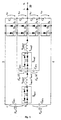
Fig. 2 zeigt eine Erweiterung der Ausführungsform in Fig. 1 auf einen ARCP Fünfpunktstromrichter.FIG. 2 shows an extension of the embodiment in FIG. 1 to an ARCP five-point converter.
Die Ausgangsphase des Fünfpunktstromrichters besteht aus einer Reihenschaltung der
Hauptschalter S1 bis S8, die elektrisch parallel zu einem Gleichspannungszwischenkreis
geschaltet sind, welcher aus einer Reihenschaltung von zwei gleich großen Kapazitäten
CDC1 bis CDC2 besteht und damit die positive Gleichspannungsschiene 2 mit der negativen
Gleichspannungsschiene 4 verbindet.The output phase of the five-point converter consists of a series connection of the main switches S 1 to S 8 , which are electrically connected in parallel to a DC voltage intermediate circuit, which consists of a series connection of two capacitors C DC1 to C DC2 of the same size and thus the
Die Schalter S1 bis S8 bestehen jeweils aus einem aktiv ausschaftbaren Leistungshalbleiter T mit antiparallel geschalteter Diode D. Die Verbindungspunkte 27 bzw. 49 der Hauptschalter S1 und S2 bzw. der Hauptschalter S7 und S8 sind mit einer potentialvariablen Kapazität verbunden, die aus den Teilkapazitäten CDC3 und CDC4 gebildet wird. Die Verbindungspunkte 7 bzw. 9 der Hauptschalter S2 und S3 bzw. der Hauptschalter S6 und S7 sind mit einer potentialvariablen Kapazität verbunden, die aus den Teilkapazitäten CDC5 und CDC6 gebildet wird. Weiterhin sind die Verbindungspunkte 17 bzw. 19 der Hauptschalter S3 und S4 bzw. der Hauptschalter S5 und S6 mit einer potentialvariablen Kapazität verbunden, die aus den Teilkapazitäten CDC7 und CDC8 gebildet wird.The switches S 1 to S 8 each consist of an active ausschaftbaren power semiconductor T with anti-parallel diode D. The connection points 27 and 49 of the main switch S 1 and S 2 and the main switch S 7 and S 8 are connected to a potential variable capacitance, which is formed from the partial capacitances C DC3 and C DC4 . The connection points 7 and 9 of the main switches S 2 and S 3 and the main switches S 6 and S 7 are connected to a potential- variable capacitance which is formed from the partial capacitances C DC5 and C DC6 . Furthermore, the connection points 17 and 19 of the main switches S 3 and S 4 and the main switches S 5 and S 6 are connected to a potential- variable capacitance which is formed from the partial capacitances C DC7 and C DC8 .
Die Entlastungskapazitäten C1 bis C8 sind direkt parallel zu den Hauptschaltern S1 bis S8 geschaltet. Zusätzlich sind die Spannungsmittelpunkte 0, 1, 3 und 5 an den potentialvariablen Zwischenkreiskapazitäten sowie der Ausgang der Stromrichterphase jeweils über eine Serienschaltung aus einem bidirektionalen Hilfsschalter und einer Resonanz-Induktivität Laux verbunden. Die Hilfsschalter bestehen aus einer Serienschaltung von zwei aktiv ausschaltbaren Leistungshalbleitern mit antiparallelen Dioden, die so miteinander verschalten sind, daß ein bidirektionaler Schalter entsteht.The relief capacitances C 1 to C 8 are connected directly in parallel to the main switches S 1 to S 8 . In addition, the voltage centers 0, 1, 3 and 5 at the potential-variable intermediate circuit capacitances and the output of the converter phase are each connected via a series circuit comprising a bidirectional auxiliary switch and a resonance inductor L aux . The auxiliary switches consist of a series connection of two power semiconductors that can be actively switched off, with anti-parallel diodes, which are interconnected so that a bidirectional switch is created.
Fig. 3 stellt die Spannungen über den Entlastungskapazitäten vC1 bis vC4, und damit die
Spannungen über den Hauptschaltern S1 bis S4, die Stromrichterausgangsspannung v0
und die Spannung über den Hilfsschaltern Saux1 und Saux2 für einen ARCP Dreipunktstromrichter
mit potentialvariablen Zwischenkreiskapazitäten gemäß Fig. 1 dar. Unter
Annahme eines positiven Laststromes i0 ist eine volle Schaltsequenz von der maximalen
positiven Ausgangsspannung v0 über die maximale negative Ausgangsspannung v0
und zurück dargestellt. Die ersten beiden Kommutierungen 1 ○ 2 ○ sind kapazitive Kommutierungen.
Die Ausgangsspannung v0 wird mittels zweier ARCP Kommutierungen
3 ○ 4 ○ wieder auf die maximale positive Ausgangsspannung zurückgeschwungen. Der
Maßstab einer Teilung der Ordinate entspricht der Größe der Gleichspannung Vdc im
Gleichspannungszwischenkreis. Die Kommutierungszeiten sind stark von den gewählten
Schaltungsparametern abhängig. Alle Verläufe werden im weiteren im Detail beschrieben.Fig. 3 shows the voltages across the relief capacitances v C1 to v C4 , and thus the voltages across the main switches S 1 to S 4 , the converter output voltage v 0 and the voltage across the auxiliary switches S aux1 and S aux2 for an ARCP three-point converter with potential-variable
Fig. 4 zeigt die Logikzustände aller Schalter in einer Stromrichterphase des ARCP Dreipunktstromrichters mit potentialvariablen Zwischenkreiskapazitäten korrespondierend zu den in Fig. 3 dargestellten Kommutierungen. Die Hilfsschalter sind nur während der Kommutierungen eingeschaltet und beeinflussen den stationären Betrieb des Stromrichters nicht. 4 shows the logic states of all switches in a converter phase of the ARCP Corresponding three-point converter with potential-variable intermediate circuit capacities to the commutations shown in Fig. 3. The auxiliary switches are only during of commutations switched on and influence the stationary operation of the Power converter not.
Fig. 5 gibt qualitativ die Stromverläufe durch die Hilfsschalter Saux1 und Saux2 wieder. Weiterhin sind die Ströme in den Hauptschaltern S1 und S2 sowie den Entlastungskapazitäten C1 und C2 dargestellt. Die Höhe des resonanten Stromes ist durch die Wahl der resonanten Elemente und durch die Höhe des Booststromes beeinflußbar. Eine Ordinatenteilung entspricht der Größe des Ausgangsstrom io. Der Kommutierungsablauf korrespondiert zu den Beschreibungen für Fig. 3 und Fig. 4.5 qualitatively shows the current profiles through the auxiliary switches S aux1 and S aux2 . The currents in the main switches S 1 and S 2 and the relief capacitances C 1 and C 2 are also shown. The level of the resonant current can be influenced by the choice of the resonant elements and by the level of the boost current. Ordinate division corresponds to the size of the output current i o . The commutation process corresponds to the descriptions for FIGS. 3 and 4.
Fig. 6 entspricht Fig. 3, zeigt jedoch qualitativ den Verlauf der Spannung über den Entlastungskapazitäten
und den potentialvariablen Zwischenkreiskapazitäten für eine
Schaltsequenz mit ARCP unterstützter kapazitiver Kommutierung für einen ARCP Dreipunktstromrichter
mit potentialvariablen Zwischenkreiskapazitäten. Die Ordinatenteilung
entspricht der Teilung in Fig. 3. Die ersten beiden Kommutierungen 5 ○ 6 ○ sind in diesem
Fall ARCP unterstützte kapazitive Kommutierungen. Die Kondensatoren werden nicht
linear wie in Fig. 3, sondern mit Hilfe einer resonanten Schwingung umgeladen. Die
darauffolgenden zwei ARCP Kommutierungen entsprechen qualitativ den ARCP Kommutierungen
3 ○ 4 ○ im Fig. 3. Sowohl die Kommutierungszeiten als auch die Höhe des
resonanten Stromes für die ARCP unterstützten kapazitiven Kommutierungen sind
stark von den gewählten Schaltungsparametern abhängig.FIG. 6 corresponds to FIG. 3, but shows qualitatively the course of the voltage over the relief capacitors
and the potential variable DC link capacities for one
Switching sequence with ARCP-supported capacitive commutation for an ARCP three-point converter
with potential-variable DC link capacities. The ordinate division
corresponds to the division in Fig. 3. The first two
Fig. 7 entspricht Fig. 4 und zeigt die Ansteuerlogik für alle Schalter für die unter Fig. 6 diskutierten Kommutierungen. Auch hier werden die Hilfsschalter Saux1 und Saux2 nur zu den Kommutierungen aktiviert.FIG. 7 corresponds to FIG. 4 and shows the control logic for all switches for the commutations discussed under FIG. 6. Here too, the auxiliary switches S aux1 and S aux2 are only activated for commutation.
Fig. 8 zeigt qualitativ den Verlauf der in Fig. 5 eingeführten Ströme für die für Fig. 6 diskutierten Kommutierungen. Der Ordinatenmaßstab in dieser Darstellung entspricht 50% dessen in Fig. 5 und der Lasttrom i0 entspricht nur 10% des Laststromes in Darstellung gemäß Fig. 5. Deutlich sichtbar sind die gewünschten Stromüberhöhungen in den Hauptschaltern am Beginn der ARCP unterstützten kapazitiven Kommutierung. Alle dargestellten Stromverläufe sind im weiteren beschrieben.FIG. 8 qualitatively shows the course of the currents introduced in FIG. 5 for the commutations discussed for FIG. 6. The ordinate scale in this representation corresponds to 50% of that in FIG. 5 and the load current i 0 corresponds to only 10% of the load current in the representation according to FIG. 5. The desired current increases in the main switches at the start of the ARCP-supported capacitive commutation are clearly visible. All current curves shown are described below.
Fig. 9 zeigt eine alternative Ausführungsform einer ARCP Stromrichterphase mit potentialvariablen
Zwischenkreiskapazitäten. Gegenüber der Ausführungsform in Fig. 1 ist
nur eine Resonanz-Induktivität Laux vorgesehen. Diese wird am Stromrichterausgang
angekoppelt und ist jeweils mit einem bidirektionalen Hilfsschalter Saux1 bzw. Saux2, welche
ihrerseits an den Mittelpunkten der potentialvariablen Kapazitäten bzw. am Mittelpunkt
0 der Gleichspannungs-Zwischenkreiskapazität angekoppelt sind, elektrisch in
Reihe geschaltet. Die Sperrspannungsbelastung für die bidirektionalen Hilfsschalter in
einer Stromrichterphase ist somit nicht gleich. Die maximale Belastung tritt am bidirektionalen
Hilfsschalter mit Anschlußpunkt 0 auf und beträgt Vdc/2. Diese Ausführungsform
läßt sich durch Hinzufügen weiterer Hilfsschalter, welche die Mittelpunkte weiterer
potentialvariabler Zwischenkreiskapazitäten mit der Resonanz-Induktivität verbinden,
auf ARCP Mehrpunkt-Stromrichter mit mehr als 3 Punkten erweitern.9 shows an alternative embodiment of an ARCP converter phase with potential-variable intermediate circuit capacitances. Compared to the embodiment in Fig. 1, only one resonance inductor L aux is provided. This is coupled to the converter output and is electrically connected in series with a bidirectional auxiliary switch S aux1 or S aux2 , which in turn are coupled to the midpoints of the potential- variable capacitances or to the
Fig. 10 zeigt am Beispiel einer ARCP Dreipunktstromrichterphase eine weitere alternative Ausführungsform einer ARCP Stromrichterphase mit potentialvariablen Zwischenkreiskapazitäten. Gegenüber den bisher gezeigten Ausführungsformen sind die potentialvariablen Kapazitäten nicht in Teilkapazitäten aufgeteilt. Statt dessen ist die Kapazität im Gleichspannungszwischenkreis in mindestens n Teilkapazitäten untergliedert, an deren Verbindungsstellen (n-1) bidirektionale Hilfsschalter angeschlossen sind. Der zweite Anschluß dieser bidirektionalen Hilfsschalter wird gemeinsam auf eine Resonanz-Induktivität Laux geführt, die mit dem Stromrichterausgang verbunden ist. Eine maximale Sperrspannungsbelastung über den Hilfsschaltern von 3/4Vdc kennzeichnet diese Topologie.10 shows, using the example of an ARCP three-point converter phase, a further alternative embodiment of an ARCP converter phase with potential-variable intermediate circuit capacitances. Compared to the previously shown embodiments, the potential-variable capacities are not divided into partial capacities. Instead, the capacitance in the DC voltage intermediate circuit is subdivided into at least n partial capacitances, at the connection points (n-1) of which bidirectional auxiliary switches are connected. The second connection of these bidirectional auxiliary switches is led together to a resonance inductor L aux , which is connected to the converter output. This topology is characterized by a maximum reverse voltage load of 3 / 4V dc across the auxiliary switches.
Fig. 11 zeigt eine Erweiterung der Anordnung in Fig. 10 auf einen ARCP Fünfpunktstromrichter
mit potentialvariablen Zwischenkreiskapazitäten zur Verdeutlichung der
notwendigen Verhältnisse der Teilspannungen über den Teilkapazitäten im Gleichspannungszwischenkreis.
Bei der Auslegung der Kondensatoren im Gleichspannungszwischenkreis
sind für diese Topologie (n-1) Spannungsabgriffe vorzusehen, die bezüglich
des Stromrichtermittelpunkts 0 Spannungen aufweisen, welche dem arithmetischen
Mittelwert der vor und nach den Kommutierungen auftretenden Ausgangsspannungen
v0 entsprechen. Die maximal auftretende Sperrspannungsbelastung tritt bei den
Hilfsschaltern Saux1 und Saux
Im folgenden soll nun die Funktionsweise an einer Stromrichterphase gemäß Fig. 1
dieses erfindungsgemäßen, verlustarmen ARCP Mehrpunktstromrichters mit potentialvariablen
Zwischenkreiskapazitäten anhand der Kommutierungsvorgänge von den oberen
Hauptschaltern S1 und S2 auf die unteren Hauptschalter S3 und S4 sowie zurück
beschrieben werden. Für Mehrpunktstromrichter mit mehr als drei Punkten sind diese
Ausführungen sinngemäß anzuwenden. Für den Betrieb eines Dreipunktstromrichters
mit potentialvariablen Zwischenkreiskapazitäten sind die in der nachfolgenden Tabelle
2 gezeigten Schaltzustände maßgebend, um die gewünschten Ausgangsspannungen
v0 bezüglich des Stromrichtermittelpunkts 0 (siehe Spalte 2) zu erzielen. Es existieren
zwei alternative Schaltzustände, die eine Ausgangsspannung von Null erzeugen. Im
folgenden sind die Transitionen p→0+→n→0-→p beschrieben.
Eine detaillierte Beschreibung der einzelnen Schalttransitionen ist im folgenden für einen positiven Ausgangsstrom i0 gegeben. Die Kommutierungen p→0 und 0→n sind in dem Fall kapazitive Kommutierungen bzw. ARCP unterstützte kapazitive Kommutierungen und die Kommutierungen n→0 und 0→p sind ARCP Kommutierungen. Bei relativ kleinem Ausgangsstrom, relativ großen Entlastungskapazitäten bzw. relativ großer Gleichspannung kann es zu ungewollt langen Kommutierungszeiten für die kapazitive Kommutierung kommen. Um die Kommutierungsdauer für die kapazitive Kommutierung zu verkürzen, kann man den ARCP Hilfszweig zur Beschleunigung der Kommutierung nutzen, was zu einer ARCP unterstützten kapazitiven Kommutierung führt.A detailed description of the individual switching transitions is given below for a positive output current i 0 . The commutations p → 0 and 0 → n are capacitive commutations or ARCP-supported capacitive commutations in the case and the commutations n → 0 and 0 → p are ARCP commutations. With a relatively small output current, a relatively large relief capacitance or a relatively large DC voltage, undesired long commutation times for capacitive commutation can occur. To shorten the commutation period for capacitive commutation, the ARCP auxiliary branch can be used to accelerate the commutation, which leads to an ARCP-supported capacitive commutation.
Nachfolgend wird eine Kommutierung p→0 für i0>0+ behandelt: A commutation p → 0 for i 0 > 0 + is dealt with below:
Vor Beginn der Kommutierung sind die Schalter S1 und S2 geschlossen. Der Ausgangsstrom
io fließt durch die Schalter T1 und T2. Die Spannung über den Schaltern S3 und S4
ist jeweils
Die Kommutierung der Hauptschalter ist beendet, wenn die Spannung über dem Kondensator
C3 den Wert vC3=0 erreicht hat und der Schalter S3 mit der Diode D3 unter ZVS
Bedingung einschaltet. Damit ist die Kommutierung abgeschlossen und der "0+" Zustand
ist erreicht. Die Schalter S1 und S3 sind eingeschalten und die Spannungen vC2
und vC4 betragen jeweils Vdc/2. Die Hilfsschalter Saux1 und Saux2 werden für diese Kommutierung
nicht aktiviert.The switches S 1 and S 2 are closed before the commutation begins. The output current i o flows through the switches T 1 and T 2 . The voltage across the switches S 3 and S 4 is in each case
The commutation of the main switch is ended when the voltage across the capacitor C 3 has reached the value v C3 = 0 and the switch S 3 switches on with the diode D 3 under the ZVS condition. This completes the commutation and the "0 + " state has been reached. The switches S 1 and S 3 are switched on and the voltages v C2 and v C4 are each V dc / 2. The auxiliary switches S aux1 and S aux2 are not activated for this commutation.
Vor Beginn der Kommutierung sind die Schalter S1 und S2 geschlossen. Der Laststrom
i0 fließt durch die Schalter T1 und T2. Die Spannung über den Schaltern S3 und S4 ist
jeweils
Der Kommutierungsvorgang wird mit dem Einschalten von Saux2 bei iaux2=0 (ZCS) gestartet.
Wegen der nun negativen Spannung
Nach dem Ausschalten von T2 kommutiert der Umladestrom, bestehend aus einer
Überlagerung von dem Laststrom i0 und dem Strom iaux2, in die Kondensatoren C2 und
C3 und lädt diese um. Dabei wird der Kondensator C2 nichtlinear geladen, während der
Kondensator C3 dementsprechend entladen wird. Beide Hälften des Laststromes werden
über die positive Gleichspannungsschiene 2 geführt, während der resonante Anteil
nur durch die potentialvariablen Kapazitäten CDC3 und CDC
Die Kommutierung der Hauptschalter ist beendet, wenn die Spannung über C3 den
Wert vC3=0 erreicht hat und der Schalter S3 unter ZVS Bedingungen eingeschalten wird.
Eine positive Spannung von
The commutation process is started when S aux2 is switched on when i aux2 = 0 (ZCS). Because of the now negative tension
After T 2 has been switched off , the charge-reversal current, consisting of a superimposition of the load current i 0 and the current i aux2 , commutates into the capacitors C 2 and C 3 and recharges them. The capacitor C 2 is charged non-linearly, while the capacitor C 3 is discharged accordingly. Both halves of the load current are conducted via the positive
The commutation of the main switch is ended when the voltage across C 3 has reached the value v C3 = 0 and the switch S 3 is switched on under ZVS conditions. A positive tension of
Vor Beginn der Kommutierung sind die Schalter S1 und S3 geschlossen. Der Laststrom
i0 fließt durch T1 und die Inversdiode D3. Die Spannung über den Schaltern S2 und S4 ist
jeweils
Die Kommutierung wird initiiert, indem der Schalter T1 aktiv ausgeschaltet wird. Der
Laststrom i0 kommutiert jeweils zur Hälfte in die Kondensatoren C1 und C4, wobei diese
umgeladen werden. Dabei steigt die Spannung am Kondensator C1 linear an, während
die Spannung am Kondensator C4 linear fällt. Ein Umladen des Kondensators C2 wird
anforderungsgemäß durch die potentialvariable Zwischenkreiskapazität, bestehend aus
CDC3 und CDC4, und dem geschlossenen Schalter S3 verhindert, was die Spannung über
den Schaltern S2 und S3 konstant auf
Die Kommutierung ist beendet, wenn die Spannung über C4 den Wert vC4=0 erreicht hat
und der Schalter S4 unter ZVS Bedingung eingeschaltet wird. Der Laststrom io, der während
der Kommutierung jeweils zur Hälfte von der positiven Gleichspannungsschiene 2
und der negativen Gleichspannungsschiene 4 getragen wurde, kommutiert nun komplett
auf die Inversdioden D3 und D4. Damit ist die Kommutierung beendet und der "n"
Zustand mit einer Ausgangsspannung von
Commutation is initiated by actively switching off switch T 1 . Half of the load current i 0 commutates into the capacitors C 1 and C 4 , these being recharged. The voltage across capacitor C 1 increases linearly, while the voltage across capacitor C 4 falls linearly. A recharging of the capacitor C 2 is prevented as required by the potential-variable intermediate circuit capacitance, consisting of C DC3 and C DC4 , and the closed switch S 3 , which keeps the voltage across the switches S 2 and S 3 constant
Commutation is complete when the voltage across C 4 has reached the value v C4 = 0 and switch S 4 is switched on under the ZVS condition. The load current i o , which was carried in half by the positive
Vor Beginn der Kommutierung sind die Schalter S1 und S3 geschlossen. Der Laststrom
i0 fließt durch T1 und die Inversdiode D3. Die Spannung über den Schaltern S2 und S4 ist
jeweils
Die Kommutierung wird mit dem Einschalten des Hilfsschalters Saux1 bei iaux1=0 (ZCS)
gestartet. Wegen der damit verbundenen negativen Spannung
Da der Hauptschalter S3 eingeschalten bleibt und die Spannung über der potentialvariablen
Zwischenkreiskapazität relativ konstant ist, kommutiert der Laststrom i0 mit dem
überlagerten Strom iaux1 nach dem Ausschalten von T1 in die Kondensatoren C1 und C4
und lädt diese um. Dabei steigt die Spannung am Kondensator C1 nichtlinear an, während
die Spannung am Kondensator C4 entsprechend fällt. Die Spannungen über den
Kondensatoren C2 und C3 bleiben jeweils konstant bei
Die Kommutierung der Hauptschalter ist beendet, wenn die Spannung über dem Kondensator
C4 den Wert vC4=0 erreicht hat und der Schalter S4 unter ZVS Bedingungen
eingeschalten wurde. Der Umladestrom, bestehend aus Laststrom io und Strom iaux1 ,
kommutiert nun von der positiven Gleichspannungsschiene, die während der Kommutierung
die Hälfte dieses Umladestromes getragen hat, komplett auf die Inversdioden in
S3 und S4. Eine positive Spannung von
Commutation is started by switching on the auxiliary switch S aux1 at i aux1 = 0 (ZCS). Because of the associated negative tension
Since the main switch S 3 remains switched on and the voltage across the potential- variable intermediate circuit capacitance is relatively constant, the load current i 0 commutates with the superimposed current i aux1 after switching off T 1 into the capacitors C 1 and C 4 and reloads them. The voltage across capacitor C 1 rises non-linearly, while the voltage across capacitor C 4 drops accordingly. The voltages across the capacitors C 2 and C 3 remain constant
The commutation of the main switches is complete when the voltage across the capacitor C 4 has reached the value v C4 = 0 and the switch S 4 has been switched on under ZVS conditions. The charge-reversal current, consisting of load current i o and current i aux1 , now commutates completely from the positive DC voltage rail , which carried half of this charge-reversal current during commutation, to the inverse diodes in S 3 and S 4 . A positive tension of
Vor Beginn der Kommutierung sind die Schalter S3 und S4 eingeschalten. Der Laststrom
i0 fließt durch die Inversdioden D3 und D4. Die Spannung über den Schaltern S1
und S2 ist jeweils
Vor Beginn der Kommutierung sind die Hauptschalter S2 und S4 geschlossen. Der Laststrom
io fließt durch den Leistungshalbleiter T2 und die Inversdiode D4. Die Spannung
über den Schaltern S1 und S3 ist jeweils
Das Einschalten des Hilfsschalters Saux1 bei iaux1=0 (ZCS) startet die Kommutierung.
Wegen der positiven Spannung
Wenn die Spannung über C1 den Wert vC1=0 erreicht hat, wird der Hauptschalter S1
unter ZVS Bedingungen eingeschalten. Damit werden die Spannungen der Kondensatoren
C1 und C4 auf vC1=0 bzw.
Switching on the auxiliary switch S aux1 when i aux1 = 0 (ZCS) starts commutation. Because of the positive tension
When the voltage across C 1 has reached the value v C1 = 0, the main switch S 1 is switched on under ZVS conditions. The voltages of the capacitors C 1 and C 4 are thus set to v C1 = 0 or
Die Kommutierungen für negative Ausgangsströme i0<0 sind wegen der symmetrischen
Struktur analog, jedoch sind jetzt die Transitionen p→0 und 0→n ARCP Kommutierungen
und die Transitionen n→0 und 0→p kapazitive bzw. ARCP unterstützte kapazitive
Kommutierungen.
Es ist in erster Näherung unerheblich für das Funktionieren des ARCP Prinzips, ob die
Nullzustände "0+" oder "0-" gewählt werden. Der damit verbundene Freiheitsgrad, der
zur Ladungssteuerung an den potentialvariablen Zwischenkreiskapazitäten genutzt
werden kann, ist damit nicht eingeschränkt.The commutations for negative output currents i 0 <0 are analog due to the symmetrical structure, but now the transitions p → 0 and 0 → n are ARCP commutations and the transitions n → 0 and 0 → p are capacitive or ARCP-supported capacitive commutations.
In the first approximation, it is irrelevant for the functioning of the ARCP principle whether the zero states "0 + " or "0 - " are selected. The associated degree of freedom, which can be used for charge control on the potential-variable intermediate circuit capacities, is not restricted.
Hart schaltende Mehrpunktstromrichter mit potentialvariablen Zwischenkreiskapazitäten können gemäß den oben beschriebenen Erweiterungen zu einem ARCP Stromrichter mit potentialvariablen Zwischenkreiskapazitäten modifiziert werden. Die in diesen Stromrichtern möglichen Kommutierungen entsprechen den beschriebenen drei Kommutierungstypen - der ARCP Kommutierung, der kapazitiven Kommutierung und der ARCP unterstützten kapazitiven Kommutierung. Generell findet bei Kommutierungen mit positivem Leistungsgradient am Ausgang eine ARCP Kommutierung statt, während bei Kommutierungen mit negativem Leistungsgradient am Ausgang eine kapazitive bzw. eine ARCP unterstützte kapazitive Kommutierung stattfindet.Hard-switching multi-point converters with variable DC link capacities can be added to an ARCP converter as described above can be modified with potential variable DC link capacities. The one in these Possible commutations for converters correspond to the three commutation types described - ARCP commutation, capacitive commutation and ARCP supports capacitive commutation. Generally takes place with commutations ARCP commutation with positive power gradient at the output takes place during a capacitive for commutations with a negative power gradient at the output or an ARCP-supported capacitive commutation takes place.
Da die Kommutierung zwischen den verschiedenen Ausgangsspannungsniveaus im normalen Betrieb zwischen zwei benachbarten Niveaus erfolgt, sind in der Regel auch nur zwei Hauptschalter an der Kommutierung beteiligt. Damit kann die Kommutierung auf eine ursprüngliche ARCP Kommutierungszelle zurückgeführt werden. Die beim ARCP Mehrpunktstromrichter mit potentialvariablem Zwischenkreis in dem ARCP Kommutierungskreis liegenden potentialvariablen Zwischenkreiskapazitäten beeinflussen die ARCP Kommutierung nicht, solange deren Kapazitätswert in Größenordnungen über dem Kapazitätswert der Entlastungskapazitäten der Hauptschalter liegt. Since the commutation between the different output voltage levels in the Normal operation between two adjacent levels is usually also done only two main switches involved in the commutation. This allows the commutation can be traced back to an original ARCP commutation cell. The at ARCP multi-point converter with potential-variable intermediate circuit in the ARCP Influence potential variable DC link capacitances on the commutation circuit ARCP commutation is not as long as its capacitance value is in the order of magnitude lies above the capacity value of the relief capacities of the main switches.
Die korrekte Identifikation des für eine ARCP Kommutierung bzw. für die ARCP unterstützte kapazitive Kommutierung benötigten Hilfsschalters kann durch Ermittlung der für die Kommutierung wirksamen Kommutierungszelle erfolgen. Zwischen dem Mittelpunkt der zwei Teilkapazitäten, die diese Kommutierungszelle formen und der nächst inneren Zelle, gekennzeichnet durch die nächst kleinere Spannung an der potentialvariablen Kapazität, bzw. dem Ausgangsanschluß ist der zu aktivierende Hilfszweig angeschlossen. Darauf basierend ist die korrekte Steuerung der Kommutierungen, die einen der ARCP Hilfszweige involviert, auch in mehrphasigen Mehrpunktstromrichtern mit mehr als 3 Punkten relativ einfach möglich.The correct identification of the one supported for an ARCP commutation or for the ARCP capacitive commutation required auxiliary switch by determining the for the commutation effective commutation cell. Between the center of the two partial capacitances that form this commutation cell and the next inner one Cell, characterized by the next smaller voltage at the potential variable The auxiliary branch to be activated is connected to the capacitance or the output connection. Based on this, the correct control of the commutations, which is one of the ARCP auxiliary branches involved, also in multi-phase multi-point converters with more relatively easy as 3 points.
Claims (3)
Applications Claiming Priority (4)
| Application Number | Priority Date | Filing Date | Title |
|---|---|---|---|
| DE19941813 | 1999-09-02 | ||
| DE19941813 | 1999-09-02 | ||
| DE10027575A DE10027575A1 (en) | 1999-09-02 | 2000-06-02 | ARCP multi-point converter with potential-variable intermediate capacities |
| DE10027575 | 2000-06-02 |
Publications (2)
| Publication Number | Publication Date |
|---|---|
| EP1087512A2 true EP1087512A2 (en) | 2001-03-28 |
| EP1087512A3 EP1087512A3 (en) | 2006-03-08 |
Family
ID=26005948
Family Applications (1)
| Application Number | Title | Priority Date | Filing Date |
|---|---|---|---|
| EP00117969A Withdrawn EP1087512A3 (en) | 1999-09-02 | 2000-08-22 | ARCP multi-point power converter with intermediate circuit capacitors being voltage variable |
Country Status (3)
| Country | Link |
|---|---|
| EP (1) | EP1087512A3 (en) |
| CN (1) | CN1287402A (en) |
| CA (1) | CA2316779A1 (en) |
Cited By (6)
| Publication number | Priority date | Publication date | Assignee | Title |
|---|---|---|---|---|
| WO2002084856A1 (en) * | 2001-04-11 | 2002-10-24 | Abb Ab | Converter |
| WO2002097960A1 (en) * | 2001-05-30 | 2002-12-05 | Abb Ab | A converter apparatus and a method for control thereof |
| WO2007028350A1 (en) * | 2005-09-09 | 2007-03-15 | Siemens Akitengesellschaft | Device for electron energy transfer |
| WO2007028349A1 (en) * | 2005-09-09 | 2007-03-15 | Siemens Aktiengesellschaft | Device for electron energy transfer |
| EP2161825A1 (en) * | 2008-09-04 | 2010-03-10 | ABB Research Ltd. | Switching cell for switching five or more voltage levels |
| CN112398359A (en) * | 2020-11-09 | 2021-02-23 | 国创新能源汽车智慧能源装备创新中心(江苏)有限公司 | Control circuit and control method of auxiliary resonance converter pole converter |
Families Citing this family (5)
| Publication number | Priority date | Publication date | Assignee | Title |
|---|---|---|---|---|
| US8513928B2 (en) * | 2011-01-05 | 2013-08-20 | Eaton Corporation | Bidirectional buck-boost converter |
| EP2487786A3 (en) * | 2011-02-08 | 2015-06-03 | Fuji Electric Co., Ltd. | Five-level power conversion device |
| JP2013223274A (en) * | 2012-04-13 | 2013-10-28 | Fuji Electric Co Ltd | Multilevel power conversion device |
| CN104104249B (en) * | 2013-04-03 | 2017-09-05 | 台达电子工业股份有限公司 | Direct current delivers stream power conversion system and its operating method |
| CN104362880B (en) | 2014-11-25 | 2016-09-28 | 东北大学 | A kind of double auxiliary resonance electrode type three phase soft switch inverter circuit and modulator approach thereof |
Citations (2)
| Publication number | Priority date | Publication date | Assignee | Title |
|---|---|---|---|---|
| US5047913A (en) * | 1990-09-17 | 1991-09-10 | General Electric Company | Method for controlling a power converter using an auxiliary resonant commutation circuit |
| WO1997013315A1 (en) * | 1995-09-29 | 1997-04-10 | Siemens Aktiengesellschaft | Low-loss power current inverter |
-
2000
- 2000-08-22 EP EP00117969A patent/EP1087512A3/en not_active Withdrawn
- 2000-08-28 CA CA002316779A patent/CA2316779A1/en not_active Abandoned
- 2000-09-01 CN CN00126883.XA patent/CN1287402A/en active Pending
Patent Citations (2)
| Publication number | Priority date | Publication date | Assignee | Title |
|---|---|---|---|---|
| US5047913A (en) * | 1990-09-17 | 1991-09-10 | General Electric Company | Method for controlling a power converter using an auxiliary resonant commutation circuit |
| WO1997013315A1 (en) * | 1995-09-29 | 1997-04-10 | Siemens Aktiengesellschaft | Low-loss power current inverter |
Non-Patent Citations (1)
| Title |
|---|
| XIAOMING YUAN ET AL.: "ARCPI resonant snubber for the neutral-point-clamped (NPC) inverter." IEEE, 1999, Seiten 1157-1164, XP010355335 * |
Cited By (8)
| Publication number | Priority date | Publication date | Assignee | Title |
|---|---|---|---|---|
| WO2002084856A1 (en) * | 2001-04-11 | 2002-10-24 | Abb Ab | Converter |
| WO2002097960A1 (en) * | 2001-05-30 | 2002-12-05 | Abb Ab | A converter apparatus and a method for control thereof |
| WO2007028350A1 (en) * | 2005-09-09 | 2007-03-15 | Siemens Akitengesellschaft | Device for electron energy transfer |
| WO2007028349A1 (en) * | 2005-09-09 | 2007-03-15 | Siemens Aktiengesellschaft | Device for electron energy transfer |
| US7969755B2 (en) | 2005-09-09 | 2011-06-28 | Siemens Aktiengesellschaft | Apparatus for electrical power transmission |
| EP2161825A1 (en) * | 2008-09-04 | 2010-03-10 | ABB Research Ltd. | Switching cell for switching five or more voltage levels |
| CN112398359A (en) * | 2020-11-09 | 2021-02-23 | 国创新能源汽车智慧能源装备创新中心(江苏)有限公司 | Control circuit and control method of auxiliary resonance converter pole converter |
| CN112398359B (en) * | 2020-11-09 | 2022-04-19 | 国创移动能源创新中心(江苏)有限公司 | Control circuit and control method of auxiliary resonance converter pole converter |
Also Published As
| Publication number | Publication date |
|---|---|
| CN1287402A (en) | 2001-03-14 |
| EP1087512A3 (en) | 2006-03-08 |
| CA2316779A1 (en) | 2001-03-02 |
Similar Documents
| Publication | Publication Date | Title |
|---|---|---|
| DE10027575A1 (en) | ARCP multi-point converter with potential-variable intermediate capacities | |
| EP0852842B1 (en) | Low-loss power current inverter | |
| EP1980013B1 (en) | Switchgear cell and converter circuit for switching a large number of voltage levels | |
| EP2237404B1 (en) | Inverter with two asymmetric bridges and a free-wheeling path decoupling the dc input from the ac output | |
| EP1047180A2 (en) | ARCP three-point power converter or multi-point power converter | |
| DE19947476A1 (en) | Converter for converting electrical energy has half-bridge with high-side and low-side switches with defined number of switches with common connection driven with mutual offset | |
| WO2017174102A1 (en) | Module for a multilevel converter | |
| EP0969586A2 (en) | Three-point inverter and method for it's operation | |
| DE112019001203T5 (en) | ENERGY CONVERSION DEVICE | |
| EP1087512A2 (en) | ARCP multi-point power converter with intermediate circuit capacitors being voltage variable | |
| EP0660496A2 (en) | Converter device with low-inductive commutation loop | |
| DE19745578A1 (en) | Semiconducting voltage converter | |
| DE19961382A1 (en) | Electrical circuit, in particular for a medium-voltage converter | |
| EP0743744B1 (en) | Current converter | |
| WO2024013007A1 (en) | Arcp 2-point inverter with only one inductor for several phases, and method for collision-free operation | |
| EP0751612A2 (en) | Power converter circuit | |
| DE4026955C2 (en) | Converter | |
| DE3804478C2 (en) | Wiring for inverters, especially pulse inverters | |
| DE69814300T2 (en) | Power converter | |
| DE4121177C2 (en) | ||
| DE10138751B4 (en) | Inverter with fast-switching controllable electronic switches, in particular IGBT switches, and method for controlling such an inverter | |
| DE19945864A1 (en) | ARCP three-point or multi-point converter | |
| CH682611A5 (en) | Snubber for switch-regulated energy boost converter - uses switched discharge coil across energy converter switch operated by offset overlapping switch signal | |
| DE4115856A1 (en) | METHOD AND DEVICE FOR SWITCHING OFF OVERCURRENT IN A INVERTER | |
| EP3131194A1 (en) | Inverter with snubber capacitor and photovoltaic plant comprising an inverter |
Legal Events
| Date | Code | Title | Description |
|---|---|---|---|
| PUAI | Public reference made under article 153(3) epc to a published international application that has entered the european phase |
Free format text: ORIGINAL CODE: 0009012 |
|
| AK | Designated contracting states |
Kind code of ref document: A2 Designated state(s): AT BE CH CY DE DK ES FI FR GB GR IE IT LI LU MC NL PT SE |
|
| AX | Request for extension of the european patent |
Free format text: AL;LT;LV;MK;RO;SI |
|
| RAP1 | Party data changed (applicant data changed or rights of an application transferred) |
Owner name: ABB PATENT GMBH |
|
| PUAL | Search report despatched |
Free format text: ORIGINAL CODE: 0009013 |
|
| AK | Designated contracting states |
Kind code of ref document: A3 Designated state(s): AT BE CH CY DE DK ES FI FR GB GR IE IT LI LU MC NL PT SE |
|
| AX | Request for extension of the european patent |
Extension state: AL LT LV MK RO SI |
|
| AKX | Designation fees paid |
Designated state(s): CH DE FR GB IT LI SE |
|
| STAA | Information on the status of an ep patent application or granted ep patent |
Free format text: STATUS: THE APPLICATION IS DEEMED TO BE WITHDRAWN |
|
| 18D | Application deemed to be withdrawn |
Effective date: 20060909 |