EP1081991A2 - Flexible wiring board, electro-optical device and electronic equipment - Google Patents
Flexible wiring board, electro-optical device and electronic equipment Download PDFInfo
- Publication number
- EP1081991A2 EP1081991A2 EP00307577A EP00307577A EP1081991A2 EP 1081991 A2 EP1081991 A2 EP 1081991A2 EP 00307577 A EP00307577 A EP 00307577A EP 00307577 A EP00307577 A EP 00307577A EP 1081991 A2 EP1081991 A2 EP 1081991A2
- Authority
- EP
- European Patent Office
- Prior art keywords
- board
- wiring
- sided flexible
- flexible
- sided
- Prior art date
- Legal status (The legal status is an assumption and is not a legal conclusion. Google has not performed a legal analysis and makes no representation as to the accuracy of the status listed.)
- Granted
Links
Images


Classifications
-
- G—PHYSICS
- G02—OPTICS
- G02F—OPTICAL DEVICES OR ARRANGEMENTS FOR THE CONTROL OF LIGHT BY MODIFICATION OF THE OPTICAL PROPERTIES OF THE MEDIA OF THE ELEMENTS INVOLVED THEREIN; NON-LINEAR OPTICS; FREQUENCY-CHANGING OF LIGHT; OPTICAL LOGIC ELEMENTS; OPTICAL ANALOGUE/DIGITAL CONVERTERS
- G02F1/00—Devices or arrangements for the control of the intensity, colour, phase, polarisation or direction of light arriving from an independent light source, e.g. switching, gating or modulating; Non-linear optics
- G02F1/01—Devices or arrangements for the control of the intensity, colour, phase, polarisation or direction of light arriving from an independent light source, e.g. switching, gating or modulating; Non-linear optics for the control of the intensity, phase, polarisation or colour
- G02F1/13—Devices or arrangements for the control of the intensity, colour, phase, polarisation or direction of light arriving from an independent light source, e.g. switching, gating or modulating; Non-linear optics for the control of the intensity, phase, polarisation or colour based on liquid crystals, e.g. single liquid crystal display cells
- G02F1/133—Constructional arrangements; Operation of liquid crystal cells; Circuit arrangements
- G02F1/1333—Constructional arrangements; Manufacturing methods
-
- H—ELECTRICITY
- H05—ELECTRIC TECHNIQUES NOT OTHERWISE PROVIDED FOR
- H05K—PRINTED CIRCUITS; CASINGS OR CONSTRUCTIONAL DETAILS OF ELECTRIC APPARATUS; MANUFACTURE OF ASSEMBLAGES OF ELECTRICAL COMPONENTS
- H05K3/00—Apparatus or processes for manufacturing printed circuits
- H05K3/46—Manufacturing multilayer circuits
- H05K3/4611—Manufacturing multilayer circuits by laminating two or more circuit boards
- H05K3/4626—Manufacturing multilayer circuits by laminating two or more circuit boards characterised by the insulating layers or materials
- H05K3/4635—Manufacturing multilayer circuits by laminating two or more circuit boards characterised by the insulating layers or materials laminating flexible circuit boards using additional insulating adhesive materials between the boards
-
- G—PHYSICS
- G02—OPTICS
- G02F—OPTICAL DEVICES OR ARRANGEMENTS FOR THE CONTROL OF LIGHT BY MODIFICATION OF THE OPTICAL PROPERTIES OF THE MEDIA OF THE ELEMENTS INVOLVED THEREIN; NON-LINEAR OPTICS; FREQUENCY-CHANGING OF LIGHT; OPTICAL LOGIC ELEMENTS; OPTICAL ANALOGUE/DIGITAL CONVERTERS
- G02F1/00—Devices or arrangements for the control of the intensity, colour, phase, polarisation or direction of light arriving from an independent light source, e.g. switching, gating or modulating; Non-linear optics
- G02F1/01—Devices or arrangements for the control of the intensity, colour, phase, polarisation or direction of light arriving from an independent light source, e.g. switching, gating or modulating; Non-linear optics for the control of the intensity, phase, polarisation or colour
- G02F1/13—Devices or arrangements for the control of the intensity, colour, phase, polarisation or direction of light arriving from an independent light source, e.g. switching, gating or modulating; Non-linear optics for the control of the intensity, phase, polarisation or colour based on liquid crystals, e.g. single liquid crystal display cells
- G02F1/133—Constructional arrangements; Operation of liquid crystal cells; Circuit arrangements
- G02F1/1333—Constructional arrangements; Manufacturing methods
- G02F1/1345—Conductors connecting electrodes to cell terminals
- G02F1/13452—Conductors connecting driver circuitry and terminals of panels
-
- H—ELECTRICITY
- H05—ELECTRIC TECHNIQUES NOT OTHERWISE PROVIDED FOR
- H05K—PRINTED CIRCUITS; CASINGS OR CONSTRUCTIONAL DETAILS OF ELECTRIC APPARATUS; MANUFACTURE OF ASSEMBLAGES OF ELECTRICAL COMPONENTS
- H05K3/00—Apparatus or processes for manufacturing printed circuits
- H05K3/36—Assembling printed circuits with other printed circuits
- H05K3/361—Assembling flexible printed circuits with other printed circuits
-
- H—ELECTRICITY
- H05—ELECTRIC TECHNIQUES NOT OTHERWISE PROVIDED FOR
- H05K—PRINTED CIRCUITS; CASINGS OR CONSTRUCTIONAL DETAILS OF ELECTRIC APPARATUS; MANUFACTURE OF ASSEMBLAGES OF ELECTRICAL COMPONENTS
- H05K3/00—Apparatus or processes for manufacturing printed circuits
- H05K3/46—Manufacturing multilayer circuits
- H05K3/4611—Manufacturing multilayer circuits by laminating two or more circuit boards
- H05K3/4614—Manufacturing multilayer circuits by laminating two or more circuit boards the electrical connections between the circuit boards being made during lamination
- H05K3/4617—Manufacturing multilayer circuits by laminating two or more circuit boards the electrical connections between the circuit boards being made during lamination characterized by laminating only or mainly similar single-sided circuit boards
-
- H—ELECTRICITY
- H05—ELECTRIC TECHNIQUES NOT OTHERWISE PROVIDED FOR
- H05K—PRINTED CIRCUITS; CASINGS OR CONSTRUCTIONAL DETAILS OF ELECTRIC APPARATUS; MANUFACTURE OF ASSEMBLAGES OF ELECTRICAL COMPONENTS
- H05K1/00—Printed circuits
- H05K1/02—Details
- H05K1/03—Use of materials for the substrate
- H05K1/0393—Flexible materials
-
- H—ELECTRICITY
- H05—ELECTRIC TECHNIQUES NOT OTHERWISE PROVIDED FOR
- H05K—PRINTED CIRCUITS; CASINGS OR CONSTRUCTIONAL DETAILS OF ELECTRIC APPARATUS; MANUFACTURE OF ASSEMBLAGES OF ELECTRICAL COMPONENTS
- H05K2201/00—Indexing scheme relating to printed circuits covered by H05K1/00
- H05K2201/03—Conductive materials
- H05K2201/0332—Structure of the conductor
- H05K2201/0364—Conductor shape
- H05K2201/0367—Metallic bump or raised conductor not used as solder bump
-
- H—ELECTRICITY
- H05—ELECTRIC TECHNIQUES NOT OTHERWISE PROVIDED FOR
- H05K—PRINTED CIRCUITS; CASINGS OR CONSTRUCTIONAL DETAILS OF ELECTRIC APPARATUS; MANUFACTURE OF ASSEMBLAGES OF ELECTRICAL COMPONENTS
- H05K2203/00—Indexing scheme relating to apparatus or processes for manufacturing printed circuits covered by H05K3/00
- H05K2203/15—Position of the PCB during processing
- H05K2203/1572—Processing both sides of a PCB by the same process; Providing a similar arrangement of components on both sides; Making interlayer connections from two sides
-
- H—ELECTRICITY
- H05—ELECTRIC TECHNIQUES NOT OTHERWISE PROVIDED FOR
- H05K—PRINTED CIRCUITS; CASINGS OR CONSTRUCTIONAL DETAILS OF ELECTRIC APPARATUS; MANUFACTURE OF ASSEMBLAGES OF ELECTRICAL COMPONENTS
- H05K3/00—Apparatus or processes for manufacturing printed circuits
- H05K3/22—Secondary treatment of printed circuits
- H05K3/28—Applying non-metallic protective coatings
-
- H—ELECTRICITY
- H05—ELECTRIC TECHNIQUES NOT OTHERWISE PROVIDED FOR
- H05K—PRINTED CIRCUITS; CASINGS OR CONSTRUCTIONAL DETAILS OF ELECTRIC APPARATUS; MANUFACTURE OF ASSEMBLAGES OF ELECTRICAL COMPONENTS
- H05K3/00—Apparatus or processes for manufacturing printed circuits
- H05K3/30—Assembling printed circuits with electric components, e.g. with resistor
- H05K3/32—Assembling printed circuits with electric components, e.g. with resistor electrically connecting electric components or wires to printed circuits
- H05K3/321—Assembling printed circuits with electric components, e.g. with resistor electrically connecting electric components or wires to printed circuits by conductive adhesives
- H05K3/323—Assembling printed circuits with electric components, e.g. with resistor electrically connecting electric components or wires to printed circuits by conductive adhesives by applying an anisotropic conductive adhesive layer over an array of pads
Abstract
Description
- The present invention relates to an electrooptical device, such as a liquid-crystal display device or an EL (electroluminescence) display device, and a flexible wiring board appropriate for use in these electrooptical devices. The present invention also relates to electronic equipment incorporating the electrooptical device.
- As the demand for more compact and thinner design is currently mounting in electronic equipment, high-density wiring and thin design is required of a flexible printed circuit (FPC) board used in the electronic equipment.
- A variety of manufacturing methods for the flexible printed circuit board are known. Known as a manufacturing method for the flexible printed circuit board based on a double-sided copper-foil laminated flexible board is a subtractive method, for instance. The manufacturing method for the flexible printed circuit board based on the subtractive method is now discussed.
- (1) First, a hole, i.e., a through-hole is drilled in the double-sided copper-foil laminated flexible circuit board using a drill. (2) In succession, the surface of the copper foil and the hole are plated through electroless plating. (3) After a photoresist or a resist ink is applied over the plated surface, a resist layer is produced through patterning to leave an unnecessary portion as a circuit. (4) In succession, an exposed area expected to become a circuit is thickened with a conductor such as copper or the like through electroplating. (5) After the conductor is plated with gold or solder, the resist layer is peeled off. In this state, the area where the conductor is formed, and the through-hole are covered with gold or solder. (6) Etching is then performed by using an etchant which dissolves neither gold nor solder but copper only, and the circuit is thus produced. (7) An overcoat ink or a cover film is formed, as required.
- The following problems arise when the flexible printed circuit board is fabricated from the double-sided copper-foil laminated flexible circuit board.
- In the manufacturing method, through-holes need to be created to electrically connect circuits formed on the double sides of the double-sided copper-foil laminated flexible circuit board. Since the through-holes are drilled by a drill through a mechanical drilling step, the efficiency of the manufacturing process is low. Since electrical connection is performed using a plating technique subsequent to the drilling operation, a number of manufacturing steps, such as the cleaning of the inner wall of the hole, the pre-process of the electroless plating, electroless plating, and electroplating for thickening the conductor, are needed involving a great deal of time, productivity is lowered, and a costly wiring board thus results.
- Since the mechanical drilling step using the drill sets a limit to the effort to promote the miniaturization of a contact section in size, a high-density wiring pattern is not accomplished.
- It is an object of the present invention to provide a flexible wiring board which is of high productivity and low cost, while permitting a wiring pattern to be miniaturized. It is another object of the present invention to provide an electrooptical device and electronic equipment, each incorporating the flexible wiring board.
- A flexible wiring board of the present invention includes a first single-sided flexible board and a second single-sided flexible board,
- wherein the first single-sided flexible board comprises a first base body having an insulative property, and a first wiring layer formed in a predetermined pattern on the first base body,
- the second single-sided flexible board comprises a second base body having an insulative property, and a second wiring layer formed in a predetermined pattern on the second base body,
- an insulating layer for covering the wiring layer is formed on at least one of the first and second single-sided flexible boards, a hole, forming a contact section, is created in the insulating layer to electrically connect the first wiring layer and the second wiring layer within a predetermined area, and
- the first single-sided flexible board and the second single-sided flexible board are arranged with the first wiring layer and the second wiring layer in a facing state, and are bonded through an anisotropically conductive adhesive layer.
-
- In this flexible wiring board, the contact section for electrically connecting the two wiring layers includes the hole formed in the insulating layer. Unlike the double-sided copper-foil laminated flexible board, this arrangement eliminates the need for the formation of the through-hole, and allows the hole to be formed through a photolithographic technique. In the flexible wiring board of the present invention, a fine miniature contact section is formed, achieving a miniaturization of the wiring pattern. Compared to the through-hole with the inside thereof plated to form a conductor layer, the flexible wiring board of the present invention needs neither a large number of steps nor a great deal of time, and productivity is increased, and a low-cost design is thus implemented.
- The second single-sided flexible board is preferably arranged on a portion of the first single-sided flexible board.
- This arrangement provides the following operation and advantages.
- (1) The second single-sided flexible board is arranged on only an area where it is needed from the wiring design point of view. This arrangement achieves a reduced cost of the entire board, compared to the double-sided board that requires a full-size flexible wiring board.
- (2) Flexibility of the flexible wiring board is controlled in the manufacture of the second single-sided flexible board, in addition to the design of wiring thereof. Specifically, in addition to considering the design of the wiring, the strength and flexibility (so-called stiffness) of the flexible wiring board are selectively controlled by setting the formation area of the second single-sided flexible board.
- (3) With the second single-sided flexible board partly arranged, the area where no second single-sided flexible board is formed has the thickness of the first single-sided flexible board only. By setting the formation area of the second single-sided flexible board, the thickness of the flexible wiring board in a bent portion thereof is set to be equal to the thickness of the single-sided flexible board. Compared to a double-sided board, the flexible wiring board having such a construction reduces space required for the bent portion of the flexible wiring board, thereby contributing to a thin design of electrooptical devices.
-
- The first single-sided flexible board and the second single-sided flexible board are implemented in the following modes.
- (A) The first single-sided flexible board may have a shape matching the general configuration of the flexible wiring board. In such an embodiment, a general wiring of the flexible wiring board is fabricated in the first single-sided flexible board. For instance, an input terminal region and an output terminal region may be arranged in the first single-sided flexible board.
- (B) A portion of the second single-sided flexible board may be bonded onto the first single-sided flexible board while the remaining portion thereof may remain unbonded to the first single-sided flexible board. In this embodiment, the wiring design of the second single-sided flexible board is diversified. For instance, the first single-sided flexible board may include an input terminal region and a first output terminal region, and the second single-sided flexible board may include a second output terminal region.
- (C) The first single-sided flexible board and the second single-sided flexible board may respectively include the insulating layers. This embodiment assures electrical insulation between the first wiring layer and the second wiring layer. As long as electrical insulation is assured, arranging the insulating layer on one of the first and second single-sided flexible boards is acceptable.
-
- The anisotropically conductive adhesive layer may be formed by thermocompression bonding the first single-sided flexible board and the second single-sided flexible board with an anisotropically conductive film interposed therebetween.
- An electrooptical device of the present invention includes an electrooptical material layer between mutually opposing first and second substrates,
- wherein the first substrate comprises a first wiring bonding region which does not overlap the second substrate,
- the second substrate comprises a second wiring bonding region which does not overlap the first substrate, and
- at least one of the first wiring bonding region and the second wiring bonding region is connected to the flexible wiring board according to the present invention.
-
- The electrooptical material layer may be a liquid-crystal layer.
- Electronic equipment of the present invention may include the electrooptical device of the present invention.
- The electrooptical device and the electronic equipment of the present invention includes the flexible wiring board of this invention and implement low-cost and thin-structure design, taking advantages of the operation and advantage of the flexible wiring board.
- Embodiments of the invention will now be described by way of further example only and with reference to the accompanying drawings, in which:-
- FIG. 1 is a plan view diagrammatically showing a flexible wiring board of the present invention.
- FIG. 2 is a cross-sectional view diagrammatically showing the flexible wiring board, taken along line A-A in FIG. 1.
- FIG. 3 is a cross-sectional view of a manufacturing method of the flexible wiring board of FIG. 1.
- FIG. 4(A) - FIG. 4(E) are cross-sectional views diagrammatically showing manufacturing steps of the single-sided flexible board.
- FIG. 5(A) - FIG. 5(C) are cross-sectional views diagrammatically showing manufacturing steps of the single-sided flexible board.
- FIG. 6 is an exploded plan view diagrammatically showing a liquid-crystal display device which incorporates the flexible wiring board of the present invention.
- FIG. 7 is an external view showing electronic equipment (a digital still camera) which incorporates the liquid-crystal display device of the present invention.
- FIGS. 8(A), 8(B), and 8(C) are external views of several pieces of the electronic equipment that incorporate the liquid-crystal display device of the present invention, wherein FIG. 8(A) shows a portable telephone, FIG. 8(B) shows a wristwatch, and FIG. 8(C) shows portable information equipment.
- FIG. 9 is a plan view diagrammatically showing a modification of the flexible wiring board of the present invention.
- FIG. 10 is a cross-sectional view diagrammatically showing the flexible wiring board, taken along line B-B in FIG. 9.
- A flexible wiring board, an electrooptical device, and electronic equipment of the present invention are now discussed, referring to the drawings.
- FIG. 1 is a plan view diagrammatically showing one example of a
flexible wiring board 100 of the present invention, and FIG. 2 is a cross-sectional view diagrammatically showing theflexible wiring board 100, taken along line A-A in FIG. 1. - The
flexible wiring board 100 includes a first single-sidedflexible board 10 and a second single-sidedflexible board 20, and the first single-sidedflexible board 10 and the second single-sidedflexible board 20 are bonded together using an anisotropically conductiveadhesive layer 30. - Referring to FIG. 1, the first single-sided
flexible board 10 has a shape matching the general configuration of theflexible wiring board 100, and includes aninput terminal region 15A and anoutput terminal region 15B having a width thereacross wider than the that of theinput terminal region 15A. The second single-sidedflexible board 20 overlaps a portion of the first single-sidedflexible board 10. - Referring to FIG. 2, the cross-sectional construction of the
flexible wiring board 100 is discussed. The first single-sidedflexible board 10 includes afirst base body 12 having an insulative property and flexibility, and afirst wiring layer 14 formed in a predetermined pattern on thefirst base body 12. A first insulatinglayer 16 is formed on thefirst base body 12 to cover thefirst wiring layer 14. Thehole 17 is formed in a predetermined area of the first insulatinglayer 16, producing a contact section C10. Thehole 17 is produced by removing part of the first insulatinglayer 16 to partly expose thefirst wiring layer 14. Abump 18, constituting the contact section C10, is formed in thehole 17. Thebump 18 is preferably projected out of the top surface of the first insulatinglayer 16 to assure reliable electrical connection. - The second single-sided
flexible board 20 includes asecond base body 22 having an insulative property and flexibility, and asecond wiring layer 24 formed in a predetermined pattern on thesecond base body 22. A second insulatinglayer 26 is formed on thesecond base body 22 to cover thesecond wiring layer 24. Ahole 27 is formed in a predetermined area of the second insulatinglayer 26, thereby producing a contact section C20. Thehole 27 is produced by removing part of the second insulatinglayer 26 to partly expose thesecond wiring layer 24. Abump 28, constituting the contact section C20, is formed in thehole 27. Thebump 28 is preferably projected out of the top surface of the second insulatinglayer 26. - The first single-sided
flexible board 10 and the second single-sidedflexible board 20 are arranged so that the wiring layers 14 and 24 thereof mutually face each other. The first single-sidedflexible board 10 and the second single-sidedflexible board 20 are bonded together using the anisotropically conductiveadhesive layer 30. The anisotropically conductiveadhesive layer 30 electrically connects thebump 18, forming the contact section C10 of the first single-sidedflexible board 10, to thebump 28, forming the contact section C20 of the second single-sidedflexible board 20. - The anisotropically conductive
adhesive layer 30 is made of an anisotropically conductive film (ACF), and specifically, is manufactured by dispersing electricallyconductive particles 34 in a high-molecular layer 32 of a resin or elastomer. The contact section C10 of the first single-sidedflexible board 10 and the contact section C20 of the second single-sidedflexible board 20 are electrically connected to each other through the electricallyconductive particles 34 in the anisotropically conductiveadhesive layer 30. - The operation and advantages of the
flexible wiring board 100 are now discussed. - (1) In the
flexible wiring board 100 of this embodiment, the contact sections C10 and C20 of the twowiring layers holes layers bumps holes holes - (2) The second single-sided
flexible board 20 may be arranged on an area only which is in need thereof from the wiring design point of view. Specifically, the twowiring layers flexible wiring board 100 of this embodiment. This arrangement achieves a reduced cost of the entire board, compared to the double-sided board which requires a full-size of flexible wiring board. - (3) Flexibility of the
flexible wiring board 100 is controlled in the manufacture of the second single-sidedflexible board 20, in addition to considering the design of the wiring thereof. Specifically, in addition to considering the design of the wiring, the strength and flexibility (so-called stiffness) of the flexible wiring board are selectively controlled by setting the formation area of the second single-sidedflexible board 20. - (4) With the second single-sided
flexible board 20 partly arranged, the area where no second single-sidedflexible board 20 is formed has the thickness of the first single-sidedflexible board 10 only. By setting the formation area of the second single-sidedflexible board 20, the thickness of theflexible wiring board 100 in a bent portion thereof is set to be equal to the thickness of the single-sidedflexible board 10. Compared to a double-sided board, the flexible wiring board having such a construction reduces the space required for the bent portion of the flexible wiring board, thereby contributing to a thin design of electrooptical devices. -
- An example of manufacturing the
flexible wiring board 100 is now discussed, referring to FIG. 3. - Produced first are the first single-sided
flexible board 10 and the second single-sidedflexible board 20, each having its own predetermined wiring pattern. The second single-sidedflexible board 20 is placed onto the first single-sidedflexible board 10 on a predetermined area with an anisotropicallyconductive film 30A interposed therebetween. The first single-sidedflexible board 10 and the second single-sidedflexible board 20 are then bonded together through thermocompression at a predetermined temperature (within a range of 200 - 230C, for instance), thereby producing aflexible wiring board 100. - The manufacturing method of the single-sided flexible board is now discussed. The manufacturing method of the single-sided flexible board discussed below is one example only, and a known method other than this may be alternatively used. Although the manufacturing method of the first single-sided
flexible board 10 is discussed here, the same manufacturing method may also apply to the production of the second single-sidedflexible board 20 as well. - (1) Referring to FIG. 4(A), a
conductive layer 140, constructed of copper, is formed on thefirst base body 12 of a resin, such as polyimide having flexibility. Theconductive layer 140 is formed by gluing a film of copper onto thefirst base body 12. Next, referring to FIG. 4(B), a resist layer R10 of dry film type is laminated on the surface of theconductive layer 140. Referring to FIG. 4(C), the resist layer R10 is patterned through the photolithographic process, thereby becoming a resist layer R1 on a formation area of the wiring layer. Theconductive layer 140 is etched using the resist layer R1 as a mask, thereby becoming thefirst wiring layer 14. Next, the resist layer R1 is peeled off as shown in FIG. 4(D). - (2) Referring to FIG. 4(E), a resist is applied to fully cover the
first wiring layer 14, forming a resist layer R20. Referring to FIG. 5(A), the resist layer R20 is patterned through the photolithographic process, thereby forming thehole 17 in the formation area of the contact section. The resist layer R2 then formed functions as the insulatinglayer 16 covering thefirst wiring layer 14. - (3) Referring to FIG. 5(B), a bump body 18a is produced in the
hole 17 by depositing copper through electroplating. In succession, referring to FIG. 5(C), a metal, such as gold, is deposited on the surface of the bump body 18a through electroplating as required, thereby forming abump surface layer 18b. In this way, thebump 18, fabricated of the bump body 18a and thebump surface layer 18b, is produced. -
- The flexible wiring board of this invention is not limited to any particular embodiments, and a variety of changes thereof is possible. For instance, only one of the first insulating
layer 16 and the second insulatinglayer 26 may be employed as the insulating layer electrically isolating thefirst wiring layer 14 from thesecond wiring layer 24. It is sufficient enough if thebumps bumps bumps - FIG. 9 and FIG. 10 show a modification of the flexible wiring board. FIG. 9 is a plan view diagrammatically showing the
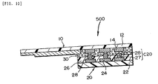
flexible wiring board 500, and FIG. 10 is a cross-sectional view diagrammatically showing theflexible wiring board 500, taken along line B-B in FIG. 9. In this example, components having the same functions as of those of the components in the above-referencedflexible wiring board 100 are designated with substantially the same reference numerals, and the detailed discussion thereabout is omitted here. - A
flexible wiring board 500 in this modification is different from theflexible wiring board 100 shown in FIG. 1 and FIG. 2 in that a portion of the second single-sidedflexible board 20 is bonded to the first single-sidedflexible board 10. The second single-sidedflexible board 20 forms a branch wiring section, the free end of which is provided with a secondoutput terminal region 15C. As shown in FIG. 10, the first single-sidedflexible board 10 has no first insulating layer. - In this modification, the second single-sided
flexible board 20 forming the branch wiring section has, on the end thereof, agrip portion 29 for handling. Thegrip portion 29 is formed to project in the direction opposite from the first single-sidedflexible board 10. It is sufficient if thegrip portion 29 is supported or clamped, mechanically or manually, in a bonding step for bonding the secondoutput terminal region 15C to a joint portion, and the size and the shape of thegrip portion 29 are not limited to any particular ones. Preferably, thegrip portion 29 has no wiring therewithin to prevent mechanical damage on the wiring. With thegrip portion 29 formed on the second single-sidedflexible board 20, the second single-sidedflexible board 20 is bonded to the predetermined area while being positioned easily with a good accuracy. - Besides the operation and advantages of the
flexible wiring board 100, theflexible wiring board 500 can make connection at the two terminal regions of a unit to be connected (an electrooptical device to be discussed later, for example), thereby presenting a compact wiring structure. Specifically, when theflexible wiring board 500 is applied to an electrooptical device, theoutput terminal region 15B of the first single-sidedflexible board 10 is used as a wiring for signals for the electrooptical device, while theoutput terminal region 15C of the second single-sidedflexible board 20 is used for a wiring for scanning. - An embodiment of the present invention is a liquid-crystal display device, as an example of an electrooptical device in which the flexible wiring board of the present invention is incorporated. FIG. 6 is a plan view diagrammatically showing a liquid-
crystal display device 1000 of this embodiment. - The liquid-
crystal display device 1000 is a passive-matrix, reflective-type liquid-crystal display device. The liquid-crystal display device 1000 includes a liquid-crystal display panel 2 and a printed board 3. The liquid-crystal display panel 2 and the printed board 3 are connected to each other through a firstflexible wiring board 100 and a secondflexible wiring board 5 of the present invention. - The liquid-
crystal display panel 2 includes a pair of opposingglass substrates glass substrates substrates glass substrates glass substrate 6, facing theglass substrate 7. A plurality of scanning electrodes 9, extending in a direction perpendicular to the signal electrodes 8, are formed on the surface of theglass substrate 7, facing theglass substrate 6. - In one predetermined edge portion (a lower edge portion in FIG. 6) of the liquid-
crystal display panel 2, the edge of theglass substrate 6 is designed to project out of the edge of theglass substrate 7 laterally (downward in FIG. 6), and the projecting portion (the area where theglass substrate 6 does not overlap the glass substrate 7) forms a wiringjoint section 6A. In another edge portion (on a left-side edge portion in FIG. 6), next to the above-referenced edge portion of the liquid-crystal display panel 2, the edge of theother glass substrate 7 projects out of the edge of the oneglass substrate 6 laterally (leftward in FIG. 6), and a wiringjoint section 7A is thus formed. Signal drivers IC200 and IC300 are COG (Chip On Glass) mounted on the wiringjoint section 6A of theglass substrate 6. These signal drivers IC200 and IC300 are connected to anoutput terminal section 8A to which the plurality of the signal electrodes 8 extend, and are also connected to inputterminals joint section 6A. A scanning driver IC400 is COG-mounted on the wiringjoint section 7A of theglass substrate 7. The scanning driver IC400 is connected to theoutput terminal section 9A to which the plurality of the scanning electrodes 9 extend and is connected to inputterminals 410 arranged on the edge portion of the wiringjoint section 7A. - The
output terminal region 15B of the firstflexible wiring board 100 is bonded, using an anisotropically conductive film (ACF), to be electrically connected to the plurality of theinput terminals joint section 6A of theglass substrate 6. Similarly, theoutput terminal section 5A of the secondflexible wiring board 5 is bonded, using an anisotropically conductive film, to be electrically connected to the plurality ofinput terminals 410 arranged along the long side of wiringjoint section 7A of theglass substrate 7. Theinput terminal region 15A of the firstflexible wiring board 100 is bonded to theoutput terminal region 3A formed in the printed board 3 using an anisotropically conductive film. Theinput terminal region 5B of the secondflexible wiring board 5 is bonded to the output terminal region 3B formed in the printed board 3 using an anisotropically conductive film. A predetermined wiring is formed on the printed board 3 and a diversity of electronic components is mounted on the printed board 3 to control and drive the liquid-crystal display panel 2. - Some electronic equipment employing the liquid-crystal display device thus constructed may be provided with an input unit such as a keyboard or numerical keys, and presents data on a liquid-crystal display panel in response to an input operation to the input unit. In such electronic equipment, the liquid-crystal display panel and a printed board are assembled in a chassis (a panel housing frame). Two
flexible wiring boards - The electrooptical device of the present invention includes the flexible wiring board of the present invention, and implements low-cost and thin-structure design, taking advantage of the operation and advantage of the above-referenced flexible wiring board.
- Examples of electronic equipment incorporating a liquid-crystal display device as the electrooptical device of the present invention are now discussed.
- Discussed here is a digital still camera in which the liquid-crystal display unit of the present invention is incorporated as a finder. FIG. 7 is a perspective view showing the construction of the digital still camera, and also simply showing a connection with external devices.
- Ordinary cameras expose a film to the image of a subject, while a
digital still camera 1200 produces a video signal by photoelectrically converting the image of a subject through an image pickup device such as a CCD (Charge Coupled-Device). Thedigital still camera 1200 includes a liquid crystal panel of the above-referenced liquid-crystal display unit 1000, behind a case 1202 (in front of thecase 1202 in FIG. 7), and presents a display in accordance with the video signal from the CCD. The liquid-crystal display unit 1000 functions as a finder for presenting the image of the subject. Alight receiving unit 1204, including an optical lens and the CCD, is arranged on the front of the case 1202 (on the back of thecase 1202 in FIG. 7). - When a photographer presses a
shutter button 1206 recognizing the subject image presented on the liquid-crystal display unit 1000, the video signal on the CCD at the moment is transferred to and stored in a memory in acircuit board 1208. In thedigital still camera 1200, videosignal output terminals 1212 and an input/output terminal 1214 for data communication are provided on one side surface of thecase 1202. As shown in FIG. 7, as necessary, atelevision monitor 1300 is connected to the videosignal output terminals 1212, and apersonal computer 1400 is connected to the input/output terminal 1214 for data communication. In response to predetermined operations, the video signal stored in the memory in thecircuit board 1208 is output to thetelevision monitor 1300 or thepersonal computer 1400. - FIGS. 8(A), 8(B) and 8(C) are external views of electronic equipment which incorporates a liquid-crystal display unit as the electrooptical device of the present invention. FIG. 8(A) shows a
portable telephone 3000, which includes the liquid-crystal display unit 1000 on the upper front surface thereof. FIG. 8(B) shows awristwatch 4000, which includes the liquid-crystal display unit 1000 on the center front thereof. FIG. 8(C) showsportable information equipment 5000, which includes the liquid-crystal display unit 1000 as a display and aninput unit 5100. - Besides the liquid-
crystal display unit 1000, these pieces of electronic equipment include a variety of circuits, such as a display information output source, a display information processing circuit, a clock generator circuit, and a display signal generator unit including a power source circuit for supplying these circuits with power. The display presents a video image in theportable information equipment 5000, when it is supplied with the video signal generated by the display signal generator in response to information from theinput unit 5100. - Electronic equipment which incorporates the liquid-
crystal display unit 1000 of the present invention is not limited to the digital still camera, the portable telephone, the wristwatch, and the portable information equipment, and may be any of diversity of electronic equipment, such as electronic pocketbook, pager, POS terminal, IC card, mini disc player, liquid-crystal projector, multi-media personal computer (PC), engineering workstation (EWS), notebook type personal computer, word processor, television, viewfinder type or direct-monitor viewing type video tape recorder, electronic pocketbook, electronic tabletop calculator, car navigation system, apparatus having a touch panel, and clock. - From the standpoint of driving method, the liquid-crystal display panel employed may be a passive matrix display panel or a static driving liquid-crystal display panel with no switching device incorporated therewithin, or an active matrix addressing liquid-crystal display panel with a three-terminal switching device, represented by a TFT (thin-film transistor) or a two-terminal switching device represented by a TFD (thin-film diode) incorporated therewithin, and from the standpoint of electrooptical characteristics, a diversity of liquid-crystal display panels may be employed including the one of a TN type, STN type, a guest-host type, a phase-change type, or a ferroelectric type.
- The devices of the present invention have been discussed in connection with several specific embodiments, and changes may be made in the present invention without departing from the scope of the present invention. The above-referenced embodiments employ the liquid-crystal display device as video display means of the electrooptical device (an electrooptical display unit), but the present invention is not limited to this display, and the present invention may be applied to a variety of electrooptical means, such as a flat CRT, a compact television set employing a liquid-crystal shutter, electroluminescence, plasma display, CRT display, or FED (Field Emission Display).
Claims (12)
- A flexible wiring board comprising a first single-sided flexible board and a second single-sided flexible board,wherein the first single-sided flexible board comprises a first base body having an insulative property, and a first wiring layer formed in a predetermined pattern on the first base body,the second single-sided flexible board comprises a second base body having an insulative property, and a second wiring layer formed in a predetermined pattern on the second base body,an insulating layer for covering the wiring layer is formed on at least one of the first and second single-sided flexible boards, a hole, forming a contact section, is created in the insulating layer to electrically connect the first wiring layer and the second wiring layer within a predetermined area, andthe first single-sided flexible board and the second single-sided flexible board are arranged with the first wiring layer and the second wiring layer in a facing state, and are bonded through an anisotropically conductive adhesive layer.
- A flexible wiring board according to Claim 1, wherein the second single-sided flexible board is arranged on a portion of the first single-sided flexible board.
- A flexible wiring board according to one of Claims 1 and 2, wherein the first single-sided flexible board has a shape matching the general configuration of the flexible wiring board.
- A flexible wiring board according to one of Claims 1 and 2, wherein a portion of the second single-sided flexible board is bonded onto the first single-sided flexible board while the remaining portion thereof remains unbonded to the first single-sided flexible board.
- A flexible wiring board according to one of Claims 1 through 3, wherein the first single-sided flexible board comprises an input terminal region and an output terminal region.
- A flexible wiring board according to Claim 4, wherein the first single-sided flexible board comprises an input terminal region and a first output terminal region, and the second single-sided flexible board comprises a second output terminal region.
- A flexible wiring board according to one of Claims 1 through 6, wherein the contact section comprises a bump within the hole.
- A flexible wiring board according to one of Claims 1 through 7, wherein the first single-sided flexible board and the second single-sided flexible board respectively comprise the insulating layers.
- A flexible wiring board according to one of Claims 1 through 8, wherein the anisotropically conductive adhesive layer is formed by thermocompression bonding the first single-sided flexible board and the second single-sided flexible board with an anisotropically conductive film interposed therebetween.
- An electrooptical device comprising an electrooptical panel comprising an electrooptical material layer between mutually opposing first and second substrates,wherein the first substrate comprises a first wiring bonding region which does not overlap the second substrate,the second substrate comprises a second wiring bonding region which does not overlap the first substrate, andat least one of the first wiring bonding region and the second wiring bonding region is connected to the flexible wiring board according to one of Claims 1 through 9.
- An electrooptical device according to Claim 10, wherein the electrooptical material layer is a liquid-crystal layer.
- Electronic equipment comprising the electrooptical device according to one of Claims 10 and 11.
Applications Claiming Priority (2)
| Application Number | Priority Date | Filing Date | Title |
|---|---|---|---|
| JP24946399A JP2001077501A (en) | 1999-09-03 | 1999-09-03 | Flexible wiring board, optoelectronic device and electronic apparatus |
| JP24946399 | 1999-09-03 |
Publications (3)
| Publication Number | Publication Date |
|---|---|
| EP1081991A2 true EP1081991A2 (en) | 2001-03-07 |
| EP1081991A3 EP1081991A3 (en) | 2003-04-02 |
| EP1081991B1 EP1081991B1 (en) | 2006-07-26 |
Family
ID=17193344
Family Applications (1)
| Application Number | Title | Priority Date | Filing Date |
|---|---|---|---|
| EP00307577A Expired - Lifetime EP1081991B1 (en) | 1999-09-03 | 2000-09-01 | Flexible wiring board, electro-optical device and electronic equipment |
Country Status (7)
| Country | Link |
|---|---|
| US (1) | US6506978B1 (en) |
| EP (1) | EP1081991B1 (en) |
| JP (1) | JP2001077501A (en) |
| KR (1) | KR100393948B1 (en) |
| CN (1) | CN1160588C (en) |
| DE (1) | DE60029524T2 (en) |
| TW (1) | TW548497B (en) |
Cited By (3)
| Publication number | Priority date | Publication date | Assignee | Title |
|---|---|---|---|---|
| CN103607855A (en) * | 2013-10-26 | 2014-02-26 | 溧阳市东大技术转移中心有限公司 | Method for manufacturing composite flexible printed circuit board |
| CN106507613A (en) * | 2016-10-11 | 2017-03-15 | 江苏博敏电子有限公司 | A kind of HDI method for manufacturing circuit board of employing conductive polymer polymerization technique |
| CN114199898A (en) * | 2021-12-01 | 2022-03-18 | 深圳市鑫达辉软性电路科技有限公司 | Multi-layer board AOI (automatic optical inspection) avoiding scanning structure, configuration method and scanning method |
Families Citing this family (34)
| Publication number | Priority date | Publication date | Assignee | Title |
|---|---|---|---|---|
| JP3729092B2 (en) * | 2001-06-19 | 2005-12-21 | ソニー株式会社 | Conductive bonding material, multilayer printed wiring board, and method for manufacturing multilayer printed wiring board |
| JP2003298232A (en) * | 2002-04-02 | 2003-10-17 | Sony Corp | Multilayer wiring board and method of manufacturing the same |
| US6823582B1 (en) | 2002-08-02 | 2004-11-30 | National Semiconductor Corporation | Apparatus and method for force mounting semiconductor packages to printed circuit boards |
| US6864586B2 (en) * | 2003-02-28 | 2005-03-08 | Silicon Integrated Systems Corp. | Padless high density circuit board |
| US8518304B1 (en) | 2003-03-31 | 2013-08-27 | The Research Foundation Of State University Of New York | Nano-structure enhancements for anisotropic conductive material and thermal interposers |
| US7378596B2 (en) | 2003-04-18 | 2008-05-27 | Ibiden Co., Ltd. | Rigid-flex wiring board |
| KR20050035970A (en) * | 2003-10-14 | 2005-04-20 | 삼성전자주식회사 | Flexible printed circuit board and liquid crystal display device using the same |
| US20050265650A1 (en) * | 2004-05-27 | 2005-12-01 | Sunil Priyadarshi | Small profile, pluggable optical transceiver subassembly |
| JP4536430B2 (en) | 2004-06-10 | 2010-09-01 | イビデン株式会社 | Flex rigid wiring board |
| KR100594299B1 (en) * | 2004-10-29 | 2006-06-30 | 삼성전자주식회사 | Flexible printed circuit, and hard disk drive comprising the same |
| US20060139551A1 (en) * | 2004-12-27 | 2006-06-29 | Yohei Kimura | Display device |
| JP4699136B2 (en) * | 2005-08-17 | 2011-06-08 | 日本メクトロン株式会社 | Method for manufacturing flexible printed circuit board |
| KR100684726B1 (en) * | 2005-09-27 | 2007-02-20 | 삼성에스디아이 주식회사 | Plasma display device |
| TWI434119B (en) * | 2006-06-28 | 2014-04-11 | Creator Technology Bv | Improved common contact layout for flexible displays |
| US8320133B1 (en) * | 2006-12-05 | 2012-11-27 | Raytheon Company | Rigid/flexible circuit board |
| JP5525692B2 (en) * | 2007-02-22 | 2014-06-18 | 三星ディスプレイ株式會社 | Display substrate, manufacturing method thereof, and display device including the same |
| KR101365118B1 (en) * | 2007-02-22 | 2014-02-25 | 삼성디스플레이 주식회사 | Display substrate, method of manufacturing the same and display device having the display substrate |
| JP2008277508A (en) * | 2007-04-27 | 2008-11-13 | Matsushita Electric Ind Co Ltd | Flexible circuit board, and motor and hard disc drive device equipped with the board |
| WO2008149443A1 (en) * | 2007-06-07 | 2008-12-11 | Hitachi, Ltd. | Flexible wiring board and plasma display device using the same |
| JP5184335B2 (en) * | 2008-12-26 | 2013-04-17 | 株式会社フジクラ | Printed wiring board, manufacturing method thereof, and connection method of printed wiring board |
| TW201124007A (en) * | 2009-12-30 | 2011-07-01 | Au Optronics Corp | Substrate and substrate bonding device using the same |
| CN103517558B (en) * | 2012-06-20 | 2017-03-22 | 碁鼎科技秦皇岛有限公司 | Manufacture method for package substrate |
| CN103607839A (en) * | 2013-10-26 | 2014-02-26 | 溧阳市东大技术转移中心有限公司 | Composite flexible substrate |
| CN104093263B (en) * | 2014-05-19 | 2018-08-14 | 北京国联万众半导体科技有限公司 | Bridge module and board unit for flexible base board |
| JP6518451B2 (en) * | 2015-02-02 | 2019-05-22 | 株式会社フジクラ | Elastic circuit board |
| CN107211548B (en) * | 2015-02-13 | 2021-10-29 | Pi-克瑞斯托株式会社 | Method for forming laminated circuit board and laminated circuit board formed thereby |
| JP2016178121A (en) * | 2015-03-18 | 2016-10-06 | タツタ電線株式会社 | Stretchable cable and stretchable circuit board |
| KR102593532B1 (en) * | 2016-06-03 | 2023-10-26 | 삼성디스플레이 주식회사 | Anisotropic conductive film and display device using the same |
| JPWO2018168627A1 (en) * | 2017-03-14 | 2020-01-16 | パナソニックIpマネジメント株式会社 | Touch sensor |
| US11500489B2 (en) | 2019-01-30 | 2022-11-15 | Chengdu Boe Optoelectronics Technology Co., Ltd. | Flexible circuit board and manufacturing method, display device, circuit board structure and display panel thereof |
| JP6930681B2 (en) * | 2019-03-25 | 2021-09-01 | 株式会社村田製作所 | Elastic mounting board |
| CN110346957A (en) * | 2019-06-27 | 2019-10-18 | 深圳市华星光电技术有限公司 | Liquid crystal module and preparation method thereof |
| CN111399290B (en) * | 2020-04-26 | 2022-11-08 | 上海中航光电子有限公司 | Display panel and display device |
| CN111511098B (en) * | 2020-06-10 | 2021-08-20 | 京东方科技集团股份有限公司 | Flexible Printed Circuit (FPC) and display device |
Citations (6)
| Publication number | Priority date | Publication date | Assignee | Title |
|---|---|---|---|---|
| JPH06202135A (en) * | 1993-01-05 | 1994-07-22 | Nec Corp | Liquid crystal display device |
| US5527998A (en) * | 1993-10-22 | 1996-06-18 | Sheldahl, Inc. | Flexible multilayer printed circuit boards and methods of manufacture |
| US5686702A (en) * | 1991-07-26 | 1997-11-11 | Nippon Electric Co | Polyimide multilayer wiring substrate |
| JPH09318965A (en) * | 1996-05-30 | 1997-12-12 | Nippon Seiki Co Ltd | Liquid crystal display device |
| US5719749A (en) * | 1994-09-26 | 1998-02-17 | Sheldahl, Inc. | Printed circuit assembly with fine pitch flexible printed circuit overlay mounted to printed circuit board |
| US5727310A (en) * | 1993-01-08 | 1998-03-17 | Sheldahl, Inc. | Method of manufacturing a multilayer electronic circuit |
Family Cites Families (14)
| Publication number | Priority date | Publication date | Assignee | Title |
|---|---|---|---|---|
| US4659872A (en) * | 1985-04-30 | 1987-04-21 | Amp Incorporated | Flexible flat multiconductor cable |
| US4740657A (en) * | 1986-02-14 | 1988-04-26 | Hitachi, Chemical Company, Ltd | Anisotropic-electroconductive adhesive composition, method for connecting circuits using the same, and connected circuit structure thus obtained |
| JPH0738502B2 (en) * | 1989-10-17 | 1995-04-26 | シャープ株式会社 | Circuit board connection method |
| JP2543281B2 (en) | 1992-03-02 | 1996-10-16 | 松下電器産業株式会社 | Liquid crystal display panel and display device |
| JPH0637451A (en) | 1992-07-20 | 1994-02-10 | Hitachi Chem Co Ltd | Multilayer printed wiring board and manufacture thereof |
| JP3415845B2 (en) * | 1993-07-27 | 2003-06-09 | シチズン時計株式会社 | Electrical connection structure and electrical connection method thereof |
| JP2867209B2 (en) * | 1993-08-27 | 1999-03-08 | 日東電工株式会社 | Method of connecting flexible circuit board to contact object and structure thereof |
| US5893623A (en) * | 1993-11-12 | 1999-04-13 | Seiko Epson Corporation | Structure and method for mounting semiconductor devices, and liquid crystal display |
| US5661042A (en) * | 1995-08-28 | 1997-08-26 | Motorola, Inc. | Process for electrically connecting electrical devices using a conductive anisotropic material |
| KR100232680B1 (en) * | 1997-01-22 | 1999-12-01 | 구본준 | Acf structure |
| JPH10261849A (en) * | 1997-03-19 | 1998-09-29 | Fujitsu Ltd | Flexible printed board and connection printed board structure |
| KR100269947B1 (en) * | 1997-09-13 | 2000-10-16 | 윤종용 | Printed circuit board and LCD module using it |
| US6063647A (en) * | 1997-12-08 | 2000-05-16 | 3M Innovative Properties Company | Method for making circuit elements for a z-axis interconnect |
| JP2000208698A (en) * | 1999-01-18 | 2000-07-28 | Toshiba Corp | Semiconductor device |
-
1999
- 1999-09-03 JP JP24946399A patent/JP2001077501A/en active Pending
-
2000
- 2000-07-24 TW TW089114757A patent/TW548497B/en not_active IP Right Cessation
- 2000-08-31 KR KR10-2000-0051028A patent/KR100393948B1/en active IP Right Grant
- 2000-09-01 US US09/654,119 patent/US6506978B1/en not_active Expired - Lifetime
- 2000-09-01 CN CNB001268821A patent/CN1160588C/en not_active Expired - Lifetime
- 2000-09-01 EP EP00307577A patent/EP1081991B1/en not_active Expired - Lifetime
- 2000-09-01 DE DE60029524T patent/DE60029524T2/en not_active Expired - Lifetime
Patent Citations (6)
| Publication number | Priority date | Publication date | Assignee | Title |
|---|---|---|---|---|
| US5686702A (en) * | 1991-07-26 | 1997-11-11 | Nippon Electric Co | Polyimide multilayer wiring substrate |
| JPH06202135A (en) * | 1993-01-05 | 1994-07-22 | Nec Corp | Liquid crystal display device |
| US5727310A (en) * | 1993-01-08 | 1998-03-17 | Sheldahl, Inc. | Method of manufacturing a multilayer electronic circuit |
| US5527998A (en) * | 1993-10-22 | 1996-06-18 | Sheldahl, Inc. | Flexible multilayer printed circuit boards and methods of manufacture |
| US5719749A (en) * | 1994-09-26 | 1998-02-17 | Sheldahl, Inc. | Printed circuit assembly with fine pitch flexible printed circuit overlay mounted to printed circuit board |
| JPH09318965A (en) * | 1996-05-30 | 1997-12-12 | Nippon Seiki Co Ltd | Liquid crystal display device |
Non-Patent Citations (2)
| Title |
|---|
| PATENT ABSTRACTS OF JAPAN vol. 018, no. 557 (P-1817), 24 October 1994 (1994-10-24) & JP 06 202135 A (NEC CORP), 22 July 1994 (1994-07-22) * |
| PATENT ABSTRACTS OF JAPAN vol. 1998, no. 04, 31 March 1998 (1998-03-31) & JP 09 318965 A (NIPPON SEIKI CO LTD), 12 December 1997 (1997-12-12) * |
Cited By (4)
| Publication number | Priority date | Publication date | Assignee | Title |
|---|---|---|---|---|
| CN103607855A (en) * | 2013-10-26 | 2014-02-26 | 溧阳市东大技术转移中心有限公司 | Method for manufacturing composite flexible printed circuit board |
| CN103607855B (en) * | 2013-10-26 | 2016-06-08 | 溧阳市东大技术转移中心有限公司 | The manufacture method of a kind of composite flexible substrate |
| CN106507613A (en) * | 2016-10-11 | 2017-03-15 | 江苏博敏电子有限公司 | A kind of HDI method for manufacturing circuit board of employing conductive polymer polymerization technique |
| CN114199898A (en) * | 2021-12-01 | 2022-03-18 | 深圳市鑫达辉软性电路科技有限公司 | Multi-layer board AOI (automatic optical inspection) avoiding scanning structure, configuration method and scanning method |
Also Published As
| Publication number | Publication date |
|---|---|
| CN1287285A (en) | 2001-03-14 |
| US6506978B1 (en) | 2003-01-14 |
| EP1081991B1 (en) | 2006-07-26 |
| JP2001077501A (en) | 2001-03-23 |
| KR20010030190A (en) | 2001-04-16 |
| KR100393948B1 (en) | 2003-08-09 |
| TW548497B (en) | 2003-08-21 |
| DE60029524D1 (en) | 2006-09-07 |
| DE60029524T2 (en) | 2007-07-26 |
| EP1081991A3 (en) | 2003-04-02 |
| CN1160588C (en) | 2004-08-04 |
Similar Documents
| Publication | Publication Date | Title |
|---|---|---|
| EP1081991B1 (en) | Flexible wiring board, electro-optical device and electronic equipment | |
| US6972966B1 (en) | Composite flexible wiring board, method of manufacturing the same, electro-optical device, and electronic equipment | |
| US6448663B1 (en) | Semiconductor device, semiconductor device mounting structure, liquid crystal device, and electronic apparatus | |
| US7948768B2 (en) | Tape circuit substrate with reduced size of base film | |
| US6617521B1 (en) | Circuit board and display device using the same and electronic equipment | |
| US7202597B2 (en) | Pixel element substrate, display device, electronic device, and method for manufacturing the pixel element substrate | |
| US6519021B1 (en) | Wiring board for connection of electro-optical panel, electro-optical device and electronic apparatus | |
| US7233382B2 (en) | LCD connected to additional LCD through multiple flexible printed circuit boards | |
| JP2003273476A (en) | Mounting structure and method of manufacturing the same, electro-optical device and electronic device | |
| JP2000294897A (en) | Circuit board, display device using the same and electronics | |
| KR20040088347A (en) | Electro-optical device, electronic instrument having the same, and manufacturing method of the same | |
| JP2001119120A (en) | Flexible wiring board package and method for manufacturing the same | |
| JP2003273486A (en) | Packaging structure body and manufacturing method thereof, electro-optic device, and electronic equipment | |
| JP2002289764A (en) | Flexible circuit board, display device using it and electronic equipment | |
| JP2920843B2 (en) | Liquid crystal display | |
| JP3653981B2 (en) | Mounting structure of liquid crystal device and electronic device | |
| JP2001075493A (en) | Electro-optic device and its production as well as electronic apparatus | |
| JP2000058985A (en) | Wiring board, liquid crystal device, and electronic equipment | |
| JP2004186472A (en) | Mounting structure, its manufacturing method, electro-optical device, and electronic instrument | |
| JP3852305B2 (en) | EL element driving circuit, EL element driving method, and electronic apparatus | |
| JPH07239479A (en) | Liquid crystal display element | |
| JP2002072241A (en) | Wiring board for connecting optoelectronic panel, optoelectronic device, and electronic equipment | |
| JP2000250058A (en) | Electrooptical device | |
| JP2002023189A (en) | Wiring board for connecting electro-optical panel | |
| JP2002072240A (en) | Wiring board for connecting optoelectronic panel, optoelectronic device, and electronic equipment |
Legal Events
| Date | Code | Title | Description |
|---|---|---|---|
| PUAI | Public reference made under article 153(3) epc to a published international application that has entered the european phase |
Free format text: ORIGINAL CODE: 0009012 |
|
| AK | Designated contracting states |
Kind code of ref document: A2 Designated state(s): AT BE CH CY DE DK ES FI FR GB GR IE IT LI LU MC NL PT SE |
|
| AX | Request for extension of the european patent |
Free format text: AL;LT;LV;MK;RO;SI |
|
| PUAL | Search report despatched |
Free format text: ORIGINAL CODE: 0009013 |
|
| AK | Designated contracting states |
Kind code of ref document: A3 Designated state(s): AT BE CH CY DE DK ES FI FR GB GR IE IT LI LU MC NL PT SE |
|
| AX | Request for extension of the european patent |
Extension state: AL LT LV MK RO SI |
|
| 17P | Request for examination filed |
Effective date: 20031001 |
|
| AKX | Designation fees paid |
Designated state(s): DE FR GB |
|
| 17Q | First examination report despatched |
Effective date: 20050512 |
|
| GRAP | Despatch of communication of intention to grant a patent |
Free format text: ORIGINAL CODE: EPIDOSNIGR1 |
|
| GRAS | Grant fee paid |
Free format text: ORIGINAL CODE: EPIDOSNIGR3 |
|
| GRAA | (expected) grant |
Free format text: ORIGINAL CODE: 0009210 |
|
| AK | Designated contracting states |
Kind code of ref document: B1 Designated state(s): DE FR GB |
|
| REG | Reference to a national code |
Ref country code: GB Ref legal event code: FG4D |
|
| REF | Corresponds to: |
Ref document number: 60029524 Country of ref document: DE Date of ref document: 20060907 Kind code of ref document: P |
|
| ET | Fr: translation filed | ||
| PLBE | No opposition filed within time limit |
Free format text: ORIGINAL CODE: 0009261 |
|
| STAA | Information on the status of an ep patent application or granted ep patent |
Free format text: STATUS: NO OPPOSITION FILED WITHIN TIME LIMIT |
|
| 26N | No opposition filed |
Effective date: 20070427 |
|
| REG | Reference to a national code |
Ref country code: FR Ref legal event code: PLFP Year of fee payment: 16 |
|
| REG | Reference to a national code |
Ref country code: DE Ref legal event code: R082 Ref document number: 60029524 Country of ref document: DE Representative=s name: WEICKMANN & WEICKMANN PATENTANWAELTE - RECHTSA, DE Ref country code: DE Ref legal event code: R081 Ref document number: 60029524 Country of ref document: DE Owner name: BOE TECHNOLOGY GROUP CO., LTD., CN Free format text: FORMER OWNER: BOE TECHNOLOGY (HK) LIMITED, HONG KONG, HK Ref country code: DE Ref legal event code: R081 Ref document number: 60029524 Country of ref document: DE Owner name: BOE TECHNOLOGY GROUP CO., LTD., CN Free format text: FORMER OWNER: SEIKO EPSON CORP., TOKYO, JP Ref country code: DE Ref legal event code: R082 Ref document number: 60029524 Country of ref document: DE Representative=s name: WEICKMANN & WEICKMANN PATENT- UND RECHTSANWAEL, DE |
|
| REG | Reference to a national code |
Ref country code: GB Ref legal event code: 732E Free format text: REGISTERED BETWEEN 20160218 AND 20160224 |
|
| REG | Reference to a national code |
Ref country code: FR Ref legal event code: TP Owner name: BOE TECHNOLOGY GROUP CO., LTD., CN Effective date: 20160405 |
|
| REG | Reference to a national code |
Ref country code: FR Ref legal event code: PLFP Year of fee payment: 17 |
|
| REG | Reference to a national code |
Ref country code: FR Ref legal event code: PLFP Year of fee payment: 18 |
|
| REG | Reference to a national code |
Ref country code: FR Ref legal event code: PLFP Year of fee payment: 19 |
|
| PGFP | Annual fee paid to national office [announced via postgrant information from national office to epo] |
Ref country code: DE Payment date: 20190820 Year of fee payment: 20 Ref country code: FR Payment date: 20190730 Year of fee payment: 20 |
|
| PGFP | Annual fee paid to national office [announced via postgrant information from national office to epo] |
Ref country code: GB Payment date: 20190830 Year of fee payment: 20 |
|
| REG | Reference to a national code |
Ref country code: DE Ref legal event code: R071 Ref document number: 60029524 Country of ref document: DE |
|
| REG | Reference to a national code |
Ref country code: GB Ref legal event code: PE20 Expiry date: 20200831 |
|
| PG25 | Lapsed in a contracting state [announced via postgrant information from national office to epo] |
Ref country code: GB Free format text: LAPSE BECAUSE OF EXPIRATION OF PROTECTION Effective date: 20200831 |