Field of the Invention
-
The present invention relates to a metallization process for manufacturing
semiconductor devices. More particularly, the present invention relates to the metallization
of semiconductor substrates having apertures to form void-free interconnections between
conducting layers, and planar metal surfaces.
Background of the Invention
-
Sub-half micron multilevel metallization is one of the key technologies for the next
generation of very large scale integration ("VLSI"). The multilevel interconnections that
lie at the heart of this technology require planarization of high aspect ratio apertures,
including contacts, vias, lines or other features. Reliable formation of these interconnects
is very important to the success of VLSI and to the continued effort to increase circuit
density and quality on individual substrates and die.
-
Aluminum (Al) or copper (Cu) layers formed by chemical vapor deposition
("CVD"), like other CVD processes, provide good conformal layers, i.e., a uniform
thickness layer on the sides and base of the feature, for very small geometries, including
sub-half micron (<0.5 µm) apertures, at low temperatures. Therefore, CVD processes
(CVD Al or CVD Cu) are common methods used to fill apertures. However, transmission
electron microscopy data ("TEM") has revealed that voids exist in many of the CVD
formed Al apertures even though electric tests of these same apertures do not evidence the
existence of this void. If the layer is subsequently processed, the void can result in a
defective circuit. It should be recognized that this kind of void is very difficult to detect
by regular cross sectional standard electron microscopy ("SEM") techniques, because
some deformation occurs in soft aluminum during mechanical polishing. In addition,
electric conductivity tests do not detect any structural abnormalities. However, despite
generally positive electric conductivity tests, conduction through the contact having the
void may, over time, compromise the integrity of the integrated circuit devices.
-
A TEM study of various CVD Al layers formed on substrates indicates that the
formation of voids occurs through a key hole process wherein the top portion of the via
becomes sealed before the via has been entirely filled. Although a thin conformal layer of
CVD Al can typically be deposited in high aspect ratio contacts and vias at low
temperatures, continued CVD deposition to complete filling of the contacts or vias
typically results in the formation of voids therein. Extensive efforts have been focused on
elimination of voids in metal layers by modifying CVD processing conditions.
-
An alternative technique for metallization of high aspect ratio apertures, is hot
planarization of aluminum through physical vapor deposition ("PVD"). The first step in
this process requires deposition of a thin layer of a refractory metal such as titanium (Ti)
on a patterned wafer to form a barrier/wetting layer which facilitates flow of the Al during
the PVD process. Following deposition of the barrier/wetting layer, the next step requires
deposition of either (1) a hot PVD Al layer or (2) a cold PVD Al layer followed by a hot
PVD Al layer onto the wetting layer. However, hot PVD Al processes are very sensitive
to the quality of the wetting layer, wafer condition, and other processing parameters.
Small variations in processing conditions and/or poor coverage of the wetting layer can
result in incomplete filling of the contacts or vias, thus creating voids. In order to reliably
fill the vias and contacts, hot PVD Al processes must be performed at temperatures above
about 450°C. Even at higher temperatures, PVD processes may result in a bridging effect
whereby the mouth of the contact or via is closed because the deposition layer formed on
the top surface of the substrate and the upper walls of the contact or via join before the
floor of the contact or via has been completely filled.
-
Once a PVD Al layer has been deposited onto the substrate, reflow of the Al may
occur by directing ion bombardment towards the substrate itself. Bombarding the
substrate with ions causes the metal layer formed on the substrate to reflow. This process
typically heats the metal layer as a result of the energy created by the plasma and resulting
collisions of ions onto the metal layer. The high temperatures generated in the metal
layers formed on the substrate compromises the integrity of devices having sub-half
micron geometries. Therefore, heating of the metal layers is disfavored in these
applications.
-
U.S. Patent No.5,147,819 ("the '819 patent") discloses a process for filling vias
that involves applying a CVD Al layer with a thickness of from 5 percent to 35 percent of
the defined contact or via diameter to improve step coverage, then applying a sufficiently
thick PVD Al layer to achieve a predetermined overall layer thickness. A high energy laser
beam is then used to melt the intermixed CVD Al and PVD Al and thereby achieve
improved step coverage and planarization. However, this process requires heating the
wafer surface to a temperature no less than 660°C. Such a high temperature is not
acceptable for most sub-half micron technology. Furthermore, the use of laser beams
scanned over a wafer may affect the reflectivity and uniformity of the metal layer.
-
Other attempts at filling high aspect ratio sub-half micron contacts and vias using
known reflow or planarization processes at lower temperatures have resulted in dewetting
of the CVD Al from the silicon dioxide (SiO2) substrate and the formation of
discontinuous islands on the side walls of the vias. Furthermore, in order for the CVD Al
to resist dewetting at lower temperatures, the thickness of the CVD Al has to be several
thousand Angstroms (A). Since ten thousand Angstroms equal one micron, a CVD Al
layer of several thousand Angstroms on the walls of a sub-half micron via will completely
seal the via and form voids therein.
-
U.S. Patent No. 5,665,659, describes a method for forming a metal layer on a
semiconductor substrate including depositing a barrier/wetting layer, heat treating the
substrate for a predetermined time at an intermediate temperature between 200°C and
400°C, and then depositing a PVD metal layer on the semiconductor substrate at a
temperature below 200°C and a pressure below about 2 milliTorr. The deposited metal
layer is then thermally treated at a temperature between 0.6 Tm-1.0 Tm (where Tm is the
melting point of the metal layer) to reflow the metal layer. The barrier/wetting layer is heat
treated and the metal layer is carefully cooled to reduce formation of grooves on the metal
layer surface.
-
There remains a need for a metallization process for filling apertures, particularly
high aspect ratio sub-half micron contacts and vias, with metal such as aluminum. More
particularly, it would be desirable to have a PVD process for filling such contacts and vias.
Summary of the Invention
-
The present invention provides a metallization process for filling apertures on a
substrate. First, a thin refractory layer is deposited on a substrate followed by depositing a
PVD metal layer at a pressure less than about 1milliTorr to form a conformal layer. The
conformal PVD metal layer does not fill the apertures. Then a bulk PVD metal is
deposited on the substrate and heated to reflow the metal and fill the apertures.
-
In one aspect of the invention, a barrier layer is deposited onto a substrate having
high aspect ratio contacts or vias formed thereon. A titanium or titanium/titanium nitride
barrier layer is preferred for deposition of aluminum. A conformal aluminum layer is then
deposited onto the barrier layer by physical vapor deposition at a pressure less than about
1 milliTorr, preferably less than about 0.35 milliTorr. The conformal aluminum layer is
preferably deposited in a sputtering chamber having a target positioned at least about 100
mm from a substrate. Next, aluminum is deposited by physical vapor deposition onto the
conformal aluminum layer and the via is filled by reflow or annealing of the deposited
aluminum.
-
In another aspect of the invention, the metallization process is carried out in an
integrated processing system that includes PVD chambers for depositing a metal such as
aluminum without the formation of an oxide layer over the aluminum layers. The
processing system may also contain reflow chambers, preclean chambers, and barrier layer
chambers associated with deposition of the metal layers.
Brief Description of the Drawings
-
So that the manner in which the above recited features, advantages and objects of
the present invention are attained and can be understood in detail, a more particular
description of the invention, briefly summarized above, may be had by reference to the
embodiments thereof which are illustrated in the appended drawings.
-
It is to be noted, however, that the appended drawings illustrate only typical
embodiments of this invention and, therefore, are not to be considered limiting of its
scope, for the invention may admit to other equally effective embodiments.
- Figure 1 is a schematic diagram of a metallized semiconductor substrate via
according to the present invention having a barrier layer and a conformal PVD aluminum
layer;
- Figure 2 is a schematic diagram of a metallized semiconductor substrate via
according to the present invention having a barrier layer and intermixed PVD layers filling
the via;
- Figure 3 is a schematic top view of an integrated multi-chamber apparatus suitable
for depositing a barrier layer and a conformal PVD layer on a semiconductor substrate via,
and suitable for filling the via with PVD metal;
- Figure 4 is a schematic diagram of a PVD chamber suitable for depositing a
conformal metal layer at a pressure less than about 1 milliTorr;
- Figure 5 is a schematic diagram of a PVD chamber suitable for depositing a bulk
metal layer at a pressure greater than about 2 milliTorr; and
- Figure 6 is a simplified block diagram showing the hierarchical control structure of
a computer program suitable for controlling a process of the present invention.
-
Detailed Description of the Invention
-
The present invention provides a method for filling high aspect ratio apertures on
semiconductor substrates with metal, particularly sub-micron aperture including contacts,
vias, lines, or other features. In particular, the invention provides excellent step coverage
for filling high aspect ratio apertures with a conformal layer of metal deposited by PVD at
a pressure less than about 1 milliTorr, preferably less than about 0.35 milliTorr, and a
metal layer deposited by PVD that is heated to fill the apertures. The conformal PVD
metal is preferably deposited on a thin barrier/wetting layer comprised of a refractory
metal and/or conductive metal having a melting point greater than that of the conformal
PVD metal. A barrier layer, such as titanium (Ti) or tantulum (Ta), is preferred to prevent
the diffusion of aluminum or copper into adjacent dielectric materials which can cause
electrical shorts to occur. If the barrier material itself does not provide sufficient wetting,
then a separate wetting layer, such as titanium nitride (TiN) or tantulum nitride (TaN) may
be deposited over the barrier layer prior to PVD metal deposition. Preferably, this process
occurs in an integrated processing system including all metal processing chambers.
-
It has been demonstrated that some metals, such as aluminum (Al) and copper
(Cu), can flow at temperatures below their respective melting points due to the effects of
surface tension. However, these metals have a tendency to dewet from an underlying
dielectric layer at high temperatures. Therefore, the present invention interposes a
barrier/wetting layer between a metal layer and the dielectric to improve the wetting of the
metal. An appropriate barrier/wetting layer is one that wets the metal better than the
dielectric material. It is preferred that the barrier/wetting layer provide improved wetting
even when only a thin barrier/wetting layer is deposited. It follows that a preferred
barrier/wetting layer is formed substantially uniformly over the surface of the dielectric,
including the walls and floor of the apertures.
-
According to the present invention, preferred barrier/wetting layers include such
layers as a refractory (tungsten (W), niobium (Nb), aluminum silicates, etc.), tantalum
(Ta), tantalum nitride (TaN), titanium nitride (TiN), PVD Ti/N2-stuffed, a ternary
compound (such as TiSiN, WSiN, etc.) or a combination of these layers. The most
preferred barrier/wetting materials are Ta and TaN, which typically are provided as a PVD
layer having a thickness between about 800 Å and about 1000 Å, or Ti and TiN, which
typically are provided as either PVD or CVD layers having a thickness between about 100
Å and about 400 Å. The barrier/wetting layer is deposited to form a substantially
continuous cap over the dielectric layer and may be treated with nitrogen to improve
barrier properties or adhesion to adjacent layers. Alternatively, exposed surfaces of silicon
can be treated with nitrogen to form a SixNy layer than is effective as a barrier layer for
copper.
-
Following deposition of the barrier/wetting layer, the substrate is then positioned in
a PVD Cu or PVD Al chamber to deposit a conformal metal layer at a pressure less than
about 1 milliTorr and a substrate to target spacing of at least 100 mm. The chamber is
preferably a PVD chamber operating at a pressure less than about 0.35 milliTorr. The
conformal PVD metal layer has a blanket thickness of from about 200 Å to about 1
micron, preferably from about 4000 Å to about 6000 Å. Side wall thickness is typically
10% to 25% of the blanket thickness. Additional metal is then deposited by PVD in the
same chamber or a different chamber and heated to reflow the deposited metal and fill the
apertures leaving a planar surface that does not have grooves.
-
It is also preferred that the top surface of the stack receive a PVD TiN anti-reflection
coating ("ARC") for reducing the reflectivity of the surface and improving the
photolithographic performance of the layer.
-
One method of the present invention for metallization of a substrate aperture
includes the sequential steps of precleaning the substrate surface, depositing titanium in an
ionized PVD process, i.e. high density plasma where the sputtered atoms are ionized, or
collimated PVD process, depositing PVD Al in a sputtering chamber having a substrate to
target spacing of at least 100 mm, depositing bulk aluminum in a PVD chamber, and
reflowing the aluminum in the PVD chamber.
-
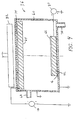
Referring now to Figure 1, a schematic diagram of a substrate having a patterned
dielectric layer 12 formed thereon is shown. The dielectric layer 12 has a via 14 having a
high aspect ratio, i.e, a high ratio of via depth to via width, of about three (3), but the
present invention may be beneficial in cooperation with vias having any aspect ratio. A
thin titanium layer 16 is deposited directly onto the substrate covering substantially all
surfaces of the dielectric layer 12 including the walls 18 and floor 20 of via 14. The thin
titanium layer 16 will generally have a thickness of between about 5 Å and about 700 Å,
with the preferred thickness being in the range between about 100 Å and about 200 Å. A
conformal PVD Al layer 22 is deposited on the titanium layer 16 to a desired thickness not
to exceed the thickness which would seal the top of the contact or via. The conformal PVD
Al layer 22 may be deposited in a sputtering chamber that holds a substrate at a distance of
at least about 100 mm from an Al target.
-
Referring now to Figure 2, the via 14 is filled with Al by reflowing a bulk PVD Al
layer 23 deposited on the conformal PVD Al layer (layer 22 of Figure 1). An integrated
PVD Al layer 24 will result from integrating the bulk PVD Al layer 23 that is deposited
onto the conformal PVD Al layer 22. The bulk PVD Al may contain certain dopants, and
upon deposition the bulk PVD Al layer 23 may integrate with the conformal PVD Al layer
22 so that the dopant is dispersed throughout much of the integrated PVD Al layer 24. In
general, the integrated PVD Al layer 24 does not need to be doped. The top surface 26 of
the integrated PVD Al layer 24 is substantially planarized. Because the titanium layer 16
provides good wetting of the conformal PVD Al layer 22, the dielectric layer or substrate
temperature during deposition of PVD Al may be from about room temperature to about
500°C.
The Apparatus
-
The metal deposition process of the present invention is preferably carried out in a
multichamber processing apparatus or cluster tool having a PVD chamber capable of
being operated at a pressure below about 0.35 milliTorr. A schematic of a multichamber
processing apparatus 35 suitable for performing the processes of the present invention is
illustrated in Figure 3. The basic apparatus is an "ENDURA" system commercially
available from Applied Materials, Inc., Santa Clara, California. A similar staged-vacuum
wafer processing system is disclosed in United States Patent No. 5,186,718, entitled
Staged-Vacuum Wafer Processing System and Method, Tepman et al., issued on February
16, 1993, which is hereby incorporated herein by reference. The particular embodiment of
the apparatus 35 shown herein is suitable for processing planar substrates, such as
semiconductor substrates, and is provided to illustrate the invention, and should not be
used to limit the scope of the invention. The apparatus 35 typically comprises a cluster of
interconnected process chambers including at least one long throw PVD metal chamber.
For the present invention, the apparatus 35 preferably includes a PVD Al chamber 36
having a substrate to target spacing of at least 100 mm for depositing conformal PVD Al
layers, and two additional PVD Al chambers 38 for depositing and reflowing PVD Al
layers. The apparatus 35 may further comprise a PVD Ti chamber 40 or another
barrier/wetting layer chamber, two pre-clean chambers 42 for removing contaminants
(such as PreClean II chambers available from Applied Materials), two degas chambers 44,
and two load lock chambers 46. The apparatus 35 has two transfer chambers 48, 50
containing transfer robots 49, 51, and two cooldown chambers 52 separating the transfer
chambers 48, 50. The apparatus 35 is automated by programming a microprocessor
controller 54 as described in more detail below. However, the process could also be
operated by individual chambers, or a combination of the above.
The PVD Chambers
-
Referring to Figure 4, a preferred long throw PVD chamber 36 is shown in more
detail. A sputtering target 64 and a semiconductor substrate 66 are contained within a
grounded enclosure wall 60, which may be a chamber wall as shown or a grounded shield.
The target 64 and the substrate are separated by a long throw distance of at least about 100
mm, preferably from about 150 mm to about 190 mm. The long throw chamber may also
contain a collimator (not shown) between the target 64 and the substrate 66 if needed to
provide a more uniform and symmetrical flux of deposition material to each location on
the substrate 66. Collimators that may be used in the PVD chamber are described in
United States Patent Application No, 08/792,292, filed January 31, 1997, which
description is incorporated by reference herein.
-
Referring still to Figure 4, the chamber 36 generally includes at least one gas inlet
68 connected to a gas source (not shown) and an exhaust outlet 70 connected to an exhaust
pump (not shown). A substrate support pedestal 72 is disposed at one end of the enclosure
wall 60, and the sputtering target 64 is mounted to the other end of the enclosure wall 60.
The target 64 is electrically isolated from the enclosure wall 60 by an insulator 74 so that a
negative voltage may be applied and maintained on the target with respect to the grounded
enclosure wall 60. The substrate support pedestal 72 is also electrically isolated from the
enclosure wall 60 by an insulator 76, so that a positive voltage may be applied and
maintained on the substrate and/or the support pedestal 72 with respect to the grounded
enclosure wall 60. In operation, the substrate 66 is positioned on the support pedestal 72
and a plasma is generated in the chamber 36.
-
During the deposition process of the conformal PVD metal layer according to the
present invention, a process gas comprising a non-reactive species such as Ar, is charged
into the PVD chamber 36 through the gas inlet 68 at a selected flow rate regulated by a
mass flow controller (not shown). The chamber pressure is controlled by varying the rate
that process gases are pumped through the exhaust outlet 70 and is maintained below
about 1 milliTorr to promote deposition of conformal PVD metal layers, preferably from
about 0.2 milliTorr to about 0.5 milliTorr.
-
A power source, such as a D.C. power supply 78, applies a negative voltage to the
target 64 with respect to the enclosure wall 60 so as to excite the gas into a plasma state.
Ions from the plasma bombard the target 64 and sputter atoms and larger particles of target
material from the target 64. The particles sputtered from the target 64 travel along linear
trajectories from the target 64, and a portion of the particles collide with, and deposit on,
the substrate 66.
-
A conventional magnetron sputtering source employs a rotating magnet 82 above
the target 64 to trap electrons adjacent the target and thereby increase the concentration of
plasma ions adjacent to the sputtering surface of the target 66. Rotation of the magnetron
82 during sputtering of the target 64 results in a radially symmetric target erosion profile.
-
Figure 5 is a schematic cross-sectional view of a PVD chamber 38 suitable for
performing a PVD processes of the present invention. The chamber 38 generally includes
a grounded enclosure wall 84, having at least one gas inlet 86 and an exhaust outlet 88
connected to an exhaust pump (not shown). A PVD target 89 is isolated from the
grounded enclosure wall 84 by an insulator 90. The PVD target 89 provides a sputtering
surface 92 for depositing material on a substrate 93 positioned on a support member, such
as a moveable pedestal 94. The pedestal 94 includes a generally planar surface 95 having
positioning pins 96 for receiving the substrate 93 thereon. A negative voltage may be
maintained on the target 89 with respect to the grounded enclosure wall 84 by a DC power
source 95.
-
A lift pin mechanism 97 raises and lowers the substrate 93 with respect to the
pedestal 94 while the pedestal is in a retracted position. The pedestal 94 extends to place
the substrate 93 adjacent the target during deposition of metal layers such as aluminum.
The pedestal 94 can be heated or cooled to control the substrate temperature.
Control Systems
-
Referring to Figure 6, the processes of the present invention can be implemented
using a computer program product 141 that runs on a conventional computer system
comprising a central processor unit (CPU) interconnected to a memory system with
peripheral control components, such as for example a 68400 microprocessor,
commercially available from Synenergy Microsystems, California. The computer
program code can be written in any conventional computer readable programming
language such as for example 68000 assembly language, C, C++, or Pascal. Suitable
program code is entered into a single file, or multiple files, using a conventional text
editor, and stored or embodied in a computer usable medium, such as a memory system of
the computer. If the entered code text is in a high level language, the code is compiled,
and the resultant compiler code is then linked with an object code of precompiled
windows library routines. To execute the linked compiled object code, the system user
invokes the object code, causing the computer system to load the code in memory, from
which the CPU reads and executes the code to perform the tasks identified in the program.
-
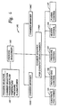
Figure 6 shows an illustrative block diagram of the hierarchical control structure of
the computer program 141. A user enters a process set and process chamber number into a
process selector subroutine 142. The process sets are predetermined sets of process
parameters necessary to carry out specified processes in a specific process chamber, and
are identified by predefined set numbers. The process parameters relate to process
conditions such as, for example, process gas composition and flow rates, temperature,
pressure, plasma conditions such as cooling gas pressure, and chamber wall temperature.
-
A process sequencer subroutine 143 comprises program code for accepting the
identified process chamber and set of process parameters from the process selector
subroutine 142, and for controlling operation of the various process chambers. Multiple
users can enter process set numbers and process chamber numbers, or a user can enter
multiple process set numbers and process chamber numbers, so the sequencer subroutine
143 operates to schedule the selected processes in the desired sequence. Preferably the
sequencer subroutine 143 includes a program code to perform the steps of (i) monitoring
the operation of the process chambers to determine if the chambers are being used, (ii)
determining what processes are being carried out in the chambers being used, and (iii)
executing the desired process based on availability of a process chamber and type of
process to be carried out. Conventional methods of monitoring the process chambers can
be used, such as polling. When scheduling which process is to be executed, the sequencer
subroutine 143 can be designed to take into consideration the present condition of the
process chamber being used in comparison with the desired process conditions for a
selected process, or the "age" of each particular user entered request, or any other relevant
factor a system programmer desires to include for determining scheduling priorities.
-
Once the sequencer subroutine 143 determines which process chamber and process
set combination is going to be executed next, the sequencer subroutine 143 causes
execution of the process set by passing the particular process set parameters to the
chamber manager subroutines 144A-C which control multiple processing tasks in different
process chambers according to the process set determined by the sequencer subroutine
143. For example, the chamber manager subroutine 144A comprises program code for
controlling CVD process operations, within the described process chamber 36 of Figure 4.
The chamber manager subroutine 144 also controls execution of various chamber
component subroutines or program code modules, which control operation of the chamber
components necessary to carry out the selected process set. Examples of chamber
component subroutines are substrate positioning subroutine 145, process gas control
subroutine 146, pressure control subroutine 147, heater control subroutine 148, and plasma
control subroutine 149.
-
In operation, the chamber manager subroutine 144A selectively schedules or calls
the process component subroutines in accordance within the particular process set being
executed. The chamber manager subroutine 144A schedules the process component
subroutines similarly to how the sequencer subroutine 143 schedules which process
chamber 36 and process set is to be executed next. Typically, the chamber manager
subroutine 144A includes steps of monitoring the various chamber components,
determining which components needs to be operated based on the process parameters for
the process set to be executed, and causing execution of a chamber component subroutine
responsive to the monitoring and determining steps.
Example 1
-
The apparatus of Figure 3 was used to fill apertures on the surface of a
semiconductor substrate. The apertures were precleaned to remove about 400 Å of
material including any oxides or other contaminants and then transferred to a PVD Ti
chamber for deposition of about 400 Å of a conformal titanium layer. The substrate was
then transferred to a PVD chamber 36 wherein the target to substrate distance is greater
than 150 mm for deposition of a conformal aluminum layer of about 4000 Å at a chamber
pressure of about 0.35 milliTorr. Deposition of aluminum commenced at room
temperature. The substrate was then transferred to an additional PVD Al chamber 38 for
deposition of about 4000 Å of bulk aluminum at less than 350°C with power input
exceeding 10 kW at a target to substrate spacing of less than 100 mm. The aluminum
layers (conformal and bulk) were then heated in the additional chamber 38 for reflow of
aluminum to fill the apertures. The temperature of the substrate during reflow was
maintained below 500°C. The surface of the aluminum after reflow was free of channels
and the apertures were free of voids. The aluminum surface had excellent reflectivity and
uniformity.
Example 2 (Comparison)
-
The apparatus of Figure 3 was used to fill apertures on the surface of a
semiconductor substrate for comparison to Example 1. The apertures were precleaned to
remove about 400 Å of material including any oxides or other contaminants and then
transferred to a PVD Ti chamber for deposition of about 400 Å of a conformal titanium
layer. The substrate was then transferred to PVD chamber 36 having a target to substrate
distance greater than 100 mm for deposition of an aluminum layer having a blanket
thickness of about 8000 Å. The aluminum layer was deposited at a chamber pressure of
about 0.35 milliTorr and was not conformal. The aluminum layer was then heated in the
chamber 36 to reflow the aluminum and fill the apertures. The temperature of the substrate
during reflow was maintained below 500°C. The surface of the aluminum after reflow
included small grooves although the apertures were free of voids. The aluminum surface
had similar reflectivity and reduced uniformity in comparison to the aluminum surface of
Example 1.
-
The process of the present invention provides excellent step coverage for filling
high aspect ratio apertures with a conformal layer of metal deposited by PVD at a pressure
less than about 1 milliTorr, preferably less than about 0.35 milliTorr, and a metal layer
deposited by PVD to fill the apertures. The deposited metal layers produce a uniform
surface having reduced surface trenching.
-
While the foregoing is directed to embodiments of the present invention, other and
further embodiments of the invention may be devised without departing from the basic
scope thereof. The scope of the invention is determined by the claims that follow.