EP1057117B1 - PROCEDE POUR LA MISE EN ANTEMEMOIRE HIERARCHIQUE DE DONNEES DE CONFIGURATION DE PROCESSEURS DE FLUX DE DONNEES ET DE MODULES AVEC UNE STRUCTURE DE CELLULE PROGRAMMABLE BI- OU MUTLIDIMENSIONNELLE (FPGAs, DPGAs OU ANALOGUE) - Google Patents
PROCEDE POUR LA MISE EN ANTEMEMOIRE HIERARCHIQUE DE DONNEES DE CONFIGURATION DE PROCESSEURS DE FLUX DE DONNEES ET DE MODULES AVEC UNE STRUCTURE DE CELLULE PROGRAMMABLE BI- OU MUTLIDIMENSIONNELLE (FPGAs, DPGAs OU ANALOGUE) Download PDFInfo
- Publication number
- EP1057117B1 EP1057117B1 EP99913087A EP99913087A EP1057117B1 EP 1057117 B1 EP1057117 B1 EP 1057117B1 EP 99913087 A EP99913087 A EP 99913087A EP 99913087 A EP99913087 A EP 99913087A EP 1057117 B1 EP1057117 B1 EP 1057117B1
- Authority
- EP
- European Patent Office
- Prior art keywords
- command
- trigger
- filmo
- die
- der
- Prior art date
- Legal status (The legal status is an assumption and is not a legal conclusion. Google has not performed a legal analysis and makes no representation as to the accuracy of the status listed.)
- Expired - Lifetime
Links
- 238000000034 method Methods 0.000 title claims abstract description 82
- 230000008569 process Effects 0.000 claims description 28
- 230000009471 action Effects 0.000 claims description 4
- 101000931570 Dictyostelium discoideum Farnesyl diphosphate synthase Proteins 0.000 claims 1
- 238000012545 processing Methods 0.000 abstract description 25
- 239000013598 vector Substances 0.000 description 39
- 230000006870 function Effects 0.000 description 14
- 241001136792 Alle Species 0.000 description 12
- 239000003999 initiator Substances 0.000 description 12
- 238000004891 communication Methods 0.000 description 11
- 238000013519 translation Methods 0.000 description 10
- 230000008901 benefit Effects 0.000 description 8
- 230000008859 change Effects 0.000 description 7
- 241001522296 Erithacus rubecula Species 0.000 description 5
- 238000007726 management method Methods 0.000 description 5
- 239000011159 matrix material Substances 0.000 description 5
- 230000002093 peripheral effect Effects 0.000 description 5
- 238000012546 transfer Methods 0.000 description 4
- 238000012217 deletion Methods 0.000 description 3
- 230000037430 deletion Effects 0.000 description 3
- 230000000694 effects Effects 0.000 description 3
- 238000005516 engineering process Methods 0.000 description 3
- 238000011156 evaluation Methods 0.000 description 3
- 238000013467 fragmentation Methods 0.000 description 3
- 238000006062 fragmentation reaction Methods 0.000 description 3
- 230000000712 assembly Effects 0.000 description 2
- 238000000429 assembly Methods 0.000 description 2
- 238000004364 calculation method Methods 0.000 description 2
- 238000005352 clarification Methods 0.000 description 2
- 230000001419 dependent effect Effects 0.000 description 2
- 230000005283 ground state Effects 0.000 description 2
- 238000009434 installation Methods 0.000 description 2
- 230000007246 mechanism Effects 0.000 description 2
- 230000006855 networking Effects 0.000 description 2
- 238000012913 prioritisation Methods 0.000 description 2
- 230000000717 retained effect Effects 0.000 description 2
- 238000012360 testing method Methods 0.000 description 2
- 101000936513 Loxosceles boneti Dermonecrotic toxin LbSicTox-betaIA1a Proteins 0.000 description 1
- 206010000210 abortion Diseases 0.000 description 1
- 230000004913 activation Effects 0.000 description 1
- 238000003491 array Methods 0.000 description 1
- 238000007630 basic procedure Methods 0.000 description 1
- 230000006399 behavior Effects 0.000 description 1
- 230000000903 blocking effect Effects 0.000 description 1
- 239000000872 buffer Substances 0.000 description 1
- 230000015556 catabolic process Effects 0.000 description 1
- 230000001427 coherent effect Effects 0.000 description 1
- 238000012790 confirmation Methods 0.000 description 1
- 238000010276 construction Methods 0.000 description 1
- 230000003247 decreasing effect Effects 0.000 description 1
- 230000003111 delayed effect Effects 0.000 description 1
- 238000010586 diagram Methods 0.000 description 1
- 230000006872 improvement Effects 0.000 description 1
- 230000000977 initiatory effect Effects 0.000 description 1
- 238000012544 monitoring process Methods 0.000 description 1
- 230000004044 response Effects 0.000 description 1
- 230000001360 synchronised effect Effects 0.000 description 1
- 230000009625 temporal interaction Effects 0.000 description 1
- 230000007704 transition Effects 0.000 description 1
- VLCQZHSMCYCDJL-UHFFFAOYSA-N tribenuron methyl Chemical compound COC(=O)C1=CC=CC=C1S(=O)(=O)NC(=O)N(C)C1=NC(C)=NC(OC)=N1 VLCQZHSMCYCDJL-UHFFFAOYSA-N 0.000 description 1
- 230000001960 triggered effect Effects 0.000 description 1
- 238000011144 upstream manufacturing Methods 0.000 description 1
- 239000011800 void material Substances 0.000 description 1
Images


Classifications
-
- G—PHYSICS
- G06—COMPUTING; CALCULATING OR COUNTING
- G06F—ELECTRIC DIGITAL DATA PROCESSING
- G06F15/00—Digital computers in general; Data processing equipment in general
- G06F15/76—Architectures of general purpose stored program computers
- G06F15/78—Architectures of general purpose stored program computers comprising a single central processing unit
- G06F15/7867—Architectures of general purpose stored program computers comprising a single central processing unit with reconfigurable architecture
-
- G—PHYSICS
- G06—COMPUTING; CALCULATING OR COUNTING
- G06F—ELECTRIC DIGITAL DATA PROCESSING
- G06F12/00—Accessing, addressing or allocating within memory systems or architectures
- G06F12/02—Addressing or allocation; Relocation
- G06F12/08—Addressing or allocation; Relocation in hierarchically structured memory systems, e.g. virtual memory systems
- G06F12/0802—Addressing of a memory level in which the access to the desired data or data block requires associative addressing means, e.g. caches
- G06F12/0806—Multiuser, multiprocessor or multiprocessing cache systems
- G06F12/0811—Multiuser, multiprocessor or multiprocessing cache systems with multilevel cache hierarchies
-
- G—PHYSICS
- G06—COMPUTING; CALCULATING OR COUNTING
- G06F—ELECTRIC DIGITAL DATA PROCESSING
- G06F12/00—Accessing, addressing or allocating within memory systems or architectures
- G06F12/02—Addressing or allocation; Relocation
- G06F12/08—Addressing or allocation; Relocation in hierarchically structured memory systems, e.g. virtual memory systems
- G06F12/0802—Addressing of a memory level in which the access to the desired data or data block requires associative addressing means, e.g. caches
- G06F12/0806—Multiuser, multiprocessor or multiprocessing cache systems
- G06F12/0813—Multiuser, multiprocessor or multiprocessing cache systems with a network or matrix configuration
-
- G—PHYSICS
- G06—COMPUTING; CALCULATING OR COUNTING
- G06F—ELECTRIC DIGITAL DATA PROCESSING
- G06F12/00—Accessing, addressing or allocating within memory systems or architectures
- G06F12/02—Addressing or allocation; Relocation
- G06F12/08—Addressing or allocation; Relocation in hierarchically structured memory systems, e.g. virtual memory systems
- G06F12/0802—Addressing of a memory level in which the access to the desired data or data block requires associative addressing means, e.g. caches
- G06F12/0806—Multiuser, multiprocessor or multiprocessing cache systems
- G06F12/084—Multiuser, multiprocessor or multiprocessing cache systems with a shared cache
Definitions
- a central and global unit which controls the reconfiguration of parts (e.g. cells (CELs)) of one or more components, creates bottlenecks when many different reconfiguration requests have to be handled at once.
- CELs cells
- Such a central unit severely limits the advantages of the parallelism of the modules described, since it represents the typical "bottleneck" and thus considerably slows down the processing of the data.
- the assignment of the event source to the configuration to be loaded is problematic since absolute addresses of the configuration memory are used.
- the reconfiguration unit must therefore contain a type of memory management system which, similar to an operating system, also logs which memory areas are used by which configuration.
- An additional problem is the management of resources (for example, CELs). It must be ensured that each CEL is only assigned once to an algorithm started by a reconfiguration request, and that to the one that also uses the other surrounding CELs, since otherwise deadlocks can occur ,
- a matrix of CELs is unconfigured and in the RESET state. Each CEL is able to indicate whether it is in a reconfigurable state. All CELs in the matrix are ready to be configured; are therefore in a reconfigurable state.
- a first configuration routine (KR1) is loaded, the matrix not being fully used. The configured CELs override the indication that they are in a configurable state.
- a second configuration routine (KR2) that is independent of the first is loaded into a group of the CELs that have not yet been configured.
- KR3 second configuration routine
- KR3 must be stopped until the required CELs have been released, ie KR1 and KR2 have terminated.
- KR4 a load request is added for a fourth configuration routine (KR4) and a fifth configuration routine (KR5), all of which cannot be loaded immediately since they use CELs used by KR1 and KR2.
- KR3 and KR4 partly use the same CELs, KR5 does not use any of the KR3 and KR4 CELs.
- the basic object of the present invention is a unit - hereinafter called configuration table (CT) - which is hierarchically structured and can occur several times at each level, the number of CTs decreasing from the lowest hierarchical level to the highest so that at the highest level there is exactly one CT.
- Each CT configures and controls a number of configurable elements (CELs) independently and in parallel.
- CTs at higher hierarchy levels can cache configuration routines for lower-level CTs. If several of the lower-lying CTs require the same configuration routine, this is temporarily stored in the case of a higher-lying CT and called up by the individual CTs, the higher-lying CT calling up the relevant configuration routine only once from a global common configuration memory, which achieves a cache effect.
- the present invention can be used as a cache method for instruction and data caching in microprocessors, DFP or the like with multiple arithmetic units.
- some of the units described below can be omitted (e.g. FILMO), but the hierarchical structure does not change fundamentally. Therefore, this use is considered a subset and will not be discussed further.
- a significant advantage of the described method compared to conventional cache methods is that data and / or code are cached selectively, ie using methods that are precisely matched to the algorithm.
- the present invention also enables the completely deadlock-free reconfiguration of large cell structures.
- a kind of cache of the configuration data is achieved through the tree structure of the configuration units. Configurations are mainly accessed locally. In the worst case, a configuration must be loaded from the higher-level configuration memory if the data in question is not present in any of the hierarchically arranged CTs. Deadlocks are prevented by introducing a fixed chronological sequence of the configurations to be loaded and by combining the configurations into a list. The status information of the CEL is saved before loading and therefore remains unchanged while the entire list of configurations is being processed.
- a configuration table is an active unit, based on synchronization signals, so-called triggers, responding.
- the triggers are of a two or multi-dimensional matrix of electronic assemblies, usually arithmetic or logical units, Address generators, computing units, etc. - hereinafter called configurable elements (CEL) - generated.
- CEL configurable elements
- This task does a CT by doing a variety of possible ones Configuration routines (KR), which in turn each consist of a plurality of individual configuration words (KW) exist, managed and based on a number of CELs trigger conditions with one or more of the KR configure.
- KR Configuration routines
- a CEL receives one or each several of the configuration words that match the address of the are configured to be configured.
- a KR must do so completely and correctly on a plurality of CELs are mapped, with several CELs in groups can be summarized; the with each different but fully executed KRs can be configured. All CELs are in one Group interconnected so that after finding a necessary reconfiguration through all grouped CELs a common signal (ReConfig) is communicated that each CEL to finish data processing and into one reconfigurable state.
- ReConfig common signal
- a trigger signal is sent to a CT Posted.
- This CT detects the trigger source and selects one to be loaded from a look-up table Configuration (KR).
- KR look-up table Configuration
- the incoming trigger signals are blocked, there are no further triggers until for complete processing of the current configuration accepted.
- a configuration consists of several Instructions that are transmitted to a set of CELs. In a system that is configurable at runtime however, it does not ensure that everyone Configuration command (KW) can also be executed. This can fail, for example, because the addressed configurable element (CEL) its task has not yet ended and therefore no new ones Can accept configuration data.
- CT goes back to the state in which they accepted trigger signals to possibly continue Load configurations.
- the works in this state CT the FILMO at regular intervals, by a Timer controlled, from.
- the configurations to be loaded are prioritized by the CT running through the FILMO memory before the configuration to be loaded is processed.
- a FIFO-like structure of FILMO ensures that KWs that could not be fully processed during previous trigger requests automatically receive a higher priority than the new WK to be processed.
- the actual configuration activated by the occurrence of the trigger signal is then processed.
- the structure of the FILMO corresponds to the FIFO principle, which means that the oldest entries are processed first.
- the FILMO is controlled by a timer at regular intervals.
- the remaining configurable items not involved (CEL) continues to work in parallel during this phase is not affected in their function. This can the case occur that during the CT the FILMO processes one or more configurable elements (CELs) change to the "reconfigurable" state. There the CT is working on any Location within the FILMOs could be the following case occur:
- the CT tries to process a first command addressed configuration element (CEL) is not in the state "reconfigurable”.
- the CT drives thus continue with the next command (KW).
- KW next command
- the CT processes a second configuration command (KW), which is the same configurable element (CEL) used like the first configuration command, however comes from a different configuration.
- KW the same configurable element used like the first configuration command
- Configuration A and configuration B should be configured.
- the CT has already loaded the hatched part of configuration A and configuration B.
- Configuration A still requires the light-double hatched area of configuration B to complete
- configuration B still requires the dark-double hatched area of configuration A to complete. Since both configurations have not yet been completely completed and are therefore not functional, neither of the two configurations the termination state in which one of the two configurations would be removed. Both configurations are waiting for the configurable elements that are still required to be released.
- a deadlock prevented by the CT before processing the FILMO the states of all configurable elements are recorded and thereafter no changes until the end of the process allows more or ignores changes that occur. With in other words, it will either be the states of all configurable elements before processing the FILMO secured or a change in conditions during the Processing of the FILMO prevented.
- a possible technical implementation is the use of a register in any configurable item in which the state before Processing of the FILMO is secured.
- the CT works only on the basis of the recorded states and not with the current states of the configurable elements. This ensures that everyone to be processed Command (KW) the same state of configurable Elements (CELs). This step does not close out that one or more configurable items in the state during the processing of the FILMO skip "reconfigurable". This change is for the CT just not immediately during processing visible, but only at the beginning of the next Run.
- CTs become one Hierarchy interconnected in a tree structure.
- a bus system is located at the individual nodes (CTs) (Inter-CT bus) that each have an upper node (CTs) connects to multiple lower nodes (CTs).
- CTs upper nodes
- CTs lower nodes
- the upper nodes then send the data to the lower nodes. Swap the lower nodes status information among themselves, for this the Networks used between the higher nodes that must resolve the addresses accordingly.
- CT hierarchies are arranged so that for addressing a binary tree can be used for the individual CTs. This means that the least significant address bit is the features individual leaves of the tree and each additional address bits one hierarchy level higher selected. Each CT thus has a unique one Address.
- the structure of the binary tree can be one-dimensional or be done multidimensionally by one per dimension Binary tree is built.
- a specific CT (TARGET) is addressed by the initiating CT (INITIATOR) either the exact Specifies destination address, or TARGET addressed relatively.
- Bit15 is set if the CT of the next higher hierarchy level is to be selected. Bit14 identifies broadcasts, ie selects all CTs. The X / Y addresses indicate the address of TARGET based on the address of INITIATOR.
- the addresses are signed integers.
- TARGET is determined by adding the Y / X addresses of the address field to the current address position. Each level has a certain address width. The adders correspond to this width.
- An overflow or underflow in the addition means that the addressed CT is not below the current node and the address request is forwarded to the CT above it (the next higher node). If there is no overflow or underflow, TARGET is located below the current node.
- the address bit calculated at the current level selects the CT located directly below the current node. From this, the next lower CT (node) is selected based on the correspondingly calculated address bit.
- the access to the Inter-CT bus is from one Arbiter manages. All lower nodes are the same prioritized. The upper node has a higher one Priority. This causes accesses from a higher level Nodes are transferred down, or already one others have traveled a long way from the INITIATOR Think about access.
- CT control state machine
- KRs configuration routines
- GC garbage collector
- FILMO FILMO
- the memory is an ordinary random access memory designed, all technically possible Implementations can and will be used for local storage of KRs for the respective CT and used their subordinate CTs.
- the memory also as ROM, EPROM, EEPROM, Flash-ROM etc. be designed to the block with a fixed, ASIC or PLD-like (see status of Technology) function.
- KW are sent to the via an output interface (OUT) associated CELs passed.
- OUT output interface
- Acknowledge the CELs (ACCEPT) provided they are in a reconfigurable Condition are the receipt of the KW.
- REJECT a KW acknowledged
- FILMO FIFO-like Memory
- the CTS receives a request to process a KR through trigger signals.
- the trigger signals pass through a mask, which is a filter that filters out (unwrapped) triggers.
- a mask can be constructed by AND gates (AND), which ANDs a trigger with an enable signal.
- the triggers are converted into binary signals via a prioritized round robin arbiter (SCRR-ARB).
- SCRR-ARB prioritized round robin arbiter
- a prioritized round robin arbiter combines the advantage of equal rights for a round robin arbiter with the recognition of the next release in one cycle, that is, the advantage of a priority arbiter.
- the masked triggers are switched as addresses to a first lookup table (LUT1), which is a memory that assigns the ID of the relevant KR to the trigger that is received as the address and outputs it on the data lines.
- LUT1 a first lookup table
- LUT2 the ID of the KR is assigned to the address of the memory location of the KR in the CTR.
- the second lookup table is not only used to assign trigger signals, rather commands that use an ID as parameters also use LUT2 to assign addresses.
- the assignment of the trigger signals to the relevant IDs is entered in the LUT1 using the "REFERENCE" command described below.
- the administration of the LUT2, i.e. the assignment of the IDs to the addresses in the CTR is done automatically by the CTS and the GC.
- This command is only valid at the first address of the CTR.
- the complete boot KR is first written to the CTR, but not the start sequence of the boot KR BEGIN ⁇ 0>.
- WAIT-FOR-BOOT which is set automatically on a RESET.
- WAIT_FOR_BOOT is only overwritten with BEGIN ⁇ 0> after the entire boot KR has been written to the CTR and the CTS begins to process the boot KR.
- WAIT_FOR_BOOT must not occur within a program.
- BOOT ⁇ CT-ID> indicates in which CT the subsequent boot KR should be written. After BOOT ⁇ CT-ID> there is no BEGIN, the boot KR is not completed by STOP, but by a subsequent BOOT ⁇ CT-ID>. A STOP ends the boot process. BOOT ⁇ CT-ID> must not occur within a program.
- the ID of the requested KR is given to the LUT2 as an address.
- the LUT2 checks whether a valid address exists in the CTR. If this does not exist, ie ⁇ ID> points to 0 in LUT2, load ⁇ ID> is sent to the CTS.
- the CTS requests the KR concerned from the hierarchically superior CT.
- the higher-level CT achieves this requirement in the form of a trigger and is evaluated accordingly.
- the higher-level CT sends the requested KR to the requesting CT.
- the data is written into the CTR starting from the address pointed to by the FREE POINTER (FP), the FP being increased by one after each write access.
- the garbage collector (GC) is called to remove the lowest KR within the CTR and compress the CTR.
- the FP is reset. This process continues until the KR to be loaded fits completely into the CTR.
- the KR with the ID ⁇ A> should be changed.
- the ID ⁇ A> is put together with the new address of the KR in the configuration memory from the parent unit (HOST) into one for it intended register of the ROOT-CT written.
- the ROOT-CT sends the command to all underlying CTs REMOVE ⁇ A>. Thereupon remove all CTs when reached a STOP or during IDLE cycles, i.e. as soon as none KR is executed, the KR related to this ID from the CTR and set the LUT2 at address ⁇ A> to "NoAdr" that means there is no valid address entry for ID ⁇ A> in LUT2. If the ID ⁇ A> is requested again, the missing entry (“NoAdr”) forces in place of ⁇ A> the LUT2 each CT to request the KR ⁇ A> from the ECR again.
- the FILMO The FILMO
- a KR mainly consists of the PUSH command, the new configuration words to a specific address writes. Is the writing of a configuration word of type KW not possible, because the addressed configurable item (CEL) is not ready a new one Receive configuration (REJECT), that will Configuration word instead of the addressed configurable element (CEL) in a memory, in called the following FILMO.
- the following Commands are processed normally until on again Configuration word cannot be written then written into the FILMO.
- the configuration words (KW) that could not be written by the CTS to the addressed elements (CELs) are appended to the FILMO again, ie the KW are written to the end (from the reading direction) of the FILMO. If the FILMO is full, ie there are no free entries for configuration words, the execution of the KR is stopped. The FILMO is run through until enough configuration words have been written and a corresponding number of free entries have been created, whereupon the KR is processed further.
- the FILMO is a FIFO-like memory that is always traversed linearly from the oldest entry, but unlike a FIFO, entries are skipped (First In Linear Multiple Out).
- CTS configuration table state machine
- the configuration table state machine controls the CT. It executes the commands of the KR and responds to incoming triggers. It takes over the management of the FILMO, ib reads it out in IDLE cycles and the FILMO before performing a KR. It reacts to the signals generated by the LUT structure illegally ⁇ TRG> (illegal trigger, see Fig. 1, 0102) and load ⁇ ID>. load ⁇ ID> is generated if there is a cache miss in LUT2 (0105) or the KR / IKR referenced by ID has been marked as deleted (0107). It reacts to the control signals from the higher-level CT. An implementation example for processing the commands is shown in FIGS. 2 to 7.
- Each CT has a connection to several trigger signals belonging to its respective hierarchy level, which are combined to form a bus.
- Incoming triggers are evaluated using a mask, ie only the activated trigger signals are forwarded.
- the activated trigger signals are temporarily stored in a sample register (sampled).
- An arbiter selects one of the stored trigger signals and converts the signal into a binary vector.
- the selected trigger signal is deleted from the sample register.
- the binary vector is forwarded to a first lookup table (LUT1), which translates the binary vector into the identification number (ID) of the configuration routine (KR) to be called.
- the ID is translated into the address of the KR in the CT memory (CTR) in a second lookup table (LUT2).
- the CT state machine sets its program pointer (PP) to this address and starts executing the KR.
- the "trigger vector" command represents a binary value that references an entry in the LUT2 of the receiving CT.
- the sending of trigger vectors is necessary, for example, to start a KR in a further CT within an ICR, for example to control the peripherals or the memory.
- Trigger vectors To start a KR in a foreign CT via Trigger vectors must be used to achieve freedom from deadlocks a synchronization process can be created. The procedure must take into account that only one KR within a certain group of CTs further KR on others CTs within this group will start. Starting several KR at the same time can result in a deadlock between the CTs perform, similar to the deadlock already described the CEL level.
- Inter-CT bus Inter-CT bus
- This bus system connects all the CTs in the group and a CT directly superior to the group.
- the bus system is arbitrated by a CT using the GETBUS command, which is functionally similar to GETCTS.
- the commands are forwarded to the CTs of the same group via the bus system. If the addressed CT # is not within the group, the higher-level CT automatically arbitrates its higher-level bus and the command is forwarded.
- the arbitrated buses remain assigned to INITIATOR and are therefore blocked for all other CTs until either a rejection occurs or the LOOSEBUS command resolves the bus.
- LOOSEBUS is comparable to LOOSECTS.
- the GO signal is sent to all participating Cts. This is done either with the LOOSEBUS command or a special upstream command.
- Commands, ib triggers are also processed according to the basic procedure already described. A rejection occurs if a bus system cannot be arbitrated.
- the CTs of a level have the same priority, the higher-level CT has a higher priority.
- the command remains active until the addressed CT accepts the command (ACCEPT) or rejects it (REJECT).
- a register is assigned to the decoder the decoded values (ARB-DEC) of the decoder at the TF1 inverse clock edge (TF2) takes over.
- ARB-DEC will coupled back to the mask (ARB-MASK) and switches the individual input signals (ARB-IN) are free.
- ARB-REG can be provided with an enable input (EN), which only allows the register contents to be changed with TF2 if a corresponding signal is present.
- EN enable input
- a binary vector is not output for every cycle, but dependent on an activation by EN and TF2.
- the input is necessary for synchronization if the downstream circuit cannot process in one clock cycle, but requires several cycles and only then accepts the next binary vector.
- a CT can also be implemented in a microcontroller architecture. It is easy to see that the basic functions, such as trigger control, lookup tables LUT1 and LUT2, as well as the inter-CT communication and the writing of the KW to the CEL, can easily be carried out by a microcontroller. Only the construction of an efficient FILMO is a problem, which is particularly noticeable in the achievable performance. The structure of the FILMO is therefore dealt with separately.
- the FILMO is not designed as a separate memory. Rather, the usual program memory is expanded by the FILMO functionality. For this purpose, an additional bit (FILMO-BIT) is assigned to each KW, which indicates whether the corresponding KW has been written to the CEL or not. If FILMO-BIT is set, the corresponding KW is not carried out. The FILMO-BIT is reset when a Kws is written to the memory. All KRs within a CT are linked to one another via a linked list (FILMO-LIST) in the order in which they were called by trigger or LOAD ⁇ ID>. A KR remains in the FILMO-LIST until it has been completely executed, then it is removed from the list.
- FILMO-BIT linked list
- the FILMO-LIST is run in accordance with the FILMO process and thus represents a direct replacement for the FILMO memory. (For the sake of completeness, it should be noted that contrary to the original FILMO procedure, no KR can appear twice in the list. If a KR that is still in the FILMO-LIST is called, its execution must be delayed until it leaves FILMO -LIST was removed.)
- a garbage collector is used to remove KRs that are no longer required.
- the GC starts when either there is insufficient space to load a new KR in the memory and IDs have to be removed; or a KR is explicitly deleted by the REMOVE command - with the ID of the KR to be deleted.
- all KRs are linked to one another via a linked list.
- GC runs through the list and removes the KRs that are no longer required by overwriting them with other KRs and adjusting the list entries accordingly.
- the remaining KRs in the memory are shifted in such a way that the memory gap created by the KR to be deleted is closed and a larger contiguous free space is created at the end of the memory.
- Figure 1 shows the sequence of CTR address generation within a CT.
- An incoming binary trigger vector (0101) in LUT1 is translated to a valid KR or IKR ID. If there is no valid ID, an "Illegal Trigger" signal is generated (0102), which indicates that the trigger is not known in LUT1. The signal can be forwarded to the higher-level CT as an error message or ignored.
- the translation of "trigger" to "ID” is entered in the LUT1 using the "REFERENCE” command.
- a valid ID (0103) is forwarded to the LUT2. IDs that are specified within instructions, i.e. by an operand (0104), directly affect the LUT2.
- the LUT2 translates an incoming ID into the address of the KR / IKR within the CTR.
- the "Miss” signal is generated (0105). If the translated address of the KR / IKR is marked with the token "NoAdr”, "NoEntry” (0107) indicates that the address has been deleted. “Miss” and “NoEntry” indicate that a translation to an internal CTR address is not possible. On the basis of this signal, the LOAD state machine reloads the KR / IKR with the corresponding ID from an overlying CT. If a valid address is available, it is forwarded to the pointer arithmetic of the address generator (0106). In LUT1, an incoming binary trigger vector is either translated into an ID or a further trigger vector, in which case the trigger vector is output (0108).
- FIG. 2 shows the sequence when loading a KR / IKR.
- First the ID (0201) of the KR / IKR to be loaded is sent to the CT above.
- the value of the FreePointer (FP) is then entered in LUT2 at the location of the entry for the requested ID.
- FP points to the entry after the last entry in the CTR used for a KR / IKR. This is the first entry on which the KR / IKR to be loaded is saved.
- the state machine is waiting for a data word from the CT above. As soon as the word is available, it is written to the point referenced by FP. FP is incremented.
- FP points to an entry after the end of the CTR, the first entry in the CTR is removed to make room (0202); FP is updated. If the data word sent by the CT above it is "STOP", the loading process is interrupted (0203), otherwise it continues with waiting for a new data word (0204).
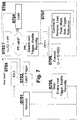
- the "MASK” command is shown in FIG. 3a .
- the operand of the command is written to the MASK register.
- the MASK register is located at the input of the trigger signals before LUT1 and masks out invalid triggers.
- the "TRIGGER” command sends the operand of the command as a trigger vector to the other CTs.
- the "REFERENCE” command writes the translation of a trigger for the corresponding KR / IKR ID into LUT1.
- the “WAIT” command is shown in FIG. 4a .
- the operand of the command is written to the WAITMASK register. All triggers except for the expected one and therefore activated in WAITMASK are ignored. The program flow is only returned after the trigger has occurred.
- the "PUSH” command is shown in FIG. 4b .
- the configuration word is sent to the addressed configurable element (CEL). Does the CEL not accept the configuration word; because the CEL is, for example, in the "not configurable”state; the configuration word is written to FILMO (0401).
- Figure 8 shows the structure of an SCRR-ARB.
- the signals to be arbitrated are sent to a mask (0801) via DataIn, which switches through or blocks a coherent part of the signals according to the known table.
- a conventional prior art priority arbiter (0802) arbitrates a signal from the set of switched through and provided its binary vector (BinaryOut) together with a valid / invalid identifier (ValidOut) (also according to the prior art) as the output of the SCRR ARB.
- This signal is decoded according to the known table (0803) and passed to a register for clock synchronization (0804).
- the DataIn mask is switched via this register.
- the register is controlled either by a clock or a Next signal (Enable EN), which queries the next valid binary vector.
- the register In the event of a reset or if the identifier (ValidOut) indicates invalid, the register is switched so that the DataIn mask switches through all signals.
- the structure of the mask is shown in 0805.
- the mask is shown again in 0806, the signals DataIn 0..DataIn 1 having the same priority according to the SCRR principle, while DataIn m .. DataIn n have higher priority.
- LUT1 In Figure 9, the LUT structure is depicted.
- the binary vector (BinaryIn) of the arbitrated trigger is led to the address input of LUT1 (0901).
- LUT1 either translates the binary vector into a valid trigger to forward it to another CT or a valid ID. Both are output via 0910.
- 0911 indicates whether it is a trigger or an ID. If no translation of the incoming binary vector is entered in LUT1 using the "REFERENCE” command, --- the signal "Illegal Trigger" 0914 is generated --- by means of a bit entry or a comparator on a specific token (eg "VOID").
- a trigger is sent to external CTs via 0912, IDs are processed via the multiplexer (0902).
- 0902 either switches the data output of LUT1, which indicates a valid ID, or the ID register (0903) of the CT to the address input of LUT2 (0904).
- 0904 has a cache-like structure, ie the low-order part (0906) of the data output from 0902 is switched to the address input from 0904, while the higher-order part (0907) is switched to the data input from 0904.
- the data output belonging to 0907 is compared with 0907 via a comparator (0905).
- the advantage of this method is that 0904 does not have to have the depth to translate all IDs, but can be considerably smaller. Similar to an ordinary cache, only a part of the IDs is translated, whereby it can be determined in the LUT2 using 0907 whether the selected ID corresponds to the one specified by LUT1. This corresponds to a cache / TAG method according to the prior art.
- the LUT1 is activated with the "REFERENCE” command Translation of the incoming binary vector to one Trigger or ID loaded.
- the operands of the instruction are routed to LUT1 via bus 0913. about the same bus is loaded with the ID register (0909).
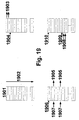
- the structure of a FILMO is shown in Figure 11 .
- the data passes from the CTR (1101) into the FILMO and is either written to the FILMO-RAM (1103) via the multiplexer (1102) or sent to the configurable elements (1116) via the multiplexer (1104). If data in 1103 is deleted, a "NOP" token is written after 1103 via 1102. The "NOP" token is recognized via the comparator (1105) at the data output and writing to the configurable elements is prevented. Either the write pointer WriteP (1107) or the read pointer (1108) is fed to the address input of 1103 via the multiplexer 1106. The read pointer is saved in register 1109 in order to enable a reset (see FIG. 6).
- the fill level counter Full (1110) of 1103 is stored in the register 1111 for resetting in accordance with FIG. 6.
- Two comparators test whether 1103 is empty (1112) or full (1113).
- the multiplexer 1115 is used to select whether the control signals of the state machine (from 1101) or the FILMO are sent to 1116.
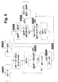
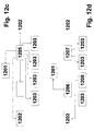
- FIG 12a shows the hierarchical structure of the CTs. All CTs obtain their data from the ROOT-CT (1201) and the ECR (1204) assigned to them. One or more CTs exist for each implementation level in a module. Each CT is responsible for managing its level and the underlying CTs. It is not necessary that all branches of the tree are of the same depth. For example, fewer levels can exist for controlling the periphery (1202) of a module than for controlling the working units (1203). The data transfer is tree-like. Each CT works as a cache for all CTs below it.
- Figure 12b shows the trigger flow between the CTs. While the data flow is tree-like, the trigger flow is not defined. Any CT can send a trigger to any other. Usually a trigger exchange takes place only from the sheets (1203) in the direction of the ROOT-CT (1201). Under certain circumstances, however, the transfer can also run in the opposite direction.
- a trigger vector broadcast is shown in FIG. 12c , 1205 sending a trigger vector to all CTs.
- Figure 12d shows a HIGHER trigger vector, the 1206 sends the CT above it. 1207 sends one LOWER trigger vector to all CTs below it. 1208 transmits a directly addressed (ADDRESSED) trigger vector to a specific CT that is not directly related 1207 is connected.
- ADRESSED directly addressed
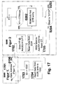
- FIG. 14 shows a LUT system modified compared to FIG. 9, which is used in ROOT-CTs and CTs of medium hierarchy levels.
- the basic difference to the CTs described so far is that ID and / or trigger vectors have to be managed by the CT instead of individual trigger signals.
- Each vector is assigned a handshake signal (RDY) to indicate the validity of the vector, which is sent to an arbiter (1401).
- RDY handshake signal
- Either one of the trigger vectors (1404) or one of the ID vectors (1405) is selected via the multiplexers (1402, 1403).
- Trigger vectors go directly to the address input of LUT1 (1406), which is otherwise connected according to FIG. 9.
- the ID register (1407) is also connected according to FIG. 9. In contrast to FIG.
- the multiplexer 1408 has three inputs (cf. 0902).
- the multiplexer is controlled by the arbiter 1401 in addition to the state machine. Via the additional input, ID vectors are forwarded directly to LUT2 via 1403. Bus 1409 is used for this.
- IDs according to FIG. 9 can also be switched directly to LUT2 using a multiplexer (1408). The IDs can then be sent directly from the CEL to LUT2 without translation.
- "Trigger / ID Out is generated according to FIG. 9. A "ValidIn” signal that is forwarded to a "Valid Out” according to FIG. 9 does not exist.
- a "Valid Trigger Out” for trigger vectors and a “Valid ID Out” for ID vectors are generated to instruct the state machine how the processing should take place.
- the bus 1409 is routed via 1410 to a further unit which only exists in the ROOT-CT and is described in FIG. 15.
- a ROOT-CT requires an interface to the external configuration memory (ECR), as well as the necessary address generator and units for managing access to the ECR.
- ECR external configuration memory
- a conventional CT translates incoming trigger vectors in LUT1 to an ID and in LUT2 the ID to a storage location in the CTR (see FIG. 16a ).
- a ROOT-CT When accessing the ECR, a ROOT-CT translates an ID within the ECR to an address in the ECR at which the KR / IKR referenced by ID begins.
- this memory area is located at the lower end of the ECR and is called LUT-ECR to underline the similarity to LUT2.
- the translation of a trigger to an ID takes place according to the already known CTs in LUT1 (1601).
- Figure 16b illustrates access to the ECR for better understanding.
- an ID reaches the multiplexer 1501 via the bus 1410 in FIG. 14.
- the ID is written into the loadable counter 1502 via 1501.
- the output of 1502 leads to the address bus (1504) of the ECR via a multiplexer 1503.
- the translation of the ID to a memory address is sent to 1501 via a multiplexer / demultiplexer (1506), which loads 1502 with the memory address.
- the data words of the corresponding KR / IKR are then read from the ECR and written into the CTR via the state machine LOAD-ECR (see FIG. 17), 1502 being increased after each read operation; until the "STOP" command has been read.
- the higher-level HOST writes via interface 1507 over 1503/1506 the KR / IKR into the ECR. It is about the state machine (CTS) arbitrates whether the HOST or the ROOT-CT has access to the ECR.
- CTS state machine
- BOOT-KR basic configuration
- BOOT-ADR fixed memory address
- Storage location 0h is recommended as BOOT-ADR, provided the IDs start with 1, otherwise 2 ID or any other storage location can be used. In the exemplary embodiment, 2 ID is used.
- the ROOT-CT leads to the loading of the BOOT-KR at the point BOOT-ADR performs a lookup if a BOOT-KR is loaded is.
- the ROOT-CT rewrites the data after 1502 there the BOOT-KR until a "STOP" command occurs to load.
- FIG. 17 shows the sequence in a ROOT-CT when loading a KR / IKR from the ECR. If an ID is not in the internal CTR (see FIG. 1, 1701), the ID is written in counter 1502 (1703). Access to the ECR with the address in 1502 provides the base address of the KR / IKR. This is written in 1502 (1704). A LOAD according to FIG. 2 takes place (1702). The data is read from the ECR instead of a higher-level CT (1705) and not only written to the own CTR, but sent to the lower-level CT (1706).
- FIG 19 illustrates the FILMO principle.
- FILMO (1901) is always read through from start to end (1902). If entries are written and deleted from the beginning of the FILMO (1903), the read pointer is moved to the first undeleted entry (1904). If entries are written from the middle of the FILMO (1905), the read pointer remains unchanged (1906), the entries are marked with "NOP" (1907). If data is written into FILMO (1908), it is appended to the end after the last entry (1909). The read pointer (1910) remains unchanged.
- CTs are similar to the ROOT-CT, which already has the LUT2 AND the CTR integrated in the ECR. For understanding the procedure is not a description of these CTs required.
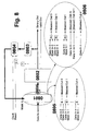
- the CT 2007 requests data from the overlying CT, which requests the data from the ROOT-CT 2004; the ID of the requesting KR / IKR (2001) is transferred with the data request.
- the data (2002) will be sent to 2007. All other, later accesses are rejected (2003).
- the data is written back (2005), other, later accesses are accepted again (2006).
- FIG. 20c data is requested from a CT middle hierarchy, is in possession of the data and sends it to 2007.
- the ID for locking the data is sent to all CTs in the hierarchy (2001).
- the data is written back (write-back) in FIG. 20d, the data are written to all CTs in the hierarchy and the ID is deleted.
- FIG. 21 shows the communication of an INITIATOR CT (2101) via several intermediate CTs (2104, 2105, 2106) with a TARGET CT (2102), as well as the direct communication without intermediate levels with a TARGET CT (2103) according to the GETCTS / LOOSECTS Method.
- 2101 establishes a connection to 2103. After successful installation, 2101 of 2103 receives a GRANT as confirmation of the installation. Then 2101 establishes the connection to 2102 via 2104, 2105, 2106. The connection to 2102 is only confirmed (GRANT) when 2102 is reached. If the connection cannot be established because one of the buses is busy, a REJECT is sent to 2101 and 2101 aborts the process.
- connection to 2103 is also broken and a REJECT is sent to 2103.
- 2101 sends a GO command to 2103 and 2102 in order to simultaneously confirm 2103 and 2102 that the bus has been successfully set up and synchronized.
- This protocol enables data or commands to be transmitted synchronously and deadlock-free, since GO ensures that all TARGETs receive the commands correctly.
- FIG. 22 shows the sequence of the inter-CT communication according to the GETBUS / LOOSEBUS method. While in the procedure 21, the respective higher-level CTs have the controlling and prioritizing task, control is taken over here by the inter-CT buses (2201). A connection to 2103 is established by the INITIATOR-CT (2101) requesting its local inter-CT bus (2202). Requests are confirmed if the bus is free (ACCEPT) or rejected if the bus is busy (REJECT). Then it sends the address of 2102 on the bus. According to the addressing scheme, the bus control recognizes that the address is outside the local bus addresses and establishes a connection to its local bus via the higher-order CT 2104 (2203).
- the overlying CT has a higher priority (2205). This prevents a very advanced bus structure that is already running over several levels from being interrupted by a still very local bus structure. With an extended protocol, in the case of a REJECT, it is only possible to dismantle the buses that are required by the higher priority bus structure. This can lead to a significant increase in performance, since not all buses have to be rebuilt at a later time.
- the structure of the Inter-CT bus for the procedure acc. 22 is shown in FIG. 23 .
- the CTs 2301-2304 are connected via their interface (2308-2311) together with the higher-level CT 2305 (interface 2307) to the Inter-CT bus 2312.
- the connection to the Inter-CT bus takes place via a round robin arbiter, which prioritizes 2308-2311 equally and prioritizes 2307 higher, which controls a multiplexer for interconnecting the buses (2306).
- a state machine is assigned to the arbiter, which evaluates the control signals (e.g. set-up / breakdown, ACCEPT, REJECT ).
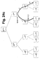
- FIG. 24 shows the structure of the address scheme of a one-dimensional CT tree.
- the rectangles symbolize a CT.
- the address of the CT is entered. indicates irrelevant address bits that are not evaluated, the relevant address bits are indicated with binary 0 or 1, * stands for any address bit.
- FIG. 24a shows the addressing from CT 0001.
- FIG. 24a shows the structure of the address scheme of a one-dimensional CT tree.
- the rectangles symbolize a CT.
- the address of the CT is entered. indicates irrelevant address bits that are not evaluated, the relevant address bits are indicated with binary 0 or 1, * stands for any address bit.
- FIG. 24a shows the addressing from CT 0001.
- the CT 0010 calls the relative address +10.
- FIG. 24c shows the known method over two levels in the positive direction and FIG. 24d shows the method over three levels in the negative direction with negative overflow.
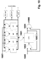
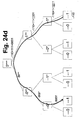
- FIG. 25 shows the structure of a 2-dimensional CT tree.
- the CTs (2501) are arranged in two dimensions on the lowest level (2502).
- the address of the dimension is indicated with x / y in the respective CT.
- 2502 is the next higher level (2504).
- Their CTs (2503) each control a group of 4 CTs of level 2502.
- the address space of the CTs on 2504 is one bit further, * indicates the address bits of level 2502, which are irrelevant for the selection of the CTs on 2504.
- the ROOT-CT 2505 is superordinate to 2504. Its address is again one bit further, the meaning of * is equivalent.
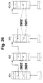
- Figure 26 shows the concatenation of the garbage collector in the microcontroller implementation. All KRs are linked together via the header entries (garbage-previous / garbage-next).
- the garbage collector runs through the list, the age of the KR is logged by increasing the entry by (+1) for the cache statistics (2602).
- the garbage collector looks for the KR statistics entry (2601), which indicates whether the KR is still in the FILMO list. In this case, the KR must not be deleted from GC, since it still contains unconfigured KW. Alternatively, this test could also be carried out using the FILMO-next and FILMO-previous entries.
- FIG. 27 shows the concatenation of the FILMO list.
- the chaining can be completely different than in the garbage list (FIG. 26).
- the KRs are linked via FILMO-previous and FILMO-next.
- the entries KR statistics (2701) point to the first KW not yet configured in the respective KR.
- a FILMO run is structured in such a way that the KR is started in the first ID. After execution, the position of the KW not executed is written after 2701. If KR has been executed completely, the KR is removed from the linked FILMO list, but remains in memory. Then the FILMO list jumps to the next KR, which is also processed.
- Figure 28 illustrates the structure of a KR in microcontroller control.
- the FILMO bit (2802) is assigned to each KW.
- a 1 (2803) indicates that the KW has been accepted by the CEL (ACCEPT) and will no longer be executed on the next run.
- a 0 (2804) indicates a REJECT, the KW must be executed again the next time.
- the optional KR statistic (2701) points to the first KW marked with 0. If PUSHRET (2805) receives a REJECT, the processing of the KR is interrupted here and the next run either on the first KW or at the point on which 2701 points again. Otherwise the KR is left properly at its end at 2806.
- FIG. 29 shows the circuit for saving the status information of a CEL before going through the FILMO or starting a KR.
- the status information is transferred from the CEL (2901) to a register (2902).
- the CT Before going through the FILMO or starting a KR, the CT sends an enable signal (2903) to 2902.
- the status information is then accepted and forwarded to the CT (2904). 2904 remains constant until the next submission of 2903.
- ACCEPT signal which indicates that the addressed CEL is in a configurable state and accepts the transmitted KW.
- Block commands including BLOCK-MOVE
- the source address of the data to be moved, the destination address of the data and the length of the data block are specified.
- Broadcast Send information to a variety of recipients.
- Data sender The unit (s) that provide data for the CEL as operands
- Data word A data word consists of an arbitrarily long row of bits. This row of bits represents a processing unit for a system. In a data word, commands for processors or the like can be used. Blocks as well as data are encoded.
- FILMO Modified FIFO from which data is read linearly. There is no restriction of the read pointer to the beginning of the memory.
- FPGA programmable logic device State of the art. F-PLUREG register in which the function of the CEL is set. The OneShot and Sleep modes are also set. The register is written by the PLU.
- Garbage collector unit for managing the memory. Prevents fragmentation.
- IDLE cycle Cycle in which a state machine does no processing.
- INITER-CT-BUS bus system between the CTs of a level and a higher CT (or CT group).
- INITIATOR CT which starts access to the Inter-CT bus.
- Pointer pointer to an address or a data word.
- a configurable element represents a unit of a logic module, which can be set by a configuration word for a special function. Configurable elements are therefore all types of RAM cells, multiplexers, arithmetic logic units, registers and all types of internal and external networking description etc. ⁇
- Configuration data Any number of configuration words.
- Configuration memory contains one or more configuration words.
- Configuration word A configuration word consists of any length of bits. This bit row represents a valid setting for the element to be configured, so that a functional unit is created.
- Loading logic unit for configuring and reconfiguring the CEL. Designed by a microcontroller specially adapted to its task.
- Logic cells Configurable cells used in DFPs, FPGAs, DPGAs that perform simple logic or arithmetic tasks according to their configuration.
- LUT1 lookup table that translates a trigger to an ID and determines whether the trigger is associated with a valid ID.
- LUT2 lookup table which translates an ID to the address of the corresponding KR in the local memory and determines whether the KR is present in the local memory.
- Mask bit combination that specifies the valid signals within a plurality of signals.
- RECONFIG trigger Set a CEL to the reconfigurable state.
- REJECT signal which indicates that the addressed CEL is in a non-configurable state and does not accept the transmitted KW.
- REMOVE- ⁇ ID> 1. Command within a KR to remove the KR referenced by ID. 2. Command of a higher-level CT via a separate interface or handshaking to a lower-level CT to delete the KR referenced by ID.
- ROOT-CT CT of the highest hierarchical level with direct access to the external configuration memory.
- Round-robin arbiter Arbiter that runs in a circle and always assigns the lowest priority to the signal that was arbitrated last.
- Synchronization signals Status signals that are generated by a configurable element or an arithmetic unit and are forwarded to other configurable elements or arithmetic units for control and synchronization of the data processing. It is also possible to return a synchronization signal with a time delay (stored) to one and the same configurable element or arithmetic unit.
- TARGET CT which is a target of access to the inter-CT bus.
- Trigger synonymous with synchronization signals.
- Reconfiguration New configuration of any set of CELs while any remaining set of CELs continue their own functions (see configure).
- State machine logic that can assume various states. The transitions between the states depend on different input parameters. These machines are used to control complex functions and correspond to the state of the art.
Claims (12)
- Procédé pour la mise en antémémoire d'instructions dans des microprocesseurs composés de plusieurs unités arithmétiques et dans des modules ayant une structure de cellules bi-ou multidimensionnelle (FPGA, DGPA, DFP ou analogues), caractérisé par le fait que1.1 plusieurs cellules et unités arithmétiques (CEL) sont réunies en un grand nombre de groupes, une unité d'antémémoire (CT) étant affectée à chaque sous-groupe,1.2 les unités d'antémémoire des différents sous-groupes sont connectées par une structure en arbre à une unité d'antémémoire supérieure (ROOT-CT) qui peut accéder à la mémoire d'instructions (ECR) dans laquelle sont stockées les instructions,1.3 les instructions sont regroupées en séquences d'instructions (KR) qui sont toujours mises en antémémoire et transmises entre les antémémoires en bloc,1.4 chaque unité d'antémémoire située au niveau inférieur ou intermédiaire de l'arbre demande les instructions nécessaires à l'unité d'antémémoire respectivement supérieure,1.5 une unité d'antémémoire supérieure envoie les séquences d'instructions demandées à l'unité inférieure si elle détient les séquences d'instructions dans sa mémoire locale,1.6 une unité d'antémémoire supérieure demande les séquences d'instructions à l'unité d'antémémoire qui lui est supérieure si elle ne détient pas les séquences d'instructions dans sa mémoire locale.
- Procédé selon la revendication 1, caractérisé par le fait que
les séquences d'instructions sont effacées en bloc. - Procédé selon les revendications 1 à 2, caractérisé par le fait que
des séquences d'instructions d'une unité d'antémémoire sont effacées lorsqu'il n'y a pas assez de place disponible pour charger une autre séquence d'instructions demandée dans la mémoire locale. - Procédé selon les revendications 1 à 2, caractérisé par le fait que
une instruction (REMOVE) au sein d'une séquence d'instructions déclenche un processus entraínant l'effacement de séquences d'instructions d'une unité d'antémémoire. - Procédé selon les revendications 1 à 4, caractérisé par le fait que
une instruction (EXECUTE) au sein d'une séquence d'instructions déclenche le chargement d'une séquence d'instructions donnée complète. - Procédé selon les revendications 1 à 5, caractérisé par le fait que
une instruction quelconque (EXECUTE, REMOVE, etc.) déclenche une action correspondante à l'instruction sur une unité d'antémémoire d'adresse quelconque via une liaison par bus entre les unités d'antémémoire. - Procédé selon les revendications 1 à 6, caractérisé par le fait que
une séquence de programme qui n'est pas effectivement cachable, car n'étant utilisée que par une unité d'antémémoire, est décomposée en petites sous-séquences nécessaires à plusieurs unités d'antémémoire, une autre sous-séquence (IKR) contenant le reste non cachable de la séquence d'instructions et les appels des sous-séquences cachables. - Procédé selon les revendications 1 à 7, caractérisé par le fait que
à chaque séquence d'instructions est associée une statistique qui donne des informations sur l'âge, c'est-à-dire la durée de séjour dans la mémoire de l'unité d'antémémoire, de la séquence d'instructions. - Procédé selon les revendications 1 à 7, caractérisé par le fait que
à chaque séquence d'instructions est associée une statistique qui donne des informations sur la fréquence des appels de la séquence d'instructions. - Procédé selon les revendications 1 à 7, caractérisé par le fait que
à chaque séquence d'instructions est associée une statistique qui donne des informations sur la longueur de la séquence d'instructions. - Procédé selon les revendications 1 à 10, caractérisé par le fait que
la routine d'effacement est conçue de manière à évaluer la statistique de chaque séquence d'instructions et à supprimer la séquence d'instructions la moins importante en fonction de l'algorithme exécuté. - Procédé selon les revendications 1 à 11, caractérisé par le fait que
la routine d'effacement est adaptable par programmation à l'algorithme à exécuter.
Priority Applications (2)
| Application Number | Priority Date | Filing Date | Title |
|---|---|---|---|
| EP01120095A EP1164474A3 (fr) | 1998-02-25 | 1999-02-25 | Méthode pour cacher hiérarchiquement des données de configuration de processeurs de flux de données |
| EP10012017A EP2293193A1 (fr) | 1998-02-25 | 1999-02-25 | Procédé et dispositif de traitement de données |
Applications Claiming Priority (3)
| Application Number | Priority Date | Filing Date | Title |
|---|---|---|---|
| DE19807872A DE19807872A1 (de) | 1998-02-25 | 1998-02-25 | Verfahren zur Verwaltung von Konfigurationsdaten in Datenflußprozessoren sowie Bausteinen mit zwei- oder mehrdimensionalen programmierbaren Zellstruktur (FPGAs, DPGAs, o. dgl. |
| DE19807872 | 1998-02-25 | ||
| PCT/DE1999/000504 WO1999044147A2 (fr) | 1998-02-25 | 1999-02-25 | PROCEDE POUR LA MISE EN ANTEMEMOIRE HIERARCHIQUE DE DONNEES DE CONFIGURATION DE PROCESSEURS DE FLUX DE DONNEES ET DE MODULES AVEC UNE STRUCTURE DE CELLULE PROGRAMMABLE BI- OU MUTLIDIMENSIONNELLE (FPGAs, DPGAs OU ANALOGUE) |
Related Child Applications (2)
| Application Number | Title | Priority Date | Filing Date |
|---|---|---|---|
| EP01120095A Division EP1164474A3 (fr) | 1998-02-25 | 1999-02-25 | Méthode pour cacher hiérarchiquement des données de configuration de processeurs de flux de données |
| EP01120095.3 Division-Into | 2001-08-21 |
Publications (2)
| Publication Number | Publication Date |
|---|---|
| EP1057117A2 EP1057117A2 (fr) | 2000-12-06 |
| EP1057117B1 true EP1057117B1 (fr) | 2002-05-15 |
Family
ID=7858839
Family Applications (4)
| Application Number | Title | Priority Date | Filing Date |
|---|---|---|---|
| EP10012017A Withdrawn EP2293193A1 (fr) | 1998-02-25 | 1999-02-25 | Procédé et dispositif de traitement de données |
| EP01120095A Withdrawn EP1164474A3 (fr) | 1998-02-25 | 1999-02-25 | Méthode pour cacher hiérarchiquement des données de configuration de processeurs de flux de données |
| EP99913087A Expired - Lifetime EP1057117B1 (fr) | 1998-02-25 | 1999-02-25 | PROCEDE POUR LA MISE EN ANTEMEMOIRE HIERARCHIQUE DE DONNEES DE CONFIGURATION DE PROCESSEURS DE FLUX DE DONNEES ET DE MODULES AVEC UNE STRUCTURE DE CELLULE PROGRAMMABLE BI- OU MUTLIDIMENSIONNELLE (FPGAs, DPGAs OU ANALOGUE) |
| EP99914430A Expired - Lifetime EP1057102B1 (fr) | 1998-02-25 | 1999-02-25 | PROCEDE POUR LA CONFIGURATION SANS INTERBLOCAGE DE PROCESSEURS DE FLUX DE DONNEES ET DE MODULES AVEC UNE STRUCTURE DE CELLULE PROGRAMMABLE BI- OU MULTIDIMENSIONNELLE (FPGAs, DPGAs OU ANALOGUE) |
Family Applications Before (2)
| Application Number | Title | Priority Date | Filing Date |
|---|---|---|---|
| EP10012017A Withdrawn EP2293193A1 (fr) | 1998-02-25 | 1999-02-25 | Procédé et dispositif de traitement de données |
| EP01120095A Withdrawn EP1164474A3 (fr) | 1998-02-25 | 1999-02-25 | Méthode pour cacher hiérarchiquement des données de configuration de processeurs de flux de données |
Family Applications After (1)
| Application Number | Title | Priority Date | Filing Date |
|---|---|---|---|
| EP99914430A Expired - Lifetime EP1057102B1 (fr) | 1998-02-25 | 1999-02-25 | PROCEDE POUR LA CONFIGURATION SANS INTERBLOCAGE DE PROCESSEURS DE FLUX DE DONNEES ET DE MODULES AVEC UNE STRUCTURE DE CELLULE PROGRAMMABLE BI- OU MULTIDIMENSIONNELLE (FPGAs, DPGAs OU ANALOGUE) |
Country Status (10)
| Country | Link |
|---|---|
| US (3) | US6571381B1 (fr) |
| EP (4) | EP2293193A1 (fr) |
| JP (2) | JP4338308B2 (fr) |
| CN (2) | CN1298521A (fr) |
| AT (2) | ATE217713T1 (fr) |
| AU (2) | AU3326299A (fr) |
| CA (2) | CA2321874A1 (fr) |
| DE (5) | DE19807872A1 (fr) |
| EA (2) | EA003407B1 (fr) |
| WO (2) | WO1999044120A2 (fr) |
Families Citing this family (106)
| Publication number | Priority date | Publication date | Assignee | Title |
|---|---|---|---|---|
| WO2003025781A2 (fr) * | 2001-09-19 | 2003-03-27 | Pact Xpp Technologies Ag | Routeur |
| US7266725B2 (en) | 2001-09-03 | 2007-09-04 | Pact Xpp Technologies Ag | Method for debugging reconfigurable architectures |
| US6205249B1 (en) | 1998-04-02 | 2001-03-20 | Scott A. Moskowitz | Multiple transform utilization and applications for secure digital watermarking |
| US7664263B2 (en) | 1998-03-24 | 2010-02-16 | Moskowitz Scott A | Method for combining transfer functions with predetermined key creation |
| US7346472B1 (en) | 2000-09-07 | 2008-03-18 | Blue Spike, Inc. | Method and device for monitoring and analyzing signals |
| US7457962B2 (en) | 1996-07-02 | 2008-11-25 | Wistaria Trading, Inc | Optimization methods for the insertion, protection, and detection of digital watermarks in digitized data |
| US7177429B2 (en) | 2000-12-07 | 2007-02-13 | Blue Spike, Inc. | System and methods for permitting open access to data objects and for securing data within the data objects |
| US7095874B2 (en) | 1996-07-02 | 2006-08-22 | Wistaria Trading, Inc. | Optimization methods for the insertion, protection, and detection of digital watermarks in digitized data |
| US7159116B2 (en) | 1999-12-07 | 2007-01-02 | Blue Spike, Inc. | Systems, methods and devices for trusted transactions |
| DE19651075A1 (de) * | 1996-12-09 | 1998-06-10 | Pact Inf Tech Gmbh | Einheit zur Verarbeitung von numerischen und logischen Operationen, zum Einsatz in Prozessoren (CPU's), Mehrrechnersystemen, Datenflußprozessoren (DFP's), digitalen Signal Prozessoren (DSP's) oder dergleichen |
| DE19654595A1 (de) | 1996-12-20 | 1998-07-02 | Pact Inf Tech Gmbh | I0- und Speicherbussystem für DFPs sowie Bausteinen mit zwei- oder mehrdimensionaler programmierbaren Zellstrukturen |
| EP1329816B1 (fr) | 1996-12-27 | 2011-06-22 | Richter, Thomas | Procédé pour le transfert dynamique automatique de processeurs à flux de données (dfp) ainsi que de modules à deux ou plusieurs structures cellulaires programmables bidimensionnelles ou multidimensionnelles (fpga, dpga ou analogues) |
| DE19654846A1 (de) * | 1996-12-27 | 1998-07-09 | Pact Inf Tech Gmbh | Verfahren zum selbständigen dynamischen Umladen von Datenflußprozessoren (DFPs) sowie Bausteinen mit zwei- oder mehrdimensionalen programmierbaren Zellstrukturen (FPGAs, DPGAs, o. dgl.) |
| US6542998B1 (en) | 1997-02-08 | 2003-04-01 | Pact Gmbh | Method of self-synchronization of configurable elements of a programmable module |
| DE19704728A1 (de) * | 1997-02-08 | 1998-08-13 | Pact Inf Tech Gmbh | Verfahren zur Selbstsynchronisation von konfigurierbaren Elementen eines programmierbaren Bausteines |
| DE19704742A1 (de) * | 1997-02-11 | 1998-09-24 | Pact Inf Tech Gmbh | Internes Bussystem für DFPs, sowie Bausteinen mit zwei- oder mehrdimensionalen programmierbaren Zellstrukturen, zur Bewältigung großer Datenmengen mit hohem Vernetzungsaufwand |
| US8686549B2 (en) | 2001-09-03 | 2014-04-01 | Martin Vorbach | Reconfigurable elements |
| DE19861088A1 (de) | 1997-12-22 | 2000-02-10 | Pact Inf Tech Gmbh | Verfahren zur Reparatur von integrierten Schaltkreisen |
| US7664264B2 (en) | 1999-03-24 | 2010-02-16 | Blue Spike, Inc. | Utilizing data reduction in steganographic and cryptographic systems |
| EP1228440B1 (fr) | 1999-06-10 | 2017-04-05 | PACT XPP Technologies AG | Partionnement de séquences dans des structures cellulaires |
| WO2001018628A2 (fr) * | 1999-08-04 | 2001-03-15 | Blue Spike, Inc. | Serveur de contenu personnel securise |
| DE19946752A1 (de) * | 1999-09-29 | 2001-04-12 | Infineon Technologies Ag | Rekonfigurierbares Gate-Array |
| ATE476700T1 (de) | 2000-06-13 | 2010-08-15 | Richter Thomas | Pipeline ct-protokolle und -kommunikation |
| US7127615B2 (en) | 2000-09-20 | 2006-10-24 | Blue Spike, Inc. | Security based on subliminal and supraliminal channels for data objects |
| US7502920B2 (en) * | 2000-10-03 | 2009-03-10 | Intel Corporation | Hierarchical storage architecture for reconfigurable logic configurations |
| US20040015899A1 (en) * | 2000-10-06 | 2004-01-22 | Frank May | Method for processing data |
| US8058899B2 (en) | 2000-10-06 | 2011-11-15 | Martin Vorbach | Logic cell array and bus system |
| GB2406416A (en) * | 2000-10-31 | 2005-03-30 | Advanced Risc Mach Ltd | Describing an integrated circuit configuration |
| US7844796B2 (en) | 2001-03-05 | 2010-11-30 | Martin Vorbach | Data processing device and method |
| US20090210653A1 (en) * | 2001-03-05 | 2009-08-20 | Pact Xpp Technologies Ag | Method and device for treating and processing data |
| WO2005045692A2 (fr) | 2003-08-28 | 2005-05-19 | Pact Xpp Technologies Ag | Dispositif et procede de traitement de donnees |
| US7210129B2 (en) * | 2001-08-16 | 2007-04-24 | Pact Xpp Technologies Ag | Method for translating programs for reconfigurable architectures |
| AU2002254921A1 (en) | 2001-03-05 | 2002-09-19 | Pact Informationstechnologie Gmbh | Methods and devices for treating and processing data |
| US20090300262A1 (en) * | 2001-03-05 | 2009-12-03 | Martin Vorbach | Methods and devices for treating and/or processing data |
| US7444531B2 (en) | 2001-03-05 | 2008-10-28 | Pact Xpp Technologies Ag | Methods and devices for treating and processing data |
| US9037807B2 (en) * | 2001-03-05 | 2015-05-19 | Pact Xpp Technologies Ag | Processor arrangement on a chip including data processing, memory, and interface elements |
| US7624204B2 (en) * | 2001-03-22 | 2009-11-24 | Nvidia Corporation | Input/output controller node in an adaptable computing environment |
| JP2004533691A (ja) | 2001-06-20 | 2004-11-04 | ペーアーツェーテー イクスペーペー テクノロジーズ アクチエンゲゼルシャフト | データを処理するための方法 |
| US7996827B2 (en) | 2001-08-16 | 2011-08-09 | Martin Vorbach | Method for the translation of programs for reconfigurable architectures |
| US7434191B2 (en) * | 2001-09-03 | 2008-10-07 | Pact Xpp Technologies Ag | Router |
| JP4152319B2 (ja) * | 2001-09-07 | 2008-09-17 | アイピーフレックス株式会社 | データ処理システムおよびその制御方法 |
| US8686475B2 (en) | 2001-09-19 | 2014-04-01 | Pact Xpp Technologies Ag | Reconfigurable elements |
| DE10147772C1 (de) * | 2001-09-27 | 2003-09-11 | Siemens Ag | Verfahren zum Betreiben eines Übertragungssystems und Übertragungssystem in einem Energieversorgungsnetz |
| US7594229B2 (en) * | 2001-10-09 | 2009-09-22 | Nvidia Corp. | Predictive resource allocation in computing systems |
| US7644279B2 (en) * | 2001-12-05 | 2010-01-05 | Nvidia Corporation | Consumer product distribution in the embedded system market |
| US7577822B2 (en) * | 2001-12-14 | 2009-08-18 | Pact Xpp Technologies Ag | Parallel task operation in processor and reconfigurable coprocessor configured based on information in link list including termination information for synchronization |
| US20050132344A1 (en) * | 2002-01-18 | 2005-06-16 | Martin Vorbach | Method of compilation |
| WO2003060747A2 (fr) | 2002-01-19 | 2003-07-24 | Pact Xpp Technologies Ag | Processeur reconfigurable |
| AU2003214003A1 (en) | 2002-02-18 | 2003-09-09 | Pact Xpp Technologies Ag | Bus systems and method for reconfiguration |
| WO2003081454A2 (fr) * | 2002-03-21 | 2003-10-02 | Pact Xpp Technologies Ag | Procede et dispositif de traitement de donnees |
| US8914590B2 (en) | 2002-08-07 | 2014-12-16 | Pact Xpp Technologies Ag | Data processing method and device |
| JP4501914B2 (ja) * | 2002-04-03 | 2010-07-14 | ソニー株式会社 | 集積回路、および集積回路装置 |
| US7287275B2 (en) | 2002-04-17 | 2007-10-23 | Moskowitz Scott A | Methods, systems and devices for packet watermarking and efficient provisioning of bandwidth |
| US7093255B1 (en) * | 2002-05-31 | 2006-08-15 | Quicksilver Technology, Inc. | Method for estimating cost when placing operations within a modulo scheduler when scheduling for processors with a large number of function units or reconfigurable data paths |
| US7620678B1 (en) | 2002-06-12 | 2009-11-17 | Nvidia Corporation | Method and system for reducing the time-to-market concerns for embedded system design |
| US7802108B1 (en) | 2002-07-18 | 2010-09-21 | Nvidia Corporation | Secure storage of program code for an embedded system |
| US20110238948A1 (en) * | 2002-08-07 | 2011-09-29 | Martin Vorbach | Method and device for coupling a data processing unit and a data processing array |
| AU2003286131A1 (en) | 2002-08-07 | 2004-03-19 | Pact Xpp Technologies Ag | Method and device for processing data |
| US7657861B2 (en) | 2002-08-07 | 2010-02-02 | Pact Xpp Technologies Ag | Method and device for processing data |
| US7249352B2 (en) * | 2002-08-22 | 2007-07-24 | International Business Machines Corporation | Apparatus and method for removing elements from a linked list |
| JP4388895B2 (ja) | 2002-09-06 | 2009-12-24 | ペーアーツェーテー イクスペーペー テクノロジーズ アクチエンゲゼルシャフト | リコンフィギュアラブルなシーケンサ構造 |
| US7502915B2 (en) * | 2002-09-30 | 2009-03-10 | Nvidia Corporation | System and method using embedded microprocessor as a node in an adaptable computing machine |
| US8949576B2 (en) * | 2002-11-01 | 2015-02-03 | Nvidia Corporation | Arithmetic node including general digital signal processing functions for an adaptive computing machine |
| US7617100B1 (en) | 2003-01-10 | 2009-11-10 | Nvidia Corporation | Method and system for providing an excitation-pattern based audio coding scheme |
| JP2006524850A (ja) * | 2003-04-04 | 2006-11-02 | ペーアーツェーテー イクスペーペー テクノロジーズ アクチエンゲゼルシャフト | データ処理方法およびデータ処理装置 |
| US9330060B1 (en) * | 2003-04-15 | 2016-05-03 | Nvidia Corporation | Method and device for encoding and decoding video image data |
| US7565677B1 (en) | 2003-04-21 | 2009-07-21 | Microsoft Corporation | Method and apparatus for managing a data carousel |
| US7450600B2 (en) * | 2003-04-21 | 2008-11-11 | Microsoft Corporation | Method and apparatus for managing a data carousel |
| US8660182B2 (en) * | 2003-06-09 | 2014-02-25 | Nvidia Corporation | MPEG motion estimation based on dual start points |
| US7603542B2 (en) * | 2003-06-25 | 2009-10-13 | Nec Corporation | Reconfigurable electric computer, semiconductor integrated circuit and control method, program generation method, and program for creating a logic circuit from an application program |
| US8296764B2 (en) * | 2003-08-14 | 2012-10-23 | Nvidia Corporation | Internal synchronization control for adaptive integrated circuitry |
| US7484045B2 (en) * | 2004-03-30 | 2009-01-27 | Intel Corporation | Store performance in strongly-ordered microprocessor architecture |
| US8130825B2 (en) * | 2004-05-10 | 2012-03-06 | Nvidia Corporation | Processor for video data encoding/decoding |
| US8018463B2 (en) | 2004-05-10 | 2011-09-13 | Nvidia Corporation | Processor for video data |
| US7278122B2 (en) * | 2004-06-24 | 2007-10-02 | Ftl Systems, Inc. | Hardware/software design tool and language specification mechanism enabling efficient technology retargeting and optimization |
| TWI256013B (en) * | 2004-10-12 | 2006-06-01 | Uli Electronics Inc | Sound-effect processing circuit |
| EP1849095B1 (fr) * | 2005-02-07 | 2013-01-02 | Richter, Thomas | Dispositif de traitement de donnees massivement parallele a faible latence |
| CN100476795C (zh) * | 2005-02-21 | 2009-04-08 | 徐建 | 事件处理机 |
| CN101194472B (zh) * | 2005-06-01 | 2012-07-18 | 西门子公司 | 具有独立软件模块的测量或保护设备以及保护系统 |
| WO2007062327A2 (fr) * | 2005-11-18 | 2007-05-31 | Ideal Industries, Inc. | Connecteur de fils liberable |
| US8731071B1 (en) | 2005-12-15 | 2014-05-20 | Nvidia Corporation | System for performing finite input response (FIR) filtering in motion estimation |
| EP1974265A1 (fr) | 2006-01-18 | 2008-10-01 | PACT XPP Technologies AG | Procédé de définition de matériels |
| US8724702B1 (en) | 2006-03-29 | 2014-05-13 | Nvidia Corporation | Methods and systems for motion estimation used in video coding |
| US7827451B2 (en) * | 2006-05-24 | 2010-11-02 | International Business Machines Corporation | Method, system and program product for establishing decimal floating point operands for facilitating testing of decimal floating point instructions |
| US8660380B2 (en) * | 2006-08-25 | 2014-02-25 | Nvidia Corporation | Method and system for performing two-dimensional transform on data value array with reduced power consumption |
| JP5045036B2 (ja) * | 2006-09-05 | 2012-10-10 | 富士ゼロックス株式会社 | データ処理装置 |
| US7999820B1 (en) | 2006-10-23 | 2011-08-16 | Nvidia Corporation | Methods and systems for reusing memory addresses in a graphics system |
| US20080111923A1 (en) * | 2006-11-09 | 2008-05-15 | Scheuermann W James | Processor for video data |
| WO2008061161A2 (fr) * | 2006-11-14 | 2008-05-22 | Star Bridge Systems, Inc. | Exécution de code patrimonial sur une plate-forme hybride |
| US8169789B1 (en) | 2007-04-10 | 2012-05-01 | Nvidia Corporation | Graphics processing unit stiffening frame |
| US7987065B1 (en) | 2007-04-17 | 2011-07-26 | Nvidia Corporation | Automatic quality testing of multimedia rendering by software drivers |
| US8572598B1 (en) | 2007-04-18 | 2013-10-29 | Nvidia Corporation | Method and system for upgrading software in a computing device |
| US20080291209A1 (en) * | 2007-05-25 | 2008-11-27 | Nvidia Corporation | Encoding Multi-media Signals |
| US8756482B2 (en) * | 2007-05-25 | 2014-06-17 | Nvidia Corporation | Efficient encoding/decoding of a sequence of data frames |
| US8726283B1 (en) | 2007-06-04 | 2014-05-13 | Nvidia Corporation | Deadlock avoidance skid buffer |
| US7948500B2 (en) * | 2007-06-07 | 2011-05-24 | Nvidia Corporation | Extrapolation of nonresident mipmap data using resident mipmap data |
| US7944453B1 (en) | 2007-06-07 | 2011-05-17 | Nvidia Corporation | Extrapolation texture filtering for nonresident mipmaps |
| US9118927B2 (en) * | 2007-06-13 | 2015-08-25 | Nvidia Corporation | Sub-pixel interpolation and its application in motion compensated encoding of a video signal |
| US8873625B2 (en) | 2007-07-18 | 2014-10-28 | Nvidia Corporation | Enhanced compression in representing non-frame-edge blocks of image frames |
| JP5294304B2 (ja) * | 2008-06-18 | 2013-09-18 | 日本電気株式会社 | 再構成可能電子回路装置 |
| US8598990B2 (en) * | 2008-06-30 | 2013-12-03 | Symbol Technologies, Inc. | Delimited read command for efficient data access from radio frequency identification (RFID) tags |
| US8666181B2 (en) * | 2008-12-10 | 2014-03-04 | Nvidia Corporation | Adaptive multiple engine image motion detection system and method |
| WO2010142432A2 (fr) | 2009-06-09 | 2010-12-16 | Martin Vorbach | Système et procédé d'antémémoire dans un processeur multi-cœur |
| JP2016178229A (ja) | 2015-03-20 | 2016-10-06 | 株式会社東芝 | 再構成可能な回路 |
| JP6672190B2 (ja) * | 2017-01-16 | 2020-03-25 | 株式会社東芝 | データベースシステムおよびデータ処理方法 |
| US11803507B2 (en) | 2018-10-29 | 2023-10-31 | Secturion Systems, Inc. | Data stream protocol field decoding by a systolic array |
Family Cites Families (152)
| Publication number | Priority date | Publication date | Assignee | Title |
|---|---|---|---|---|
| JPS5936857A (ja) | 1982-08-25 | 1984-02-29 | Nec Corp | プロセツサユニツト |
| US4739474A (en) | 1983-03-10 | 1988-04-19 | Martin Marietta Corporation | Geometric-arithmetic parallel processor |
| US5123109A (en) | 1983-05-31 | 1992-06-16 | Thinking Machines Corporation | Parallel processor including a processor array with plural data transfer arrangements including (1) a global router and (2) a proximate-neighbor transfer system |
| USRE34363E (en) | 1984-03-12 | 1993-08-31 | Xilinx, Inc. | Configurable electrical circuit having configurable logic elements and configurable interconnects |
| US4870302A (en) | 1984-03-12 | 1989-09-26 | Xilinx, Inc. | Configurable electrical circuit having configurable logic elements and configurable interconnects |
| US4761755A (en) | 1984-07-11 | 1988-08-02 | Prime Computer, Inc. | Data processing system and method having an improved arithmetic unit |
| US5023775A (en) | 1985-02-14 | 1991-06-11 | Intel Corporation | Software programmable logic array utilizing "and" and "or" gates |
| US5247689A (en) | 1985-02-25 | 1993-09-21 | Ewert Alfred P | Parallel digital processor including lateral transfer buses with interrupt switches to form bus interconnection segments |
| US4706216A (en) | 1985-02-27 | 1987-11-10 | Xilinx, Inc. | Configurable logic element |
| US5225719A (en) | 1985-03-29 | 1993-07-06 | Advanced Micro Devices, Inc. | Family of multiple segmented programmable logic blocks interconnected by a high speed centralized switch matrix |
| US5015884A (en) | 1985-03-29 | 1991-05-14 | Advanced Micro Devices, Inc. | Multiple array high performance programmable logic device family |
| US4967340A (en) | 1985-06-12 | 1990-10-30 | E-Systems, Inc. | Adaptive processing system having an array of individually configurable processing components |
| EP0221360B1 (fr) | 1985-11-04 | 1992-12-30 | International Business Machines Corporation | Réseaux de transmission de messages numériques et établissement des voies de communication dans ces réseaux |
| US4852048A (en) | 1985-12-12 | 1989-07-25 | Itt Corporation | Single instruction multiple data (SIMD) cellular array processing apparatus employing a common bus where a first number of bits manifest a first bus portion and a second number of bits manifest a second bus portion |
| US5021947A (en) | 1986-03-31 | 1991-06-04 | Hughes Aircraft Company | Data-flow multiprocessor architecture with three dimensional multistage interconnection network for efficient signal and data processing |
| US4860201A (en) * | 1986-09-02 | 1989-08-22 | The Trustees Of Columbia University In The City Of New York | Binary tree parallel processor |
| US5367208A (en) | 1986-09-19 | 1994-11-22 | Actel Corporation | Reconfigurable programmable interconnect architecture |
| US4811214A (en) | 1986-11-14 | 1989-03-07 | Princeton University | Multinode reconfigurable pipeline computer |
| US5226122A (en) | 1987-08-21 | 1993-07-06 | Compaq Computer Corp. | Programmable logic system for filtering commands to a microprocessor |
| US5115510A (en) | 1987-10-20 | 1992-05-19 | Sharp Kabushiki Kaisha | Multistage data flow processor with instruction packet, fetch, storage transmission and address generation controlled by destination information |
| US4918690A (en) | 1987-11-10 | 1990-04-17 | Echelon Systems Corp. | Network and intelligent cell for providing sensing, bidirectional communications and control |
| US5113498A (en) | 1987-11-10 | 1992-05-12 | Echelon Corporation | Input/output section for an intelligent cell which provides sensing, bidirectional communications and control |
| US5303172A (en) | 1988-02-16 | 1994-04-12 | Array Microsystems | Pipelined combination and vector signal processor |
| US5204935A (en) | 1988-08-19 | 1993-04-20 | Fuji Xerox Co., Ltd. | Programmable fuzzy logic circuits |
| US4901268A (en) | 1988-08-19 | 1990-02-13 | General Electric Company | Multiple function data processor |
| US5353432A (en) * | 1988-09-09 | 1994-10-04 | Compaq Computer Corporation | Interactive method for configuration of computer system and circuit boards with user specification of system resources and computer resolution of resource conflicts |
| EP0363631B1 (fr) | 1988-09-22 | 1993-12-15 | Siemens Aktiengesellschaft | Circuit pour centraux de télécommunications, en particulier des centraux téléphoniques à division dans le temps MIC avec des réseaux de commutation distribués connectés à un réseau de commutation central |
| DE68926783T2 (de) | 1988-10-07 | 1996-11-28 | Martin Marietta Corp | Paralleler datenprozessor |
| US5014193A (en) | 1988-10-14 | 1991-05-07 | Compaq Computer Corporation | Dynamically configurable portable computer system |
| US5136717A (en) | 1988-11-23 | 1992-08-04 | Flavors Technology Inc. | Realtime systolic, multiple-instruction, single-data parallel computer system |
| US5081375A (en) | 1989-01-19 | 1992-01-14 | National Semiconductor Corp. | Method for operating a multiple page programmable logic device |
| GB8906145D0 (en) | 1989-03-17 | 1989-05-04 | Algotronix Ltd | Configurable cellular array |
| US5203005A (en) | 1989-05-02 | 1993-04-13 | Horst Robert W | Cell structure for linear array wafer scale integration architecture with capability to open boundary i/o bus without neighbor acknowledgement |
| US5109503A (en) | 1989-05-22 | 1992-04-28 | Ge Fanuc Automation North America, Inc. | Apparatus with reconfigurable counter includes memory for storing plurality of counter configuration files which respectively define plurality of predetermined counters |
| US5212652A (en) | 1989-08-15 | 1993-05-18 | Advanced Micro Devices, Inc. | Programmable gate array with improved interconnect structure |
| US5489857A (en) | 1992-08-03 | 1996-02-06 | Advanced Micro Devices, Inc. | Flexible synchronous/asynchronous cell structure for a high density programmable logic device |
| US5233539A (en) | 1989-08-15 | 1993-08-03 | Advanced Micro Devices, Inc. | Programmable gate array with improved interconnect structure, input/output structure and configurable logic block |
| US5128559A (en) | 1989-09-29 | 1992-07-07 | Sgs-Thomson Microelectronics, Inc. | Logic block for programmable logic devices |
| JP2968289B2 (ja) | 1989-11-08 | 1999-10-25 | 株式会社リコー | 中央演算処理装置 |
| GB8925721D0 (en) | 1989-11-14 | 1990-01-04 | Amt Holdings | Processor array system |
| US5522083A (en) | 1989-11-17 | 1996-05-28 | Texas Instruments Incorporated | Reconfigurable multi-processor operating in SIMD mode with one processor fetching instructions for use by remaining processors |
| US5125801A (en) | 1990-02-02 | 1992-06-30 | Isco, Inc. | Pumping system |
| US5142469A (en) | 1990-03-29 | 1992-08-25 | Ge Fanuc Automation North America, Inc. | Method for converting a programmable logic controller hardware configuration and corresponding control program for use on a first programmable logic controller to use on a second programmable logic controller |
| US5198705A (en) | 1990-05-11 | 1993-03-30 | Actel Corporation | Logic module with configurable combinational and sequential blocks |
| US5483620A (en) | 1990-05-22 | 1996-01-09 | International Business Machines Corp. | Learning machine synapse processor system apparatus |
| US5111079A (en) | 1990-06-29 | 1992-05-05 | Sgs-Thomson Microelectronics, Inc. | Power reduction circuit for programmable logic device |
| SE9002558D0 (sv) | 1990-08-02 | 1990-08-02 | Carlstedt Elektronik Ab | Processor |
| US5708836A (en) | 1990-11-13 | 1998-01-13 | International Business Machines Corporation | SIMD/MIMD inter-processor communication |
| US5734921A (en) | 1990-11-13 | 1998-03-31 | International Business Machines Corporation | Advanced parallel array processor computer package |
| US5765011A (en) | 1990-11-13 | 1998-06-09 | International Business Machines Corporation | Parallel processing system having a synchronous SIMD processing with processing elements emulating SIMD operation using individual instruction streams |
| US5588152A (en) | 1990-11-13 | 1996-12-24 | International Business Machines Corporation | Advanced parallel processor including advanced support hardware |
| US5590345A (en) | 1990-11-13 | 1996-12-31 | International Business Machines Corporation | Advanced parallel array processor(APAP) |
| CA2051222C (fr) * | 1990-11-30 | 1998-05-05 | Pradeep S. Sindhu | Bus de memoire coherent a commutation de paquets pour multiprocesseurs a memoire commune |
| US5301344A (en) | 1991-01-29 | 1994-04-05 | Analogic Corporation | Multibus sequential processor to perform in parallel a plurality of reconfigurable logic operations on a plurality of data sets |
| DE59109046D1 (de) | 1991-02-22 | 1998-10-08 | Siemens Ag | Programmierverfahren für einen Logikbaustein |
| JPH04290155A (ja) | 1991-03-19 | 1992-10-14 | Fujitsu Ltd | 並列データ処理方式 |
| JPH04293151A (ja) | 1991-03-20 | 1992-10-16 | Fujitsu Ltd | 並列データ処理方式 |
| US5617547A (en) | 1991-03-29 | 1997-04-01 | International Business Machines Corporation | Switch network extension of bus architecture |
| JPH04328657A (ja) * | 1991-04-30 | 1992-11-17 | Toshiba Corp | キャッシュメモリ |
| US5389431A (en) | 1991-05-14 | 1995-02-14 | Idemitsu Kosan Co., Ltd. | Nonwoven fabric and process for producing same |
| US5551033A (en) * | 1991-05-17 | 1996-08-27 | Zenith Data Systems Corporation | Apparatus for maintaining one interrupt mask register in conformity with another in a manner invisible to an executing program |
| WO1992022029A1 (fr) | 1991-05-24 | 1992-12-10 | British Technology Group Usa, Inc. | Optimisation de compilateur pour ordinateurs |
| US5659797A (en) | 1991-06-24 | 1997-08-19 | U.S. Philips Corporation | Sparc RISC based computer system including a single chip processor with memory management and DMA units coupled to a DRAM interface |
| US5338984A (en) | 1991-08-29 | 1994-08-16 | National Semiconductor Corp. | Local and express diagonal busses in a configurable logic array |
| US5260610A (en) | 1991-09-03 | 1993-11-09 | Altera Corporation | Programmable logic element interconnections for programmable logic array integrated circuits |
| AU2939892A (en) | 1991-12-06 | 1993-06-28 | Richard S. Norman | Massively-parallel direct output processor array |
| US5208491A (en) | 1992-01-07 | 1993-05-04 | Washington Research Foundation | Field programmable gate array |
| JP2791243B2 (ja) | 1992-03-13 | 1998-08-27 | 株式会社東芝 | 階層間同期化システムおよびこれを用いた大規模集積回路 |
| US5452401A (en) | 1992-03-31 | 1995-09-19 | Seiko Epson Corporation | Selective power-down for high performance CPU/system |
| US5611049A (en) * | 1992-06-03 | 1997-03-11 | Pitts; William M. | System for accessing distributed data cache channel at each network node to pass requests and data |
| EP0643855A1 (fr) | 1992-06-04 | 1995-03-22 | Xilinx, Inc. | Methode de commande par temporisation pour l'implantation d'un circuit d'utilisateur sur un dispositif de circuit integre programmable |
| DE4221278C2 (de) | 1992-06-29 | 1996-02-29 | Martin Vorbach | Busgekoppeltes Mehrrechnersystem |
| US5475803A (en) | 1992-07-10 | 1995-12-12 | Lsi Logic Corporation | Method for 2-D affine transformation of images |
| US5590348A (en) | 1992-07-28 | 1996-12-31 | International Business Machines Corporation | Status predictor for combined shifter-rotate/merge unit |
| US5684980A (en) * | 1992-07-29 | 1997-11-04 | Virtual Computer Corporation | FPGA virtual computer for executing a sequence of program instructions by successively reconfiguring a group of FPGA in response to those instructions |
| US5497498A (en) | 1992-11-05 | 1996-03-05 | Giga Operations Corporation | Video processing module using a second programmable logic device which reconfigures a first programmable logic device for data transformation |
| US5392437A (en) | 1992-11-06 | 1995-02-21 | Intel Corporation | Method and apparatus for independently stopping and restarting functional units |
| US5361373A (en) | 1992-12-11 | 1994-11-01 | Gilson Kent L | Integrated circuit computing device comprising a dynamically configurable gate array having a microprocessor and reconfigurable instruction execution means and method therefor |
| GB9303084D0 (en) | 1993-02-16 | 1993-03-31 | Inmos Ltd | Programmable logic circuit |
| JPH06276086A (ja) | 1993-03-18 | 1994-09-30 | Fuji Xerox Co Ltd | フィールドプログラマブルゲートアレイ |
| US5548773A (en) | 1993-03-30 | 1996-08-20 | The United States Of America As Represented By The Administrator Of The National Aeronautics And Space Administration | Digital parallel processor array for optimum path planning |
| US5596742A (en) | 1993-04-02 | 1997-01-21 | Massachusetts Institute Of Technology | Virtual interconnections for reconfigurable logic systems |
| US5473266A (en) | 1993-04-19 | 1995-12-05 | Altera Corporation | Programmable logic device having fast programmable logic array blocks and a central global interconnect array |
| DE4416881C2 (de) | 1993-05-13 | 1998-03-19 | Pact Inf Tech Gmbh | Verfahren zum Betrieb einer Datenverarbeitungseinrichtung |
| IL109921A (en) * | 1993-06-24 | 1997-09-30 | Quickturn Design Systems | Method and apparatus for configuring memory circuits |
| US5444394A (en) | 1993-07-08 | 1995-08-22 | Altera Corporation | PLD with selective inputs from local and global conductors |
| JPH0736858A (ja) | 1993-07-21 | 1995-02-07 | Hitachi Ltd | 信号処理プロセッサ |
| US5457644A (en) | 1993-08-20 | 1995-10-10 | Actel Corporation | Field programmable digital signal processing array integrated circuit |
| US5440538A (en) | 1993-09-23 | 1995-08-08 | Massachusetts Institute Of Technology | Communication system with redundant links and data bit time multiplexing |
| US5455525A (en) | 1993-12-06 | 1995-10-03 | Intelligent Logic Systems, Inc. | Hierarchically-structured programmable logic array and system for interconnecting logic elements in the logic array |
| US5535406A (en) | 1993-12-29 | 1996-07-09 | Kolchinsky; Alexander | Virtual processor module including a reconfigurable programmable matrix |
| DE69519426T2 (de) | 1994-03-22 | 2001-06-21 | Hyperchip Inc | Zellenbasierte fehlertolerante Architektur mit vorteilhafter Verwendung der nicht-zugeteilten redundanten Zellen |
| US5561738A (en) | 1994-03-25 | 1996-10-01 | Motorola, Inc. | Data processor for executing a fuzzy logic operation and method therefor |
| US5761484A (en) | 1994-04-01 | 1998-06-02 | Massachusetts Institute Of Technology | Virtual interconnections for reconfigurable logic systems |
| US5430687A (en) | 1994-04-01 | 1995-07-04 | Xilinx, Inc. | Programmable logic device including a parallel input device for loading memory cells |
| US5896551A (en) * | 1994-04-15 | 1999-04-20 | Micron Technology, Inc. | Initializing and reprogramming circuitry for state independent memory array burst operations control |
| US5426378A (en) | 1994-04-20 | 1995-06-20 | Xilinx, Inc. | Programmable logic device which stores more than one configuration and means for switching configurations |
| JP2671804B2 (ja) | 1994-05-27 | 1997-11-05 | 日本電気株式会社 | 階層型資源管理方法 |
| US5532693A (en) | 1994-06-13 | 1996-07-02 | Advanced Hardware Architectures | Adaptive data compression system with systolic string matching logic |
| US5513366A (en) | 1994-09-28 | 1996-04-30 | International Business Machines Corporation | Method and system for dynamically reconfiguring a register file in a vector processor |
| EP0707269A1 (fr) * | 1994-10-11 | 1996-04-17 | International Business Machines Corporation | Réseau de cohérence d'antémémoire pour un système de traitement de données à multiprocesseur |
| US5493239A (en) | 1995-01-31 | 1996-02-20 | Motorola, Inc. | Circuit and method of configuring a field programmable gate array |
| US5532957A (en) | 1995-01-31 | 1996-07-02 | Texas Instruments Incorporated | Field reconfigurable logic/memory array |
| US5742180A (en) | 1995-02-10 | 1998-04-21 | Massachusetts Institute Of Technology | Dynamically programmable gate array with multiple contexts |
| US6052773A (en) | 1995-02-10 | 2000-04-18 | Massachusetts Institute Of Technology | DPGA-coupled microprocessors |
| US5659785A (en) | 1995-02-10 | 1997-08-19 | International Business Machines Corporation | Array processor communication architecture with broadcast processor instructions |
| US5537057A (en) | 1995-02-14 | 1996-07-16 | Altera Corporation | Programmable logic array device with grouped logic regions and three types of conductors |
| US5892961A (en) | 1995-02-17 | 1999-04-06 | Xilinx, Inc. | Field programmable gate array having programming instructions in the configuration bitstream |
| US5570040A (en) | 1995-03-22 | 1996-10-29 | Altera Corporation | Programmable logic array integrated circuit incorporating a first-in first-out memory |
| US5541530A (en) | 1995-05-17 | 1996-07-30 | Altera Corporation | Programmable logic array integrated circuits with blocks of logic regions grouped into super-blocks |
| US5646544A (en) | 1995-06-05 | 1997-07-08 | International Business Machines Corporation | System and method for dynamically reconfiguring a programmable gate array |
| US5559450A (en) | 1995-07-27 | 1996-09-24 | Lucent Technologies Inc. | Field programmable gate array with multi-port RAM |
| US5778439A (en) | 1995-08-18 | 1998-07-07 | Xilinx, Inc. | Programmable logic device with hierarchical confiquration and state storage |
| US5583450A (en) | 1995-08-18 | 1996-12-10 | Xilinx, Inc. | Sequencer for a time multiplexed programmable logic device |
| US5784313A (en) * | 1995-08-18 | 1998-07-21 | Xilinx, Inc. | Programmable logic device including configuration data or user data memory slices |
| US5652894A (en) | 1995-09-29 | 1997-07-29 | Intel Corporation | Method and apparatus for providing power saving modes to a pipelined processor |
| US5943242A (en) * | 1995-11-17 | 1999-08-24 | Pact Gmbh | Dynamically reconfigurable data processing system |
| US5936424A (en) | 1996-02-02 | 1999-08-10 | Xilinx, Inc. | High speed bus with tree structure for selecting bus driver |
| US5956518A (en) | 1996-04-11 | 1999-09-21 | Massachusetts Institute Of Technology | Intermediate-grain reconfigurable processing device |
| US5894565A (en) | 1996-05-20 | 1999-04-13 | Atmel Corporation | Field programmable gate array with distributed RAM and increased cell utilization |
| US6023564A (en) * | 1996-07-19 | 2000-02-08 | Xilinx, Inc. | Data processing system using a flash reconfigurable logic device as a dynamic execution unit for a sequence of instructions |
| US5838165A (en) | 1996-08-21 | 1998-11-17 | Chatter; Mukesh | High performance self modifying on-the-fly alterable logic FPGA, architecture and method |
| US5828858A (en) | 1996-09-16 | 1998-10-27 | Virginia Tech Intellectual Properties, Inc. | Worm-hole run-time reconfigurable processor field programmable gate array (FPGA) |
| US6005410A (en) | 1996-12-05 | 1999-12-21 | International Business Machines Corporation | Interconnect structure between heterogeneous core regions in a programmable array |
| DE19651075A1 (de) | 1996-12-09 | 1998-06-10 | Pact Inf Tech Gmbh | Einheit zur Verarbeitung von numerischen und logischen Operationen, zum Einsatz in Prozessoren (CPU's), Mehrrechnersystemen, Datenflußprozessoren (DFP's), digitalen Signal Prozessoren (DSP's) oder dergleichen |
| DE19654593A1 (de) * | 1996-12-20 | 1998-07-02 | Pact Inf Tech Gmbh | Umkonfigurierungs-Verfahren für programmierbare Bausteine zur Laufzeit |
| DE19654595A1 (de) | 1996-12-20 | 1998-07-02 | Pact Inf Tech Gmbh | I0- und Speicherbussystem für DFPs sowie Bausteinen mit zwei- oder mehrdimensionaler programmierbaren Zellstrukturen |
| DE19654846A1 (de) * | 1996-12-27 | 1998-07-09 | Pact Inf Tech Gmbh | Verfahren zum selbständigen dynamischen Umladen von Datenflußprozessoren (DFPs) sowie Bausteinen mit zwei- oder mehrdimensionalen programmierbaren Zellstrukturen (FPGAs, DPGAs, o. dgl.) |
| DE19704044A1 (de) * | 1997-02-04 | 1998-08-13 | Pact Inf Tech Gmbh | Verfahren zur automatischen Adressgenerierung von Bausteinen innerhalb Clustern aus einer Vielzahl dieser Bausteine |
| DE19704728A1 (de) * | 1997-02-08 | 1998-08-13 | Pact Inf Tech Gmbh | Verfahren zur Selbstsynchronisation von konfigurierbaren Elementen eines programmierbaren Bausteines |
| WO1998038958A1 (fr) | 1997-03-05 | 1998-09-11 | Massachusetts Institute Of Technology | Mecanisme d'empreinte au sol reconfigurable pour vehicules omnidirectionnels |
| US5884075A (en) * | 1997-03-10 | 1999-03-16 | Compaq Computer Corporation | Conflict resolution using self-contained virtual devices |
| US6125408A (en) * | 1997-03-10 | 2000-09-26 | Compaq Computer Corporation | Resource type prioritization in generating a device configuration |
| US6085317A (en) * | 1997-08-15 | 2000-07-04 | Altera Corporation | Reconfigurable computer architecture using programmable logic devices |
| US6389379B1 (en) * | 1997-05-02 | 2002-05-14 | Axis Systems, Inc. | Converification system and method |
| US6321366B1 (en) * | 1997-05-02 | 2001-11-20 | Axis Systems, Inc. | Timing-insensitive glitch-free logic system and method |
| US6421817B1 (en) * | 1997-05-29 | 2002-07-16 | Xilinx, Inc. | System and method of computation in a programmable logic device using virtual instructions |
| US6047115A (en) * | 1997-05-29 | 2000-04-04 | Xilinx, Inc. | Method for configuring FPGA memory planes for virtual hardware computation |
| US6122719A (en) | 1997-10-31 | 2000-09-19 | Silicon Spice | Method and apparatus for retiming in a network of multiple context processing elements |
| US6108760A (en) | 1997-10-31 | 2000-08-22 | Silicon Spice | Method and apparatus for position independent reconfiguration in a network of multiple context processing elements |
| US5915123A (en) * | 1997-10-31 | 1999-06-22 | Silicon Spice | Method and apparatus for controlling configuration memory contexts of processing elements in a network of multiple context processing elements |
| US6127908A (en) | 1997-11-17 | 2000-10-03 | Massachusetts Institute Of Technology | Microelectro-mechanical system actuator device and reconfigurable circuits utilizing same |
| US6389579B1 (en) | 1998-01-26 | 2002-05-14 | Chameleon Systems | Reconfigurable logic for table lookup |
| US6282627B1 (en) | 1998-06-29 | 2001-08-28 | Chameleon Systems, Inc. | Integrated processor and programmable data path chip for reconfigurable computing |
| US6243808B1 (en) | 1999-03-08 | 2001-06-05 | Chameleon Systems, Inc. | Digital data bit order conversion using universal switch matrix comprising rows of bit swapping selector groups |
| US6347346B1 (en) | 1999-06-30 | 2002-02-12 | Chameleon Systems, Inc. | Local memory unit system with global access for use on reconfigurable chips |
| US6370596B1 (en) | 1999-08-03 | 2002-04-09 | Chameleon Systems, Inc. | Logic flag registers for monitoring processing system events |
| US6341318B1 (en) | 1999-08-10 | 2002-01-22 | Chameleon Systems, Inc. | DMA data streaming |
| US6349346B1 (en) | 1999-09-23 | 2002-02-19 | Chameleon Systems, Inc. | Control fabric unit including associated configuration memory and PSOP state machine adapted to provide configuration address to reconfigurable functional unit |
| US6288566B1 (en) | 1999-09-23 | 2001-09-11 | Chameleon Systems, Inc. | Configuration state memory for functional blocks on a reconfigurable chip |
| US6311200B1 (en) | 1999-09-23 | 2001-10-30 | Chameleon Systems, Inc. | Reconfigurable program sum of products generator |
| US6392912B1 (en) | 2001-01-10 | 2002-05-21 | Chameleon Systems, Inc. | Loading data plane on reconfigurable chip |
-
1998
- 1998-02-25 DE DE19807872A patent/DE19807872A1/de not_active Withdrawn
-
1999
- 1999-02-25 WO PCT/DE1999/000505 patent/WO1999044120A2/fr active IP Right Grant
- 1999-02-25 DE DE19980312T patent/DE19980312D2/de not_active Expired - Fee Related
- 1999-02-25 US US09/623,113 patent/US6571381B1/en not_active Expired - Lifetime
- 1999-02-25 AT AT99914430T patent/ATE217713T1/de not_active IP Right Cessation
- 1999-02-25 US US09/623,052 patent/US6480937B1/en not_active Expired - Lifetime
- 1999-02-25 CA CA002321874A patent/CA2321874A1/fr not_active Abandoned
- 1999-02-25 EA EA200000880A patent/EA003407B1/ru not_active IP Right Cessation
- 1999-02-25 JP JP2000533804A patent/JP4338308B2/ja not_active Expired - Fee Related
- 1999-02-25 CA CA002321877A patent/CA2321877A1/fr not_active Abandoned
- 1999-02-25 AU AU33262/99A patent/AU3326299A/en not_active Abandoned
- 1999-02-25 DE DE59901447T patent/DE59901447D1/de not_active Expired - Lifetime
- 1999-02-25 EP EP10012017A patent/EP2293193A1/fr not_active Withdrawn
- 1999-02-25 JP JP2000533829A patent/JP4215394B2/ja not_active Expired - Fee Related
- 1999-02-25 AU AU31371/99A patent/AU3137199A/en not_active Abandoned
- 1999-02-25 EA EA200000879A patent/EA003406B1/ru not_active IP Right Cessation
- 1999-02-25 WO PCT/DE1999/000504 patent/WO1999044147A2/fr active IP Right Grant
- 1999-02-25 CN CN99805453A patent/CN1298521A/zh active Pending
- 1999-02-25 CN CN99805452A patent/CN1298520A/zh active Pending
- 1999-02-25 AT AT99913087T patent/ATE217715T1/de not_active IP Right Cessation
- 1999-02-25 EP EP01120095A patent/EP1164474A3/fr not_active Withdrawn
- 1999-02-25 DE DE59901446T patent/DE59901446D1/de not_active Expired - Lifetime
- 1999-02-25 DE DE19980309T patent/DE19980309D2/de not_active Expired - Lifetime
- 1999-02-25 EP EP99913087A patent/EP1057117B1/fr not_active Expired - Lifetime
- 1999-02-25 EP EP99914430A patent/EP1057102B1/fr not_active Expired - Lifetime
-
2002
- 2002-07-09 US US10/191,926 patent/US6687788B2/en not_active Expired - Lifetime
Also Published As
Similar Documents
| Publication | Publication Date | Title |
|---|---|---|
| EP1057117B1 (fr) | PROCEDE POUR LA MISE EN ANTEMEMOIRE HIERARCHIQUE DE DONNEES DE CONFIGURATION DE PROCESSEURS DE FLUX DE DONNEES ET DE MODULES AVEC UNE STRUCTURE DE CELLULE PROGRAMMABLE BI- OU MUTLIDIMENSIONNELLE (FPGAs, DPGAs OU ANALOGUE) | |
| EP0951682B1 (fr) | Systeme de bus io et a memoire pour dfp et unites a structures cellulaires programmables bidimensionnelles ou multidimensionnelles | |
| EP1342158B1 (fr) | Protocoles et communication d'unites de configuration de pipeline | |
| DE60030767T2 (de) | Datenzuweisung zu threads in einem multi-threaded netzwerkprozessor | |
| EP0961980B1 (fr) | Procede pour autosynchronisation d'elements configurables d'un module programmable | |
| DE69233655T2 (de) | Mikroprozessorarchitektur mit der Möglichkeit zur Unterstützung mehrerer verschiedenartiger Prozessoren | |
| EP1222739B1 (fr) | Circuit integre prediffuse reconfigurable | |
| DE69632634T2 (de) | Arbitrierungseinheit zum Multiprozessorsystembuszugriff mit Wiederholungsfähigkeit | |
| DE60037065T2 (de) | Übertragungsteuerung mit Naben- und Torachitektur | |
| DE69724355T2 (de) | Erweiterte symmetrische Multiprozessorarchitektur | |
| DE102009023898B4 (de) | Optimierung von gleichzeitigen Zugriffen in einem verzeichnisbasierten Kohärenzprotokoll | |
| DE3642324C2 (de) | Multiprozessoranlage mit Prozessor-Zugriffssteuerung | |
| EP1329816A2 (fr) | Procédé pour le transfert dynamique automatique de processeurs à flux de données (dfp) ainsi que de modules à deux ou plusieurs structures cellulaires programmables bidimensionnelles ou multidimensionnelles (fpga, dpga ou analogues) | |
| EP1540507B1 (fr) | Dispositif pour traiter des données avec un réseau d'élements reconfigurables | |
| DE102005005073A1 (de) | Rekonfigurierbare Architektur zur parallelen Berechnung beliebiger Algorithmen | |
| DE102005037219A1 (de) | Vorrichtung und Verfahren zur Speicherung von Daten und/oder Befehlen in einem Rechnersystem mit wenigstens zwei Verarbeitungseinheiten und wenigstens einem ersten Speicher oder Speicherbereich für Daten und/oder Befehle | |
| WO2002071249A9 (fr) | Procede et dispositif pour mettre en forme et/ou traiter des donnees | |
| DE102006009034B3 (de) | Verfahren zum Betreiben eines Bussystems sowie Halbleiter-Bauelement, insbesondere Mikroprozessor- bzw. Mikrocontroller | |
| WO2003060747A2 (fr) | Processeur reconfigurable | |
| EP1308846B1 (fr) | Dispositif de transfert de données | |
| DE102012010558A1 (de) | Hardwarevorrichtung für ein system,system und speicherzugriffsverfahren | |
| EP1430690B1 (fr) | Procede pour acceder a une unite de commande pour un reseau de transmission de donnees | |
| WO2007017367A1 (fr) | Dispositif et procede pour enregistrer des donnees et/ou des ordres dans un systeme informatique comprenant au moins deux unites d'execution et au moins une premiere memoire ou zone memoire destinee a des donnees et/ou des ordres | |
| EP0970426B1 (fr) | Systeme de commande de dependance pour acces memoire a chevauchement | |
| DE112004001984T5 (de) | Verfahren und Vorrichtung für effizient geordnete Speicher in einem Verbindungsnetzwerk |
Legal Events
| Date | Code | Title | Description |
|---|---|---|---|
| PUAI | Public reference made under article 153(3) epc to a published international application that has entered the european phase |
Free format text: ORIGINAL CODE: 0009012 |
|
| 17P | Request for examination filed |
Effective date: 20000925 |
|
| AK | Designated contracting states |
Kind code of ref document: A2 Designated state(s): AT BE CH CY DE DK ES FI FR GB GR IE IT LI LU MC NL PT SE |
|
| AX | Request for extension of the european patent |
Free format text: AL PAYMENT 20000925;LT PAYMENT 20000925;LV PAYMENT 20000925;MK PAYMENT 20000925;RO PAYMENT 20000925;SI PAYMENT 20000925 |
|
| GRAG | Despatch of communication of intention to grant |
Free format text: ORIGINAL CODE: EPIDOS AGRA |
|
| 17Q | First examination report despatched |
Effective date: 20010212 |
|
| GRAG | Despatch of communication of intention to grant |
Free format text: ORIGINAL CODE: EPIDOS AGRA |
|
| GRAH | Despatch of communication of intention to grant a patent |
Free format text: ORIGINAL CODE: EPIDOS IGRA |
|
| GRAH | Despatch of communication of intention to grant a patent |
Free format text: ORIGINAL CODE: EPIDOS IGRA |
|
| GRAA | (expected) grant |
Free format text: ORIGINAL CODE: 0009210 |
|
| AK | Designated contracting states |
Kind code of ref document: B1 Designated state(s): AT BE CH CY DE DK ES FI FR GB GR IE IT LI LU MC NL PT SE |
|
| AX | Request for extension of the european patent |
Free format text: AL PAYMENT 20000925;LT PAYMENT 20000925;LV PAYMENT 20000925;MK PAYMENT 20000925;RO PAYMENT 20000925;SI PAYMENT 20000925 |
|
| LTIE | Lt: invalidation of european patent or patent extension | ||
| PG25 | Lapsed in a contracting state [announced via postgrant information from national office to epo] |
Ref country code: NL Free format text: LAPSE BECAUSE OF FAILURE TO SUBMIT A TRANSLATION OF THE DESCRIPTION OR TO PAY THE FEE WITHIN THE PRESCRIBED TIME-LIMIT Effective date: 20020515 Ref country code: IT Free format text: LAPSE BECAUSE OF FAILURE TO SUBMIT A TRANSLATION OF THE DESCRIPTION OR TO PAY THE FEE WITHIN THE PRESCRIBED TIME-LIMIT;WARNING: LAPSES OF ITALIAN PATENTS WITH EFFECTIVE DATE BEFORE 2007 MAY HAVE OCCURRED AT ANY TIME BEFORE 2007. THE CORRECT EFFECTIVE DATE MAY BE DIFFERENT FROM THE ONE RECORDED. Effective date: 20020515 Ref country code: FI Free format text: LAPSE BECAUSE OF FAILURE TO SUBMIT A TRANSLATION OF THE DESCRIPTION OR TO PAY THE FEE WITHIN THE PRESCRIBED TIME-LIMIT Effective date: 20020515 |
|
| RAP1 | Party data changed (applicant data changed or rights of an application transferred) |
Owner name: PACT INFORMATIONSTECHNOLOGIE GMBH |
|
| REF | Corresponds to: |
Ref document number: 217715 Country of ref document: AT Date of ref document: 20020615 Kind code of ref document: T |
|
| REG | Reference to a national code |
Ref country code: GB Ref legal event code: FG4D Free format text: NOT ENGLISH Ref country code: CH Ref legal event code: EP |
|
| RAP2 | Party data changed (patent owner data changed or rights of a patent transferred) |
Owner name: PACT INFORMATIONSTECHNOLOGIE GMBH |
|
| REG | Reference to a national code |
Ref country code: IE Ref legal event code: FG4D Free format text: GERMAN |
|
| REF | Corresponds to: |
Ref document number: 59901447 Country of ref document: DE Date of ref document: 20020620 |
|
| NLT2 | Nl: modifications (of names), taken from the european patent patent bulletin |
Owner name: PACT INFORMATIONSTECHNOLOGIE GMBH |
|
| PG25 | Lapsed in a contracting state [announced via postgrant information from national office to epo] |
Ref country code: SE Free format text: LAPSE BECAUSE OF FAILURE TO SUBMIT A TRANSLATION OF THE DESCRIPTION OR TO PAY THE FEE WITHIN THE PRESCRIBED TIME-LIMIT Effective date: 20020815 Ref country code: DK Free format text: LAPSE BECAUSE OF FAILURE TO SUBMIT A TRANSLATION OF THE DESCRIPTION OR TO PAY THE FEE WITHIN THE PRESCRIBED TIME-LIMIT Effective date: 20020815 |
|
| PG25 | Lapsed in a contracting state [announced via postgrant information from national office to epo] |
Ref country code: PT Free format text: LAPSE BECAUSE OF FAILURE TO SUBMIT A TRANSLATION OF THE DESCRIPTION OR TO PAY THE FEE WITHIN THE PRESCRIBED TIME-LIMIT Effective date: 20020816 |
|
| GBT | Gb: translation of ep patent filed (gb section 77(6)(a)/1977) |
Effective date: 20020902 |
|
| REG | Reference to a national code |
Ref country code: CH Ref legal event code: PFA Free format text: PACT INFORMATIONSTECHNOLOGIE GMBH TRANSFER- PACT XPP TECHNOLOGIES AG Ref country code: CH Ref legal event code: NV Representative=s name: ISLER & PEDRAZZINI AG |
|
| NLV1 | Nl: lapsed or annulled due to failure to fulfill the requirements of art. 29p and 29m of the patents act | ||
| ET | Fr: translation filed | ||
| PG25 | Lapsed in a contracting state [announced via postgrant information from national office to epo] |
Ref country code: ES Free format text: LAPSE BECAUSE OF FAILURE TO SUBMIT A TRANSLATION OF THE DESCRIPTION OR TO PAY THE FEE WITHIN THE PRESCRIBED TIME-LIMIT Effective date: 20021128 |
|
| BECN | Be: change of holder's name |
Owner name: *PACT XPP TECHNOLOGIES A.G. Effective date: 20030115 |
|
| PG25 | Lapsed in a contracting state [announced via postgrant information from national office to epo] |
Ref country code: LU Free format text: LAPSE BECAUSE OF NON-PAYMENT OF DUE FEES Effective date: 20030225 Ref country code: CY Free format text: LAPSE BECAUSE OF FAILURE TO SUBMIT A TRANSLATION OF THE DESCRIPTION OR TO PAY THE FEE WITHIN THE PRESCRIBED TIME-LIMIT Effective date: 20030225 |
|
| PGFP | Annual fee paid to national office [announced via postgrant information from national office to epo] |
Ref country code: BE Payment date: 20030226 Year of fee payment: 5 |
|
| PG25 | Lapsed in a contracting state [announced via postgrant information from national office to epo] |
Ref country code: MC Free format text: LAPSE BECAUSE OF NON-PAYMENT OF DUE FEES Effective date: 20030228 |
|
| PLBE | No opposition filed within time limit |
Free format text: ORIGINAL CODE: 0009261 |
|
| STAA | Information on the status of an ep patent application or granted ep patent |
Free format text: STATUS: NO OPPOSITION FILED WITHIN TIME LIMIT |
|
| 26N | No opposition filed |
Effective date: 20030218 |
|
| REG | Reference to a national code |
Ref country code: FR Ref legal event code: CJ Ref country code: FR Ref legal event code: CD |
|
| PGFP | Annual fee paid to national office [announced via postgrant information from national office to epo] |
Ref country code: AT Payment date: 20040226 Year of fee payment: 6 |
|
| PGFP | Annual fee paid to national office [announced via postgrant information from national office to epo] |
Ref country code: IE Payment date: 20040227 Year of fee payment: 6 Ref country code: FR Payment date: 20040227 Year of fee payment: 6 |
|
| PG25 | Lapsed in a contracting state [announced via postgrant information from national office to epo] |
Ref country code: BE Free format text: LAPSE BECAUSE OF NON-PAYMENT OF DUE FEES Effective date: 20040228 |
|
| PGFP | Annual fee paid to national office [announced via postgrant information from national office to epo] |
Ref country code: CH Payment date: 20040303 Year of fee payment: 6 |
|
| BERE | Be: lapsed |
Owner name: *PACT XPP TECHNOLOGIES A.G. Effective date: 20040228 |
|
| PG25 | Lapsed in a contracting state [announced via postgrant information from national office to epo] |
Ref country code: IE Free format text: LAPSE BECAUSE OF NON-PAYMENT OF DUE FEES Effective date: 20050225 Ref country code: AT Free format text: LAPSE BECAUSE OF NON-PAYMENT OF DUE FEES Effective date: 20050225 |
|
| PG25 | Lapsed in a contracting state [announced via postgrant information from national office to epo] |
Ref country code: LI Free format text: LAPSE BECAUSE OF NON-PAYMENT OF DUE FEES Effective date: 20050228 Ref country code: CH Free format text: LAPSE BECAUSE OF NON-PAYMENT OF DUE FEES Effective date: 20050228 |
|
| REG | Reference to a national code |
Ref country code: CH Ref legal event code: PL |
|
| PG25 | Lapsed in a contracting state [announced via postgrant information from national office to epo] |
Ref country code: FR Free format text: LAPSE BECAUSE OF NON-PAYMENT OF DUE FEES Effective date: 20051031 |
|
| REG | Reference to a national code |
Ref country code: IE Ref legal event code: MM4A |
|
| REG | Reference to a national code |
Ref country code: FR Ref legal event code: ST Effective date: 20051031 |
|
| PG25 | Lapsed in a contracting state [announced via postgrant information from national office to epo] |
Ref country code: GR Free format text: LAPSE BECAUSE OF NON-PAYMENT OF DUE FEES Effective date: 20020515 |
|
| REG | Reference to a national code |
Ref country code: GB Ref legal event code: 732E Free format text: REGISTERED BETWEEN 20091126 AND 20091202 |
|
| REG | Reference to a national code |
Ref country code: DE Ref legal event code: R082 Ref document number: 59901447 Country of ref document: DE Representative=s name: VOSSIUS & PARTNER PATENTANWAELTE RECHTSANWAELT, DE |
|
| REG | Reference to a national code |
Ref country code: GB Ref legal event code: 732E Free format text: REGISTERED BETWEEN 20140522 AND 20140528 |
|
| REG | Reference to a national code |
Ref country code: DE Ref legal event code: R082 Ref document number: 59901447 Country of ref document: DE Representative=s name: VOSSIUS & PARTNER PATENTANWAELTE RECHTSANWAELT, DE |
|
| REG | Reference to a national code |
Ref country code: DE Ref legal event code: R082 Ref document number: 59901447 Country of ref document: DE Representative=s name: VOSSIUS & PARTNER PATENTANWAELTE RECHTSANWAELT, DE Effective date: 20141103 Ref country code: DE Ref legal event code: R082 Ref document number: 59901447 Country of ref document: DE Representative=s name: VOSSIUS & PARTNER PATENTANWAELTE RECHTSANWAELT, DE Effective date: 20140312 Ref country code: DE Ref legal event code: R081 Ref document number: 59901447 Country of ref document: DE Owner name: PACT XPP TECHNOLOGIES AG, DE Free format text: FORMER OWNERS: KRASS, MAREN, ZUERICH, CH; RICHTER, THOMAS, 04703 BOCKELWITZ, DE Effective date: 20141103 Ref country code: DE Ref legal event code: R081 Ref document number: 59901447 Country of ref document: DE Owner name: PACT XPP TECHNOLOGIES AG, DE Free format text: FORMER OWNER: MAREN KRASS,THOMAS RICHTER, , CH Effective date: 20141103 |
|
| PGFP | Annual fee paid to national office [announced via postgrant information from national office to epo] |
Ref country code: GB Payment date: 20180226 Year of fee payment: 20 Ref country code: DE Payment date: 20180227 Year of fee payment: 20 |
|
| REG | Reference to a national code |
Ref country code: DE Ref legal event code: R071 Ref document number: 59901447 Country of ref document: DE |
|
| REG | Reference to a national code |
Ref country code: GB Ref legal event code: PE20 Expiry date: 20190224 |
|
| PG25 | Lapsed in a contracting state [announced via postgrant information from national office to epo] |
Ref country code: GB Free format text: LAPSE BECAUSE OF EXPIRATION OF PROTECTION Effective date: 20190224 |