EP1054346A2 - Non-contact chip card comprising a pair of covering sheets - Google Patents
Non-contact chip card comprising a pair of covering sheets Download PDFInfo
- Publication number
- EP1054346A2 EP1054346A2 EP00304121A EP00304121A EP1054346A2 EP 1054346 A2 EP1054346 A2 EP 1054346A2 EP 00304121 A EP00304121 A EP 00304121A EP 00304121 A EP00304121 A EP 00304121A EP 1054346 A2 EP1054346 A2 EP 1054346A2
- Authority
- EP
- European Patent Office
- Prior art keywords
- hole
- semiconductor element
- card
- sheet
- core
- Prior art date
- Legal status (The legal status is an assumption and is not a legal conclusion. Google has not performed a legal analysis and makes no representation as to the accuracy of the status listed.)
- Withdrawn
Links
- 239000004065 semiconductor Substances 0.000 claims abstract description 41
- 239000011347 resin Substances 0.000 claims abstract description 9
- 229920005989 resin Polymers 0.000 claims abstract description 9
- 230000000149 penetrating effect Effects 0.000 claims abstract description 3
- 229920013716 polyethylene resin Polymers 0.000 claims description 6
- 239000003566 sealing material Substances 0.000 claims description 4
- 238000000034 method Methods 0.000 description 7
- 229920001721 polyimide Polymers 0.000 description 6
- 239000009719 polyimide resin Substances 0.000 description 6
- 238000004519 manufacturing process Methods 0.000 description 4
- RYGMFSIKBFXOCR-UHFFFAOYSA-N Copper Chemical compound [Cu] RYGMFSIKBFXOCR-UHFFFAOYSA-N 0.000 description 3
- 239000012790 adhesive layer Substances 0.000 description 3
- 229910052782 aluminium Inorganic materials 0.000 description 3
- XAGFODPZIPBFFR-UHFFFAOYSA-N aluminium Chemical compound [Al] XAGFODPZIPBFFR-UHFFFAOYSA-N 0.000 description 3
- 230000015572 biosynthetic process Effects 0.000 description 3
- 229910052802 copper Inorganic materials 0.000 description 3
- 239000010949 copper Substances 0.000 description 3
- 239000011888 foil Substances 0.000 description 3
- 239000010410 layer Substances 0.000 description 3
- 229910052751 metal Inorganic materials 0.000 description 3
- 239000002184 metal Substances 0.000 description 3
- PCHJSUWPFVWCPO-UHFFFAOYSA-N gold Chemical compound [Au] PCHJSUWPFVWCPO-UHFFFAOYSA-N 0.000 description 2
- 239000010931 gold Substances 0.000 description 2
- 229910052737 gold Inorganic materials 0.000 description 2
- 239000000463 material Substances 0.000 description 2
- 239000000853 adhesive Substances 0.000 description 1
- 230000001070 adhesive effect Effects 0.000 description 1
- 238000005452 bending Methods 0.000 description 1
- 238000003825 pressing Methods 0.000 description 1
Images


Classifications
-
- G—PHYSICS
- G06—COMPUTING; CALCULATING OR COUNTING
- G06K—GRAPHICAL DATA READING; PRESENTATION OF DATA; RECORD CARRIERS; HANDLING RECORD CARRIERS
- G06K19/00—Record carriers for use with machines and with at least a part designed to carry digital markings
- G06K19/06—Record carriers for use with machines and with at least a part designed to carry digital markings characterised by the kind of the digital marking, e.g. shape, nature, code
- G06K19/067—Record carriers with conductive marks, printed circuits or semiconductor circuit elements, e.g. credit or identity cards also with resonating or responding marks without active components
- G06K19/07—Record carriers with conductive marks, printed circuits or semiconductor circuit elements, e.g. credit or identity cards also with resonating or responding marks without active components with integrated circuit chips
- G06K19/077—Constructional details, e.g. mounting of circuits in the carrier
- G06K19/07749—Constructional details, e.g. mounting of circuits in the carrier the record carrier being capable of non-contact communication, e.g. constructional details of the antenna of a non-contact smart card
- G06K19/0775—Constructional details, e.g. mounting of circuits in the carrier the record carrier being capable of non-contact communication, e.g. constructional details of the antenna of a non-contact smart card arrangements for connecting the integrated circuit to the antenna
-
- G—PHYSICS
- G06—COMPUTING; CALCULATING OR COUNTING
- G06K—GRAPHICAL DATA READING; PRESENTATION OF DATA; RECORD CARRIERS; HANDLING RECORD CARRIERS
- G06K19/00—Record carriers for use with machines and with at least a part designed to carry digital markings
- G06K19/06—Record carriers for use with machines and with at least a part designed to carry digital markings characterised by the kind of the digital marking, e.g. shape, nature, code
- G06K19/067—Record carriers with conductive marks, printed circuits or semiconductor circuit elements, e.g. credit or identity cards also with resonating or responding marks without active components
- G06K19/07—Record carriers with conductive marks, printed circuits or semiconductor circuit elements, e.g. credit or identity cards also with resonating or responding marks without active components with integrated circuit chips
- G06K19/077—Constructional details, e.g. mounting of circuits in the carrier
- G06K19/07749—Constructional details, e.g. mounting of circuits in the carrier the record carrier being capable of non-contact communication, e.g. constructional details of the antenna of a non-contact smart card
- G06K19/07773—Antenna details
- G06K19/07777—Antenna details the antenna being of the inductive type
- G06K19/07779—Antenna details the antenna being of the inductive type the inductive antenna being a coil
- G06K19/07783—Antenna details the antenna being of the inductive type the inductive antenna being a coil the coil being planar
-
- H—ELECTRICITY
- H01—ELECTRIC ELEMENTS
- H01L—SEMICONDUCTOR DEVICES NOT COVERED BY CLASS H10
- H01L2224/00—Indexing scheme for arrangements for connecting or disconnecting semiconductor or solid-state bodies and methods related thereto as covered by H01L24/00
- H01L2224/01—Means for bonding being attached to, or being formed on, the surface to be connected, e.g. chip-to-package, die-attach, "first-level" interconnects; Manufacturing methods related thereto
- H01L2224/10—Bump connectors; Manufacturing methods related thereto
- H01L2224/15—Structure, shape, material or disposition of the bump connectors after the connecting process
- H01L2224/16—Structure, shape, material or disposition of the bump connectors after the connecting process of an individual bump connector
-
- H—ELECTRICITY
- H01—ELECTRIC ELEMENTS
- H01L—SEMICONDUCTOR DEVICES NOT COVERED BY CLASS H10
- H01L2924/00—Indexing scheme for arrangements or methods for connecting or disconnecting semiconductor or solid-state bodies as covered by H01L24/00
- H01L2924/01—Chemical elements
- H01L2924/01079—Gold [Au]
Definitions
- the present invention relates to a non-contact type IC card composed in such a manner that over-sheets are attached onto the respective faces of a core-sheet to which a semiconductor element and a plane coil are attached.
- the core sheet 52 is made of polyimide resin.
- the plane coil 54 is formed on one face of the core sheet 52.
- the semiconductor element 56 is mounted on one face of the core sheet 52 so that the face of the semiconductor element 56 on which the electrode terminals 58 are formed, that is, the electrode terminal formation face of the semiconductor element 56 can be opposed to one face of the core sheet 52.
- the electrode terminals 58 are electrically connected with the respective terminal sections 54a, 54b (54b is not shown in the drawing) of the plane coil 54.
- over-sheets 62 on one face of each of which an adhesive sheet 60 is formed, are attached onto the respective faces of the core sheet 52. These over-sheets 62 and core sheet 52 are subjected to thermal pressing, so that they are integrally heated, pressed and formed into a single body.
- the core sheet 52 is made of expensive polyimide resin, the unit price of the non-contact type IC card 50 is high.
- the present invention is intended to solve the above problems. Accordingly, it is an object of the present invention to provide a non-contact type IC card which is thin and in which irregularities are seldom caused on the surface of non-contact type IC card.
- a non-contact type IC card comprising: a core sheet made of resin and having first and second surfaces and a through-hole penetrating from the first surface to the second surface; a plane coil formed on the first surface of the core sheet, the plane coil having respective terminals located at a region in the hole; a semiconductor element accommodated in the hole, the semiconductor element having electrodes terminals electrically connected to the respective terminals of the plane coil; and a pair of over sheets, made of resin, for covering the first and second surfaces, respectively, to integrally cover the core sheet with the plane coil and the semiconductor element.
- the semiconductor element is accommodated or housed in the through-hole formed on the core-sheet. Therefore, the thickness of the non-contact type IC card can be reduced, and irregularities are seldom-caused on the surface of the non-contact type IC card.
- the unit price of the product can be lowered.
- the semiconductor element can be mechanically reinforced. Therefore, the mechanical strength of the non-contact type semiconductor element can be enhanced when a bending force or an impact is given to the non-contact type semiconductor element.
- respective terminals can be transversely extending along the first surface of the core sheet over an opening of the hole. Otherwise, respective terminals can be extending into and terminated at the opening region of the hole.
- a thickness of the semiconductor element may be substantially the same or a little smaller than that of the core sheet, so that the semiconductor element can thus be accommodated in the hole within a range of thickness of the core sheet.
- the core sheet 12 is made of resin material, and the through-hole 14 is formed in the core sheet 12 so as to penetrate from the upper surface to the lower surface of the IC card.
- the core sheet 12 is made of polyethylene resin, such as PET, which is less expensive than polyimide resin, the manufacturing cost of the non-contact type IC card 10 can be preferably reduced.
- the plane coil 54 is formed on one face of the core sheet 12, that is, the plane coil 54 is formed on a lower face of the core sheet 12 as shown in Fig. 4.
- the plane coil 54 is made of metal such as aluminum or copper, and both terminal sections 54a, 54b of the plane coil 54 are arranged in the through-hole 14.
- the terminal sections 54a, 54b of the plane coil 54 are arranged over the through-hole 14, and at least portions of the terminal sections 54a, 54b with which the electrode terminals 58 of the semiconductor element 56 are connected are plated with gold.
- the semiconductor element 56 is housed in the through-hole 14 from the other face side (the upper face side shown in Fig. 4) of the core sheet 12 so that the face on which the electrode terminals 58 are formed, that is, the electrode terminal formation face can be directed onto the plane coil 54 side, and a pair of electrode terminals 58 are electrically connected with the terminal sections 54a, 54b of the plane coil 54 by means of ultrasonic bonding.
- the semiconductor element 56 when a thin semiconductor element 56, the thickness of which is approximately 50 ⁇ , is used, the semiconductor element 56 does not protrude from the surface of the commonly used core sheet 12 made of PET, the thickness of which is approximately 75 ⁇ . Therefore, no protruding portion are formed on the surface of the non-contact type IC card 10. Further the thickness of the non-contact type IC card 10 can be reduced. In this connection, in order to prevent the occurrence of irregularities, it is preferable that the thickness of the core sheet 12 and that of the semiconductor element 56 (the thickness of the semiconductor element 56 including the electrode terminals 58) are made equal to each other.
- These over-sheets 62 are integrated with the core sheet 12 when they are heated and pressed by means of thermal press.
- the over-sheets 62 are made of polyethylene resin which is less expensive than polyimide resin.
- the through-hole 14 is formed on the core sheet 12 as shown in Fig. 1.
- the profile and size of the through-hole 14 are determined so that the semiconductor element 56 can be housed in the through-hole 14 while consideration is given to the profile of the semiconductor element 56.
- the thickness of the core sheet 12 is determined by giving consideration to the thickness of the semiconductor element 56, that is, it is preferable that the thickness of the core sheet 12 is the same as the thickness of the semiconductor element 56.
- a layer of foil 16 of metal such as copper or aluminum is made to adhere onto one face of the core sheet 12, that is, a layer of foil 16 of metal such as copper or aluminum is made to adhere onto a lower face shown in Fig. 1 as illustrated in Fig. 2.
- the layer of metallic foil 16 is etched in a predetermined pattern, so that the plane coil 54 is formed on one face of the core sheet 12.
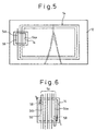
- An example of the plan profile of the plane coil 54 is shown in Fig. 5.
- the plane coil 54 is arranged so that a portion of the plane coil 54 can be arranged over the through-hole 14.
- the terminal sections 54a, 54b are also arranged over the through-hole 14.
- the terminal sections 54a, 54b may be plated with gold.
- the semiconductor element 56 is housed in the through-hole 14 in such a manner that the electrode terminal forming face is directed to the plane coil 54 side as shown in Fig. 3.
- the semiconductor element 56 is housed in the through-hole 14 while the semiconductor element 56 is being positioned so that a pair of electrode terminals 58 formed on the electrode terminal face can be contacted with the terminal sections 54a, 54b of the plane coil 54.
- the electrode terminals 58 of the semiconductor element 56 are electrically connected with the terminal sections 54a, 54b of the plane coil 54 by means of ultrasonic bonding.
- These over-sheets 62 are integrated with both faces of the core sheet 12 when they are heated and pressed by means of thermal press as shown in Fig. 4. In this way, the non-contact type IC card illustrated in Fig. 4 can be manufactured.
Abstract
Description
- The present invention relates to a non-contact type IC card composed in such a manner that over-sheets are attached onto the respective faces of a core-sheet to which a semiconductor element and a plane coil are attached.
- Referring to Fig. 9, an overall arrangement of a conventional non-contact
type IC card 50 will be explained below. - The
core sheet 52 is made of polyimide resin. - The
plane coil 54 is formed on one face of thecore sheet 52. Thesemiconductor element 56 is mounted on one face of thecore sheet 52 so that the face of thesemiconductor element 56 on which theelectrode terminals 58 are formed, that is, the electrode terminal formation face of thesemiconductor element 56 can be opposed to one face of thecore sheet 52. Theelectrode terminals 58 are electrically connected with therespective terminal sections plane coil 54. - The over-sheets 62, on one face of each of which an
adhesive sheet 60 is formed, are attached onto the respective faces of thecore sheet 52. These over-sheets 62 andcore sheet 52 are subjected to thermal pressing, so that they are integrally heated, pressed and formed into a single body. - However, the following problems occur in the above mentioned conventional non-contact type IC card. Since the
semiconductor element 56 is mounted on the surface of thecore sheet 52 and further theover-sheet 62 is put on thesemiconductor element 56, the thickness of the non-contact type IC card is increased. Further, irregularities are caused on the surface of the non-contacttype IC card 50 by thesemiconductor element 56 mounted on the surface of thecore sheet 52. - Furthermore, since the
core sheet 52 is made of expensive polyimide resin, the unit price of the non-contacttype IC card 50 is high. - The present invention is intended to solve the above problems. Accordingly, it is an object of the present invention to provide a non-contact type IC card which is thin and in which irregularities are seldom caused on the surface of non-contact type IC card.
- According to the present invention, there is provided a non-contact type IC card comprising: a core sheet made of resin and having first and second surfaces and a through-hole penetrating from the first surface to the second surface; a plane coil formed on the first surface of the core sheet, the plane coil having respective terminals located at a region in the hole; a semiconductor element accommodated in the hole, the semiconductor element having electrodes terminals electrically connected to the respective terminals of the plane coil; and a pair of over sheets, made of resin, for covering the first and second surfaces, respectively, to integrally cover the core sheet with the plane coil and the semiconductor element.
- Due to the above arrangement, the semiconductor element is accommodated or housed in the through-hole formed on the core-sheet. Therefore, the thickness of the non-contact type IC card can be reduced, and irregularities are seldom-caused on the surface of the non-contact type IC card.
- If the resin material is changed from polyimide resin to polyethylene resin which is less expensive than polyimide resin, the unit price of the product can be lowered.
- If the through-hole is filled with sealing material, the semiconductor element can be mechanically reinforced. Therefore, the mechanical strength of the non-contact type semiconductor element can be enhanced when a bending force or an impact is given to the non-contact type semiconductor element.
- The respective terminals can be transversely extending along the first surface of the core sheet over an opening of the hole. Otherwise, respective terminals can be extending into and terminated at the opening region of the hole.
- A thickness of the semiconductor element may be substantially the same or a little smaller than that of the core sheet, so that the semiconductor element can thus be accommodated in the hole within a range of thickness of the core sheet.
- Referring to the appended drawings, preferred embodiments of the non-contact type IC card of the present invention will be explained with reference to the accompanying drawings; in which:-
- Figs. 1 to 4 are schematic illustrations for explaining a manufacturing process of an embodiment of the non-contact type IC card of the present invention;
- Fig. 5 is a plan view for explaining a positional relation between the plane coil and the thorough-hole of the non-contact type IC card shown in Fig. 1;
- Fig. 6 is an enlarged view showing a portion close to the through-hole illustrated in Fig. 5;
- Fig. 7 is an enlarged view showing a portion close to the through-hole of the non-contact type IC card in which both terminal sections of the plane coil protrude into the through-hole;
- Fig. 8 is a schematic illustration for explaining another embodiment of the non-contact type IC card of the present invention; and
- Fig. 9 is a schematic illustration for explaining an example of the structure of a conventional non-contact type IC card known in the prior art.
-
- First, referring to Figs. 4 and 5, the structure of the non-contact
type IC card 10 is explained below. In this connection, like reference characters are used to indicate like parts in these views and the view showing the conventional example, and detailed explanations are omitted here. - The
core sheet 12 is made of resin material, and the through-hole 14 is formed in thecore sheet 12 so as to penetrate from the upper surface to the lower surface of the IC card. In this case, when thecore sheet 12 is made of polyethylene resin, such as PET, which is less expensive than polyimide resin, the manufacturing cost of the non-contacttype IC card 10 can be preferably reduced. - The
plane coil 54 is formed on one face of thecore sheet 12, that is, theplane coil 54 is formed on a lower face of thecore sheet 12 as shown in Fig. 4. Theplane coil 54 is made of metal such as aluminum or copper, and bothterminal sections plane coil 54 are arranged in the through-hole 14. To be more specific, in this embodiment, theterminal sections plane coil 54 are arranged over the through-hole 14, and at least portions of theterminal sections electrode terminals 58 of thesemiconductor element 56 are connected are plated with gold. - The
semiconductor element 56 is housed in the through-hole 14 from the other face side (the upper face side shown in Fig. 4) of thecore sheet 12 so that the face on which theelectrode terminals 58 are formed, that is, the electrode terminal formation face can be directed onto theplane coil 54 side, and a pair ofelectrode terminals 58 are electrically connected with theterminal sections plane coil 54 by means of ultrasonic bonding. - In this case, when a
thin semiconductor element 56, the thickness of which is approximately 50 µ, is used, thesemiconductor element 56 does not protrude from the surface of the commonly usedcore sheet 12 made of PET, the thickness of which is approximately 75 µ. Therefore, no protruding portion are formed on the surface of the non-contacttype IC card 10. Further the thickness of the non-contacttype IC card 10 can be reduced. In this connection, in order to prevent the occurrence of irregularities, it is preferable that the thickness of thecore sheet 12 and that of the semiconductor element 56 (the thickness of thesemiconductor element 56 including the electrode terminals 58) are made equal to each other. - On both faces of the
core sheet 12, in the through-hole 14 of which thesemiconductor element 56 is housed, a pair of over-sheets 62 made of resin, on one face of each of which anadhesive layer 60 is formed, are respectively arranged in such a manner that theadhesive layer 60 is located on thecore sheet 12 side. These over-sheets 62 are integrated with thecore sheet 12 when they are heated and pressed by means of thermal press. In the same manner as that of thecore sheet 12, it is preferable that theover-sheets 62 are made of polyethylene resin which is less expensive than polyimide resin. - Next, referring to Figs. 1 to 4, the manufacturing process of the non-contact
type IC card 10 will be explained below. - In the first process, the through-
hole 14 is formed on thecore sheet 12 as shown in Fig. 1. In this connection, the profile and size of the through-hole 14 are determined so that thesemiconductor element 56 can be housed in the through-hole 14 while consideration is given to the profile of thesemiconductor element 56. In order to prevent the formation of irregularities on the surface of the non-contact type IC card, the thickness of thecore sheet 12 is determined by giving consideration to the thickness of thesemiconductor element 56, that is, it is preferable that the thickness of thecore sheet 12 is the same as the thickness of thesemiconductor element 56. - In the second process, a layer of foil 16 of metal such as copper or aluminum is made to adhere onto one face of the
core sheet 12, that is, a layer of foil 16 of metal such as copper or aluminum is made to adhere onto a lower face shown in Fig. 1 as illustrated in Fig. 2. - In the third process, the layer of metallic foil 16 is etched in a predetermined pattern, so that the
plane coil 54 is formed on one face of thecore sheet 12. An example of the plan profile of theplane coil 54 is shown in Fig. 5. Theplane coil 54 is arranged so that a portion of theplane coil 54 can be arranged over the through-hole 14. Especially, in the case of theplane coil 54 of this embodiment, as shown in Fig. 6, theterminal sections hole 14. However, it is possible to adopt such a structure that theterminal sections hole 14 but are extended into the through-hole 14 as shown in Fig. 7. If necessary, theterminal sections - In the fourth process, the
semiconductor element 56 is housed in the through-hole 14 in such a manner that the electrode terminal forming face is directed to theplane coil 54 side as shown in Fig. 3. In this case, thesemiconductor element 56 is housed in the through-hole 14 while thesemiconductor element 56 is being positioned so that a pair ofelectrode terminals 58 formed on the electrode terminal face can be contacted with theterminal sections plane coil 54. Theelectrode terminals 58 of thesemiconductor element 56 are electrically connected with theterminal sections plane coil 54 by means of ultrasonic bonding. - In the fifth process, the
over-sheets 62 made of polyethylene resin, on only one face of which theadhesive layer 60 is formed, are made to adhere onto both faces of thecore sheet 12, in the through-hole 14 of which thesemiconductor element 56 is housed. These over-sheets 62 are integrated with both faces of thecore sheet 12 when they are heated and pressed by means of thermal press as shown in Fig. 4. In this way, the non-contact type IC card illustrated in Fig. 4 can be manufactured. - When a process in which the sealing material is filled in the through-
hole 14 is provided between the fourth and the fifth process, it becomes possible to manufacture the non-contacttype IC card 20 in which the periphery of thesemiconductor element 56 is reinforced by thesealing material 18 as shown in Fig. 8.
Claims (7)
- A non-contact type IC card comprising:a core-sheet, made of resin, having first and second surfaces and a through-hole penetrating from said first surface to said second surface;a plane coil formed on said first surface of the core-sheet, said plane coil having respective terminals located at an opening region in said through-hole;a semiconductor element accommodated in said hole, said semiconductor element having electrodes terminals electrically connected to said respective terminals of the plane coil;a pair of over-sheets, made of resin, for covering said first and second surfaces, respectively, to integrally cover said core-sheet with said plane coil and said semiconductor element.
- An IC card as set forth in claim 1, wherein said core-sheet is made of polyethylene resin.
- An IC card as set forth in claim 1 or 2, wherein said over-sheets are made of polyethylene resin.
- An IC card as set forth in any one of the preceding claims, wherein said hole is filled with a sealing material.
- An IC card as set forth in claim 1, wherein said respective terminals are transversely extended along said first surface of the core sheet and over an opening of said through-hole.
- An IC card as set forth in any one of the preceding claims, wherein said respective terminals are extending into and terminated at said opening region of the through-hole.
- An IC card as set forth in any one of the preceding claims, wherein the thickness of said semiconductor element is substantially the same as, or a little smaller than, that of said core sheet, so that said semiconductor element is accommodated in said through-hole within the thickness of said core-sheet.
Applications Claiming Priority (2)
| Application Number | Priority Date | Filing Date | Title |
|---|---|---|---|
| JP14177299A JP3517374B2 (en) | 1999-05-21 | 1999-05-21 | Method for manufacturing non-contact type IC card |
| JP14177299 | 1999-05-21 |
Publications (2)
| Publication Number | Publication Date |
|---|---|
| EP1054346A2 true EP1054346A2 (en) | 2000-11-22 |
| EP1054346A3 EP1054346A3 (en) | 2001-09-12 |
Family
ID=15299827
Family Applications (1)
| Application Number | Title | Priority Date | Filing Date |
|---|---|---|---|
| EP00304121A Withdrawn EP1054346A3 (en) | 1999-05-21 | 2000-05-16 | Non-contact chip card comprising a pair of covering sheets |
Country Status (4)
| Country | Link |
|---|---|
| US (2) | US20020030255A1 (en) |
| EP (1) | EP1054346A3 (en) |
| JP (1) | JP3517374B2 (en) |
| KR (1) | KR20010014925A (en) |
Cited By (4)
| Publication number | Priority date | Publication date | Assignee | Title |
|---|---|---|---|---|
| EP1302894A2 (en) * | 2001-10-12 | 2003-04-16 | Multitape GmbH | Contactless chipcard and manufacturing process |
| WO2009004139A2 (en) * | 2007-05-21 | 2009-01-08 | Fasver | Flexible adhesive label for security furnished with at least one contactless microcircuit for an official document |
| WO2013152840A1 (en) * | 2012-04-10 | 2013-10-17 | Smartrac Ip B.V. | Transponder layer and method for producing same |
| CN103366215A (en) * | 2012-04-05 | 2013-10-23 | 英飞凌科技股份有限公司 | Data carrier for contactless data transmission and method for producing the same |
Families Citing this family (6)
| Publication number | Priority date | Publication date | Assignee | Title |
|---|---|---|---|---|
| JP2003044818A (en) * | 2001-07-31 | 2003-02-14 | Toppan Forms Co Ltd | Method for manufacturing combination type ic card |
| KR20040024696A (en) * | 2002-09-16 | 2004-03-22 | 위영환 | Method for forming the RF antenna in PET sheet, Method for producing the Smart Card using the PET sheet and Smart card using of the Method |
| JP3866178B2 (en) * | 2002-10-08 | 2007-01-10 | 株式会社ルネサステクノロジ | IC card |
| JP2004185208A (en) * | 2002-12-02 | 2004-07-02 | Sony Corp | Ic card |
| JP4479209B2 (en) * | 2003-10-10 | 2010-06-09 | パナソニック株式会社 | Electronic circuit device, method for manufacturing the same, and apparatus for manufacturing electronic circuit device |
| US7259678B2 (en) * | 2003-12-08 | 2007-08-21 | 3M Innovative Properties Company | Durable radio frequency identification label and methods of manufacturing the same |
Family Cites Families (16)
| Publication number | Priority date | Publication date | Assignee | Title |
|---|---|---|---|---|
| JPS61201390A (en) * | 1985-03-04 | 1986-09-06 | Casio Comput Co Ltd | Ic card |
| JPH074995B2 (en) * | 1986-05-20 | 1995-01-25 | 株式会社東芝 | IC card and method of manufacturing the same |
| US5480842A (en) * | 1994-04-11 | 1996-01-02 | At&T Corp. | Method for fabricating thin, strong, and flexible die for smart cards |
| DE4431605C2 (en) * | 1994-09-05 | 1998-06-04 | Siemens Ag | Method for producing a chip card module for contactless chip cards |
| US5528222A (en) * | 1994-09-09 | 1996-06-18 | International Business Machines Corporation | Radio frequency circuit and memory in thin flexible package |
| US5952713A (en) * | 1994-12-27 | 1999-09-14 | Takahira; Kenichi | Non-contact type IC card |
| JP4015717B2 (en) * | 1995-06-29 | 2007-11-28 | 日立マクセル株式会社 | Information carrier manufacturing method |
| US5786626A (en) * | 1996-03-25 | 1998-07-28 | Ibm Corporation | Thin radio frequency transponder with leadframe antenna structure |
| FR2760113B1 (en) * | 1997-02-24 | 1999-06-04 | Gemplus Card Int | METHOD FOR MANUFACTURING A CONTACTLESS CARD WITH A COILED ANTENNA |
| JPH10242333A (en) * | 1997-03-01 | 1998-09-11 | Nitto Denko Corp | Semiconductor device and its manufacture |
| DE69819299T2 (en) * | 1997-06-23 | 2004-07-29 | Rohm Co. Ltd. | IC MODULE AND IC CARD |
| JPH1134562A (en) * | 1997-07-17 | 1999-02-09 | Tokin Corp | Non-contact card |
| FR2769441A1 (en) * | 1997-10-07 | 1999-04-09 | Philips Electronics Nv | CONTACTLESS ELECTRONIC CARD AND MANUFACTURING METHOD THEREOF |
| KR100293419B1 (en) * | 1998-08-10 | 2001-09-17 | 김양성 | Contact or contactless combined IC card and its manufacturing method |
| KR100284112B1 (en) * | 1998-11-07 | 2001-08-07 | 주동욱 | Contactless IC card with reduced thickness of card and its manufacturing method |
| KR100284111B1 (en) * | 1998-11-07 | 2001-08-07 | 주동욱 | Contactless IC card using conductive adhesive film and its manufacturing method |
-
1999
- 1999-05-21 JP JP14177299A patent/JP3517374B2/en not_active Expired - Fee Related
-
2000
- 2000-05-16 EP EP00304121A patent/EP1054346A3/en not_active Withdrawn
- 2000-05-18 US US09/573,505 patent/US20020030255A1/en not_active Abandoned
- 2000-05-18 KR KR1020000026606A patent/KR20010014925A/en not_active Application Discontinuation
-
2002
- 2002-11-01 US US10/285,624 patent/US20030057536A1/en not_active Abandoned
Non-Patent Citations (1)
| Title |
|---|
| None * |
Cited By (8)
| Publication number | Priority date | Publication date | Assignee | Title |
|---|---|---|---|---|
| EP1302894A2 (en) * | 2001-10-12 | 2003-04-16 | Multitape GmbH | Contactless chipcard and manufacturing process |
| EP1302894A3 (en) * | 2001-10-12 | 2003-10-29 | Multitape GmbH | Contactless chipcard and manufacturing process |
| WO2009004139A2 (en) * | 2007-05-21 | 2009-01-08 | Fasver | Flexible adhesive label for security furnished with at least one contactless microcircuit for an official document |
| WO2009004139A3 (en) * | 2007-05-21 | 2009-02-19 | Fasver | Flexible adhesive label for security furnished with at least one contactless microcircuit for an official document |
| CN103366215A (en) * | 2012-04-05 | 2013-10-23 | 英飞凌科技股份有限公司 | Data carrier for contactless data transmission and method for producing the same |
| CN103366215B (en) * | 2012-04-05 | 2016-08-03 | 英飞凌科技股份有限公司 | The data medium transmitted for contactless data and production method thereof |
| WO2013152840A1 (en) * | 2012-04-10 | 2013-10-17 | Smartrac Ip B.V. | Transponder layer and method for producing same |
| US9792543B2 (en) | 2012-04-10 | 2017-10-17 | Smartrac I.P. B.V. | Transponder layer and method for the production thereof |
Also Published As
| Publication number | Publication date |
|---|---|
| KR20010014925A (en) | 2001-02-26 |
| US20030057536A1 (en) | 2003-03-27 |
| JP3517374B2 (en) | 2004-04-12 |
| JP2000331138A (en) | 2000-11-30 |
| US20020030255A1 (en) | 2002-03-14 |
| EP1054346A3 (en) | 2001-09-12 |
Similar Documents
| Publication | Publication Date | Title |
|---|---|---|
| EP1514698B1 (en) | Card mounted with circuit chip and circuit chip module | |
| US6435415B1 (en) | Contactless electronic memory card | |
| JPH054483A (en) | Method for producing identification card provided with ic chip | |
| EP0854511A2 (en) | Resin sealing type semiconductor device | |
| AU2006252092B2 (en) | Card and manufacturing method | |
| US20120201994A1 (en) | Functional laminate | |
| EP1054346A2 (en) | Non-contact chip card comprising a pair of covering sheets | |
| JP2000182017A (en) | Ic card used as contacing/noncontacting type and its manufacture | |
| EP0886239B1 (en) | Wireless module and wireless card | |
| KR20000069487A (en) | Carrier element for a semiconductor chip for installing in chip cards | |
| US6380614B1 (en) | Non-contact type IC card and process for manufacturing same | |
| JP2844085B2 (en) | Circuit board and method of mounting semiconductor element | |
| US20040256150A1 (en) | Nonconducting substrate, forming a strip or a panel, on which a multiplicity of carrier elements are formed | |
| JP2000105810A (en) | Ic card, antenna for ic card, and antenna frame for ic card | |
| US6374486B1 (en) | Smart card and process for manufacturing the same | |
| KR101158128B1 (en) | Method for mounting an electronic component on a substrate | |
| US6255725B1 (en) | IC card and plane coil for IC card | |
| US20070170564A1 (en) | Chip card module | |
| CN1264480A (en) | Method for making contactless smart card | |
| EP1001364B1 (en) | Ic card and flat coil for ic card | |
| JP3382487B2 (en) | Non-contact IC card and method of manufacturing the same | |
| US7948764B2 (en) | Method for mounting an electronic component on a preferably soft support, and resulting electronic entity, such as a passport | |
| JP2001203296A (en) | Ic chip package board for ic card | |
| JP3764213B2 (en) | IC card and manufacturing method thereof | |
| KR20220013204A (en) | Metal card and manufacturing method thereof |
Legal Events
| Date | Code | Title | Description |
|---|---|---|---|
| PUAI | Public reference made under article 153(3) epc to a published international application that has entered the european phase |
Free format text: ORIGINAL CODE: 0009012 |
|
| AK | Designated contracting states |
Kind code of ref document: A2 Designated state(s): AT BE CH CY DE DK ES FI FR GB GR IE IT LI LU MC NL PT SE Kind code of ref document: A2 Designated state(s): DE FR GB |
|
| AX | Request for extension of the european patent |
Free format text: AL;LT;LV;MK;RO;SI |
|
| PUAL | Search report despatched |
Free format text: ORIGINAL CODE: 0009013 |
|
| AK | Designated contracting states |
Kind code of ref document: A3 Designated state(s): AT BE CH CY DE DK ES FI FR GB GR IE IT LI LU MC NL PT SE |
|
| AX | Request for extension of the european patent |
Free format text: AL;LT;LV;MK;RO;SI |
|
| 17P | Request for examination filed |
Effective date: 20020215 |
|
| AKX | Designation fees paid |
Free format text: DE FR GB |
|
| 17Q | First examination report despatched |
Effective date: 20061019 |
|
| STAA | Information on the status of an ep patent application or granted ep patent |
Free format text: STATUS: THE APPLICATION IS DEEMED TO BE WITHDRAWN |
|
| 18D | Application deemed to be withdrawn |
Effective date: 20070301 |