EP1052721B1 - Corrugated waveguide filter having coupled resonator cavities - Google Patents
Corrugated waveguide filter having coupled resonator cavities Download PDFInfo
- Publication number
- EP1052721B1 EP1052721B1 EP00109183A EP00109183A EP1052721B1 EP 1052721 B1 EP1052721 B1 EP 1052721B1 EP 00109183 A EP00109183 A EP 00109183A EP 00109183 A EP00109183 A EP 00109183A EP 1052721 B1 EP1052721 B1 EP 1052721B1
- Authority
- EP
- European Patent Office
- Prior art keywords
- filter
- pass
- resonator
- resonators
- waveguide
- Prior art date
- Legal status (The legal status is an assumption and is not a legal conclusion. Google has not performed a legal analysis and makes no representation as to the accuracy of the status listed.)
- Expired - Lifetime
Links
Images


Classifications
-
- H—ELECTRICITY
- H01—ELECTRIC ELEMENTS
- H01P—WAVEGUIDES; RESONATORS, LINES, OR OTHER DEVICES OF THE WAVEGUIDE TYPE
- H01P1/00—Auxiliary devices
- H01P1/20—Frequency-selective devices, e.g. filters
- H01P1/207—Hollow waveguide filters
- H01P1/211—Waffle-iron filters; Corrugated structures
Definitions
- the present invention is directed to the field of electronic filters. More particularly, the present invention provides a compact waveguide filter providing band-pass or low-pass response in the microwave frequency range.
- Waveguide filters are known in this art. There are two primary types of filters for use in the microwave frequency range (i.e. from about 2-20 GHz) -- symmetrically corrugated filters and iris filters. However, both of these types of filters suffer from many disadvantages.
- FIG. 1 of the '710 patent shows a standard E-plane corrugated structure having a uniform waveguide channel with a plurality of symmetrical corrugations. But as noted in the '710 patent, these types of corrugated filters are typically low-pass only. Such a filter typically cannot provide a band-pass response.
- the '710 patent purports to have advantages over the standard corrugated structure by forming a plurality of capacitive irises. Instead of forming a uniform waveguide channel, the '710 patent provides a series of iris structures ( Figs. 2 and 6 ), which have different heights. Although the irises and the corrugations are of different height, for any one iris or corrugation the structure is symmetrical.
- Another example of an iris filter (known as an H-plane iris filter) is shown in United States Patent No. 2,585,563 to Lewis, et al. This type of iris filter suffers from many disadvantages, however. First, it typically provides band-pass response only, i.e.
- the iris filter is typically a large structure, as the irises are generally separated along the waveguide channel by a half of a wavelength ( ⁇ g/2). Since the number of irises typically correlates to the order of the filter, when the order of the filter is high, such as 5th order or greater, the filter is very large.
- filters include resonant iris filters (as shown in United States Patent Nos. 1,788,538 to Norton and 1,849,659 to Bennett) and evanescent-mode ridged filters (as shown in United States Patent No. 4,646,039 to Saad).
- the resonant iris filter utilizes a plurality of resonant diaphragms as resonating elements that are separated by a quarter of a wavelength ( ⁇ g/4).
- the evanescent-mode ridged filter is based on a wavelength structure with a ridged cross section.
- a common problem with both of these types of filters is that they typically cannot handle high-powered signals.
- WO-A-00/55937 discloses a waveguide filter having asymmetrically corrugated resonators. Each resonator contributes one reflection zero and two transmission zeros to the frequency response of the filter. Each resonator has a pair of opposed slots which span the waveguide channel and are of different depths.
- US-A-3,597,710 discloses a waveguide band pass filter that has a series of capacitative irises that form corrugations within a rectangular waveguide.
- the irises provide a series of discontinuities but are not resonators.
- DE-A-19736367 discloses a waveguide having a series of cavities in the E-plane which do not act as resonators.
- a corrugated waveguide filter having a frequency response comprising a passband with a centre frequency
- the filter comprising: a plurality of resonators (64); and a plurality of coupling transformers (66) connecting said resonators, each coupling transformer (66) coupling respective two adjacent resonators; wherein each resonator (64) comprises a pair of extracted cavities separated by a distance (d), each of the two cavities comprising one slot (68A, 68B) with the same depth (h); wherein each resonator is operable to provide a reflection zero (76, 86) and a second order transmission zero (78, 88) to the frequency response of the filter, the reflection zero (76, 86) being within the filter passband and the second order transmission zero (78, 88) being either above or below the filter passband, and characterized in that : each coupling transformer (66) is a uniform waveguide section extending along the direction of said slots (68A, 68B) with a
- the present invention overcomes the disadvantages of presently known filters and also provides many advantages, such as: (1) compact size; (2) high-powered capability; (3) sharp roll-off on both sides of the pass-band; (4) low insertion loss; (5) wide and deep rejection response; (6) optional transformer units; and (7) either horizontal or vertical implementations.
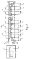
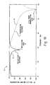
- FIG. 1 is an E-plane cross-section and end-view of a corrugated waveguide filter 10A according to the present invention having a plurality of symmetrical resonators 16A arranged in a horizontal manner.
- the filter 10A includes interface flanges 12, quarter-wave transformer sections 14, external waveguide connections 18, and a plurality of symmetrical resonators 16A.
- the interface flanges 12 connect the waveguide 10A to external waveguide line (not shown).
- the quarter-wave transformers 14 couple the external waveguide line to the internal portion of the filter, where the waveguide channel 15 is formed, and where the filtering takes place.
- the waveguide channel 15 provides a path for electromagnetic energy flow through the filter.
- each of the resonators 16A includes a pair of closely-spaced (i.e. much less than ⁇ g/4) corrugated cavities (or slots), thus forming a coupled resonator cavity 16A.
- the structure, spacing and configuration of these corrugated resonators 16A determines the frequency response of the filter.
- the resonators 16A in Figure 1 are symmetrical in the sense that the corrugated slots that form the resonator couple extend into both of the side walls of the waveguide channel 15. In the embodiment of the invention shown in Figure 2 , the resonators are asymmetrical since the corrugated slots extend into only one of the waveguide channel 15 side walls.
- the resonators are preferably separated ("y") by a quarter of a wavelength of the central frequency of the pass-band ( ⁇ g/4) of the filter, although they could be separated by a longer or shorter distance.
- the transformer sections 14 are also preferably ⁇ g/4 in length ("x"), although they could be of a different length. Each of the transformer sections 14 contributes a reflection zero to the frequency response of the filter
- Each of the resonators 16A provides a reflection zero within the pass-band of the filter, and also provides a second-order transmission zero (i.e. two transmission zeros) on either the high-side or low-side of the pass-band.
- the resonators 16A can be of two types -- low-pass or high-pass.
- the low-pass resonators have corrugated slots (or cavities) in which the depth of the cavities is less than ⁇ g/4, and the high-pass resonators have corrugated slots in which the depth of the cavities is greater than ⁇ g/4.
- the filter 10A shown in Figure 1 provides an Nth-order bandpass response, where N is the number of resonators 16A formed in the structure. If the transformer units 14 are utilized, then the order of the filter is N+2, as each transformer 14 contributes a reflection zero within the pass-band of the filter. Because each of the internal resonators 16A also provides second-order transmission zeros either below or above the pass-band, the roll-off at the edges of the pass-band is sharp and wide.
- the filter response can be designed to be of many types, including Chebychev or maximally-flat, for example.
- Figure 2 is an E-plane cross-section and end-view of another corrugated waveguide filter 10B according to the present invention having a plurality of asymmetrical resonators 16B arranged in a horizontal manner.
- the elements of the filter in Figure 2 are the same as in Figure 1 , except that the corrugations in the waveguide channel 15 are formed on only one side wall.
- the performance of this type of filter is slightly less than the filter shown in Figure 1 , it provides many of the same advantages since the coupled resonator pairs 16B operate in the same fashion as the coupled resonator pairs 16A in Figure 1 -- i.e . each resonator 16B contributes a reflection zero within the pass-band of the filter and two transmission zeros on one side of the pass-band.
- the waveguide filters 10A, 10B are preferably made of aluminum, although other materials could be used. In addition, these filters preferably operate in the microwave region between 2 and 20 GHz, however they could easily operate at other frequencies. The filters are particularly well-suited for high-powered microwave signals.
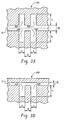
- Figure 3A is an E-plane cross-section of one of the symmetrical resonators 16A shown in Figure 1
- Figure 3B is the same for one of the asymmetrical resonators 16B shown in Figure 2
- the symmetrical resonator 16A includes a pair of extracted cavities.
- a first cavity having two extracted slots 20A, 20B, and a second cavity also having two extracted slots 20C, 20D.
- the two slots in a given cavity are separated by the waveguide channel 15, which has a dimension 2b.
- the width of the dimension 2b effects the power-handling capability of the filter.
- Each slot 20A, 20B, 20C, 20D has dimensions "h” and "s" where "h” is the depth of the slot and "s" is the width of the slot.
- the two cavities are, in turn, separated by a distance "d".
- the distance between the cavitites “d” determines the resonant frequency of the resonator couple, and hence the position of the reflection zero.
- the dimension “h” of the slots determines the position of the transmission zeros, either higher than or lower than the pass-band of the filter. If the dimension "h" is less than ⁇ g/4, then the transmission zeros an on the high-side of the pass-band, and therefore the resonator is a low-pass type. Alternately, if the dimension "h” is greater than ⁇ g/4, then the transmission zeros are on the low-side of the pass-band, and therefore the resonator is a high-pass type. For the high-pass type resonator, the distance “h” is typically between ⁇ g/4 and ⁇ g/2. The "s" dimension, as well as the "h” dimension, determine the loaded quality factor of the resonator.
- the resonator shown in Figure 3B includes two coupled cavities (or slots) 22A, 22B separated by a distance "d".
- This resonator 16B is asymmetrical in that the slots are extracted from only one side of the waveguide channel 15 sidewall.
- this resonator operates according to the same principles as that in Figure 3A .
- the distance "d” determines the location of the reflection zero within the pass-band of the filter
- the distance “h” determines the positioning of the transmission zeros (and hence whether the resonator is low-pass or high-pass)
- the distance "s" effects the loaded quality factor of the resonator.
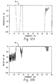
- Figures 4 , 5 , 6A, 6B , 7A and 7B are various simulation plots of the transmission and reflection response of a waveguide filter similar to the those set forth in Figures 1 and 2 .
- Figure 4 is a plot showing the transmission and reflection frequency response of a low-pass resonator for use with the waveguide filter.
- Figure 5 is the same for a high-pass resonator.
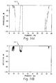
- Figures 6A and 6B are plots showing, respectively, the transmission and reflection frequency response of a filter such as shown in Figures 1 or 2 , in which the resonators are all low-pass.
- Figures 7A and 7B are plots showing, respectively, the transmission and reflection frequency response of a filter such as shown in Figures 1 or 2 , in which the resonators are both low-pass and high-pass.
- frequency is measured on the x-axis in GHz
- frequency response is measured on the y-axis in dB.
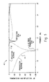
- FIG 4 a typical response 30 for a low-pass resonator is shown.
- the reflection response 32 and the transmission response 34 are graphed together in this plot.
- This type of resonator is characterized by a slot depth -- dimension "h" -- that is less than ⁇ g/4.
- the exact depth "h” determines the position of the second-order transmission zeros 38, which, as shown in the plot, are on the high-side of the passband, around 17.5 GHz.
- the position of the reflection zero 36 is at about 12 GHz -- within the pass-band of the filter -- and its exact location is determined by the distance "d" between the pair of coupled resonator slots.
- Figure 5 shows a similar response plot 40 for a high-pass resonator. Like Figure 4 , this plot shows the reflection response 42 and the transmission response 44.
- This type of resonator is characterized by a slot depth -- dimension "h" -- that is greater than ⁇ g/4.
- the exact depth "h” determines the position of the second-order transmission zeros 48, which, as shown in the plot, axe on the low-side of the passband, around 11 GHz.
- the position of the reflection zero 48 is at about 12 GHz -- within the pass-band of the filter -- and its exact location is determined by the distance "d" between the pair of coupled resonator slots in the high-pass resonator.
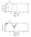
- Figures 6A and 6B set forth the transmission response 50 and reflection response 52 of a waveguide filter similar to those shown in Figure 1 or 2 , in which the resonators 16A or 16B are all of the low-pass type -- i.e "h" is less than ⁇ g/4 for each of the resonators.
- the roll-off on the low-side of the pass-band (which is between about 10.5 and 12.5 GHz) is less steep than on the high-side of the pass-band due to the multiple transmission zeros contributed by the low-pass resonators.
- Figure 8 is an E-plane cross-section of a corrugated waveguide filter 60 according to the present invention, including a plurality of H-stub resonators 64 arranged in a vertical manner.
- the input and output of the filter can be 1/4 wave transformer sections, similar to those shown in Figures 1 and 2 , or could be special T-shaped transformer sections 62 having an optional resonant iris element.
- Figure 8 shows a filter 60 with the T-shaped transformer sections 62. Between the transformers 62 are the plurality of H-stub resonators 64. Like Figures 1 and 2 , the number of resonators 64 determines the order of the filter. Each of the resonators 64 provides one reflection zero and a second-order transmission zero to the frequency response of the filter.
- This filter 60 can be used as a band-pass filter or a low-pass filter, depending on the configuration of the resonators and their positioning with respect to each other.
- Each of the resonators 64 is coupled together by a coupling transformer 66, which is a uniform (i.e. non-corrugated) waveguide section that is approximately ⁇ g/4 in length, although other distances are possible, including a distance of zero, in which case the resonators are just coupled together from one slot to the next.
- Quarter-wave coupling transformers 66 are used for implementations of the filter that are band-pass in order to achieve some rejection below the filter pass-band. For low-pass filter types, the coupling transformers 66 are reduced in length in order to provide more rejection on the high-side of the pass-band.
- Figure 9 is an E-plane cross-section of one of the H-stub resonators 64 shown in Figure 8 .
- the resonator 64 includes a pair of extracted cavities 68A, 68B, which are separated by a distance "d,” and connected on either side to the coupling transformers 66.
- the depth of the extracted cavities is denoted "h,” and the height of the section of waveguide coupling the resonators is denoted as "s.”
- the distance between the cavitites "d” determines the resonant frequency of the resonator couple, and hence the position of the reflection zero.
- the dimension "h” of the slots determines the position of the transmission zeros, either higher than or lower than the pass-band of the filter. If the dimension "h" is less than ⁇ g/4, then the transmission zeros are on the high-side of the pass-band, and therefore the resonator is a low-pass type. Alternately, if the dimension "h” is greater than ⁇ g/4, then the transmission zeros are on the low-side of the pass-band, and therefore the resonator is a high-pass type. For the high-pass type resonator, the distance “h” is typically between ⁇ g/4 and ⁇ g/2. The "s" dimension, as well as the "h” dimension, determine the loaded quality factor of the resonator.
- Figure 10 is a plot 70 showing the transmission and reflection frequency response of a low-pass H-stub resonator 64, and Figure 11 is the same 80 for a high-pass resonator.
- the reflection response 72 shows the positioning of the reflection zero 76 within the pass-band of the filter, around 12 GHz, and because this is a low-pass type resonator, the transmission response 74 shows the second order transmission zero 78 on the high side of the pass-band, around 17.5 GHz.
- the reflection response 82 shows the positioning of the reflection zero 86 within the pass-band of the filter, around 11.8 GHz
- the transmission response 84 shows the second order transmission zero 88 on the low side of the pass-band, around 10.9 GHz.
- the exact position of the reflection zeros is controlled by the resonator spacing "d,” and the exact position of the second order transmission zeros is controlled by the slot depth "h.”
- Figures 12A and 12B are plots showing, respectively, the transmission and reflection frequency response of a waveguide filter such as shown in Figure 8 , in which the resonators are low-pass H-stub type.
- the primary pass-band of this filter is between about 12.1 and 13.8 GHz, with a spurious pass-band below about 10 GHz. Because this filter is implemented with low-pass type resonators, the roll-off above the pass-band is typically sharper and the rejection of frequencies is deeper. Both of the pass-bands (primary and spurious) can be utilized for different applications, and if the coupling transformer sections 66 are reduced in length, then the primary pass-band will merge with the spurious pass-band resulting in a low-pass filter design. Alternatively, as described below, by using a special interface transformer with a resonant iris, the spurious pass-band can be attenuated.
- This low-pass filter design provides more rejection of high frequencies than a conventional corrugated filter using the same number of extracted cavities or irises.
- the present invention provides an improved low-pass filter that is very small and capable of handling high-powered signals.
- the insertion loss of a filter according to the present invention is lower than that for a typical corrugated design.
- Figure 13 is an E-plane cross-section of an interface transformer 62 for use with a waveguide filter such as shown in Figure 8 . If the filter structure and the interface to external waveguide lines have different cross-sections, or the direction of the input/output ports is to be altered, then the interface transformer 62 can be utilized. On one side of the transformer is the connection 104 to external waveguide, and the other side is a matching stub 102 that connects to the internal waveguide channel. Although Figure 13 shows a one-step transformer, other types could be utilized with larger numbers of steps between the external waveguide and the internal connection.
- the matching stub 102 provides an additional advantage in that it provides a transmission zero to the filter's frequency response, thus providing additional rejection.
- a resonant iris 100 can be used with the transformer 62 in order to provide attenuation of the spurious pass-band in the filter's frequency response.
- Figures 14A and 14B are plots 110, 112 showing, respectively, the transmission and reflection frequency response of a waveguide filter such as shown in Figure 8 , using the interface transformer 62 shown in Figure 13 . As compared to Figures 12A and 12B , these figures show the additional resection in the spurious pass-band provided by the transmission zero added by the interface transformer.
- Figures 15A and 15B are plots 114, 116 showing, respectively, the transmission and reflection frequency response of a waveguide filter such as shown in Figure 8 , using the interface transformer shown in Figure 13 with an optional resonant iris 100.
- the addition of the resonant iris 100 provides a great deal of suppression on the low-side of the pass-band, thus removing the spurious pass-band from the filter's frequency response.
Abstract
Description
- The present invention is directed to the field of electronic filters. More particularly, the present invention provides a compact waveguide filter providing band-pass or low-pass response in the microwave frequency range.
- Waveguide filters are known in this art. There are two primary types of filters for use in the microwave frequency range (i.e. from about 2-20 GHz) -- symmetrically corrugated filters and iris filters. However, both of these types of filters suffer from many disadvantages.
- An example of a symmetrically corrugated filter is shown in
United States Patent No. 3,597,710 to Levy ("the '710 patent").Figure 1 of the '710 patent shows a standard E-plane corrugated structure having a uniform waveguide channel with a plurality of symmetrical corrugations. But as noted in the '710 patent, these types of corrugated filters are typically low-pass only. Such a filter typically cannot provide a band-pass response. - The '710 patent purports to have advantages over the standard corrugated structure by forming a plurality of capacitive irises. Instead of forming a uniform waveguide channel, the '710 patent provides a series of iris structures (
Figs. 2 and6 ), which have different heights. Although the irises and the corrugations are of different height, for any one iris or corrugation the structure is symmetrical. Another example of an iris filter (known as an H-plane iris filter) is shown inUnited States Patent No. 2,585,563 to Lewis, et al. This type of iris filter suffers from many disadvantages, however. First, it typically provides band-pass response only, i.e., it is incapable of providing a combination response, such as low-pass and band-pass, or just a low-pass response. Secondly, the iris filter is typically a large structure, as the irises are generally separated along the waveguide channel by a half of a wavelength (λg/2). Since the number of irises typically correlates to the order of the filter, when the order of the filter is high, such as 5th order or greater, the filter is very large. - Other types of filters include resonant iris filters (as shown in
United States Patent Nos. 1,788,538 to Norton and1,849,659 to Bennett) and evanescent-mode ridged filters (as shown inUnited States Patent No. 4,646,039 to Saad). The resonant iris filter utilizes a plurality of resonant diaphragms as resonating elements that are separated by a quarter of a wavelength (λg/4). The evanescent-mode ridged filter is based on a wavelength structure with a ridged cross section. However, a common problem with both of these types of filters is that they typically cannot handle high-powered signals. - Therefore, there remains a general need in this field for a compact waveguide filter that provides multi-order band-pass or low-pass response, and is capable of handling high-powered signals in the GHz range.
-
WO-A-00/55937 -
US-A-3,597,710 discloses a waveguide band pass filter that has a series of capacitative irises that form corrugations within a rectangular waveguide. The irises provide a series of discontinuities but are not resonators. -
DE-A-19736367 discloses a waveguide having a series of cavities in the E-plane which do not act as resonators. - According to the invention, there is provided a corrugated waveguide filter having a frequency response comprising a passband with a centre frequency, the filter comprising: a plurality of resonators (64); and a plurality of coupling transformers (66) connecting said resonators, each coupling transformer (66) coupling respective two adjacent resonators; wherein each resonator (64) comprises a pair of extracted cavities separated by a distance (d), each of the two cavities comprising one slot (68A, 68B) with the same depth (h); wherein each resonator is operable to provide a reflection zero (76, 86) and a second order transmission zero (78, 88) to the frequency response of the filter, the reflection zero (76, 86) being within the filter passband and the second order transmission zero (78, 88) being either above or below the filter passband, and characterized in that: each coupling transformer (66) is a uniform waveguide section extending along the direction of said slots (68A, 68B) with a length of approximately a quarter of a wavelength of the centre frequency of the passband (λg/4).
- Preferably features are set out in the dependent claims.
- It should be noted that these are just some of the many aspects of the present invention. Other aspects not specified will become apparent upon reading the detailed description set forth below.
- The present invention overcomes the disadvantages of presently known filters and also provides many advantages, such as: (1) compact size; (2) high-powered capability; (3) sharp roll-off on both sides of the pass-band; (4) low insertion loss; (5) wide and deep rejection response; (6) optional transformer units; and (7) either horizontal or vertical implementations.
- These are just a few of the many advantages of the present invention, which is described in more detail below in terms of the preferred embodiments. As will be appreciated, the invention is capable of other and different embodiments, and its several details are capable of modifications in various respects. Accordingly, the drawings and description of the preferred embodiments set forth below are to be regarded as illustrative in nature and not restrictive.
- The present invention satisfies the general need noted above and provides many advantages, as will become apparent from the following description when read in conjunction with the accompanying drawings, wherein:
-
FIG. 1 is an E-plane cross-section and end-view of a corrugated waveguide filter according to the present invention having a plurality of symmetrical resonators arranged in a horizontal manner; -
FIG. 2 is an E-plane cross-section and end-view of another corrugated waveguide filter according to the present invention having a plurality of asymmetrical resonators arranged in a horizontal manner, -
FIG. 3A is an E-plane cross-section of one of the symmetrical resonators inFIG. 1 ; -
FIG. 3B is an E-plane cross-section of one of the asymmetrical resonators inFIG. 2 ; -
FIG. 4 is a plot showing the transmission and reflection frequency response of a low-pass resonator; -
FIG. 5 is a plot showing the transmission and reflection frequency response of a high-pass resonator; -
FIG. 6A is a plot showing the transmission frequency response of a filter such as shown inFIGs. 1 or2 , in which the resonators are all low-pass; -
FIG. 6B is a plot showing the reflection frequency response of a filter such as shown inFIGs. 1 or2 , in which the resonators are all low-pass; -
FIG. 7A is a plot showing the transmission frequency response of a filter such as shown inFIGs. 1 or2 , in which the resonators are both low-pass and high-pass; -
FIG. 7B is a plot showing the reflection frequency response of a filter such as shown inFIGs. 1 or2 , in which the resonators are both low-pass and high-pass; -
FIG. 8 is an E-plane cross-section of another corrugated waveguide filter according to the present invention, including a plurality of H-stub resonators arranged in a vertical manner; -
FIG. 9 is an E-plane cross-section of one of the H-stub resonators shown inFIG. 8 ; -
FIG. 10 is a plot showing the transmission and reflection frequency response of a low-pass H-stub resonator; -
FIG. 11 is a plot showing the transmission and reflection frequency response of a high-pass H-stub resonator; -
FIG. 12A is a plot showing the transmission frequency response of a waveguide filter such as shown inFIG. 8 , in which the resonators are low-pass H-stub type; -
FIG. 12B is a plot showing the reflection frequency response of a waveguide filter such as shown inFIG. 8 , in which the resonators are low-pass H-stub type; -
FIG. 13 is an E-plane cross-section of an interface transformer for use with a waveguide filter such as shown inFIG. 8 ; -
FIG. 14A is a plot showing the transmission frequency response of a waveguide filter such as shown inFIG. 8 , using the interface transformer shown inFIG. 13 ; -
FIG. 14B is a plot showing the reflection frequency response of a waveguide filter such as shown inFIG. 8 , using the interface transformer shown inFIG. 13 ; -
FIG. 15A is a plot showing the transmission frequency response of a waveguide filter such as shown inFIG. 8 , using the interface transformer shown inFIG. 13 with an optional resonant iris; and -
FIG. 15B is a plot showing the reflection frequency response of a waveguide filter such as shown inFIG. 8 , using the interface transformer shown inFIG. 13 with an optional resonant iris. - Turning now to the drawing figures,
Figure 1 is an E-plane cross-section and end-view of acorrugated waveguide filter 10A according to the present invention having a plurality ofsymmetrical resonators 16A arranged in a horizontal manner. Thefilter 10A includesinterface flanges 12, quarter-wave transformer sections 14,external waveguide connections 18, and a plurality ofsymmetrical resonators 16A. The interface flanges 12 connect thewaveguide 10A to external waveguide line (not shown). The quarter-wave transformers 14 couple the external waveguide line to the internal portion of the filter, where thewaveguide channel 15 is formed, and where the filtering takes place. Thewaveguide channel 15 provides a path for electromagnetic energy flow through the filter. Theresonators 16A are formed within the side walls of thewaveguide channel 15. As described in more detail below, each of theresonators 16A includes a pair of closely-spaced (i.e. much less than λg/4) corrugated cavities (or slots), thus forming a coupledresonator cavity 16A. The structure, spacing and configuration of thesecorrugated resonators 16A determines the frequency response of the filter. - The
resonators 16A inFigure 1 are symmetrical in the sense that the corrugated slots that form the resonator couple extend into both of the side walls of thewaveguide channel 15. In the embodiment of the invention shown inFigure 2 , the resonators are asymmetrical since the corrugated slots extend into only one of thewaveguide channel 15 side walls. The resonators are preferably separated ("y") by a quarter of a wavelength of the central frequency of the pass-band (λg/4) of the filter, although they could be separated by a longer or shorter distance. Thetransformer sections 14 are also preferably λg/4 in length ("x"), although they could be of a different length. Each of thetransformer sections 14 contributes a reflection zero to the frequency response of the filter - Each of the
resonators 16A provides a reflection zero within the pass-band of the filter, and also provides a second-order transmission zero (i.e. two transmission zeros) on either the high-side or low-side of the pass-band. Theresonators 16A can be of two types -- low-pass or high-pass. The low-pass resonators have corrugated slots (or cavities) in which the depth of the cavities is less than λg/4, and the high-pass resonators have corrugated slots in which the depth of the cavities is greater than λg/4. - The
filter 10A shown inFigure 1 provides an Nth-order bandpass response, where N is the number ofresonators 16A formed in the structure. If thetransformer units 14 are utilized, then the order of the filter is N+2, as eachtransformer 14 contributes a reflection zero within the pass-band of the filter. Because each of theinternal resonators 16A also provides second-order transmission zeros either below or above the pass-band, the roll-off at the edges of the pass-band is sharp and wide. The filter response can be designed to be of many types, including Chebychev or maximally-flat, for example. -
Figure 2 is an E-plane cross-section and end-view of anothercorrugated waveguide filter 10B according to the present invention having a plurality ofasymmetrical resonators 16B arranged in a horizontal manner. The elements of the filter inFigure 2 are the same as inFigure 1 , except that the corrugations in thewaveguide channel 15 are formed on only one side wall. Although the performance of this type of filter is slightly less than the filter shown inFigure 1 , it provides many of the same advantages since the coupled resonator pairs 16B operate in the same fashion as the coupled resonator pairs 16A inFigure 1 -- i.e. eachresonator 16B contributes a reflection zero within the pass-band of the filter and two transmission zeros on one side of the pass-band. - The waveguide filters 10A, 10B are preferably made of aluminum, although other materials could be used. In addition, these filters preferably operate in the microwave region between 2 and 20 GHz, however they could easily operate at other frequencies. The filters are particularly well-suited for high-powered microwave signals.
-
Figure 3A is an E-plane cross-section of one of thesymmetrical resonators 16A shown inFigure 1 , andFigure 3B is the same for one of theasymmetrical resonators 16B shown inFigure 2 . Thesymmetrical resonator 16A includes a pair of extracted cavities. A first cavity having two extractedslots waveguide channel 15, which has adimension 2b. The width of thedimension 2b effects the power-handling capability of the filter. Eachslot - The distance between the cavitites "d" determines the resonant frequency of the resonator couple, and hence the position of the reflection zero. The dimension "h" of the slots determines the position of the transmission zeros, either higher than or lower than the pass-band of the filter. If the dimension "h" is less than λg/4, then the transmission zeros an on the high-side of the pass-band, and therefore the resonator is a low-pass type. Alternately, if the dimension "h" is greater than λg/4, then the transmission zeros are on the low-side of the pass-band, and therefore the resonator is a high-pass type. For the high-pass type resonator, the distance "h" is typically between λg/4 and λg/2. The "s" dimension, as well as the "h" dimension, determine the loaded quality factor of the resonator.
- Like
Figure 3A , the resonator shown inFigure 3B includes two coupled cavities (or slots) 22A, 22B separated by a distance "d". Thisresonator 16B is asymmetrical in that the slots are extracted from only one side of thewaveguide channel 15 sidewall. Other than a slight difference in performance, this resonator operates according to the same principles as that inFigure 3A . The distance "d" determines the location of the reflection zero within the pass-band of the filter, the distance "h" determines the positioning of the transmission zeros (and hence whether the resonator is low-pass or high-pass), and the distance "s" effects the loaded quality factor of the resonator. -
Figures 4 ,5 ,6A, 6B ,7A and 7B are various simulation plots of the transmission and reflection response of a waveguide filter similar to the those set forth inFigures 1 and2 . Specifically,Figure 4 is a plot showing the transmission and reflection frequency response of a low-pass resonator for use with the waveguide filter.Figure 5 is the same for a high-pass resonator.Figures 6A and 6B are plots showing, respectively, the transmission and reflection frequency response of a filter such as shown inFigures 1 or2 , in which the resonators are all low-pass. AndFigures 7A and 7B are plots showing, respectively, the transmission and reflection frequency response of a filter such as shown inFigures 1 or2 , in which the resonators are both low-pass and high-pass. In all these simulation plots, frequency is measured on the x-axis in GHz, and frequency response (either transmission or reflection) is measured on the y-axis in dB. - Turning first to
Figure 4 , atypical response 30 for a low-pass resonator is shown. Thereflection response 32 and thetransmission response 34 are graphed together in this plot. This type of resonator is characterized by a slot depth -- dimension "h" -- that is less than λg/4. The exact depth "h" determines the position of the second-order transmission zeros 38, which, as shown in the plot, are on the high-side of the passband, around 17.5 GHz. The position of the reflection zero 36 is at about 12 GHz -- within the pass-band of the filter -- and its exact location is determined by the distance "d" between the pair of coupled resonator slots. -
Figure 5 shows asimilar response plot 40 for a high-pass resonator. LikeFigure 4 , this plot shows the reflection response 42 and thetransmission response 44. This type of resonator is characterized by a slot depth -- dimension "h" -- that is greater than λg/4. The exact depth "h" determines the position of the second-order transmission zeros 48, which, as shown in the plot, axe on the low-side of the passband, around 11 GHz. The position of the reflection zero 48 is at about 12 GHz -- within the pass-band of the filter -- and its exact location is determined by the distance "d" between the pair of coupled resonator slots in the high-pass resonator. -
Figures 6A and 6B set forth thetransmission response 50 andreflection response 52 of a waveguide filter similar to those shown inFigure 1 or2 , in which theresonators transmission plot 50 for this type of filter, the roll-off on the low-side of the pass-band (which is between about 10.5 and 12.5 GHz) is less steep than on the high-side of the pass-band due to the multiple transmission zeros contributed by the low-pass resonators. In order to make the filter's performance more symmetrical, high-pass resonator elements can be added to the filter, thus resulting in afrequency response Figures 7A and 7B , where the roll-off on either side of the pass-band is roughly the same. - The remaining drawing figures describe another embodiment of the present invention in which the coupled resonator cavities are arranged in a vertical implementation. The primary advantage of this implementation over
Figures 1 or2 (the horizontal configurations) is that it is very small in size. -
Figure 8 is an E-plane cross-section of acorrugated waveguide filter 60 according to the present invention, including a plurality of H-stub resonators 64 arranged in a vertical manner. The input and output of the filter can be 1/4 wave transformer sections, similar to those shown inFigures 1 and2 , or could be special T-shapedtransformer sections 62 having an optional resonant iris element.Figure 8 shows afilter 60 with the T-shapedtransformer sections 62. Between thetransformers 62 are the plurality of H-stub resonators 64. LikeFigures 1 and2 , the number ofresonators 64 determines the order of the filter. Each of theresonators 64 provides one reflection zero and a second-order transmission zero to the frequency response of the filter. Thisfilter 60 can be used as a band-pass filter or a low-pass filter, depending on the configuration of the resonators and their positioning with respect to each other. - Each of the
resonators 64 is coupled together by acoupling transformer 66, which is a uniform (i.e. non-corrugated) waveguide section that is approximately λg/4 in length, although other distances are possible, including a distance of zero, in which case the resonators are just coupled together from one slot to the next. Quarter-wave coupling transformers 66 are used for implementations of the filter that are band-pass in order to achieve some rejection below the filter pass-band. For low-pass filter types, thecoupling transformers 66 are reduced in length in order to provide more rejection on the high-side of the pass-band. -
Figure 9 is an E-plane cross-section of one of the H-stub resonators 64 shown inFigure 8 . Theresonator 64 includes a pair of extractedcavities coupling transformers 66. The depth of the extracted cavities is denoted "h," and the height of the section of waveguide coupling the resonators is denoted as "s." Similar to theresonators -
Figure 10 is aplot 70 showing the transmission and reflection frequency response of a low-pass H-stub resonator 64, andFigure 11 is the same 80 for a high-pass resonator. Turning first toFigure 10 , thereflection response 72 shows the positioning of the reflection zero 76 within the pass-band of the filter, around 12 GHz, and because this is a low-pass type resonator, thetransmission response 74 shows the second order transmission zero 78 on the high side of the pass-band, around 17.5 GHz. Likewise for the high-pass resonator inFigure 11 , thereflection response 82 shows the positioning of the reflection zero 86 within the pass-band of the filter, around 11.8 GHz, and thetransmission response 84 shows the second order transmission zero 88 on the low side of the pass-band, around 10.9 GHz. As noted above, the exact position of the reflection zeros is controlled by the resonator spacing "d," and the exact position of the second order transmission zeros is controlled by the slot depth "h." -
Figures 12A and 12B are plots showing, respectively, the transmission and reflection frequency response of a waveguide filter such as shown inFigure 8 , in which the resonators are low-pass H-stub type. As shown in these figures, the primary pass-band of this filter is between about 12.1 and 13.8 GHz, with a spurious pass-band below about 10 GHz. Because this filter is implemented with low-pass type resonators, the roll-off above the pass-band is typically sharper and the rejection of frequencies is deeper. Both of the pass-bands (primary and spurious) can be utilized for different applications, and if thecoupling transformer sections 66 are reduced in length, then the primary pass-band will merge with the spurious pass-band resulting in a low-pass filter design. Alternatively, as described below, by using a special interface transformer with a resonant iris, the spurious pass-band can be attenuated. - This low-pass filter design provides more rejection of high frequencies than a conventional corrugated filter using the same number of extracted cavities or irises. Thus, the present invention provides an improved low-pass filter that is very small and capable of handling high-powered signals. In addition, the insertion loss of a filter according to the present invention is lower than that for a typical corrugated design.
-
Figure 13 is an E-plane cross-section of aninterface transformer 62 for use with a waveguide filter such as shown inFigure 8 . If the filter structure and the interface to external waveguide lines have different cross-sections, or the direction of the input/output ports is to be altered, then theinterface transformer 62 can be utilized. On one side of the transformer is theconnection 104 to external waveguide, and the other side is a matchingstub 102 that connects to the internal waveguide channel. AlthoughFigure 13 shows a one-step transformer, other types could be utilized with larger numbers of steps between the external waveguide and the internal connection. The matchingstub 102 provides an additional advantage in that it provides a transmission zero to the filter's frequency response, thus providing additional rejection. Optionally, aresonant iris 100 can be used with thetransformer 62 in order to provide attenuation of the spurious pass-band in the filter's frequency response. -
Figures 14A and 14B areplots Figure 8 , using theinterface transformer 62 shown inFigure 13 . As compared toFigures 12A and 12B , these figures show the additional resection in the spurious pass-band provided by the transmission zero added by the interface transformer. -
Figures 15A and 15B areplots Figure 8 , using the interface transformer shown inFigure 13 with an optionalresonant iris 100. As seen in these plots, the addition of theresonant iris 100 provides a great deal of suppression on the low-side of the pass-band, thus removing the spurious pass-band from the filter's frequency response.
Claims (14)
- A corrugated waveguide filter having a frequency response comprising a passband with a centre frequency, the filter comprising:a plurality of resonators (64); anda plurality of coupling transformers (66) connecting said resonators, each coupling transformer (66) coupling respective two adjacent resonators;wherein each resonator (64) comprises a pair of extracted cavities separated by a distance (d), each of the two cavities comprising one slot (68A, 68B) with the same depth (h);
wherein each resonator is operable to provide a reflection zero (76, 86) and a second order transmission zero (78, 88) to the frequency response of the filter, the reflection zero (76, 86) being within the filter passband and the second order transmission zero (78, 88) being either above or below the filter passband, and
characterized in that:each coupling transformer (66) is a uniform waveguide section extending along the direction of said slots (68A, 68B) with a length of approximately a quarter of a wavelength of the centre frequency of the passband (λg/4). - The filter of claim 1, further comprising:an input transformer section (62); andan output transformer section (62);wherein the input and output transformer sections couple the waveguide filter to external waveguide lines.
- The filter of claim 2, wherein each transformer section (62) is operable to provide a reflection zero to the frequency response of the filter, the reflection zero being within the filter passband.
- The filter of claim 2, wherein one of the input transformer section (62) or the output transformer (62) section includes a resonant iris.
- The filter of claim 1, wherein the distance (d) between the cavities in a particular resonator determines the position of the reflection zero for that resonator.
- The filter of claim 1, wherein the depth (h) of the slots in a particular resonator determines the position of the second order transmission zero for that resonator.
- The filter of claim 6, wherein a particular resonator is a high-pass resonator if the depth (h) of the slots is greater than one-quarter of a wavelength of the centre frequency of the passband (λg/4) of the filter.
- The filter of claim 6, wherein a particular resonator is a low-pass resonator if the depth (h) of the slots is less than one-quarter of a wavelength of the centre frequency of the passband (λg/4) of the filter.
- The filter of claim 1, wherein the resonators are all low-pass resonators.
- The filter of claim 1, wherein the filter comprises at least one low-pass resonator and at least one high-pass resonator.
- The filter of claim 1, wherein the filter is made of aluminum.
- The filter of claim 1, wherein the filter operates between about 2 and 20 GHz.
- The filter of claim 1, wherein the resonators are H-stub resonators (64).
- The filter of claim 1, wherein the order of the filter bandpass response is determined by the number of resonators.
Applications Claiming Priority (2)
| Application Number | Priority Date | Filing Date | Title |
|---|---|---|---|
| US09/309,406 US6169466B1 (en) | 1999-05-10 | 1999-05-10 | Corrugated waveguide filter having coupled resonator cavities |
| US309406 | 1999-05-10 |
Publications (3)
| Publication Number | Publication Date |
|---|---|
| EP1052721A2 EP1052721A2 (en) | 2000-11-15 |
| EP1052721A3 EP1052721A3 (en) | 2002-03-06 |
| EP1052721B1 true EP1052721B1 (en) | 2010-04-28 |
Family
ID=23198106
Family Applications (1)
| Application Number | Title | Priority Date | Filing Date |
|---|---|---|---|
| EP00109183A Expired - Lifetime EP1052721B1 (en) | 1999-05-10 | 2000-05-08 | Corrugated waveguide filter having coupled resonator cavities |
Country Status (4)
| Country | Link |
|---|---|
| US (1) | US6169466B1 (en) |
| EP (1) | EP1052721B1 (en) |
| AT (1) | ATE466388T1 (en) |
| DE (1) | DE60044274D1 (en) |
Cited By (1)
| Publication number | Priority date | Publication date | Assignee | Title |
|---|---|---|---|---|
| WO2014039819A1 (en) * | 2012-09-07 | 2014-03-13 | Bridgewave Communications, Inc. | Metalized plastic components for millimeter wave electronics |
Families Citing this family (15)
| Publication number | Priority date | Publication date | Assignee | Title |
|---|---|---|---|---|
| DE19736367A1 (en) * | 1997-08-21 | 1999-02-25 | Bosch Gmbh Robert | Waveguide filter for HF power amplifier |
| US6917266B2 (en) * | 2000-10-11 | 2005-07-12 | Paul Mack | Microwave waveguide |
| US7132909B2 (en) * | 2000-10-11 | 2006-11-07 | Paul Mack | Microwave waveguide |
| JP4173679B2 (en) * | 2002-04-09 | 2008-10-29 | エム・イー・エス・アフティ株式会社 | ECR plasma source and ECR plasma apparatus |
| FR2848342A1 (en) * | 2002-12-09 | 2004-06-11 | Thomson Licensing Sa | Pass-band filter with pseudo-elliptical response of wave guide type has floating insert inside one inductive iris |
| US7606592B2 (en) * | 2005-09-19 | 2009-10-20 | Becker Charles D | Waveguide-based wireless distribution system and method of operation |
| CN103700908B (en) * | 2013-12-09 | 2016-05-11 | 成都九洲迪飞科技有限责任公司 | Ultra broadband waveguide filter |
| MX2017010030A (en) * | 2015-03-01 | 2017-10-27 | ERICSSON TELEFON AB L M (publ) | Waveguide e-plane filter. |
| CN105680123B (en) * | 2016-01-11 | 2018-05-25 | 中国电子科技集团公司第十研究所 | EHF frequency range millimeter wave cut-off waveguide bandpass filters |
| KR102640203B1 (en) * | 2016-06-24 | 2024-02-23 | 삼성전자주식회사 | Optical device including slot and apparatus employing the optical device |
| US11199661B2 (en) | 2019-10-21 | 2021-12-14 | Honeywell International Inc. | Integrated photonics vertical coupler |
| US11079542B2 (en) | 2019-10-21 | 2021-08-03 | Honeywell International Inc. | Integrated photonics source and detector of entangled photons |
| US11320720B2 (en) | 2019-10-21 | 2022-05-03 | Honeywell International Inc. | Integrated photonics mode splitter and converter |
| CN113054375A (en) * | 2019-12-27 | 2021-06-29 | 深圳市大富科技股份有限公司 | Communication device and filter thereof |
| CN115000659B (en) * | 2022-06-17 | 2022-12-16 | 华南理工大学 | Waveguide filter based on resonant coupling structure |
Citations (2)
| Publication number | Priority date | Publication date | Assignee | Title |
|---|---|---|---|---|
| US3597710A (en) * | 1969-11-28 | 1971-08-03 | Microwave Dev Lab Inc | Aperiodic tapered corrugated waveguide filter |
| WO2000055937A1 (en) * | 1999-03-12 | 2000-09-21 | Com Dev Limited | Waveguide filter having asymmetrically corrugated resonators |
Family Cites Families (28)
| Publication number | Priority date | Publication date | Assignee | Title |
|---|---|---|---|---|
| US1788538A (en) | 1929-04-16 | 1931-01-13 | Bell Telephone Labor Inc | Filtering circuits |
| US1849656A (en) | 1929-06-29 | 1932-03-15 | Bell Telephone Labor Inc | Transmission network |
| US2540488A (en) | 1948-04-30 | 1951-02-06 | Bell Telephone Labor Inc | Microwave filter |
| US2585563A (en) | 1949-09-17 | 1952-02-12 | Bell Telephone Labor Inc | Wave filter |
| US3046503A (en) | 1960-05-27 | 1962-07-24 | Seymour B Cohn | Broad-band waveguide filter |
| US3271706A (en) | 1964-12-07 | 1966-09-06 | Gen Electric | Microwave filter |
| GB1136158A (en) | 1966-06-10 | 1968-12-11 | Standard Telephones Cables Ltd | Improvements in or relating to waveguide filters |
| GB1129185A (en) | 1966-06-10 | 1968-10-02 | Standard Telephones Cables Ltd | Improvements in or relating to waveguide filters |
| US3634788A (en) | 1967-09-27 | 1972-01-11 | Int Standard Electric Corp | Waveguide filter |
| US3611214A (en) * | 1969-08-18 | 1971-10-05 | Varian Associates | Waveguide reflective harmonic filter |
| US3819900A (en) | 1972-06-13 | 1974-06-25 | Amana Refrigeration Inc | Waveguide filter for microwave heating apparatus |
| US3838368A (en) | 1972-06-13 | 1974-09-24 | Amana Refrigeration Inc | Waveguide filter for microwave heating apparatus |
| US3949327A (en) | 1974-08-01 | 1976-04-06 | Sage Laboratories, Inc. | Waveguide low pass filter |
| US4155056A (en) | 1977-08-25 | 1979-05-15 | Bell Telephone Laboratories, Incorporated | Cascaded grating resonator filters with external input-output couplers |
| US4492020A (en) | 1982-09-02 | 1985-01-08 | Hughes Aircraft Company | Method for fabricating corrugated microwave components |
| CA1193679A (en) | 1984-05-28 | 1985-09-17 | Abdelmegid K. Saad | Evanescent mode triple ridge lowpass harmonic filter |
| CA1194159A (en) | 1984-05-28 | 1985-09-24 | Abdelmegid K. Saad | Low pass filters with finite transmission zeros in evanescent modes |
| JPS6179301A (en) | 1984-09-27 | 1986-04-22 | Nec Corp | Band-pass filter of dielectric resonator |
| US4749973A (en) | 1985-06-20 | 1988-06-07 | Hitachi Heating Appliances Co., Ltd. | Waveguide filter used in a microwave oven |
| JPH02190001A (en) * | 1989-01-18 | 1990-07-26 | Nec Corp | Corrugate filter |
| US5004993A (en) | 1989-09-19 | 1991-04-02 | The United States Of America As Represented By The Secretary Of The Navy | Constricted split block waveguide low pass filter with printed circuit filter substrate |
| US5243618A (en) | 1991-11-22 | 1993-09-07 | Hughes Aircraft Company | Cavity resonator incorporating waveguide filter |
| US5381596A (en) | 1993-02-23 | 1995-01-17 | E-Systems, Inc. | Apparatus and method of manufacturing a 3-dimensional waveguide |
| US5357591A (en) | 1993-04-06 | 1994-10-18 | Yuan Jiang | Cylindrical-wave controlling, generating and guiding devices |
| US5598300A (en) | 1995-06-05 | 1997-01-28 | Board Of Regents, The University Of Texas System | Efficient bandpass reflection and transmission filters with low sidebands based on guided-mode resonance effects |
| US5600740A (en) | 1995-06-20 | 1997-02-04 | Asfar; Omar R. | Narrowband waveguide filter |
| US5715271A (en) | 1996-08-01 | 1998-02-03 | Northern Telecom Limited | Polarization independent grating resonator filter |
| DE19736367A1 (en) * | 1997-08-21 | 1999-02-25 | Bosch Gmbh Robert | Waveguide filter for HF power amplifier |
-
1999
- 1999-05-10 US US09/309,406 patent/US6169466B1/en not_active Expired - Lifetime
-
2000
- 2000-05-08 EP EP00109183A patent/EP1052721B1/en not_active Expired - Lifetime
- 2000-05-08 AT AT00109183T patent/ATE466388T1/en not_active IP Right Cessation
- 2000-05-08 DE DE60044274T patent/DE60044274D1/en not_active Expired - Lifetime
Patent Citations (3)
| Publication number | Priority date | Publication date | Assignee | Title |
|---|---|---|---|---|
| US3597710A (en) * | 1969-11-28 | 1971-08-03 | Microwave Dev Lab Inc | Aperiodic tapered corrugated waveguide filter |
| WO2000055937A1 (en) * | 1999-03-12 | 2000-09-21 | Com Dev Limited | Waveguide filter having asymmetrically corrugated resonators |
| US6232853B1 (en) * | 1999-03-12 | 2001-05-15 | Com Dev Limited | Waveguide filter having asymmetrically corrugated resonators |
Cited By (1)
| Publication number | Priority date | Publication date | Assignee | Title |
|---|---|---|---|---|
| WO2014039819A1 (en) * | 2012-09-07 | 2014-03-13 | Bridgewave Communications, Inc. | Metalized plastic components for millimeter wave electronics |
Also Published As
| Publication number | Publication date |
|---|---|
| ATE466388T1 (en) | 2010-05-15 |
| EP1052721A2 (en) | 2000-11-15 |
| US6169466B1 (en) | 2001-01-02 |
| EP1052721A3 (en) | 2002-03-06 |
| DE60044274D1 (en) | 2010-06-10 |
Similar Documents
| Publication | Publication Date | Title |
|---|---|---|
| EP1052721B1 (en) | Corrugated waveguide filter having coupled resonator cavities | |
| US4837535A (en) | Resonant wave filter | |
| US6411181B1 (en) | Dielectric resonator, inductor, capacitor, dielectric filter, oscillator, and communication device | |
| EP1161775B1 (en) | Waveguide filter having asymmetrically corrugated resonators | |
| US11031664B2 (en) | Waveguide band-pass filter | |
| EP0840390A1 (en) | Multi-passband filter | |
| JP2003508948A (en) | High frequency band filter device with transmission zero point | |
| WO2012004818A1 (en) | Waveguide band-pass filter with pseudo-elliptic response | |
| US6445263B1 (en) | Dielectric resonator, dielectric filter, duplexer, and communication device | |
| US6504456B2 (en) | Communication device having a spurious wave blocking circuit formed of a plural fundamental pattern | |
| US5739734A (en) | Evanescent mode band reject filters and related methods | |
| CN112563701B (en) | Dual-mode substrate integrated waveguide filter based on perturbation rectangular cavity | |
| JP2002084101A (en) | Filter, multiplexer, and communicating device | |
| JP2641090B2 (en) | Dual mode cavity resonator for waveguide bandpass filter | |
| EP0328747B1 (en) | Mode selective band pass filter | |
| US6104262A (en) | Ridged thick walled capacitive slot | |
| JPH01152801A (en) | Waveguide band-pass filter | |
| CA1050127A (en) | Low insertion loss waveguide filter | |
| US20230155267A1 (en) | Metallized dielectric waveguide filters having irregular shaped resonant cavities, slanted metallized openings and/or spurious coupling windows | |
| CA1081808A (en) | Dual mode self-equalized bandpass filters | |
| JPH11312902A (en) | Dielectric filter, transmission/reception equipment and communication equipment | |
| CN113036385B (en) | Three-path filtering power divider with high selectivity | |
| JPH0715210A (en) | Band-stop filter | |
| CA2298479C (en) | Spiral slot line resonator | |
| JPH0614601B2 (en) | Bandpass filter |
Legal Events
| Date | Code | Title | Description |
|---|---|---|---|
| PUAI | Public reference made under article 153(3) epc to a published international application that has entered the european phase |
Free format text: ORIGINAL CODE: 0009012 |
|
| 17P | Request for examination filed |
Effective date: 20000509 |
|
| AK | Designated contracting states |
Kind code of ref document: A2 Designated state(s): AT BE CH CY DE DK ES FI FR GB GR IE IT LI LU MC NL PT SE |
|
| AX | Request for extension of the european patent |
Free format text: AL;LT;LV;MK;RO;SI |
|
| PUAL | Search report despatched |
Free format text: ORIGINAL CODE: 0009013 |
|
| AK | Designated contracting states |
Kind code of ref document: A3 Designated state(s): AT BE CH CY DE DK ES FI FR GB GR IE IT LI LU MC NL PT SE |
|
| AX | Request for extension of the european patent |
Free format text: AL;LT;LV;MK;RO;SI |
|
| AKX | Designation fees paid |
Free format text: AT BE CH CY DE DK ES FI FR GB GR IE IT LI LU MC NL PT SE |
|
| 17Q | First examination report despatched |
Effective date: 20071113 |
|
| GRAP | Despatch of communication of intention to grant a patent |
Free format text: ORIGINAL CODE: EPIDOSNIGR1 |
|
| GRAS | Grant fee paid |
Free format text: ORIGINAL CODE: EPIDOSNIGR3 |
|
| GRAA | (expected) grant |
Free format text: ORIGINAL CODE: 0009210 |
|
| AK | Designated contracting states |
Kind code of ref document: B1 Designated state(s): AT BE CH CY DE DK ES FI FR GB GR IE IT LI LU MC NL PT SE |
|
| REG | Reference to a national code |
Ref country code: GB Ref legal event code: FG4D |
|
| REG | Reference to a national code |
Ref country code: CH Ref legal event code: EP |
|
| REG | Reference to a national code |
Ref country code: IE Ref legal event code: FG4D |
|
| REF | Corresponds to: |
Ref document number: 60044274 Country of ref document: DE Date of ref document: 20100610 Kind code of ref document: P |
|
| REG | Reference to a national code |
Ref country code: NL Ref legal event code: VDEP Effective date: 20100428 |
|
| PG25 | Lapsed in a contracting state [announced via postgrant information from national office to epo] |
Ref country code: ES Free format text: LAPSE BECAUSE OF FAILURE TO SUBMIT A TRANSLATION OF THE DESCRIPTION OR TO PAY THE FEE WITHIN THE PRESCRIBED TIME-LIMIT Effective date: 20100808 Ref country code: SE Free format text: LAPSE BECAUSE OF FAILURE TO SUBMIT A TRANSLATION OF THE DESCRIPTION OR TO PAY THE FEE WITHIN THE PRESCRIBED TIME-LIMIT Effective date: 20100428 Ref country code: NL Free format text: LAPSE BECAUSE OF FAILURE TO SUBMIT A TRANSLATION OF THE DESCRIPTION OR TO PAY THE FEE WITHIN THE PRESCRIBED TIME-LIMIT Effective date: 20100428 |
|
| PG25 | Lapsed in a contracting state [announced via postgrant information from national office to epo] |
Ref country code: FI Free format text: LAPSE BECAUSE OF FAILURE TO SUBMIT A TRANSLATION OF THE DESCRIPTION OR TO PAY THE FEE WITHIN THE PRESCRIBED TIME-LIMIT Effective date: 20100428 Ref country code: AT Free format text: LAPSE BECAUSE OF FAILURE TO SUBMIT A TRANSLATION OF THE DESCRIPTION OR TO PAY THE FEE WITHIN THE PRESCRIBED TIME-LIMIT Effective date: 20100428 |
|
| PG25 | Lapsed in a contracting state [announced via postgrant information from national office to epo] |
Ref country code: GR Free format text: LAPSE BECAUSE OF FAILURE TO SUBMIT A TRANSLATION OF THE DESCRIPTION OR TO PAY THE FEE WITHIN THE PRESCRIBED TIME-LIMIT Effective date: 20100729 Ref country code: MC Free format text: LAPSE BECAUSE OF NON-PAYMENT OF DUE FEES Effective date: 20100531 Ref country code: CY Free format text: LAPSE BECAUSE OF NON-PAYMENT OF DUE FEES Effective date: 20100428 |
|
| REG | Reference to a national code |
Ref country code: CH Ref legal event code: PL |
|
| PG25 | Lapsed in a contracting state [announced via postgrant information from national office to epo] |
Ref country code: DK Free format text: LAPSE BECAUSE OF FAILURE TO SUBMIT A TRANSLATION OF THE DESCRIPTION OR TO PAY THE FEE WITHIN THE PRESCRIBED TIME-LIMIT Effective date: 20100428 Ref country code: PT Free format text: LAPSE BECAUSE OF FAILURE TO SUBMIT A TRANSLATION OF THE DESCRIPTION OR TO PAY THE FEE WITHIN THE PRESCRIBED TIME-LIMIT Effective date: 20100830 |
|
| PG25 | Lapsed in a contracting state [announced via postgrant information from national office to epo] |
Ref country code: CH Free format text: LAPSE BECAUSE OF NON-PAYMENT OF DUE FEES Effective date: 20100531 Ref country code: LI Free format text: LAPSE BECAUSE OF NON-PAYMENT OF DUE FEES Effective date: 20100531 Ref country code: BE Free format text: LAPSE BECAUSE OF FAILURE TO SUBMIT A TRANSLATION OF THE DESCRIPTION OR TO PAY THE FEE WITHIN THE PRESCRIBED TIME-LIMIT Effective date: 20100428 |
|
| PLBE | No opposition filed within time limit |
Free format text: ORIGINAL CODE: 0009261 |
|
| STAA | Information on the status of an ep patent application or granted ep patent |
Free format text: STATUS: NO OPPOSITION FILED WITHIN TIME LIMIT |
|
| PG25 | Lapsed in a contracting state [announced via postgrant information from national office to epo] |
Ref country code: IT Free format text: LAPSE BECAUSE OF FAILURE TO SUBMIT A TRANSLATION OF THE DESCRIPTION OR TO PAY THE FEE WITHIN THE PRESCRIBED TIME-LIMIT Effective date: 20100428 |
|
| 26N | No opposition filed |
Effective date: 20110131 |
|
| PG25 | Lapsed in a contracting state [announced via postgrant information from national office to epo] |
Ref country code: IE Free format text: LAPSE BECAUSE OF NON-PAYMENT OF DUE FEES Effective date: 20100508 |
|
| PG25 | Lapsed in a contracting state [announced via postgrant information from national office to epo] |
Ref country code: LU Free format text: LAPSE BECAUSE OF NON-PAYMENT OF DUE FEES Effective date: 20100508 |
|
| REG | Reference to a national code |
Ref country code: FR Ref legal event code: PLFP Year of fee payment: 17 |
|
| REG | Reference to a national code |
Ref country code: FR Ref legal event code: PLFP Year of fee payment: 18 |
|
| REG | Reference to a national code |
Ref country code: FR Ref legal event code: PLFP Year of fee payment: 19 |
|
| PGFP | Annual fee paid to national office [announced via postgrant information from national office to epo] |
Ref country code: DE Payment date: 20190531 Year of fee payment: 20 |
|
| PGFP | Annual fee paid to national office [announced via postgrant information from national office to epo] |
Ref country code: FR Payment date: 20190528 Year of fee payment: 20 |
|
| PGFP | Annual fee paid to national office [announced via postgrant information from national office to epo] |
Ref country code: GB Payment date: 20190529 Year of fee payment: 20 |
|
| REG | Reference to a national code |
Ref country code: DE Ref legal event code: R071 Ref document number: 60044274 Country of ref document: DE |
|
| REG | Reference to a national code |
Ref country code: GB Ref legal event code: PE20 Expiry date: 20200507 |
|
| PG25 | Lapsed in a contracting state [announced via postgrant information from national office to epo] |
Ref country code: GB Free format text: LAPSE BECAUSE OF EXPIRATION OF PROTECTION Effective date: 20200507 |
|
| P01 | Opt-out of the competence of the unified patent court (upc) registered |
Effective date: 20230525 |