TECHNICAL FIELD
-
The present invention relates to a projection exposure apparatus and exposure
method which employ a photolithography process in which a pattern formed in a reticle
which is a mask is exposed onto a substrate to which a photosensitive agent has been
applied, when manufacturing microdevices such as semiconductor elements, liquid crystal
display elements, image picking up devices (CCD), and thin film magnetic heads and the
like. In particular, the present invention relates to the correction of the baseline amount,
which is one of the operational amounts necessary when conducting the relative
positioning of the pattern of the reticle and the substrate.
-
The present application is based on Japanese Patent Application No. HEI
9-361485, and the contents thereof are incorporated by reference.
BACKGROUND ART
-
In photolithography processes for manufacturing semiconductor elements or
liquid crystal display elements or the like, a projection exposure apparatus is employed
which obtains the semiconductor elements or liquid crystal display elements by applying a
photosensitive agent onto the surface of a substrate (a semiconductor wafer surface or a
liquid crystal glass substrate surface), and exposing, onto the substrate surface, via a
projection optical system, the image of a reticle having formed therein a desired element
circuit pattern.
-
As shown in FIG. 11, this projection optical apparatus 1 generally comprises a
light source (not depicted in the figures) which emits illumination light for exposure which
is irradiated onto a pattern formed in reticle R, a projection optical system P for
reduction-projecting the pattern onto the surface of a substrate W, and a stage S for
moving the substrate W below the projection optical system P, and the like.
-
In the photolithography process, during the above-described exposure operation,
some sort of stratagem is necessary to align a plurality of shot regions on substrate W with
various reticle patterns. In order to respond to this need, alignment marks (marks) A
which are associated with each shot region are normally provided on substrate W, and the
alignment of the reticle pattern with the regions on the substrate W, that is to say, the
positioning thereof, is conducted by detecting these marks using a position detecting
optical system Q which is provided separately from the projection optical system P.
-
As shown in FIG. 11, this position detecting optical system Q is an off-axis
optical system having an optical axis QX which is parallel to the optical axis PX of the
projection optical system P described above, and comprises an illumination optical part
Q1 which irradiates a broadband light (having a wavelength within a range of
approximately 550 to 750 nm) onto the alignment mark A, an imaging optical part Q2 into
which is inputted the light generated by the illumination of the alignment mark A, and
which forms an image of the alignment mark A on image pickup element Qc, and image
processing part Q3 which is connected to the image pickup element Qc. In imaging
optical part Q2, an index plate Qk which is provided with index marks is provided in the
optical path, and an image of the index marks of this index plate Qk is formed on the
image pickup element Qc. The image processing part Q3 detects the amount of
positional displacement between the image of the index marks formed on the image
pickup element Qc and the image of the alignment marks A. An alignment controller
(not depicted in the figure) conducts positioning by moving the stage S based on this
amount of positional displacement and the position of the stage S which is detected by a
laser interferometer during the image pickup of alignment marks A.
-
In alignment such as that described above, an operational amount, termed a
baseline amount, is generally required, and this is obtained in the manner described below.
Now, the reference mark FM which is formed on the stage S is detected by the positional
detection optical system Q. At this time, the amount of positional displacement with the
image of the index marks on index plate Qk is detected, and the position of stage S during
the detection of the reference mark FM is determined. Furthermore, based on the amount
of positional displacement and the position of stage S, the position X1 of stage S when the
amount of positional displacement is 0 is determined. This position X1 is stored in the
storage region of an alignment controller, which is not depicted in the figure, of projection
exposure apparatus 1.
-
Next, the stage S is moved so that the reference mark FM is essentially directly
beneath the projection optical system P, or in other words, so that the reference mark FM
is disposed at a position conjugate with the reticle marks Rm via projection optical system
P. An image of the reticle marks Rm and an image of the reference mark FM projected
by the projection optical system P are formed on the image pickup element of an
alignment optical system (not depicted in the figure) which is disposed above the reticle R.
Additionally, the reticle marks Rm form a reference during alignment. The alignment
optical system detects the amount of positional displacement of these two mark images.
The alignment controller determines the position X2 of the stage S when the amount of
positional displacement is 0, based on the amount of positional displacement and the
position of stage S as determined by a laser interferometer. This position X2 which is
thus determined is stored in the storage region of the alignment controller described above.
-
The baseline amount B is obtained using position X1 and position X2, which
relate to the stage and which were determined as described above; the baseline amount B
is equal to X2 - X1.
-
When the image of the reticle pattern is transferred onto a shot region on substrate
W, the alignment mark A belonging to this shot region is detected by the positional
detection optical system Q and the position thereof is determined, and the stage S is
moved based on this determined position and the baseline amount B described above.
By means of this, the image of the reticle pattern Rm is accurately aligned with the shot
region.
-
In this way, the baseline amount B is an operational mount which is extremely
important in the photolithography process, and a strictly accurate measured value thereof
is required. However, here, there are a number of difficult problems which need to be
solved.
-
For example, when semiconductor elements are manufactured, a number of types
of semiconductor wafers having different reflectances and the like are employed, and the
thin films or optical characteristics of the plurality of layers layered on these
semiconductor wafers also differ. Furthermore, the alignment marks which are formed
on these layers together with the circuit patterns themselves may change in shape in the
process of etching and the like. Accordingly, it is difficult to always precisely detect the
position of the alignment marks using the same positional detecting optical system
irrespective of the type of semiconductor wafer or layer or the like.
-
In order to take account of this state of affairs, there have been proposals to
increase the detection accuracy of the alignment mark image by improving the positional
detection optical system Q, as disclosed in Japanese Patent Application, First publication,
No. HEI 8-327318 and the corresponding U.S. Patent No. 5,706,091. The direct problem
to be solved in the above application relates to the fact that, as a result of the flattening
process of the semiconductor wafers, changes in the unevenness of the alignment mark
provided on the wafer become extremely small, and as a result, the detection of the mark
becomes difficult.
-
In order to solve this problem, as shown in FIG. 11, the invention disclosed in the
documents described above is provided, in the illumination optical part Q1 and the
imaging optical part Q2 of the positional detection optical system Q, with an illumination
light limiting member q1 and a phase plate q2 which may be inserted into or withdrawn
from the optical path, and by changing the optical characteristics within the positional
detection optical system Q, the detection of the image in image pickup element Qc is
conducted in a satisfactory manner.
-
In a positional detection optical system Q such as that described above, it is
possible to arrive at the detection of the alignment mark in a satisfactory and certain
manner However, in this case, by disposing the illumination light limiting member q1
and the phase plate q2 on the optical axis, the optical characteristics of the positional
detection optical system Q are changed, and this has an effect on the accuracy of
alignment. Here, concrete examples of modifications in the optical characteristics
include those in which shifts are produced in the optical axis. That is to say, an offset
(detection error) is produced in the measured value of the positional detection optical
system Q. Now, if the baseline amount when members q1 and q2 are not inserted into
the optical path is represented by B, then between this amount B and a baseline amount B'
which results when the members are inserted into the optical axis, an amount of
displacement is produced such that B' = B + ΔB (where Δ B does not equal 0).
Accordingly, even if the substrate W is moved in accordance with a baseline amount B
measured prior to the insertion or removal of the members q1 and q2, it is not possible to
accurately align the shot region on the substrate W with the reticle pattern.
-
Furthermore, an amount of displacement related to the baseline amount, such as
the Δ B described above, may be produced even by changes in the characteristics of the
electrical circuits in the image processing system Q3. For example, in this image
processing system Q3, a signal amplifier is normally disposed; however, changes in the
amplification factor of this signal amplifier may produce an amount of displacement Δ b.
By means of this, the baseline amount B which was previously measured, receives a
displacement, and the value thereof becomes B'', which equals B + Δb. Accordingly,
by means of this, as well, it becomes impossible to accurately align the shot region on the
substrate W with the reticle pattern.
DISCLOSURE OF THE INVENTION
-
The present invention was created in light of the above circumstances; it has as an
object to provide a projection exposure apparatus which makes it possible, even where the
characteristics of the positional detection optical system have changed, to correct the
baseline amount in correspondence with this change in characteristics, and to accurately
conduct alignment. Furthermore, it has as object of the present invention to provide an
exposure method which permits the overlapping transfer of reticle patterns onto circuit
patterns (shot regions) formed on a substrate, with constant good accuracy, even when the
mark detection conditions of the positional detection optical system change.
-
In order to attain the above object, the projection exposure apparatus in
accordance with the present invention is a projection exposure apparatus in which marks
on a substrate are detected by a positional detection optical system, the positional
relationships between a substrate and a mask are adjusted based on a baseline amount and
the results of this detection, and an image of a pattern on the mask is projection-exposed
onto the substrate by a projection optical system. This apparatus comprises a first
modification device for modifying the optical characteristics of said positional detection
optical system, and a baseline correction device for correcting the baseline amount in
accordance with the modification of the optical characteristics by the first modification
device.
-
In accordance with this apparatus, each time the optical characteristics of the
position optical system are modified by the first modification device, the correction of the
baseline amount is conducted by the baseline correction device. That is to say, with
respect to the optical characteristics of the positional detection optical system in all the
variously modified states which are contemplated, the proper corresponding baseline
amount is applied, and it is possible to execute reliable alignment. By means of this, it is
possible to provide products of higher quality in semiconductor elements and the like
which are manufactured by a photolithography process.
-
In another aspect of the present invention, a signal processing system, which is
connected to the positional detection optical system, and a second modification device,
which modifies the electrical circuit characteristics of the signal processing system, are
further provided and the baseline correction device corrects the baseline amount in
accordance with at least one of the modification of the optical characteristics and the
modification of the electrical circuit characteristics.
-
Another aspect of the present invention is a projection exposure apparatus in
which a mark on a substrate is detected by a positional detection optical system, and after
aligning the position of the substrate and a mask based on the baseline amount from the
detection results, the image of a pattern of the mask is projection-exposed onto the
substrate by a projection optical system. This projection exposure apparatus comprises a
second modification device which modifies the electrical circuit characteristics of the
positional detection optical system, and a baseline correction mechanism which corrects
the baseline amount in accordance with the modification of the electrical circuit
characteristics by the second modification device.
-
In accordance with this aspect each time the electrical circuit characteristics of
the position optical system are modified by the second modification device, the correction
of the baseline amount is conducted by the baseline correction mechanism. That is to say,
with respect to the electrical circuit characteristics of the positional detection optical
system, a variety of modified states of which may be contemplated, the proper
corresponding baseline amount is applied, and it is possible to conduct reliable alignment.
-
Another aspect of the present invention is characterized in that at least one of a
phase plate and a partial shielding plate which may be inserted and retracted with respect
to the optical axis of the positional detection optical system is employed as the first
modification device.
-
In accordance with this aspect, as a result of the modification of the optical
characteristics by at least one of the phase plate and the partial shielding plate, it is
possible to increase the accuracy of detection of the mark. By means of this, the optical
characteristics of the positional detection optical system also receive modification, and the
baseline amount is modified in comparison with the state prior to insertion of the phase
plate and the partial shielding plate; however, this is corrected by the baseline correction
mechanism. Accordingly, it is possible to execute reliable alignment.
-
The second modification device may modify the amplification factor of the mark
detection signal. In accordance with this, by means of the modification of the
amplification factor of the mark detection signal, it is possible to increase the accuracy of
detection of the mark. In this case, the electrical circuit characteristics of the positional
detection optical system also undergo modification, and the baseline amount is modified
in comparison with the state prior to undergoing amplification; however, this is corrected
by the baseline correction mechanism.
-
The baseline correction mechanism may measure the baseline amount after
modification based on the modification of the optical characteristics conducted by the first
modification device or based on the modification of the electrical circuit characteristics
conducted by the second modification device. In this case, in the modification of each
set of characteristics, it is possible to first obtain the accurate baseline amount for each
characteristic modification from a measurement of the baseline amount corresponding to
the modification, and thus to conduct alignment. By means of this, when the baseline
amount is measured for different characteristic modifications, it is possible to conduct
accurate exposure operations.
-
The baseline correction mechanism may comprises a storage unit for storing in
advance the correctional values for each baseline amount based on the modification of the
optical characteristics conducted by the first modification device or based on the
modification of the electrical circuit characteristics conducted by the second modification
device, and a control unit which detects the modification conducted by the first
modification device or the modification conducted by the second modification device and
which obtains the correction value corresponding to the modification from the storage
unit.
-
In this case, a plurality of baseline correction values corresponding to the various
conceivable modifications of characteristics are prepared together in advance, and thereby,
during alignment, the most appropriate baseline correction value is selected from among
these, and then alignment is conducted. Accordingly, it is not necessary to individually
measure the baseline amount for each modification of characteristics, and it becomes
possible to rapidly conduct operations. Accordingly, it is not merely possible to realize
highly accurate exposure operations, but simultaneously to increase throughput.
-
The exposure method in accordance with the present invention is a method in
which a mark formed on a substrate is detected by a mark detection system, the relative
position of an exposure beam emitted from a mask and the substrate is adjusted based on
the results of this detection, and the substrate is exposed by this exposure beam. This
method comprises modifying the detection conditions of the mark on the substrate by the
mark detection system, and based on the detection errors of the mark detection system
produced in accordance with the modification of the detection conditions, performing
adjustment of the relative positions of the exposure beam and the substrate after
modification of the detection conditions.
-
In accordance with this method, even after modification of the mark detection
conditions in the mark detection system, adjustment of the relative positions of the
exposure beam and the substrate is conducted based on the detection errors generated in
accordance with the modification of the detection conditions, so that an image of the
pattern of the mask can be projected onto the appropriate shot region. Accordingly,
exposure onto the substrate is conducted accurately, and it is possible to obtain high
quality products.
-
It is also possible to modify the detection conditions by modifying at least one of
the intensity distribution of the illumination light, which is irradiated onto the mark on the
substrate within the mark detection system, and the imaging characteristics of the light
generated from the mark by the irradiation of the illumination light. In this case, what is
meant by the modification of the detection conditions is modification of at least one of the
intensity distribution of the illumination light irradiated onto the mark and the imaging
characteristics of the light emitted from the mark, and by appropriately adjusting these, it
is possible to increase the accuracy of detection of the mark. Mechanisms such as, for
example, orbicular zone illumination, total illumination, or the like are contemplated for
the modification of the intensity distribution of the illumination light. The meaning of
this is that the state of the reflected light or diffracted light emitted from the mark is
modified. Furthermore, methods such as, for example, the production of phase
difference at a certain position in the cross section of the beam are contemplated for the
modification of the imaging characteristics of the light emitted from the mark.
-
In order to compensate for fluctuations in the baseline amount of the mark
detection system as a result of errors in detection, the baseline amount of the mark
detection system which is employed in the adjustment of the relative positions of the
baseline amount exposure beam and the substrate may be corrected in accordance with the
detection conditions after modification.
-
Including the detection errors produced as a result of modifications in the
detection conditions, the baseline amounts of the mark detection system are calculated in
advance for each set of detection conditions, and it thus becomes possible to execute the
adjustment of the relative position based on the baseline amounts corresponding to the
detection conditions after the modification of the detection conditions.
-
In this case, after the inclusion of the detection errors generated as a result of the
modification of the detection conditions, the individual baseline amounts corresponding
thereto are determined in advance, and the baseline amounts corresponding to the
individual modifications of detection conditions are applied in adjusting the relative
positions of the exposure beam and the substrate, so that alignment may be executed
rapidly without delays. Accordingly, not only are highly accurate exposure operations
realized, but there is also the prospect that throughput will simultaneously increase.
BRIEF DESCRIPTION OF THE DRAWINGS
-
- FIG. 1 is an explanatory diagram showing a projection exposure apparatus in
accordance with the present embodiment.
- FIG. 2 is an explanatory diagram showing in expanded format the positional
detection optical system of the projection exposure apparatus shown in FIG. 1.
- FIG. 3 is a front view showing an illumination light limiting member employed in
the projection exposure apparatus shown in FIG. 1.
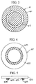
- FIGS. 4 and 5 show the phase plate employed in the projection exposure
apparatus shown in FIG. 1; FIG. 4 is a front view, while FIG. 5 is a cross-sectional view.
- FIG. 6 is a front view showing an index plate which is employed in the projection
exposure apparatus shown in FIG. 1.
- FIGS. 7 and 8 show alignment marks provided on a substrate; FIG. 7 is a front
view, while FIG. 8 is a cross-sectional view.
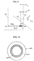
- FIG. 9 is an explanatory diagram showing the state in which baseline correction
is measured.
- FIG. 10 is a front view of an imaging light limiting member which is an example
of a member which modifies the optical characteristics which may be employed in the
projection exposure apparatus in place of the phase plate shown in FIG. 4.
- FIG. 11 is an explanatory diagram showing a conventional projection exposure
apparatus.
-
BEST MODE FOR CARRYING OUT THE INVENTION
-
Hereinbelow, an embodiment of the present invention will be explained in detail
with reference to FIGS. 1 to 10. With respect to the references in the figures which are
referred to in the explanation given hereinbelow, those which indicate the same objects as
in the explanation of the background art (FIG. 11) are given identical references.
Furthermore, the present invention is not necessarily limited to these embodiments; it is of
course that the structural elements of these embodiments may be appropriately combined.
-
FIG. 1 shows a projection exposure apparatus 1 in the present embodiment, while
FIG. 2 shows in expanded format a positional detection optical system (mark detection
system) Q of an off-axis type in FIG. 1. This positional detection optical system Q
generally comprises, as described above, an illumination optical part Q1, an imaging
optical part Q2, and an image processing part Q3. Hereinbelow, the structure of each of
these parts will be explained.
-
Illumination optical part Q1 is provided with an illumination light source Q1a, a
condenser lens Q1b, a wavelength selection element Q1c, an illumination field stop Q1d,
and a relay lens Q1e. Among these, a light source which generates broadband
illumination light (broadband light) such as a halogen lamp or the like is employed as
illumination light source Q1a. Furthermore, wavelength selection element Q1c only
permits the passage of wavelength bands of light to which the photoresist (photosensitive
agent) applied to the substrate W is insensitive. The 550 to 750 nm range, for example,
may be selected as the insensitive wavelength band of the photoresist. However, if the
present invention is applied to the positional detection of a substrate W which is not
covered with a photoresist, the restriction of the wavelength band described above is not
necessary. Furthermore, if an alignment mark A is formed for each layer, the wavelength
may be in the sensitive wavelength band, the wavelength breadth thereof may also be
freely selected, and either monochromatic light or semi-monochromatic light may be
employed. In the figure, an optical axis Q1X which extends from the illumination light
source Q1a to the substrate W is depicted. Furthermore, the illumination field stop Q1d
is a variable stop in which it is possible to modify at least one of the shape and size of the
opening thereof, and within illumination optical part Q1, the alignment mark A on
substrate W is provided in a plane which is essentially conjugate with the focal plane of an
objective lens Q1g which is discussed hereinbelow. Accordingly, the image of the
opening of the illumination field stop Q1d is projected onto the substrate W by a system
combining a relay lens Q1e and the objective lens Q1g. In other words, the detection
region of alignment mark A by positional detection optical system Q is determined by the
opening of the illumination field stop Q1d.
-
In illumination optical part Q1, in addition to the structure described above, an
illumination light limiting member (partial shielding plate) q1 is provided in a plane
(hereinbelow referred to as the illumination system pupil plane) which is in the
relationship of an optical Fourier transform with respect to the surface of the substrate W.
This is provided so that, by means of its function in concert with the phase plate q2, the
detection conditions of the alignment mark A on substrate W and the reference mark FM
on stage S are modified and thus the accuracy of the image recognition of the marks is
increased. Both members q1 and q2 described above correspond in the present
embodiment to the first modification device which modifies the optical conditions. The
first modification device is not necessarily limited to the members q1 and q2 described
above; members which modify the intensity distribution (at least one of the shape or size)
in the illumination system pupil plane of the illumination light irradiated onto alignment
mark A, or members which modify the imaging characteristics of the light emitted from
alignment mark A as a result of the irradiation of the illumination light, may be employed.
Furthermore, the first modification device may comprise only one or the other of members
q1 and q2.
-
As shown in FIG. 3, illumination light limiting member q1 has an annular
opening q12 formed in the flat surface comprising the darkening member q11.
Accordingly, the purpose of the actual function of the illumination light limiting member
q1 is to limit the passage of light emitted from the illumination light source Q1a and to
illuminate in an annular fashion the alignment mark A and the like on the substrate W.
However, this illumination light limiting member q1 is supported by a moveable member
q13, and depending on the surface state on the surface of the substrate W, this may be
inserted into or withdrawn from the optical axis Q1X. Accordingly, in the state in which
the illumination light limiting member q1 is withdrawn from the optical axis Q1X, normal
illumination is conducted with respect to the substrate W. That is to say, the illumination
light limiting member q1 has the function of modifying the intensity distribution in the
illumination system pupil plane of the illumination light irradiated onto the alignment
mark A1. For example, a plurality of illumination light limiting members in which at
least one of the shape and size of the opening differ may be provided on moveable
member q13, and one illumination light limiting member selected in accordance with the
type of substrate or resist or the formation conditions of the alignment mark (the including
the shape, step, or the like) may be disposed in the optical path of the illumination light
part Q1.
-
In illumination light part Q1, a beam splitter Q1f and an objective lens Q1g are
provided along the direction of travel of the light at a position beyond the illumination
light limiting member q1. By means of this, the light beam emitted from the
illumination light source Q1a is irradiated onto substrate W. The beam splitter Q1f and
the objective lens Q1g are provided on optical axis QX of imaging optical part Q2.
-
Next, the imaging optical part Q2 will be explained. In the order in which the
light reflected from the surface of the substrate W proceeds, the structure thereof is such
that, first, the objective lens Q1g and the beam splitter Q1f are disposed, and beyond these,
a phase plate q2, a relay lens Q2a, a beam splitter Q2b, an index plate Qk, a relay lens Q2c,
an illumination light limiting stop Q2d, a relay lens Q2e, and an image pickup element Qc
are disposed.
-
As described above, phase plate q2 has the function, in concert with the
illumination light limiting member q1, of increasing the accuracy of detection of the
alignment marks, particularly of low steps. This phase plate q2 is provided in a plane
(hereinbelow referred to as the imaging system pupil plane) which is in an optical Fourier
transform relationship with the substrate W. Accordingly, the phase plate q2 and the
illumination light limiting member q1 are mutually conjugate (imaging relationship).
Furthermore, this phase plate q2 is supported by a moveable member q21, and in the same
manner as the illumination light limiting member q1, this may be inserted into and
withdrawn from the optical axis QX.
-
As shown in FIGS. 4 and 5, phase plate q2 has an annular-shaped part q25 having
a multilayered structure in which a metal thin film q23 and a dielectric film q24 are
laminated, formed in a flat surface comprising a transparent body (a glass plate such as
silica or the like) q22. This annular-shaped part q25 is formed at a position which is
conjugate with the annular opening q12 of the illumination light limiting member q1.
Accordingly, the phase plate q2 has the function of conducting phase shifting with respect
to the zero order diffracted light emitted from the substrate W by the operation of this
annular-shaped part q25. Concretely, the amount of light transmitted is limited by the
metal thin film q23, and the phase of the transmitted light is shifted by the dielectric film
q24. By means of this, the light from the substrate W is such that a phase difference is
produced between the light passing through the annular-shaped part q25 in the phase plate
q2 and the light passing through other regions. This type of structure is the same as a
phase difference filter in a conventionally known phase contrast microscope, and by
providing this in the illumination optical system Q2, it is possible to increase the accuracy
of detection by modifying the imaging conditions of the alignment mark A. The film
thickness of the dielectric film q24 may be appropriately determined in accordance with
the index of diffraction n and the wavelength λ of the light source. A thickness t = λ
/(4(n-1)) obtaining a phase difference of π/2 (rad) may be used as an example. It is not
absolutely necessary to provide the metal thin film q23 which serves to limit the amount
of light transmitted.
-
As shown in FIG. 6, index plate Qk is a glass body (flat plate) which is provided
with index marks Qk1 which are darkening parts, and as explained in the "Background
Art" section, this serves as a reference when detecting the position of the image of the
index mark Qk1 on the index plate Qk and the position of the image formed by light
emitted from the alignment mark A on substrate W and transmitted by the phase plate q2.
The setting is such that the light from alignment mark A passes through the rectangular
region MI in FIG. 6. Furthermore, index plate Qk is disposed in a plane which is
essentially conjugate with the focal plane of the objective lens Q1g described above within
the imaging optical part Q2.
-
Furthermore, an index plate illumination system Qk2 which serves the purpose of
dedicated illumination is provided at the index plate Qk. This index plate illumination
system Qk2 comprises a light source Qk21, a condenser lens Qk22, an index plate
illumination field stop Qk23, and a relay lens Qk24. The light emitted from light source
Qk21 passes through the structural elements described above and is set so as to illuminate
only the pair of index marks Qk1 on index plate Qk via the beam splitter Q2b which is
provided in the optical axis QX. The index plate illumination system Qk2 described
above is not absolutely necessary. In the case where this system is not provided, for
example, light which directly enters from the substrate W (reflected light) may be
employed as the light which illuminates the index plate Qk in an unchanged manner.
-
Returning to FIG. 2, the imaging light limiting stop Q2d is disposed in a plane
having a conjugate relationship with the phase plate q2 described above. By means of
this, it is possible to freely modify the numerical aperture (N.A.) of the imaging optical
part Q.
-
The image pickup element Qc receives reflected light from substrate W which
passes through the imaging optical part Q described above and receives light from the
index marks Qk1 of the index plate Qk, recognizes this as an image (images) and converts
this to a digital signal. A CCD camera, an area image sensor, or the like, is commonly
employed for this.
-
Next, the image processing part Q3 will be described. This image processing
part Q3 processes the electrical signals emitted by the image pickup element Qc, and
outputs control signals which move the stage S in order to realize alignment. This image
processing part Q3 comprises an amplifier Q31, an A/D converter Q32, an alignment
controller (controlling unit) Q33, and a baseline memory (storage unit) Q34. Among
these, the alignment controller Q33 and the baseline memory Q34 function as a baseline
correcting device which conducts the actual correction of the baseline.
-
Amplifier Q31 is provided in order to amplify, by a desired amplification ratio,
the electrical signal based on the image recognized in the image pickup element Qc, that is
to say, the alignment mark detection signal. The amplification ratio at this time is
fundamentally freely selected; depending on the state of the strength of the electrical
signal of the incorporated image (the amplitude, the signal to noise ratio and the like) it is
possible to carry out modification of the amplification factor in an appropriate fashion.
In other words, in the present embodiment, this amplifier Q31 corresponds to the second
modification device which modifies the electrical circuit characteristics, and moreover,
conducts the modification of the detection conditions of the positional detection optical
system Q.
-
The A/D converter Q32 is provided in order to convert the electrical signal
amplified above from an analog signal to a digital signal. The alignment controller Q33
is provided in order to arithmetically process the digital signal outputted from the A/D
converter Q32. Concretely, the positions of the image resulting from the reflected light
from the alignment mark A on substrate W and the image of the index marks Qk1 of the
index plate Qk are compared to one another, and inputting the position of the stage S as
detected by a laser interferometer LC described hereinbelow, the position of the alignment
mark A on substrate W is detected. Furthermore, the alignment controller Q33 conducts
alignment based on the position detected. Additionally, the alignment controller Q33
conducts data exchange among the illumination light limiting member q1, phase plate q2,
and amplifier Q31 described above. Concretely, the controller transmits, to the
illumination light limiting member q1 and to the phase plate q2, data relating to the
insertion or withdrawal state from the optical axis, and transmits, to amplifier Q31, data
relating to the amplification factor. In addition to this, the alignment controller Q33 is
connected with a baseline memory Q34 which is described hereinbelow, and conducts the
writing and readout of data in this memory Q34.
-
Baseline memory Q34 is a memory which serves to store baseline correction
values generated as a result of the modification of the optical characteristics or the
electrical circuit characteristics of the positional detection optical system Q. Furthermore,
this baseline memory Q34 is a region which stores baseline amounts measured by the
positional detection optical system Q when modifications are not undergone by the optical
characteristics modification device or the electrical circuit characteristics modification
device.
-
Above, the details of the structure of the position optical detection mechanism Q
were discussed; however, in addition, a projection optical system P and a stage S and the
like are provided in the present embodiment. These are the same as those which where
explained in the "Background Art" section above. As is shown in FIG. 1, a reticle R is
disposed on the object surface side of projection optical system P, and the pattern surface
thereof is transferred by exposure illumination light (exposure beam) by means of an
illumination optical system which is not depicted in the figure. The illumination optical
system employs, as the exposure illumination light, beams generated by a mercury lamp
(for example, g line, i line), or higher harmonics or the like of KrF excimer lasers
(wavelength 248 nm), ArF excimer lasers (wavelength 193 nm), F2 lasers (wavelength 157
nm), or YAG lasers or metal vapor lasers. In projection optical system P, a plurality of
refraction optical elements are lined up along the optical axis, and these reduce the image
of the pattern of reticle R and project it onto substrate W. The projection optical system
P may be a reflection-refraction optical system, in which a plurality of reflection optical
elements, including mirrors or concave mirrors having a reflecting surface which is
non-spherical, are combined with a plurality of refraction optical elements. In the
present embodiment, the projection optical system P has a circular field of view and is a
double-sided telecentric reducing system. Reticle R is supported by a reticle stage (not
depicted in the figure) which is disposed at the object side thereof so that the pattern
surface thereof is disposed in a first plane (object plane) which is perpendicular to the
optical axis PX of the projection optical system P.
-
An alignment optical system RA is disposed above reticle R; this receives the
light which is emitted from the reference mark FM on index plate PT which disposed at
stage S as a result of the illumination of the exposure illumination light and which passes
through the projection optical system P, as well as the light which is emitted from the
reticle marks Rm, in an image pickup element (CCD) via an objective optical system, and
detects the amount of positional displacement of the images of the two marks. This
alignment optical system RA is employed during the baseline measurement described
hereinbelow, and the measurement operation is the same as that explained in the case of
FIG. 11.
-
A stage S, which supports substrate W and which is capable of two-dimensional
movement within a plane perpendicular to the optical axis PX of the projection optical
system P, is disposed at the image surface side of projection optical system P, and the
position thereof is constantly measured by a laser interferometer LC. The substrate W is
supported by the stage S within the view field of projection optical system P, that is to say,
within the illumination region of the exposure illumination light, so that the exposure
plane (for example, the surface) of the substrate W is disposed within a second plane
(image plane) which is perpendicular to the optical axis PX. A reference plate PT is
provided on stage S, and a reference mark FM which is employed during baseline
measurement is formed on the reference plate PT. The reference mark FM contains two
groups of line and space patterns having periodicities in the X and Y directions. The
output signal of the laser interferometer LC is inputted into the alignment controller Q33
and into the main control apparatus Z which conducts all control of the entirety of the
exposure apparatus. The alignment controller Q33 detects the position (coordinate
values) of the alignment mark A on substrate W and the reference mark FM as described
above, and the main control apparatus Z controls the drive of the stage S via a stage drive
system which is not depicted in the figure, based on the position determined and the
output of laser interferometer LC, and executes the alignment and the like of the shot
region on the substrate W and the pattern image of the reticle R.
-
A mark comprising three band-shaped concavities disposed with a period of E, an
example of which is shown in FIGS. 7 and 8, may be used as the alignment mark A which
is provided on substrate W. As described above, this alignment mark A is provided in
order to conduct a comparison of the relative positions with the index mark Qk1 in
positional displacement optical system Q, and to calculate the correct position of stage S.
In other words, by considering the relative distance between the image of index mark Qk1
and the image of alignment mark A in image pickup element Qk, it is possible to conduct
alignment.
-
The functional results of a projection exposure apparatus 1 having the structure
described above will now be explained. The essential feature of the present embodiment
is the measurement of the baseline amount, so that an explanation of the details of the
remainder of the exposure operation will be omitted. When the alignment mark A on
substrate W is detected by positional detection optical system Q and a predetermined
correction amount (offset) is added to the positional information (coordinate values)
outputted by the alignment controller Q33, and stage S is moved, the image of reticle mark
Rm projected by projection optical system P is essentially in agreement with the alignment
mark A. This correction amount is the baseline amount referred to above.
-
First, in positional detection optical system Q, when illumination light limiting
member q1 and phase plate q2 are not disposed on optical axes Q1X and QX, and when
the amplifier Q31 has a fixed amplification factor, as shown in FIG. 9, the baseline
amount is calculated, and this is designated Borg. In other words, this baseline amount
Borg is the baseline amount of the initial state of the optical characteristics and electrical
circuit characteristics in the positional detection optical system Q. This baseline amount
Borg is stored in baseline memory Q34.
-
Next, the baseline amount is measured in a case in which the illumination light
limiting member q1 and the phase plate q2 are disposed in the respective optical axes Q1X
and QX, and this is designated Bopt. The baseline memory Q34 stores this Bopt. As
shown for example in FIG. 9, this baseline amount Bopt is in a state in which there is a
difference of only Δ B (not equal to 0) from the baseline amount Borg described above.
That is to say, Δ B corresponds to the correction value (detection error) of the baseline
amount with respect to Borg. In FIG. 9, by inserting the illumination light limiting
member q1 and the phase plate q2, the optical axis QX is apparently shifted to the optical
axis QX', and even if the image of the alignment mark A is correctly detected in image
pickup element Qc, the appropriate baseline amount is not Borg, but Bopt.
-
With respect to the disposition of the illumination light limiting member q1 in the
optical path Q1X, in addition to the shift of the optical axis described above, the problem
of aberration must also be considered. It is impossible to completely avoid the
occurrence of such aberration; however, it is thought that the presence or absence of the
illumination light limiting member q1 in the optical axis Q1X has an effect on the degree
of such aberration. In other words, the disposition of the illumination light limiting
member q1 in the optical axis Q1X, when compared with the case in which this member is
not inserted into the optical path, changes the state of the light beam of the illumination
optical system Q1 and this changes the illumination conditions of the alignment mark A,
so that by means of this, the degree of aberration is thought to be larger (or smaller) in one
or the other case. This has an effect on the image in the image pickup element Qc which
comparable to the shift in optical axis QX described above. Accordingly, it is necessary
to assume that the baseline amount Bopt described above incorporates the effects of the
disparity of this aberration.
-
Furthermore, the amplifier Q31 is set in advance to a freely selected amplification
factor which is arithmetically selected (modification of the electrical circuit
characteristics) and in accordance with this, changes Bele1, Bele2 ... in the baseline
amount are measured and these are stored in advance in the baseline memory Q34.
When the amplification factor of this amplifier Q31 is changed, modulation is applied to
the electrical signal from the image pickup element Qc. For example, as the
amplification factor increases, this tends to lead to a time delay and an increase in the
necessary elements. As a result, in the alignment controller Q33, an image containing
displacements such as horizontal or vertical shifts or the like, which differs from the signal
distribution of the image actually observed in the image pickup element Qc, is observed.
The changes Bele1, Bele2, ... in the baseline amount described above correspond precisely
thereto. If the difference from the Borg described above is obtained with respect to these
baseline amounts Bele1, Bele2, ..., as well, then in general, displacement amounts Δ B1,
Δ B2, ..., which are not 0 are present. These Δ B1, Δ B2, ... correspond to correction
values (detection errors) of the baseline amounts, in the same way as the Δ B described
above. In this way, by storing correction values of the baseline amounts with respect to
amplification factors, it is possible to know the appropriate baseline amount for each
amplification factor.
-
When the alignment of substrate W is actually executed as described above, this
is conducted in a state in which the various baseline values Borg, Bopt, Bele1, Bele2, ...
are stored in the baseline memory Q34. For example, if an alignment mark A provided
on a conveyed substrate W is clearly discernible in a standard positional detection optical
system Q (image processing part Q3), then alignment controller Q33 conducts alignment
without inserting the illumination light limiting member q1 or the phase plate q2 into the
optical axis by selecting baseline amount Borg from baseline memory Q34.
-
On the other hand, in the case where the alignment mark A is, for example, a low
step mark as a result of a flattening process and the image in the image pickup element Qc
is unclear (inappropriate for positioning), then attempts are made to insert the illumination
light limiting member q1 and the phase plate q2 into the optical axis and modify the
optical characteristics, or to adjust the amplification factor of amplifier Q31 and thus
modify the electrical circuit characteristics or the like, If at this time the image of the
alignment mark A becomes clear as result of, for example, modification of the optical
characteristics, then data incorporating this modification of the optical characteristics are
sent from the illumination light limiting member q1 and the phase difference q2 to the
alignment controller q33, and based on these data, the alignment controller q33 selects the
baseline amount Bopt from the baseline memory Q34 and conducts the alignment of
substrate W. This processing method is applied in exactly the same manner in the case of
a modification of the electrical circuit characteristics.
-
In this way, in accordance with the projection exposure apparatus of the present
embodiment, with respect to changes in the optical characteristics and electrical circuit
characteristics in the positional detection optical system Q, the baseline amounts Borg,
Bopt, Bele1, Bele2, ... are measured in advance, and these are stored in advance in the
baseline memory Q34, and thereby, alignment controller Q33 selects the appropriate
baseline amount from among the baseline amounts Borg, Bopt, Bele1, Bele2, and the like
based on the changes in the characteristics, and conducts alignment, so that appropriate
exposure is always executed. This means that the manufacture of products having stable
quality is possible without suffering the effects of changes in the optical characteristics
(reflectivity, diffraction and the like) or shape of the alignment mark A provided on the
substrate W. In the embodiment described above, each time optical characteristics and
electrical circuit characteristics were combined, the corresponding baseline amount or the
correction value thereof was stored; however, a function expressing the relationship
between the combination of optical characteristics and electrical circuit characteristics and
the corresponding amount of fluctuation in the baseline amount may be stored in advance
in the memory, and the baseline amount or the amount of fluctuation thereof (in other
words, the correction value) may be calculated based on the selected combination of
characteristics and the function which is stored for this combination when the alignment
mark is detected.
-
As described in the embodiment above, the present invention is not limited to a
form in which alignment is conducted by storing baseline amounts Borg, Bopt, Bele1,
Bele2, ... corresponding to the various changes in characteristics, in baseline memory Q34.
For example, the following type of alignment may be conducted. As shown in FIG. 1,
the modification of the optical characteristics described above, that to say, the insertion of
illumination light limiting member q1 and phase plate q2 into the optical axes, is
conducted by movable members q13 and q21. Accordingly, when the members q1 and
q2 are inserted into the optical axes, it can be inferred that there will be some physical
displacement resulting from errors in attachment to the moveable members q13 and q21 or
from errors in movement thereof during insertion. This physical displacement is
generally impossible to predict in advance, so that in cases of processing of products
which require particular accuracy, it is preferable that instead of selecting Bopt during the
modification of the optical characteristics, exposure be conducted while measuring the
baseline amount for each modification of the characteristics. In other words, in the
detection of the alignment mark A in semiconductor W, in cases corresponding to
modifications of the optical characteristics of the positional detection optical system Q
when the image is unclear, exposure is conducted after measuring the baseline amount
each time.
-
The circumstances described above are the same in modifications of the electrical
circuit characteristics in the positional detection optical system Q, that is to say, in the case
of the modification of the amplification factor of the amplifier Q31, and thereby, in these
cases as well, it is possible to measure the baseline amount for each modification of the
characteristics and to conduct exposure operations.
-
If alignment is conducted by measuring the baseline amount for each set of
characteristics in this manner, then in comparison with operations in which the baseline
memory Q34 is employed as described above, alignment may be conducted more reliably
and with higher accuracy. However, in these cases, the throughput naturally falls, so that
the choice of which method to employ in conducting exposure is determined in view of
the conditions and the accuracy and the like required in the products.
-
Furthermore, when the baseline is measured in the embodiment described above,
the reference mark FM formed on the reference plate PT on stage S is detected in the
manner of a time series with, respectively, the alignment optical system RA and the
positional detection optical system Q. However, as disclosed, for example, in Japanese
Patent Application, First Publication No. HEI 4-324923 and the corresponding United
States Patent No. 5,243,195, first and second reference marks PT are formed separated by
an interval corresponding to the baseline amount of the positional detection optical system
Q of the off-axis type, and simultaneously with the detection of the first reference mark by
the alignment optical system RA, the second reference mark is detected by the positional
detection optical system Q. Then, the baseline amount may be determined based on the
detection results of the two optical systems, the measured result of the interferometer LC,
and the interval between the first and second reference marks. By means of this, it is
possible to conduct baseline measurement without removing the stage S, so that it is
possible to shorten the measurement time, and to increase the accuracy of measurement.
This disclosure and the disclosure of the United States patent are incorporated in the
disclosure of the present document insofar as this is permitted by the domestic law of the
countries designated in the present international application or countries which are
selected.
-
With respect to the embodiment explained above, supplementary items are
discussed hereinbelow.
-
First, an illumination light limiting member q1 and a phase plate q2 were
provided in the above embodiment as the modification device for the optical
characteristics in the positional detection optical system Q; however, the present invention
is not particularly limited to this structure. For example, in place of the phase plate q2, it
is possible to employ an illumination light limiting member q20 such as that shown in FIG.
10. Herein, an annular-shaped darkening part Q202 is formed in the flat plate comprising
a transparent body q201. As is clear from this figure, the imaging light limiting member
q20 is not outwardly greatly different from the phase plate q2. However, the darkening
part q202 is formed at a position which does not allow the passage of the zero-order
diffracted light among the light emitted from the substrate W. In other words, in the
same way as in the fundamental principle of the so-called dark field microscope, only the
first order or higher diffracted light is transmitted. By means of this type of imaging
light limiting member q20, it is possible to obtain clear images even in cases in which the
step of the alignment mark A is particularly small. Even in the case in which this
imaging light limiting member q20 is inserted into the optical path QX, the light beams
pass through the transparent body q201, so that it is quite possible that this will cause
dislocation or the like of the optical axis QX. Accordingly, even in the case of a
positional detection optical system Q which is provided with this type of imaging light
limiting member q20, by applying a projection exposure apparatus 1 in accordance with
the present invention, it is possible to obtain suitable results.
-
The modification of the optical characteristics is not necessarily limited to the
form described above; even in the case in which the illumination light source Q1a of the
illumination optical system Q1 in the positional detection optical system Q, that is to say,
the intensity distribution of the illumination light (the shape or size of the secondary light
source) in the pupil plane of the illumination optical part Q1, is modified, it is of course
possible to modify the optical characteristics. In this case, as well, it is clear that if
baseline correction is conducted in accordance with the present embodiment, reliable
exposure may be conducted.
-
In the present embodiment, the modification of the electrical circuit
characteristics in the positional detection optical system Q was conducted by an increase
or decrease in the amplification ratio of the amplifier Q31; however, the modification of
the electrical circuit characteristics is not limited to this method. For example, in the
image processing part Q3 shown in FIG. 1, a noise filter or the like may be added into the
circuitry in order to increase the reliability of the detection signal; however, this may also
be used to modify the electrical circuit characteristics. In this case, when this noise filter
is inserted into the circuitry, and when the noise filter is not present in the circuitry, the
measurement of the baseline amount and the correction values may be stored in advance in
the baseline memory Q34.
-
Additionally, with respect to calculations in which the alignment controller Q33
and the baseline memory Q34 are concerned, in the case of the embodiment described
above, the baseline amounts Borg, Bopt, Bele1, Bele2, . . . are directly stored, and the
alignment controller Q33 selects each baseline amount for each modification of the
characteristics. However, the calculation processing is not necessarily limited to this
form, and for example, the differences between Borg and the other baseline amounts Bopt,
Bele1, Bele2, . . . may be stored in baseline memory Q34 as Δ B, Δ B1, Δ B2, . . ., and a
processing method may be adopted in which the accurate baseline amounts are obtained
by adding or subtracting these to or from Borg.
-
Furthermore, in the embodiment described above, in addition to the projection
optical system P, a separate offset-type positional detection optical system Q, in which a
objective optical system was disposed, was employed; however, a positional detection
optical system of the TTL (Through The Lens) type, in which illumination light is
irradiated onto the alignment mark on substrate W via the projection optical system P and
the light which is emitted from the mark and passes through the projection optical system
P is received, or a positional detection optical system of the TTR (through the reticle) type,
in which the alignment mark on the substrate and the alignment mark on the reticle are
detected via the projection optical system P, may be employed.
-
Furthermore, even in the case in which a positional detection optical system
which conducts the image pickup of the alignment mark is not employed, but rather a
positional detection optical system is employed in which, for example, two coherent
beams are irradiated onto the alignment mark on the substrate, and the diffracted light
emitted in essentially the same direction from the mark is received, or in the case in which
a positional detection optical system is employed in which the plus or minus one order
diffracted light which is generated from the alignment mark by the irradiation of the
coherent beams and which passes through the projection optical system P is irradiated
onto the reticle mark, and two diffracted light beams emitted from the reticle marks are
received, it is desirable to calculate the baseline amount or the correction values for each
set of characteristics, in the same way as in the present embodiment, when the optical
characteristics or the electrical characteristics of the positional detection optical system are
modified in accordance with a modification of the formation conditions of the alignment
mark (the pitch or the like). That is to say, the present invention may be applied with
respect to the positional detection optical system irrespective of the type of detection of
the alignment mark, and is capable of obtaining the same effects in all cases.
-
Furthermore, the positional detection optical system described above is capable of
application not merely to reduction projection type exposure apparatuses of the step and
repeat type (steppers) or reduction projection type scanning exposure apparatuses of the
step and scan type (scanning steppers) but also to all exposure apparatuses, including
proximity types and mirror projection types. Furthermore, the positional detection
optical system of FIG. 1 may be applied with respect to exposure apparatuses which
employ hard X-rays or charged particle beams (electron beams or ion beams or the like),
or to exposure apparatuses which employ light having oscillation spectra within a range of
5 to 15 nm (the soft X-ray band), such as, for example, EUV (extreme ultraviolet) light
having a wavelength of 13.4 nm or 11.5 nm. Projection exposure apparatuses which
employ EUV light are provided with a reduction projection optical system which
prescribes the illumination regions on a reflection mask using arc slits and which
comprises a plurality of reflection optical elements (mirrors), and the reflection mask and
the substrate are moved simultaneously at a velocity ratio which is in accordance with the
magnification factor of the reducing projection optical system, and thus the pattern on the
reflection on the reflection mask is transferred onto the substrate.
-
In the embodiment described above, the baseline amount was corrected in
accordance with the modification of the detection conditions (optical characteristics,
electrical circuit characteristics and the like) of the alignment mark by means of the
positional detection optical system; however, the detection error of the alignment mark
produced as a result of the modification of the detection conditions may be added as an
offset to the positional information (the coordinate values on an orthogonal coordinate
system XY defined by an interferometer LC, or the amount of positional displacement
from the reference mark Qk1) of the alignment mark detected by the positional detection
optical system Q. Alternatively, so that the amount of fluctuation in the baseline amount
(the detection error in the alignment mark) produced by the modification of the detection
conditions is canceled out, the exposure position of the reticle R may be modified in
accordance with this amount of fluctuation (detection error). In other words, in the static
exposure method, the stoppage position of the reticle R may be shifted, while in the
scanning exposure method, the scanning exposure (or acceleration) initiation position of
the reticle R may be shifted. In short, the exposure position of substrate W with respect
to reticle R should be corrected in accordance with the modification of the detection
conditions, and any of the baseline amount of the positional detection optical system Q,
the positional information of the alignment mark detected by the positional detection
optical system Q, or the exposure position of reticle R, may be corrected. Furthermore,
the exposure position of the substrate W is determined by the baseline amount and the
positional information of the alignment mark, so that in the present invention, at least one
of the exposure position of the substrate W and the exposure position of the reticle R, that
is to say, the relative exposure position data of the substrate W and the reticle R, is
corrected in accordance with the modification of the detection conditions of the positional
detection optical system Q.
-
Furthermore, the projection optical system PL is not limited to a refraction system
comprising a plurality of refraction optical elements; a reflection-refraction system having
refraction optical elements and reflection optical elements (concave mirrors or the like), or
a reflection system comprising solely a plurality of reflection optical elements, may be
employed. Here, as the reflection-refraction type projection optical system, there are
optical systems which are provided with at least a beam splitter and concave minor
reflection optical elements, optical systems which are provided with no beam splitters, but
are provided with concave minors and minors as reflection optical elements, and optical
systems which, as disclosed in United States Patent No. 5,788,229, have two reflection
optical elements (at least one of which is a concave mirror) and a plurality of refraction
optical elements disposed along a single optical axis. The disclosure of this United
States patent is incorporated by reference into the disclosure of the present document
insofar as this is permitted by the domestic law of the countries designated in the present
international application, as well as selected countries. Furthermore, the projection
optical system P may be an enlarging type, a reducing type, or a non-magnifying type.
Furthermore, the present invention may be applied even if a projection optical system is
not employed, such as, for example, in proximity type exposure apparatuses.
-
Furthermore, in place of an extra-high pressure mercury lamp, an excimer laser,
or an F2 laser or the like, it is also possible to employ higher harmonics in which a
single-wavelength laser in the infrared band or the visible band is oscillated from an DFB
semiconductor laser or a fiber laser and is amplified by a fiber amplifier doped with
erbium (or with both erbium and ytterbium), and this is frequency-converted to ultraviolet
light using non-linear optical crystals. As an example of this, if the oscillation
wavelength of the single-wavelength laser is set to a range of 1.51 to 1.59 micrometers,
then the eightfold higher harmonic, the generation wavelength of which is within a range
of 189 to 199 nm, or the tenfold higher harmonic, the generation wavelength of which is
within a range of 151 to 159 nm, is outputted. In particular, if the oscillation wavelength
is set within a range of 1.544 to 1.553 micrometers, then the eightfold higher harmonic,
within a range of 193 to 194 nm, that is to say, ultraviolet light having a wavelength which
is essentially the same as that of a ArF excimer laser, is obtained, and if the oscillation
wavelength is within a range of 1.57 to 1.58 micrometers, then the tenfold higher
harmonic within a range of 157 to 158 nm, that is to say, ultraviolet light having a
wavelength which is essentially the same as that of a F2 laser, is obtained.
-
The present invention is not limited to the production of microprocessors such as
semiconductor elements and the like; it may be applied in exposure apparatuses which
transfer a circuit pattern onto a glass substrate or a silicon wafer or the like in order to
produce reticles or masks used in, for example, light exposure apparatuses, EUV exposure