EP1020947A2 - Method for manufacturing an antenna body for a phone and phone or handset having an internal antenna - Google Patents
Method for manufacturing an antenna body for a phone and phone or handset having an internal antenna Download PDFInfo
- Publication number
- EP1020947A2 EP1020947A2 EP99310154A EP99310154A EP1020947A2 EP 1020947 A2 EP1020947 A2 EP 1020947A2 EP 99310154 A EP99310154 A EP 99310154A EP 99310154 A EP99310154 A EP 99310154A EP 1020947 A2 EP1020947 A2 EP 1020947A2
- Authority
- EP
- European Patent Office
- Prior art keywords
- antenna
- dielectric body
- resin
- phone
- dielectric
- Prior art date
- Legal status (The legal status is an assumption and is not a legal conclusion. Google has not performed a legal analysis and makes no representation as to the accuracy of the status listed.)
- Pending
Links
- 238000000034 method Methods 0.000 title claims description 21
- 238000004519 manufacturing process Methods 0.000 title claims description 12
- 239000011347 resin Substances 0.000 claims abstract description 36
- 229920005989 resin Polymers 0.000 claims abstract description 36
- 239000002184 metal Substances 0.000 claims abstract description 30
- 229910052751 metal Inorganic materials 0.000 claims abstract description 30
- 238000001746 injection moulding Methods 0.000 claims abstract description 21
- 238000000576 coating method Methods 0.000 claims abstract description 13
- 239000002131 composite material Substances 0.000 claims abstract description 9
- 239000011248 coating agent Substances 0.000 claims abstract description 6
- 230000001070 adhesive effect Effects 0.000 claims abstract description 3
- 230000008878 coupling Effects 0.000 claims description 14
- 238000010168 coupling process Methods 0.000 claims description 14
- 238000005859 coupling reaction Methods 0.000 claims description 14
- 239000000463 material Substances 0.000 claims description 11
- 150000001875 compounds Chemical class 0.000 claims description 4
- PPBRXRYQALVLMV-UHFFFAOYSA-N Styrene Chemical group C=CC1=CC=CC=C1 PPBRXRYQALVLMV-UHFFFAOYSA-N 0.000 claims description 3
- 239000003054 catalyst Substances 0.000 claims description 3
- 229920000642 polymer Polymers 0.000 claims description 3
- 230000001846 repelling effect Effects 0.000 claims description 3
- 239000004033 plastic Substances 0.000 description 8
- IUYHQGMDSZOPDZ-UHFFFAOYSA-N 2,3,4-trichlorobiphenyl Chemical compound ClC1=C(Cl)C(Cl)=CC=C1C1=CC=CC=C1 IUYHQGMDSZOPDZ-UHFFFAOYSA-N 0.000 description 6
- 238000007747 plating Methods 0.000 description 6
- 239000003989 dielectric material Substances 0.000 description 5
- XLYOFNOQVPJJNP-UHFFFAOYSA-N water Substances O XLYOFNOQVPJJNP-UHFFFAOYSA-N 0.000 description 5
- 230000001427 coherent effect Effects 0.000 description 4
- 210000002105 tongue Anatomy 0.000 description 4
- 229920010524 Syndiotactic polystyrene Polymers 0.000 description 3
- 238000010521 absorption reaction Methods 0.000 description 3
- 238000004891 communication Methods 0.000 description 3
- 238000000465 moulding Methods 0.000 description 3
- 230000005855 radiation Effects 0.000 description 3
- PXHVJJICTQNCMI-UHFFFAOYSA-N Nickel Chemical compound [Ni] PXHVJJICTQNCMI-UHFFFAOYSA-N 0.000 description 2
- 230000001413 cellular effect Effects 0.000 description 2
- 230000003247 decreasing effect Effects 0.000 description 2
- 230000009977 dual effect Effects 0.000 description 2
- 238000001465 metallisation Methods 0.000 description 2
- 238000003801 milling Methods 0.000 description 2
- 239000000243 solution Substances 0.000 description 2
- 230000010267 cellular communication Effects 0.000 description 1
- ZCDOYSPFYFSLEW-UHFFFAOYSA-N chromate(2-) Chemical compound [O-][Cr]([O-])(=O)=O ZCDOYSPFYFSLEW-UHFFFAOYSA-N 0.000 description 1
- 238000006073 displacement reaction Methods 0.000 description 1
- 238000005553 drilling Methods 0.000 description 1
- 230000000694 effects Effects 0.000 description 1
- 230000005672 electromagnetic field Effects 0.000 description 1
- 239000007924 injection Substances 0.000 description 1
- 238000002347 injection Methods 0.000 description 1
- 239000007769 metal material Substances 0.000 description 1
- 229910052759 nickel Inorganic materials 0.000 description 1
- 230000002093 peripheral effect Effects 0.000 description 1
- DQMZLTXERSFNPB-UHFFFAOYSA-N primidone Chemical compound C=1C=CC=CC=1C1(CC)C(=O)NCNC1=O DQMZLTXERSFNPB-UHFFFAOYSA-N 0.000 description 1
- 239000012899 standard injection Substances 0.000 description 1
- 238000010998 test method Methods 0.000 description 1
- 210000005182 tip of the tongue Anatomy 0.000 description 1
Images


Classifications
-
- H—ELECTRICITY
- H01—ELECTRIC ELEMENTS
- H01Q—ANTENNAS, i.e. RADIO AERIALS
- H01Q13/00—Waveguide horns or mouths; Slot antennas; Leaky-waveguide antennas; Equivalent structures causing radiation along the transmission path of a guided wave
- H01Q13/10—Resonant slot antennas
-
- B—PERFORMING OPERATIONS; TRANSPORTING
- B29—WORKING OF PLASTICS; WORKING OF SUBSTANCES IN A PLASTIC STATE IN GENERAL
- B29C—SHAPING OR JOINING OF PLASTICS; SHAPING OF MATERIAL IN A PLASTIC STATE, NOT OTHERWISE PROVIDED FOR; AFTER-TREATMENT OF THE SHAPED PRODUCTS, e.g. REPAIRING
- B29C45/00—Injection moulding, i.e. forcing the required volume of moulding material through a nozzle into a closed mould; Apparatus therefor
- B29C45/0053—Injection moulding, i.e. forcing the required volume of moulding material through a nozzle into a closed mould; Apparatus therefor combined with a final operation, e.g. shaping
-
- B—PERFORMING OPERATIONS; TRANSPORTING
- B29—WORKING OF PLASTICS; WORKING OF SUBSTANCES IN A PLASTIC STATE IN GENERAL
- B29C—SHAPING OR JOINING OF PLASTICS; SHAPING OF MATERIAL IN A PLASTIC STATE, NOT OTHERWISE PROVIDED FOR; AFTER-TREATMENT OF THE SHAPED PRODUCTS, e.g. REPAIRING
- B29C45/00—Injection moulding, i.e. forcing the required volume of moulding material through a nozzle into a closed mould; Apparatus therefor
- B29C45/16—Making multilayered or multicoloured articles
-
- C—CHEMISTRY; METALLURGY
- C23—COATING METALLIC MATERIAL; COATING MATERIAL WITH METALLIC MATERIAL; CHEMICAL SURFACE TREATMENT; DIFFUSION TREATMENT OF METALLIC MATERIAL; COATING BY VACUUM EVAPORATION, BY SPUTTERING, BY ION IMPLANTATION OR BY CHEMICAL VAPOUR DEPOSITION, IN GENERAL; INHIBITING CORROSION OF METALLIC MATERIAL OR INCRUSTATION IN GENERAL
- C23C—COATING METALLIC MATERIAL; COATING MATERIAL WITH METALLIC MATERIAL; SURFACE TREATMENT OF METALLIC MATERIAL BY DIFFUSION INTO THE SURFACE, BY CHEMICAL CONVERSION OR SUBSTITUTION; COATING BY VACUUM EVAPORATION, BY SPUTTERING, BY ION IMPLANTATION OR BY CHEMICAL VAPOUR DEPOSITION, IN GENERAL
- C23C18/00—Chemical coating by decomposition of either liquid compounds or solutions of the coating forming compounds, without leaving reaction products of surface material in the coating; Contact plating
- C23C18/16—Chemical coating by decomposition of either liquid compounds or solutions of the coating forming compounds, without leaving reaction products of surface material in the coating; Contact plating by reduction or substitution, e.g. electroless plating
- C23C18/1601—Process or apparatus
- C23C18/1603—Process or apparatus coating on selected surface areas
- C23C18/1607—Process or apparatus coating on selected surface areas by direct patterning
- C23C18/161—Process or apparatus coating on selected surface areas by direct patterning from plating step, e.g. inkjet
-
- C—CHEMISTRY; METALLURGY
- C23—COATING METALLIC MATERIAL; COATING MATERIAL WITH METALLIC MATERIAL; CHEMICAL SURFACE TREATMENT; DIFFUSION TREATMENT OF METALLIC MATERIAL; COATING BY VACUUM EVAPORATION, BY SPUTTERING, BY ION IMPLANTATION OR BY CHEMICAL VAPOUR DEPOSITION, IN GENERAL; INHIBITING CORROSION OF METALLIC MATERIAL OR INCRUSTATION IN GENERAL
- C23C—COATING METALLIC MATERIAL; COATING MATERIAL WITH METALLIC MATERIAL; SURFACE TREATMENT OF METALLIC MATERIAL BY DIFFUSION INTO THE SURFACE, BY CHEMICAL CONVERSION OR SUBSTITUTION; COATING BY VACUUM EVAPORATION, BY SPUTTERING, BY ION IMPLANTATION OR BY CHEMICAL VAPOUR DEPOSITION, IN GENERAL
- C23C18/00—Chemical coating by decomposition of either liquid compounds or solutions of the coating forming compounds, without leaving reaction products of surface material in the coating; Contact plating
- C23C18/16—Chemical coating by decomposition of either liquid compounds or solutions of the coating forming compounds, without leaving reaction products of surface material in the coating; Contact plating by reduction or substitution, e.g. electroless plating
- C23C18/1601—Process or apparatus
- C23C18/1633—Process of electroless plating
- C23C18/1635—Composition of the substrate
- C23C18/1639—Substrates other than metallic, e.g. inorganic or organic or non-conductive
- C23C18/1641—Organic substrates, e.g. resin, plastic
-
- H—ELECTRICITY
- H01—ELECTRIC ELEMENTS
- H01Q—ANTENNAS, i.e. RADIO AERIALS
- H01Q1/00—Details of, or arrangements associated with, antennas
- H01Q1/12—Supports; Mounting means
- H01Q1/22—Supports; Mounting means by structural association with other equipment or articles
- H01Q1/24—Supports; Mounting means by structural association with other equipment or articles with receiving set
- H01Q1/241—Supports; Mounting means by structural association with other equipment or articles with receiving set used in mobile communications, e.g. GSM
- H01Q1/242—Supports; Mounting means by structural association with other equipment or articles with receiving set used in mobile communications, e.g. GSM specially adapted for hand-held use
- H01Q1/243—Supports; Mounting means by structural association with other equipment or articles with receiving set used in mobile communications, e.g. GSM specially adapted for hand-held use with built-in antennas
-
- H—ELECTRICITY
- H01—ELECTRIC ELEMENTS
- H01Q—ANTENNAS, i.e. RADIO AERIALS
- H01Q1/00—Details of, or arrangements associated with, antennas
- H01Q1/36—Structural form of radiating elements, e.g. cone, spiral, umbrella; Particular materials used therewith
- H01Q1/38—Structural form of radiating elements, e.g. cone, spiral, umbrella; Particular materials used therewith formed by a conductive layer on an insulating support
-
- H—ELECTRICITY
- H01—ELECTRIC ELEMENTS
- H01Q—ANTENNAS, i.e. RADIO AERIALS
- H01Q5/00—Arrangements for simultaneous operation of antennas on two or more different wavebands, e.g. dual-band or multi-band arrangements
- H01Q5/30—Arrangements for providing operation on different wavebands
- H01Q5/307—Individual or coupled radiating elements, each element being fed in an unspecified way
- H01Q5/342—Individual or coupled radiating elements, each element being fed in an unspecified way for different propagation modes
- H01Q5/357—Individual or coupled radiating elements, each element being fed in an unspecified way for different propagation modes using a single feed point
- H01Q5/364—Creating multiple current paths
- H01Q5/371—Branching current paths
-
- H—ELECTRICITY
- H01—ELECTRIC ELEMENTS
- H01Q—ANTENNAS, i.e. RADIO AERIALS
- H01Q9/00—Electrically-short antennas having dimensions not more than twice the operating wavelength and consisting of conductive active radiating elements
- H01Q9/04—Resonant antennas
- H01Q9/0407—Substantially flat resonant element parallel to ground plane, e.g. patch antenna
- H01Q9/0442—Substantially flat resonant element parallel to ground plane, e.g. patch antenna with particular tuning means
-
- B—PERFORMING OPERATIONS; TRANSPORTING
- B29—WORKING OF PLASTICS; WORKING OF SUBSTANCES IN A PLASTIC STATE IN GENERAL
- B29C—SHAPING OR JOINING OF PLASTICS; SHAPING OF MATERIAL IN A PLASTIC STATE, NOT OTHERWISE PROVIDED FOR; AFTER-TREATMENT OF THE SHAPED PRODUCTS, e.g. REPAIRING
- B29C45/00—Injection moulding, i.e. forcing the required volume of moulding material through a nozzle into a closed mould; Apparatus therefor
- B29C45/0053—Injection moulding, i.e. forcing the required volume of moulding material through a nozzle into a closed mould; Apparatus therefor combined with a final operation, e.g. shaping
- B29C2045/0079—Injection moulding, i.e. forcing the required volume of moulding material through a nozzle into a closed mould; Apparatus therefor combined with a final operation, e.g. shaping applying a coating or covering
-
- B—PERFORMING OPERATIONS; TRANSPORTING
- B29—WORKING OF PLASTICS; WORKING OF SUBSTANCES IN A PLASTIC STATE IN GENERAL
- B29L—INDEXING SCHEME ASSOCIATED WITH SUBCLASS B29C, RELATING TO PARTICULAR ARTICLES
- B29L2031/00—Other particular articles
- B29L2031/34—Electrical apparatus, e.g. sparking plugs or parts thereof
- B29L2031/3431—Telephones, Earphones
- B29L2031/3437—Cellular phones
-
- B—PERFORMING OPERATIONS; TRANSPORTING
- B29—WORKING OF PLASTICS; WORKING OF SUBSTANCES IN A PLASTIC STATE IN GENERAL
- B29L—INDEXING SCHEME ASSOCIATED WITH SUBCLASS B29C, RELATING TO PARTICULAR ARTICLES
- B29L2031/00—Other particular articles
- B29L2031/34—Electrical apparatus, e.g. sparking plugs or parts thereof
- B29L2031/3456—Antennas, e.g. radomes
-
- C—CHEMISTRY; METALLURGY
- C23—COATING METALLIC MATERIAL; COATING MATERIAL WITH METALLIC MATERIAL; CHEMICAL SURFACE TREATMENT; DIFFUSION TREATMENT OF METALLIC MATERIAL; COATING BY VACUUM EVAPORATION, BY SPUTTERING, BY ION IMPLANTATION OR BY CHEMICAL VAPOUR DEPOSITION, IN GENERAL; INHIBITING CORROSION OF METALLIC MATERIAL OR INCRUSTATION IN GENERAL
- C23C—COATING METALLIC MATERIAL; COATING MATERIAL WITH METALLIC MATERIAL; SURFACE TREATMENT OF METALLIC MATERIAL BY DIFFUSION INTO THE SURFACE, BY CHEMICAL CONVERSION OR SUBSTITUTION; COATING BY VACUUM EVAPORATION, BY SPUTTERING, BY ION IMPLANTATION OR BY CHEMICAL VAPOUR DEPOSITION, IN GENERAL
- C23C18/00—Chemical coating by decomposition of either liquid compounds or solutions of the coating forming compounds, without leaving reaction products of surface material in the coating; Contact plating
- C23C18/16—Chemical coating by decomposition of either liquid compounds or solutions of the coating forming compounds, without leaving reaction products of surface material in the coating; Contact plating by reduction or substitution, e.g. electroless plating
- C23C18/1601—Process or apparatus
- C23C18/1633—Process of electroless plating
- C23C18/1646—Characteristics of the product obtained
- C23C18/165—Multilayered product
Definitions
- the invention relates to an antenna for a handset.
- the antenna includes a metallic plate or layer acting as ground plane for the antenna, a resonator plate or layer acting as radiating element(s), and a feeding point supplying the signal to the antenna.
- a metallic plate or layer acting as ground plane for the antenna When the ground plane and the resonator plane are electrically coupled the feeding point will be placed in a position where the antenna is matched to the RF output of the handset.
- Such antennas are known as Plannar Inverted F-Antennas (PIFA).
- the antenna is a so-called single band antenna and the present version it is adapted for GSM in the 900 MHz band (uplink 890-915 MHz and downlink 935-960 MHz).
- the antenna element will have an electric length corresponding to a quarter wavelength and placing a dielectric between the ground a resonator plane the over physical dimensions is reduced.
- the overall dimensions of the PIFA are reduced to 32 x 20 x 4 mm.
- WO 95/24746 describes an internal antenna having a dielectric body coated with a metallic layer on two substantially parallel surfaces.
- This antenna is a single band antenna for the GSM 900 MHz band only. Basically a plastic body is molded and with metal. Afterwards a pattern is created in the metallic layer by removing parts of the coated surfaces by milling. This concept has been used in the phone marketed by Hagenuk under the tradename Global Handy TM .
- US 5.764.190 describes a capacity loaded PIFA according to which an extra plate is interposed in between the ground plane and the radiating element. This requires that a two-shot moulding process is used in addition to several coating processes.
- An object of the invention is to provide an antenna for a handset having a form that can be integrated into the per se known handset cabinets. This antenna must be easy to manufacture without the requirement of manual labouring steps.
- a method for manufacturing an antenna device for a radio telephone comprising steps of providing an antenna body part by forming a first part of the dielectric body by injection molding where a first resin is injected into a first cavity in the injection molding tool, by forming a composite dielectric body by injection molding where a second resin injected into a second cavity in the injection molding tool, said first part of the dielectric body is placed in the second cavity as a core for becoming an integrated part of the composite body, and by coating a metallic layer onto the surface of the composite dielectric body where said first and second resins are selected to have different adhesive properties for the metal coating so one of the resins repels the metallic layer while the other allows the metallic layer to adhere.
- the antenna body is mounted on a separate metal body acting as ground plane for the antenna body.
- the radiating metallic pattern is obtained without using any mask or manually removing of exceeding metallic layer.
- the antenna body may be handled and any other of the plastic covers of the phone with regard to injection molding.
- the plating process may be a standard process without any mechanical step as drilling or milling.
- Both resins are selected as being crystalline polymer synthesized from styrene monomer, and one of the resins is provided as a compound with an added catalyst.
- the final antenna body will have homogeneous properties and may be manufactured by a standard injection molding process.
- the invention furthermore relates to antenna body part for use in an antenna device using a separate metal shield as ground plane.
- This antenna body part has a dielectric body, and a first conducting layer acting as resonator plane coated as a pattern covering a part of the dielectric body.
- This dielectric body is provided by a two shots injection molding process including, wherein the material used in a first shot is a resin repelling metal in a subsequent coating process, and wherein the material used in the second shot is a resin to which metal in the subsequent coating process adhere.
- the manufacturing process may hereby be a standard two-shot injection molding procedure followed a electroless metallisation process, e.g. a dip plating process, and therefore only requires a very low amount of manual labouring time.
- the dielectric body is snapped onto the metallic shield acting as ground plane for the antenna.
- the shield and the antenna may be handled as one unit during the assembly of the phone.
- a resilient connector on the PCB extending through the shield may be used for feeding the antenna via the connection pad on the rear side of the dielectric body.
- a major purpose of the antenna device according to the invention is to provide an antenna device to be used as in internal antenna for a phone or a handset.
- Fig. 1 schematically illustrates a preferred embodiment of a hand portable phone according to the invention.
- Fig. 2 schematically shows the essential parts of a telephone for communication with a cellular or cordless network.
- Fig. 3 shows in details the antenna feeding concept in cross-section.
- Fig. 4 shows in perspective the antenna body and the metal shield of a phone prior to assembly.
- Fig. 5 shows in plan view of the antenna body and the metal shield when assembled.
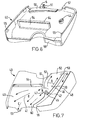
- Fig. 6 shows in perspective view of the antenna body seen from below.
- Fig. 7 shows in perspective view of the antenna body seen from above.
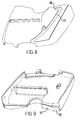
- Fig. 8 shows a first alternative embodiment based on the antenna body shown in fig. 6 and 7.
- Fig. 9 shows a second alternative embodiment based on the antenna body shown in fig. 6 and 7.
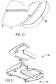
- Fig. 10 shows a third alternative embodiment based on the antenna body shown in fig. 6 and 7.
- Fig. 11 illustrates the two shot mold process for manufacturing the antenna according to the invention.
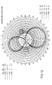
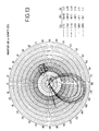
- Fig. 12 and 13 illustrates the radiation pattern for the 900 MHz band and 1800 MHz band, respectively.
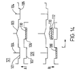
- Fig. 14 (a) and (b) illustrates the preferred steps for performing the injection molding of the antenna according to the antenna.
- Fig. 1 shows a preferred embodiment of a phone according to the invention, and it will be seen that the phone, which is generally designated by 1, comprises a user interface having a keypad 2, a display 3, an on/off button 4, a speaker 5, and a microphone 6 (only openings are shown).
- the phone 1 according to the preferred embodiment is adapted for communication via a cellular network, but could have been designed for a cordless network as well.
- the keypad 2 has a first group 7 of keys as alphanumeric keys, two soft keys 8, two call handling keys 9, and a navigation key 10.
- the present functionality of the soft keys 8 is shown in separate fields in the display 3 just above the keys 8, and the call handling keys 9 are used for establishing a call or a conference call, terminating a call or rejecting an incoming call.
- Fig. 2 schematically shows the most important parts of a preferred embodiment of the phone, said parts being essential to the understanding of the invention.
- the preferred embodiment of the phone of the invention is adapted for use in connection with the GSM 900MHz and GSM 1800 MHz network, but, of course, the invention may also be applied in connection with other phone networks.
- the processor 18 controls the communication with the network via the transmitter/receiver circuit 19 and an antenna 20 that will be discussed in details below.
- the microphone 6 transforms the user's speech into the analog signals formed thereby are A/D converted in an A/D converter (not shown) before the speech is encoded in an audio part 14.
- the encoded speech signal is transferred to the processor 18, which e.g. supports the GSM terminal software.
- the processor 18 also forms the interface to the peripheral units of the apparatus, including a RAM memory 17a and a Flash ROM memory 17b, a SIM card 16, the display 3 and the keypad 2 (as well as data, power supply, etc.).
- the audio part 14 speech-decodes the signal, which is transferred from the processor 18 to the earpiece 5 via a D/A converter (not shown).
- the preferred embodiment of the antenna device according to the invention comprises two basic parts - a shield 24 acting as ground plane for the antenna and a dielectric body 40 coated with a metallic pattern 41 where the latter acts as resonator plane.
- Printed Circuit Board (PCB) 21 carries a plurality of not-shown electric components, and the shield 24 is used as a per se known EMC shielding can for these components.
- the shield 24 is connected along its periphery to the ground of the PCB 21 and the shield 24 is therefore well suited as ground plane for the antenna.
- a resilient metallic leg 23 of a connector 22 is soldered onto the PCB 21 and connects a not shown RX/TX path on the PCB 21 to the antenna body part 40 via connection pin 43 having an internal metallised via 42 coherent with the metallic pattern 41.
- the antenna element will be positioned in the upper rear part of the phone.
- the shield 24 has a number of flanges 25 for guiding the shield relative to the cover of the phone.
- the shield 24 is secured to the PCB 21 by means of screws or the like passing through the holes 30.
- the shield 24 is furthermore provided with a punch out 26 for a not shown SIM card connector.
- the SIM card is placed against the edges of the punch out 26 and secured in this position by not shown locking means.
- a plane area 27 acting as ground plane for the antenna there is provided in the top of the shield 24 a plane area 27 acting as ground plane for the antenna, and this area is also provided with a punch out 29 through which the antenna connector 22 extends.
- the plane area 27 has two resilient spring tongues 28 used for improving the grounding of the antenna along one side (the topside) of the antenna body 40.
- the shield 24 is formed with a step 28 reducing the distance between the ground plane and the resonator plane in this area.
- the antenna body 40 is shown, and from top view (fig. 7) it is seen that the feeding point 42 of the antenna is positioned on the tip of a tongue 45 of the metallic pattern.
- the feeding point 42 is provided as a plated via coming from the rear side of the antenna body 40 and transferring the RF signal between the PCB 21 and the resonator elements of the antenna.
- a metal island 44 surrounds the via on the top of the connection pin 43.
- the shape of the tip of the tongue 45 corresponds to the form of the metal island 44 in order to ease the production.
- the tongue 45 on the metallic pattern 41 is defined in between a main slit 46 and a minor slit 47 branching from the mid one third of the main slit 46.
- the length of the main slit 46, and in particular the circumference, has a substantial influence on the resonance frequency of the two radiating elements 48 and 49 of the antenna.
- the tongue 45 is coherent with the two radiating elements 48 and 49 via a common frequency part 39.
- the two radiating elements 48 and 49 are according to the preferred embodiment dedicated for the GSM 900 MHz band and the 1800 MHz band, respectively.
- the surface currents on the radiating element 48 in the 900 MHz band starts from the feeding point 42 and continues along a broad passage (common frequency part 39) having a rounding 52 which allows the surface current (illustrated by arrows A) to whirl easily around the bottom 53 of the slit 46.
- a rounding 52 which allows the surface current (illustrated by arrows A) to whirl easily around the bottom 53 of the slit 46.
- this rounding 52 increases the gain of the radiating element 48 in the direction normal to the radiation element.
- a capacitive coupling 58 (fig. 6) with the ground plane. This coupling 58 reduces the GSM 900 MHz resonance frequency. When the distance between the termination of the metallic layer and the ground plane is decreased, the capacitive coupling 58 is increased and thereby the GSM 900 MHz resonance frequency is lowered.
- the circumference and thereby the length of the GSM 900 MHz resonator element 48 is determining for the GSM 900 MHz resonance frequency. This circumference of the GSM 900 MHz resonator element 48 does not affect the gain of this element.
- the tip 59 of the resonator element 48 The longer the tip 59 of the resonator element 48 is, the lower the 900 MHz resonance frequency will be. However the tip 59 must not come too close to the point 60 on the 1800 MHz resonator element 49 near the opening of the slit 46 because this will increase the coupling between the two radiating elements and the grounding point adjacent to the opening of the slit 46. If the coupling to ground from the tip 59 is increased the gain of the 900 MHz resonator element 48 will become decreased.
- the length and in particular the circumference of the slit 46 has a substantial influence on the 900 MHz resonance frequency - the longer the slit 46 is, the lower the resonance frequency will be.
- the width of the slit determines both the resonance frequency and the gain.
- a thinner slit 46 gives a higher 900 MHz resonance frequency (partly due to the fact that the circumference is shorter, partly due to the negative coupling of opposite currents) as well as a lower overall gain (due to the negative coupling of the currents running along the two sides of the slit 46.
- the slit 46 will be designed for maximum gain. However it has been observed that a wide slit 46 results in a low resonance frequency and in a slightly lower gain. This might be due to the fact that the minimum width of the resonator element 48 is reduced in order to maintain the overall size of the antenna body. This will affect the ability of the resonator element 48 to guide the surface currents in an effective manner. However the width of the resonator element 48 may then be increased by letting the element 48 have an extension 68 wrapping around the smooth edge of the antenna body. This will lower the resonance frequency of the element 48 due to the increase in circumference, but the gain will be reduced, too. The gain reduction is caused by the fact that the electromagnetic field is kept inside the structure.
- Terminating the slit 46 in a bend portion 66 as shown in fig. 8 may increase the resonance frequency.
- the angle between the main portion 46 and the bend portion 66 will preferably be around 90symbol 176 ⁇ f "Symbol" ⁇ s 12°.
- the slit 46 is continued as a downwardly extending portion 67 into the capacitive coupler 58 as shown in fig. 9. This will reduce the overall gain of the 900 MHz band.
- the surface currents on the radiating element 49 in the 1800 MHz band starts from the feeding point 42 and passes the common frequency part 39 around the end of the second slit 47.
- the second slit 47 increases the bandwidth in the GSM 900 MHz band and reduces the bandwidth in the GSM 1800 MHz band.
- the improvement of the bandwidth in the lower frequency band is higher than the bandwidth reduction in the higher frequency band. It is believed that this is due to the fact that the surface currents have to run in a quite diffuse way - see the arrows B in fig. 7 - and thus resulting in paths having different lengths, which causes the resonator element 49 to resonate at different frequencies in a continuous frequency band.
- This slit 47 has an impact on the bandwidth in the GSM 1800 MHz band.
- a wide slit will reduce the gain of the GSM 900 MHz band resonating element 48. Therefore the slit will be provided with a minimum width in the range 0.8 mm and with a length in the range 4.2 mm.
- This minimum width ensures a minimum coupling between the two resonator elements 48 and 49 and is mainly determined by the manufacturing process where a shot moulding process is used according to the preferred embodiment.
- the length of the slit 47 determines the bandwidth of the 900 MHz band and the gain of the 1800 MHz band. The longer the slit 47 is the higher the bandwidth in the 900 MHz band will be, and the lower the gain in the 1800 MHz band will be.
- a cut 61 decouples the two frequency bands by forcing the 900 MHz current not to run on a capacitive 1800 MHz coupler 54. Reducing the width of the metal pattern between the end of the slit 47 and the cut 61 will have the same effect as increasing the width of the slit 47.
- the 1800 MHz band resonating element 49 is terminated in a shorting surface 56 which is biased toward the shield 24 acting as ground plane for the antenna.
- a metalized pin 51 lowers the resonance frequency of the 1800 MHz band and is moreover used as a gripping arm for attaching the antenna to the shield 24/PCB 21.
- the reason for the resonance frequency lowering is that the surface currents (the arrow C in fig. 6 and 7) can pass around the pin 51 before coming to ground on the rear side of the shield 24 and thus run a longer electrical distance.
- pin 57 similar to the pin 51 is provided for fixing the antenna to the shield 24.
- the pin 57 is not metalised and only serves a mechanical purpose.
- protrusions 55 for establishing snap connection to the shield 24 having similar recesses 65.
- the capacitive coupler 54 is provided as a metallic pattern part on a wall extending towards the shield 24. This coupler 54 reduces the 1800 MHz band resonance frequency - the closer to the ground plane the pattern is terminated the higher coupling there will be and this causes a lower resonance frequency.
- the antenna body 40 as shown in perspective view in fig. 6 and 7, is provided as plastic body in a two shot moulding process.
- the plastic materials used for the two shots needs to have basically specified characteristics - primarily with regard to electrical properties of the antenna body.
- the plastic material or the dielectric material for internal antenna is selected as being a crystalline polymer synthesized from styrene monomer. A surface of such a plastic body may not be coated (plated) with metal while a surface of the same plastic but provided as a compound with an appropriate catalyst may be plated.
- the metallic material will adhere to the compound plastic only and a pattern useful as the strip lines for the antenna may be created.
- Idemitsu Petrochemical Co., Ltd. markets a dielectric material useful for the manufacturing of the antenna body 40 under the trade name XAREC®. According to the preferred embodiment two variants Xarec S-131 (GF 30%) and Xarec SP-150 (GF 30%) are used for the first and second shot, respectively.
- the preferred dielectric material is syndiotactic polystyrene (SPS). Alternative materials having similar properties may be used, e. g. Questra QA 802 or Catalyzed SPS RTP 4699 x 79007.
- the required characteristics for the material in order to be used in an antenna is appropriate electrical properties, such as dielectric constant and loss factor, and an ability to keep these properties for a long time. Basically this requires that the water absorption rate is low in order to secure that the dielectric properties of the antenna remain substantially at the same level. Otherwise the absorbed water will affect the dielectric properties of the antenna body.
- Xarec S-131 (GF 30%) and Xarec SP-150 (GF 30%) have a water absorption/24h at 0,05 % according to the ASTM D 570 test method.
- these dielectric materials may be found from the associated data sheets. However the materials have been selected primarily due to their dielectric constant in the range 3.0-3.1 which affects the relationship between the resonance wave length and the wavelength in free air. Furthermore the water absorption rate is very important because the presence of water in the dielectric material will greatly affect the dielectric properties thereof.
- a method for manufacturing the antenna body 40 as described above will comprise steps of injection moulding followed by plating steps for establishing the required metallic pattern.
- Fig. 14 (a) illustrates the basic steps in the injection moulding process.
- a first step the cavity is created in between a first and a second mould part, 101 and 102 respectively.
- This cavity is created by moving a first tool 120 towards a second tool 121 as shown by the arrow A.
- the first tool 120 has a two identical mold parts (second mold parts 102 and 106), and the second tool 121 has three mold parts (a third mold part 103 and two first mold parts 101 and 105 adjecent thereto).
- the resin is shot (first shot) into the cavity created by the first mold part 101 and the second mold part 102 whereby a first body part 100 is created (the geometrical form of the body is simplyfied in fig.14 (a) and (b) compared with the actual form shown in fig. 11 and fig. 12).
- the resin used for this shot repels metal in a later metalization process.
- the resin is injected through an inlet 104 provided in the first mould part 101.
- the two tools 120 and 121 are separated as indicated by the arrow B in fig.14(b), and the first body part 100 is maintained in the second mould part 102.
- the tool 120 is then displaced so that the second mould part 102 becomes aligned with the central third mould part 103.
- the tools 102 and 103 will form a cavity having the form of the final antenna body part 40 shown in fig. 6 and 7.
- the first body part 100 fills a substantial part of this cavity whereby the residual cavity for receiving the second resin corresponds to the body part 110.
- the tools with the cavity in which the first body part 100 is placed is pre-heated whereby the second resin when shot into the cavity integrates with the first resin body to form a coherent antenna body.
- This coherent body is given the reference number 112.
- the resin used for the second shot allows metal to adhere in a later metalisation process.
- the resin is injected through an inlet 104 provided in the third mould part 103.
- a 10-12 ⁇ m Cu-plating is added to the surface of an antenna body in a pattern defined by the two mould shots.
- the Cu-layer is finally protected by a thin Ni-layer having a thickness around 1-2 ⁇ m.
- the Ni-layer protects the current carrying Cu-layer.
- the part is dipped in a chromate solution in order to passivate the Nickel surface. The metal only adheres to the resin used in the second shot of the injection mold process.
- the first resin is shot into cavity partly defined by one of the second mould parts 102 at the same time as the second resin is shot into cavity partly defined by other of the second mould parts 106. Then the first resin is provided through the outlet 104 in one of the first mould parts 101 and 105, while the second resin is provided through the outlet 104 in the third mould part 103. Only one of the first mould parts 101 and 105 that is aligned with one of the second mould parts 102 and 106 injects resin during a shoot.
- the antenna body described with reference to fig. 3-11 is designed as a dual band antenna for the GSM 900 MHz band and the GSM 1800 MHz band has in the preferred embodiment an overall width around 45 mm, an overall height around 37 mm and overall thickness around 9 mm.
- the overall length of the GSM 900 path 48 is 50-55 mm.
- the overall length of the GSM 1800 MHz path 49 is 20-30 mm.
- Fig. 12 and 13 illustrates the radiation pattern for the 900 MHz band and 1800 MHz band, respectively.
- the S 11 minimum return loss has been measured to - 17 dB for the GSM 900 MHz band and to -34 dB for the GSM 1800 MHz band.
- the maximum gain is 1.6 dBi for the GSM 900 MHz band and 5.2 dBi for the GSM 1800 MHz band, respectively.
- the maximum gain at band edges is 0.8 dBi for the GSM 900 MHz band and 3.23 dBi for the GSM 1800 MHz band, respectively.
- the estimated efficiency at centers is 70 % for the GSM 900 MHz band and 60 % for the GSM 1800 MHz band, respectively.
- the center frequencies are 925 MHz and 1795 MHz, respectively.
- Fig. 12 shows that the power radiated in the GSM 900 MHz band through the rear side of the phone is 1.6 dBi, while the power radiated in the opposite direction is at least 1.6 dB lower.
- Fig. 13 shows that the power radiated in the GSM 1800 MHz band through the rear side of the phone is 5.2 dBi, while the power radiated in the opposite direction is almost negligible.
Abstract
Description
- The invention relates to an antenna for a handset. The antenna includes a metallic plate or layer acting as ground plane for the antenna, a resonator plate or layer acting as radiating element(s), and a feeding point supplying the signal to the antenna. When the ground plane and the resonator plane are electrically coupled the feeding point will be placed in a position where the antenna is matched to the RF output of the handset. Such antennas are known as Plannar Inverted F-Antennas (PIFA).
- Until a few year ago all phones for cellular communication were equipped with an extendable antenna element, as known from e.g. the phone sold under the tradename Nokia 2110TM. Later on this extendable antenna element were substituted by an external helix antenna, as known from e.g. the phone sold under the tradename Nokia 6110TM. Recently the applicant has launched a phone sold under the tradename Nokia 8810TM and this phone includes an internal antenna based on the PIFA concept. The antenna is a so-called single band antenna and the present version it is adapted for GSM in the 900 MHz band (uplink 890-915 MHz and downlink 935-960 MHz). The antenna element will have an electric length corresponding to a quarter wavelength and placing a dielectric between the ground a resonator plane the over physical dimensions is reduced. The overall dimensions of the PIFA are reduced to 32 x 20 x 4 mm.
- WO 95/24746 describes an internal antenna having a dielectric body coated with a metallic layer on two substantially parallel surfaces. This antenna is a single band antenna for the GSM 900 MHz band only. Basically a plastic body is molded and with metal. Afterwards a pattern is created in the metallic layer by removing parts of the coated surfaces by milling. This concept has been used in the phone marketed by Hagenuk under the tradename Global HandyTM.
- US 5.764.190 describes a capacity loaded PIFA according to which an extra plate is interposed in between the ground plane and the radiating element. This requires that a two-shot moulding process is used in addition to several coating processes.
- A letter by C.R. Rowell and R.D. Murch, "A Compact PIFA suitable for dual frequency 900/1800MHz operation", is published in IEEE Transactions on Antennas and Propagation, April 1998,
Volume 46, Number 4. This letter is written by the inventors mentioned in US 5.764.190, and describes further improvement of the three layered antenna concept. The improvement includes providing of a longitudinal slit in the resonator layer in order to obtain two radiating elements. The RF signal is fed to the radiating elements via the intermediate plate. - A letter by Z. D. Lui and P. S. Hall, "Dual-Frequency Planar Inverted-F Antenna", is published in IEEE Transactions on Antennas and Propagation, October 1997,
Volume 45,Number 10. This letter describes a number of solutions - one of these having a rectangular patch for the 900 MHz band. This patch is provided with a L-shaped slot separating one quarter of the 900 MHz band for acting as resonating element in 1800 MHz band. The two resonating elements are interconnected in the bottom of the slot the common feeding point is provided in this interconnection. Furthermore the two resonating elements are shortened in this interconnection by means of a number of shorting pins. Hereby the coupling between the two radiating elements is reduced. - An object of the invention is to provide an antenna for a handset having a form that can be integrated into the per se known handset cabinets. This antenna must be easy to manufacture without the requirement of manual labouring steps.
- This purpose is obtained by the method for manufacturing an antenna body part according to the invention. This purpose is obtained by the method for manufacturing an antenna device according to the invention. A method for manufacturing an antenna device for a radio telephone, comprising steps of providing an antenna body part by forming a first part of the dielectric body by injection molding where a first resin is injected into a first cavity in the injection molding tool, by forming a composite dielectric body by injection molding where a second resin injected into a second cavity in the injection molding tool, said first part of the dielectric body is placed in the second cavity as a core for becoming an integrated part of the composite body, and by coating a metallic layer onto the surface of the composite dielectric body where said first and second resins are selected to have different adhesive properties for the metal coating so one of the resins repels the metallic layer while the other allows the metallic layer to adhere. Finally the antenna body is mounted on a separate metal body acting as ground plane for the antenna body. Hereby the radiating metallic pattern is obtained without using any mask or manually removing of exceeding metallic layer. Actually the antenna body may be handled and any other of the plastic covers of the phone with regard to injection molding. The plating process may be a standard process without any mechanical step as drilling or milling.
- Both resins are selected as being crystalline polymer synthesized from styrene monomer, and one of the resins is provided as a compound with an added catalyst. Hereby the final antenna body will have homogeneous properties and may be manufactured by a standard injection molding process.
- The invention furthermore relates to antenna body part for use in an antenna device using a separate metal shield as ground plane. This antenna body part has a dielectric body, and a first conducting layer acting as resonator plane coated as a pattern covering a part of the dielectric body. This dielectric body is provided by a two shots injection molding process including, wherein the material used in a first shot is a resin repelling metal in a subsequent coating process, and wherein the material used in the second shot is a resin to which metal in the subsequent coating process adhere. The manufacturing process may hereby be a standard two-shot injection molding procedure followed a electroless metallisation process, e.g. a dip plating process, and therefore only requires a very low amount of manual labouring time.
- Preferably the dielectric body is snapped onto the metallic shield acting as ground plane for the antenna. Hereby the shield and the antenna may be handled as one unit during the assembly of the phone.
- By providing the antenna device with a through going bore through the dielectric body a resilient connector on the PCB extending through the shield may be used for feeding the antenna via the connection pad on the rear side of the dielectric body.
- A major purpose of the antenna device according to the invention is to provide an antenna device to be used as in internal antenna for a phone or a handset.
- Fig. 1 schematically illustrates a preferred embodiment of a hand portable phone according to the invention.
- Fig. 2 schematically shows the essential parts of a telephone for communication with a cellular or cordless network.
- Fig. 3 shows in details the antenna feeding concept in cross-section.
- Fig. 4 shows in perspective the antenna body and the metal shield of a phone prior to assembly.
- Fig. 5 shows in plan view of the antenna body and the metal shield when assembled.
- Fig. 6 shows in perspective view of the antenna body seen from below.
- Fig. 7 shows in perspective view of the antenna body seen from above.
- Fig. 8 shows a first alternative embodiment based on the antenna body shown in fig. 6 and 7.
- Fig. 9 shows a second alternative embodiment based on the antenna body shown in fig. 6 and 7.
- Fig. 10 shows a third alternative embodiment based on the antenna body shown in fig. 6 and 7.
- Fig. 11 illustrates the two shot mold process for manufacturing the antenna according to the invention.
- Fig. 12 and 13 illustrates the radiation pattern for the 900 MHz band and 1800 MHz band, respectively.
- Fig. 14 (a) and (b) illustrates the preferred steps for performing the injection molding of the antenna according to the antenna.
- Fig. 1 shows a preferred embodiment of a phone according to the invention, and it will be seen that the phone, which is generally designated by 1, comprises a user interface having a
keypad 2, adisplay 3, an on/off button 4, aspeaker 5, and a microphone 6 (only openings are shown). The phone 1 according to the preferred embodiment is adapted for communication via a cellular network, but could have been designed for a cordless network as well. - According to the preferred embodiment the
keypad 2 has afirst group 7 of keys as alphanumeric keys, twosoft keys 8, two call handling keys 9, and anavigation key 10. The present functionality of thesoft keys 8 is shown in separate fields in thedisplay 3 just above thekeys 8, and the call handling keys 9 are used for establishing a call or a conference call, terminating a call or rejecting an incoming call. - Fig. 2 schematically shows the most important parts of a preferred embodiment of the phone, said parts being essential to the understanding of the invention. The preferred embodiment of the phone of the invention is adapted for use in connection with the GSM 900MHz and GSM 1800 MHz network, but, of course, the invention may also be applied in connection with other phone networks. The
processor 18 controls the communication with the network via the transmitter/receiver circuit 19 and anantenna 20 that will be discussed in details below. - The
microphone 6 transforms the user's speech into the analog signals formed thereby are A/D converted in an A/D converter (not shown) before the speech is encoded in anaudio part 14. The encoded speech signal is transferred to theprocessor 18, which e.g. supports the GSM terminal software. Theprocessor 18 also forms the interface to the peripheral units of the apparatus, including aRAM memory 17a and aFlash ROM memory 17b, aSIM card 16, thedisplay 3 and the keypad 2 (as well as data, power supply, etc.). Theaudio part 14 speech-decodes the signal, which is transferred from theprocessor 18 to theearpiece 5 via a D/A converter (not shown). - As seen from fig. 3, 4 and 5 the preferred embodiment of the antenna device according to the invention comprises two basic parts - a
shield 24 acting as ground plane for the antenna and adielectric body 40 coated with ametallic pattern 41 where the latter acts as resonator plane. Printed Circuit Board (PCB) 21 carries a plurality of not-shown electric components, and theshield 24 is used as a per se known EMC shielding can for these components. Theshield 24 is connected along its periphery to the ground of thePCB 21 and theshield 24 is therefore well suited as ground plane for the antenna. A resilientmetallic leg 23 of aconnector 22 is soldered onto thePCB 21 and connects a not shown RX/TX path on thePCB 21 to theantenna body part 40 viaconnection pin 43 having an internal metallised via 42 coherent with themetallic pattern 41. - The antenna element will be positioned in the upper rear part of the phone.
- As seen from fig. 4 the
shield 24 has a number offlanges 25 for guiding the shield relative to the cover of the phone. Theshield 24 is secured to thePCB 21 by means of screws or the like passing through theholes 30. Theshield 24 is furthermore provided with a punch out 26 for a not shown SIM card connector. The SIM card is placed against the edges of the punch out 26 and secured in this position by not shown locking means. In the top of theshield 24 there is provided aplane area 27 acting as ground plane for the antenna, and this area is also provided with a punch out 29 through which theantenna connector 22 extends. Furthermore theplane area 27 has tworesilient spring tongues 28 used for improving the grounding of the antenna along one side (the topside) of theantenna body 40. Theshield 24 is formed with astep 28 reducing the distance between the ground plane and the resonator plane in this area. - In fig. 6 and 7 the
antenna body 40 is shown, and from top view (fig. 7) it is seen that thefeeding point 42 of the antenna is positioned on the tip of atongue 45 of the metallic pattern. Thefeeding point 42 is provided as a plated via coming from the rear side of theantenna body 40 and transferring the RF signal between thePCB 21 and the resonator elements of the antenna. Ametal island 44 surrounds the via on the top of theconnection pin 43. The shape of the tip of thetongue 45 corresponds to the form of themetal island 44 in order to ease the production. - The
tongue 45 on themetallic pattern 41 is defined in between amain slit 46 and aminor slit 47 branching from the mid one third of themain slit 46. The length of themain slit 46, and in particular the circumference, has a substantial influence on the resonance frequency of the two radiatingelements tongue 45 is coherent with the two radiatingelements common frequency part 39. The two radiatingelements - The surface currents on the radiating
element 48 in the 900 MHz band starts from thefeeding point 42 and continues along a broad passage (common frequency part 39) having a rounding 52 which allows the surface current (illustrated by arrows A) to whirl easily around the bottom 53 of theslit 46. Hereby the distribution of the surface currents becomes more evenly distributed compared to an embodiment having this passage provided with straight parallel edges. It has been observed that this rounding 52 increases the gain of the radiatingelement 48 in the direction normal to the radiation element. - At the end of the
slit 46 there is provided a capacitive coupling 58 (fig. 6) with the ground plane. Thiscoupling 58 reduces the GSM 900 MHz resonance frequency. When the distance between the termination of the metallic layer and the ground plane is decreased, thecapacitive coupling 58 is increased and thereby the GSM 900 MHz resonance frequency is lowered. - The circumference and thereby the length of the GSM 900
MHz resonator element 48 is determining for the GSM 900 MHz resonance frequency. This circumference of the GSM 900MHz resonator element 48 does not affect the gain of this element. - The longer the
tip 59 of theresonator element 48 is, the lower the 900 MHz resonance frequency will be. However thetip 59 must not come too close to thepoint 60 on the 1800MHz resonator element 49 near the opening of theslit 46 because this will increase the coupling between the two radiating elements and the grounding point adjacent to the opening of theslit 46. If the coupling to ground from thetip 59 is increased the gain of the 900MHz resonator element 48 will become decreased. - It has been observed that a constant width of the
slit 46 and a broad ending (the width is increased towards the end) of the 900MHz resonator element 48 gives the highest gain figures. - The length and in particular the circumference of the
slit 46 has a substantial influence on the 900 MHz resonance frequency - the longer theslit 46 is, the lower the resonance frequency will be. - The width of the slit determines both the resonance frequency and the gain. A
thinner slit 46 gives a higher 900 MHz resonance frequency (partly due to the fact that the circumference is shorter, partly due to the negative coupling of opposite currents) as well as a lower overall gain (due to the negative coupling of the currents running along the two sides of theslit 46. - Normally the
slit 46 will be designed for maximum gain. However it has been observed that awide slit 46 results in a low resonance frequency and in a slightly lower gain. This might be due to the fact that the minimum width of theresonator element 48 is reduced in order to maintain the overall size of the antenna body. This will affect the ability of theresonator element 48 to guide the surface currents in an effective manner. However the width of theresonator element 48 may then be increased by letting theelement 48 have anextension 68 wrapping around the smooth edge of the antenna body. This will lower the resonance frequency of theelement 48 due to the increase in circumference, but the gain will be reduced, too. The gain reduction is caused by the fact that the electromagnetic field is kept inside the structure. - Terminating the
slit 46 in abend portion 66 as shown in fig. 8 may increase the resonance frequency. The angle between themain portion 46 and thebend portion 66 will preferably be around 90symbol 176 \f "Symbol" \s 12°. - Alternatively the
slit 46 is continued as a downwardly extending portion 67 into thecapacitive coupler 58 as shown in fig. 9. This will reduce the overall gain of the 900 MHz band. - The surface currents on the radiating
element 49 in the 1800 MHz band starts from thefeeding point 42 and passes thecommon frequency part 39 around the end of thesecond slit 47. Thesecond slit 47 increases the bandwidth in the GSM 900 MHz band and reduces the bandwidth in the GSM 1800 MHz band. However it has been observed that the improvement of the bandwidth in the lower frequency band is higher than the bandwidth reduction in the higher frequency band. It is believed that this is due to the fact that the surface currents have to run in a quite diffuse way - see the arrows B in fig. 7 - and thus resulting in paths having different lengths, which causes theresonator element 49 to resonate at different frequencies in a continuous frequency band. - The width of this slit 47 has an impact on the bandwidth in the GSM 1800 MHz band. The wider the
slit 47 is the lower the bandwidth of the upper frequency band will be. At the same time a wide slit will reduce the gain of the GSM 900 MHzband resonating element 48. Therefore the slit will be provided with a minimum width in the range 0.8 mm and with a length in the range 4.2 mm. This minimum width ensures a minimum coupling between the tworesonator elements slit 47 determines the bandwidth of the 900 MHz band and the gain of the 1800 MHz band. The longer theslit 47 is the higher the bandwidth in the 900 MHz band will be, and the lower the gain in the 1800 MHz band will be. - A
cut 61 decouples the two frequency bands by forcing the 900 MHz current not to run on a capacitive 1800MHz coupler 54. Reducing the width of the metal pattern between the end of theslit 47 and thecut 61 will have the same effect as increasing the width of theslit 47. - The 1800 MHz
band resonating element 49 is terminated in a shortingsurface 56 which is biased toward theshield 24 acting as ground plane for the antenna. A metalizedpin 51 lowers the resonance frequency of the 1800 MHz band and is moreover used as a gripping arm for attaching the antenna to theshield 24/PCB 21. The reason for the resonance frequency lowering is that the surface currents (the arrow C in fig. 6 and 7) can pass around thepin 51 before coming to ground on the rear side of theshield 24 and thus run a longer electrical distance. - Another
pin 57 similar to thepin 51 is provided for fixing the antenna to theshield 24. However thepin 57 is not metalised and only serves a mechanical purpose. In both sides of the antenna body there is providedprotrusions 55 for establishing snap connection to theshield 24 having similar recesses 65. - With reference to fig. 6 it is seen that the
capacitive coupler 54 is provided as a metallic pattern part on a wall extending towards theshield 24. Thiscoupler 54 reduces the 1800 MHz band resonance frequency - the closer to the ground plane the pattern is terminated the higher coupling there will be and this causes a lower resonance frequency. - Basically the
antenna body 40 as shown in perspective view in fig. 6 and 7, is provided as plastic body in a two shot moulding process. According to the preferred embodiment of the invention the plastic materials used for the two shots needs to have basically specified characteristics - primarily with regard to electrical properties of the antenna body. Advantageously the plastic material or the dielectric material for internal antenna is selected as being a crystalline polymer synthesized from styrene monomer. A surface of such a plastic body may not be coated (plated) with metal while a surface of the same plastic but provided as a compound with an appropriate catalyst may be plated. - The metallic material will adhere to the compound plastic only and a pattern useful as the strip lines for the antenna may be created. Idemitsu Petrochemical Co., Ltd. markets a dielectric material useful for the manufacturing of the
antenna body 40 under the trade name XAREC®. According to the preferred embodiment two variants Xarec S-131 (GF 30%) and Xarec SP-150 (GF 30%) are used for the first and second shot, respectively. The preferred dielectric material is syndiotactic polystyrene (SPS). Alternative materials having similar properties may be used, e. g. Questra QA 802 or Catalyzed SPS RTP 4699 x 79007. - The required characteristics for the material in order to be used in an antenna is appropriate electrical properties, such as dielectric constant and loss factor, and an ability to keep these properties for a long time. Basically this requires that the water absorption rate is low in order to secure that the dielectric properties of the antenna remain substantially at the same level. Otherwise the absorbed water will affect the dielectric properties of the antenna body. Xarec S-131 (
GF 30%) and Xarec SP-150 (GF 30%) have a water absorption/24h at 0,05 % according to the ASTM D 570 test method. - Basically the properties of these dielectric materials may be found from the associated data sheets. However the materials have been selected primarily due to their dielectric constant in the range 3.0-3.1 which affects the relationship between the resonance wave length and the wavelength in free air. Furthermore the water absorption rate is very important because the presence of water in the dielectric material will greatly affect the dielectric properties thereof.
- According to the preferred embodiment of the invention a method for manufacturing the
antenna body 40 as described above will comprise steps of injection moulding followed by plating steps for establishing the required metallic pattern. - Fig. 14 (a) illustrates the basic steps in the injection moulding process. As a first step the cavity is created in between a first and a second mould part, 101 and 102 respectively. This cavity is created by moving a
first tool 120 towards asecond tool 121 as shown by the arrow A. Thefirst tool 120 has a two identical mold parts (second mold parts 102 and 106), and thesecond tool 121 has three mold parts (athird mold part 103 and twofirst mold parts first mold part 101 and thesecond mold part 102 whereby afirst body part 100 is created (the geometrical form of the body is simplyfied in fig.14 (a) and (b) compared with the actual form shown in fig. 11 and fig. 12). The resin used for this shot repels metal in a later metalization process. The resin is injected through aninlet 104 provided in thefirst mould part 101. - Then the two
tools first body part 100 is maintained in thesecond mould part 102. Thetool 120 is then displaced so that thesecond mould part 102 becomes aligned with the centralthird mould part 103. Thetools antenna body part 40 shown in fig. 6 and 7. However thefirst body part 100 fills a substantial part of this cavity whereby the residual cavity for receiving the second resin corresponds to thebody part 110. The tools with the cavity in which thefirst body part 100 is placed is pre-heated whereby the second resin when shot into the cavity integrates with the first resin body to form a coherent antenna body. This coherent body is given thereference number 112. The resin used for the second shot allows metal to adhere in a later metalisation process. The resin is injected through aninlet 104 provided in thethird mould part 103. - In plating the plating process, e.g. an electroless dip process, a 10-12 µm Cu-plating is added to the surface of an antenna body in a pattern defined by the two mould shots. The Cu-layer is finally protected by a thin Ni-layer having a thickness around 1-2 µm. The Ni-layer protects the current carrying Cu-layer. Finally the part is dipped in a chromate solution in order to passivate the Nickel surface. The metal only adheres to the resin used in the second shot of the injection mold process.
- By using this lateral displacement of the
tool 120 the first resin is shot into cavity partly defined by one of thesecond mould parts 102 at the same time as the second resin is shot into cavity partly defined by other of thesecond mould parts 106. Then the first resin is provided through theoutlet 104 in one of thefirst mould parts outlet 104 in thethird mould part 103. Only one of thefirst mould parts second mould parts - The antenna body described with reference to fig. 3-11 is designed as a dual band antenna for the GSM 900 MHz band and the GSM 1800 MHz band has in the preferred embodiment an overall width around 45 mm, an overall height around 37 mm and overall thickness around 9 mm. The overall length of the GSM 900
path 48 is 50-55 mm. The overall length of the GSM 1800MHz path 49 is 20-30 mm. - Fig. 12 and 13 illustrates the radiation pattern for the 900 MHz band and 1800 MHz band, respectively. The S11 minimum return loss has been measured to - 17 dB for the GSM 900 MHz band and to -34 dB for the GSM 1800 MHz band. The bandwidth at S11 = -6 dB is 78 MHz (8 MHz excess) for the GSM 900 MHz band and 180 MHz (10 MHz excess) for the GSM 1800 MHz band, respectively.
- The maximum gain is 1.6 dBi for the GSM 900 MHz band and 5.2 dBi for the GSM 1800 MHz band, respectively. The maximum gain at band edges is 0.8 dBi for the GSM 900 MHz band and 3.23 dBi for the GSM 1800 MHz band, respectively. The estimated efficiency at centers is 70 % for the GSM 900 MHz band and 60 % for the GSM 1800 MHz band, respectively. The center frequencies are 925 MHz and 1795 MHz, respectively.
- Fig. 12 shows that the power radiated in the GSM 900 MHz band through the rear side of the phone is 1.6 dBi, while the power radiated in the opposite direction is at least 1.6 dB lower. Fig. 13 shows that the power radiated in the GSM 1800 MHz band through the rear side of the phone is 5.2 dBi, while the power radiated in the opposite direction is almost negligible.
Claims (10)
- A method for manufacturing an antenna device for a radio telephone, comprising steps of:providing an antenna body part by:forming a first part of the dielectric body by injection molding where a first resin is injected into a first cavity in the injection molding tool;forming a composite dielectric body by injection molding where a second resin injected into a second cavity in the injection molding tool, said first part of the dielectric body is placed in the second cavity as a core for becoming an integrated part of the composite body;coating a metallic layer onto the surface of the composite dielectric body where said first and second resins are selected to have different adhesive properties for the metal coating so one of the resins repels the metallic layer while the other allows the metallic layer to adhere; andmounting said antenna body on a separate metal shield acting as ground plane for the antenna body.
- A method according to claim 1, wherein the first and the second resin are selected as being crystalline polymer synthesized from styrene monomer, and wherein either the first and the second resin is provided as a compound with an added catalyst.
- An antenna body part for use in an antenna device using a separate metal shield as ground plane, and having:a dielectric body;a first conducting layer acting as resonator plane coated as a pattern covering a part of the dielectric body; andsaid dielectric body is provided by a two shots injection molding process including, wherein the material used in a first shot is a resin repelling metal in a subsequent coating process, and wherein the material used in the second shot is a resin to which metal in the subsequent coating process adheres.
- An antenna device according to claim 3, wherein the dielectric body is provided with coupling means for establishing a releasable interconnection with a separate metal body acting as the second conducting layer of the device.
- An antenna device according to claim 3, wherein the feeding means includes a bore through the dielectric body as a connection via connecting the first conducting layer to a connection pad on the rear side of the dielectric body.
- A phone or a handset having an internal antenna including:an antenna body part having:a dielectric body;a first conducting layer acting as resonator plane coated as a pattern covering a part of the dielectric body; andsaid dielectric body is provided by a two shots injection moulding process including, wherein the material used in a first shot is a resin repelling metal in a subsequent coating process, and wherein the material used in the second shot is a resin to which metal in the subsequent coating process adheres; anda separate metal shield acting as ground plane for the antenna body.
- A phone or a handset according to claim 6, wherein the dielectric body is provided with coupling means for establishing a releasable interconnection with a separate metal body acting as the second conducting layer of the device.
- A phone or a handset according to claim 6, wherein the feeding means includes a bore through the dielectric body as a connection via connecting the first conducting layer to a connection pad on the rear side of the dielectric body.
- An antenna body part for use in an antenna device using a separate metal shield as ground plane, and having:a dielectric body;a first conducting layer acting as resonator plane coated on the dielectric body; andsaid dielectric body is provided with coupling means for establishing a releasable interconnection with said separate metal shield.
- An antenna body part according to claim 9, wherein said coupling means includes gripping fingers for establishing a snap connection between the antenna body part and the separate metal shield.
Applications Claiming Priority (4)
| Application Number | Priority Date | Filing Date | Title |
|---|---|---|---|
| GB9828364 | 1998-12-22 | ||
| GB9828364A GB2345194B (en) | 1998-12-22 | 1998-12-22 | Dual band antenna for a handset |
| GB9828535 | 1998-12-23 | ||
| GB9828535A GB2345022B (en) | 1998-12-23 | 1998-12-23 | Method for manufacturing an antenna body for a phone |
Publications (2)
| Publication Number | Publication Date |
|---|---|
| EP1020947A2 true EP1020947A2 (en) | 2000-07-19 |
| EP1020947A3 EP1020947A3 (en) | 2000-10-04 |
Family
ID=26314892
Family Applications (1)
| Application Number | Title | Priority Date | Filing Date |
|---|---|---|---|
| EP99310154A Pending EP1020947A3 (en) | 1998-12-22 | 1999-12-16 | Method for manufacturing an antenna body for a phone and phone or handset having an internal antenna |
Country Status (4)
| Country | Link |
|---|---|
| US (1) | US6333716B1 (en) |
| EP (1) | EP1020947A3 (en) |
| JP (1) | JP3615680B2 (en) |
| CN (1) | CN1126190C (en) |
Cited By (13)
| Publication number | Priority date | Publication date | Assignee | Title |
|---|---|---|---|---|
| EP1152481A2 (en) * | 2000-04-20 | 2001-11-07 | Sony Corporation | Antenna device and portable wireless communication apparatus |
| WO2002093683A1 (en) * | 2001-05-16 | 2002-11-21 | Ericsson Inc. | Three-dimensional elastomeric connector |
| WO2003007421A1 (en) * | 2001-07-12 | 2003-01-23 | Moteco Ab | Dual component antenna |
| EP1301011A2 (en) * | 2001-10-05 | 2003-04-09 | Nokia Corporation | User changeable electronic device/mobile phone covers and method |
| EP1388186A1 (en) * | 2001-03-26 | 2004-02-11 | Daniel Luch | Electrically conductive patterns, antennas and methods of manufacture |
| EP1414109A2 (en) * | 2002-10-23 | 2004-04-28 | Centurion Wireless Technologies, Inc. | Dual band single feed dipole antenna and method of making the same |
| EP1441412A1 (en) * | 2003-01-27 | 2004-07-28 | Sony Ericsson Mobile Communications AB | Antenna with distributed ground |
| EP1537626A2 (en) * | 2002-06-18 | 2005-06-08 | Centurion Wireless Technologies, Inc. | Compact dual band circular pifa |
| EP1626422A1 (en) * | 2003-04-25 | 2006-02-15 | Sunarrow Ltd. | Multicolor resin molding component for mobile apparatus |
| US7532164B1 (en) | 2007-05-16 | 2009-05-12 | Motorola, Inc. | Circular polarized antenna |
| EP2517301A1 (en) * | 2009-04-21 | 2012-10-31 | Bayer MaterialScience AG | Three dimensional antenna |
| WO2015054624A1 (en) * | 2013-10-11 | 2015-04-16 | Magna International Inc. | Selective chroming |
| US9246210B2 (en) | 2010-02-18 | 2016-01-26 | Pulse Finland Oy | Antenna with cover radiator and methods |
Families Citing this family (32)
| Publication number | Priority date | Publication date | Assignee | Title |
|---|---|---|---|---|
| US7268774B2 (en) | 1998-08-18 | 2007-09-11 | Candledragon, Inc. | Tracking motion of a writing instrument |
| CN101188325B (en) | 1999-09-20 | 2013-06-05 | 弗拉克托斯股份有限公司 | Multi-level antenna |
| WO2001054225A1 (en) | 2000-01-19 | 2001-07-26 | Fractus, S.A. | Space-filling miniature antennas |
| JP2002314330A (en) | 2001-04-10 | 2002-10-25 | Murata Mfg Co Ltd | Antenna device |
| JP3678167B2 (en) | 2001-05-02 | 2005-08-03 | 株式会社村田製作所 | ANTENNA DEVICE AND RADIO COMMUNICATION DEVICE HAVING THE ANTENNA DEVICE |
| FR2827310B1 (en) * | 2001-07-16 | 2004-07-09 | Cit Alcatel | PROCESS FOR PARTIAL GALVANIZATION OF A PART MADE BY INJECTION MOLDING |
| GB0122226D0 (en) * | 2001-09-13 | 2001-11-07 | Koninl Philips Electronics Nv | Wireless terminal |
| US7257255B2 (en) | 2001-11-21 | 2007-08-14 | Candledragon, Inc. | Capturing hand motion |
| US6834181B2 (en) | 2002-03-13 | 2004-12-21 | Nokia Corporation | Mobile communication device and related construction method |
| US6839029B2 (en) * | 2002-03-15 | 2005-01-04 | Etenna Corporation | Method of mechanically tuning antennas for low-cost volume production |
| US6822609B2 (en) * | 2002-03-15 | 2004-11-23 | Etenna Corporation | Method of manufacturing antennas using micro-insert-molding techniques |
| DE10232947A1 (en) * | 2002-07-19 | 2004-01-29 | Siemens Ag | Container, in particular housing for a mobile telephone part, and method for producing a housing part |
| EP1573856B1 (en) * | 2002-11-28 | 2008-05-28 | Research In Motion Limited | Multiple-band antenna with patch and slot structures |
| US6791500B2 (en) * | 2002-12-12 | 2004-09-14 | Research In Motion Limited | Antenna with near-field radiation control |
| US20040219951A1 (en) * | 2003-04-29 | 2004-11-04 | Holder Helen A | Program controlled apparatus, system and method for remote data messaging and display over an interactive wireless communications network |
| US6885347B2 (en) * | 2003-07-28 | 2005-04-26 | Hon Hai Precision Ind. Co., Ltd. | Method for assembling antenna onto plastic base |
| DE102004046907A1 (en) * | 2004-09-28 | 2006-04-13 | Robert Bosch Gmbh | Antenna housing and method for producing an antenna housing |
| JP4241575B2 (en) * | 2004-11-05 | 2009-03-18 | 日立電線株式会社 | Small antenna |
| US7755026B2 (en) | 2006-05-04 | 2010-07-13 | CandleDragon Inc. | Generating signals representative of sensed light that is associated with writing being done by a user |
| US8738103B2 (en) | 2006-07-18 | 2014-05-27 | Fractus, S.A. | Multiple-body-configuration multimedia and smartphone multifunction wireless devices |
| CN101145633B (en) * | 2007-09-21 | 2013-06-05 | 中兴通讯股份有限公司 | A built-in mobile phone antenna and its making method |
| JP4756020B2 (en) * | 2007-09-25 | 2011-08-24 | 株式会社東芝 | Housing, method for manufacturing the same, and electronic device |
| KR100961137B1 (en) * | 2008-08-05 | 2010-06-09 | 삼성전기주식회사 | Mobile communication terminal case and method of manufacturing the same |
| KR100945123B1 (en) | 2009-04-23 | 2010-03-02 | 삼성전기주식회사 | Antenna pattern frame, method and mould for manufacturing the same,and electronic device |
| US20100289701A1 (en) * | 2009-05-15 | 2010-11-18 | Microsoft Corporation | Antenna configured for bandwidth improvement on a small substrate. |
| WO2011076080A1 (en) * | 2009-12-23 | 2011-06-30 | 北京联想软件有限公司 | Mobile terminal |
| US8508416B2 (en) * | 2010-04-23 | 2013-08-13 | Psion Inc. | Cap assembly |
| CN108417977B (en) * | 2010-10-06 | 2020-08-07 | 诺基亚技术有限公司 | Antenna apparatus and method |
| WO2013045977A1 (en) * | 2011-09-28 | 2013-04-04 | Nokia Corporation | Apparatus and methods of forming molded parts |
| CN103029259B (en) | 2011-09-30 | 2015-11-25 | 苹果公司 | For the injection-molded instrument removed with integrated cast gate of large-scale production |
| US10737530B2 (en) * | 2015-05-14 | 2020-08-11 | Lacks Enterprises, Inc. | Two-shot molding for selectively metalizing parts |
| US20200280120A1 (en) | 2019-03-01 | 2020-09-03 | Microsoft Technology Licensing, Llc | High Frequency Antenna Integration in Electronic Devices |
Citations (3)
| Publication number | Priority date | Publication date | Assignee | Title |
|---|---|---|---|---|
| US4812275A (en) | 1986-11-18 | 1989-03-14 | Sankyo Kasei Kabushiki Kaisha | Process for the production of molded articles having partial metal plating |
| US4908259A (en) | 1986-11-18 | 1990-03-13 | Sankyo Kasei Kabushiki Kaisha | Molded article with partial metal plating and a process for producing such article |
| JPH09232855A (en) | 1996-02-20 | 1997-09-05 | Mitsubishi Electric Corp | Electronic component |
Family Cites Families (16)
| Publication number | Priority date | Publication date | Assignee | Title |
|---|---|---|---|---|
| DD111932A1 (en) * | 1974-06-05 | 1975-03-12 | ||
| GB2171355B (en) | 1985-02-22 | 1989-11-22 | Kollmorgen Tech Corp | Molded articles suitable for adherent metallization, molded metallized articles and processes for making the same |
| US5407622A (en) * | 1985-02-22 | 1995-04-18 | Smith Corona Corporation | Process for making metallized plastic articles |
| JPS6223603A (en) * | 1985-03-27 | 1987-01-31 | Furukawa Electric Co Ltd:The | Manufacture of primary radiator |
| IN167760B (en) | 1986-08-15 | 1990-12-15 | Kollmorgen Tech Corp | |
| ATE130859T1 (en) * | 1989-03-20 | 1995-12-15 | Idemitsu Kosan Co | STYRENE COPOLYMER AND METHOD FOR PRODUCTION. |
| JPH02307716A (en) * | 1989-05-23 | 1990-12-20 | Dynic Corp | Synthetic resin plate, molding method thereof and plate-like core for molding thereof |
| FR2699740B1 (en) | 1992-12-23 | 1995-03-03 | Patrice Brachat | Broadband antenna with reduced overall dimensions, and corresponding transmitting and / or receiving device. |
| AU1892895A (en) * | 1994-03-08 | 1995-09-25 | Hagenuk Telecom Gmbh | Hand-held transmitting and/or receiving apparatus |
| FR2718292B1 (en) | 1994-04-01 | 1996-06-28 | Christian Sabatier | Antenna for transmitting and / or receiving electromagnetic signals, in particular microwave frequencies, and device using such an antenna. |
| FR2721733B1 (en) * | 1994-06-22 | 1996-08-23 | Gemplus Card Int | Method for manufacturing a contactless card by overmolding and contactless card obtained by such a method. |
| US5764190A (en) * | 1996-07-15 | 1998-06-09 | The Hong Kong University Of Science & Technology | Capacitively loaded PIFA |
| WO1999035708A1 (en) * | 1998-01-05 | 1999-07-15 | The Furukawa Electric Co., Ltd. | Antenna device for portable telephone, and method of manufacture |
| US6040803A (en) * | 1998-02-19 | 2000-03-21 | Ericsson Inc. | Dual band diversity antenna having parasitic radiating element |
| US6097339A (en) * | 1998-02-23 | 2000-08-01 | Qualcomm Incorporated | Substrate antenna |
| US6110576A (en) * | 1998-10-16 | 2000-08-29 | Lucent Technologies Inc. | Article comprising molded circuit |
-
1999
- 1999-12-16 EP EP99310154A patent/EP1020947A3/en active Pending
- 1999-12-21 JP JP36264799A patent/JP3615680B2/en not_active Expired - Fee Related
- 1999-12-21 CN CN99126924A patent/CN1126190C/en not_active Expired - Lifetime
- 1999-12-22 US US09/469,895 patent/US6333716B1/en not_active Expired - Lifetime
Patent Citations (4)
| Publication number | Priority date | Publication date | Assignee | Title |
|---|---|---|---|---|
| US4812275A (en) | 1986-11-18 | 1989-03-14 | Sankyo Kasei Kabushiki Kaisha | Process for the production of molded articles having partial metal plating |
| US4908259A (en) | 1986-11-18 | 1990-03-13 | Sankyo Kasei Kabushiki Kaisha | Molded article with partial metal plating and a process for producing such article |
| US5015519A (en) | 1986-11-18 | 1991-05-14 | Sankyo Kasei Kabushiki Kaisha | Molded article with partial metal plating and a process for producing such article |
| JPH09232855A (en) | 1996-02-20 | 1997-09-05 | Mitsubishi Electric Corp | Electronic component |
Cited By (21)
| Publication number | Priority date | Publication date | Assignee | Title |
|---|---|---|---|---|
| EP1152481A2 (en) * | 2000-04-20 | 2001-11-07 | Sony Corporation | Antenna device and portable wireless communication apparatus |
| EP1152481A3 (en) * | 2000-04-20 | 2002-10-09 | Sony Corporation | Antenna device and portable wireless communication apparatus |
| EP1388186A1 (en) * | 2001-03-26 | 2004-02-11 | Daniel Luch | Electrically conductive patterns, antennas and methods of manufacture |
| EP1388186A4 (en) * | 2001-03-26 | 2005-08-17 | Daniel Luch | Electrically conductive patterns, antennas and methods of manufacture |
| WO2002093683A1 (en) * | 2001-05-16 | 2002-11-21 | Ericsson Inc. | Three-dimensional elastomeric connector |
| WO2003007421A1 (en) * | 2001-07-12 | 2003-01-23 | Moteco Ab | Dual component antenna |
| EP1301011A2 (en) * | 2001-10-05 | 2003-04-09 | Nokia Corporation | User changeable electronic device/mobile phone covers and method |
| EP1301011A3 (en) * | 2001-10-05 | 2009-03-25 | Nokia Corporation | User changeable electronic device/mobile phone covers and method |
| EP1537626A4 (en) * | 2002-06-18 | 2005-07-13 | Centurion Wireless Tech Inc | Compact dual band circular pifa |
| EP1537626A2 (en) * | 2002-06-18 | 2005-06-08 | Centurion Wireless Technologies, Inc. | Compact dual band circular pifa |
| EP1414109A3 (en) * | 2002-10-23 | 2005-01-26 | Centurion Wireless Technologies, Inc. | Dual band single feed dipole antenna and method of making the same |
| EP1414109A2 (en) * | 2002-10-23 | 2004-04-28 | Centurion Wireless Technologies, Inc. | Dual band single feed dipole antenna and method of making the same |
| EP1441412A1 (en) * | 2003-01-27 | 2004-07-28 | Sony Ericsson Mobile Communications AB | Antenna with distributed ground |
| EP1626422A1 (en) * | 2003-04-25 | 2006-02-15 | Sunarrow Ltd. | Multicolor resin molding component for mobile apparatus |
| EP1626422A4 (en) * | 2003-04-25 | 2007-08-08 | Sunarrow Ltd | Multicolor resin molding component for mobile apparatus |
| US7532164B1 (en) | 2007-05-16 | 2009-05-12 | Motorola, Inc. | Circular polarized antenna |
| EP2517301A1 (en) * | 2009-04-21 | 2012-10-31 | Bayer MaterialScience AG | Three dimensional antenna |
| EP2517301A4 (en) * | 2009-04-21 | 2013-07-31 | Bayer Ip Gmbh | Three dimensional antenna |
| US9246210B2 (en) | 2010-02-18 | 2016-01-26 | Pulse Finland Oy | Antenna with cover radiator and methods |
| WO2015054624A1 (en) * | 2013-10-11 | 2015-04-16 | Magna International Inc. | Selective chroming |
| US10822711B2 (en) | 2013-10-11 | 2020-11-03 | Magna International Inc. | Selective chroming |
Also Published As
| Publication number | Publication date |
|---|---|
| US6333716B1 (en) | 2001-12-25 |
| CN1261211A (en) | 2000-07-26 |
| CN1126190C (en) | 2003-10-29 |
| JP2000196326A (en) | 2000-07-14 |
| EP1020947A3 (en) | 2000-10-04 |
| JP3615680B2 (en) | 2005-02-02 |
Similar Documents
| Publication | Publication Date | Title |
|---|---|---|
| US6333716B1 (en) | Method for manufacturing an antenna body for a phone | |
| US6271794B1 (en) | Dual band antenna for a handset | |
| EP1020948B1 (en) | Dual band antenna for a hand portable telephone and a corresponding hand portable telephone | |
| US9246210B2 (en) | Antenna with cover radiator and methods | |
| AU750257B2 (en) | Multiple frequency band antenna | |
| US7876273B2 (en) | Apparatus and method | |
| EP2223381B1 (en) | Apparatus and methods for wireless communication | |
| US6646610B2 (en) | Antenna | |
| US8537072B2 (en) | Antenna for mobile terminal unit | |
| US7012571B1 (en) | Multiple ground plane section antenna systems and methods | |
| KR20010020104A (en) | Asymmetric dipole antenna assembly | |
| US6597319B2 (en) | Antenna device for a communication terminal | |
| US6392605B2 (en) | Antenna for a handset | |
| GB2345022A (en) | Method for manufacturing an antenna body for a phone | |
| EP1634349B1 (en) | Built-in antenna having center feeding structure for wireless terminal | |
| GB2345195A (en) | Dual band antenna for a handset | |
| KR20080025622A (en) | Antenna apparatus for portable terminal |
Legal Events
| Date | Code | Title | Description |
|---|---|---|---|
| PUAI | Public reference made under article 153(3) epc to a published international application that has entered the european phase |
Free format text: ORIGINAL CODE: 0009012 |
|
| AK | Designated contracting states |
Kind code of ref document: A2 Designated state(s): DE FR IT SE |
|
| AX | Request for extension of the european patent |
Free format text: AL;LT;LV;MK;RO;SI |
|
| PUAL | Search report despatched |
Free format text: ORIGINAL CODE: 0009013 |
|
| AK | Designated contracting states |
Kind code of ref document: A3 Designated state(s): AT BE CH CY DE DK ES FI FR GB GR IE IT LI LU MC NL PT SE |
|
| AX | Request for extension of the european patent |
Free format text: AL;LT;LV;MK;RO;SI |
|
| 17P | Request for examination filed |
Effective date: 20010404 |
|
| AKX | Designation fees paid |
Free format text: DE FR IT SE |
|
| TPAD | Observations filed by third parties |
Free format text: ORIGINAL CODE: EPIDOS TIPA |
|
| 17Q | First examination report despatched |
Effective date: 20010608 |
|
| RAP1 | Party data changed (applicant data changed or rights of an application transferred) |
Owner name: NOKIA CORPORATION |
|
| 17Q | First examination report despatched |
Effective date: 20010608 |
|
| 18R | Application refused |
Effective date: 20080703 |
|
| D18D | Application deemed to be withdrawn (deleted) | ||
| STAA | Information on the status of an ep patent application or granted ep patent |
Free format text: STATUS: THE APPLICATION HAS BEEN REFUSED |
|
| R18R | Application refused (corrected) |
Effective date: 20080610 |