EP1006368A2 - Opto-electronic sensor and process for manufacture of same - Google Patents
Opto-electronic sensor and process for manufacture of same Download PDFInfo
- Publication number
- EP1006368A2 EP1006368A2 EP99119450A EP99119450A EP1006368A2 EP 1006368 A2 EP1006368 A2 EP 1006368A2 EP 99119450 A EP99119450 A EP 99119450A EP 99119450 A EP99119450 A EP 99119450A EP 1006368 A2 EP1006368 A2 EP 1006368A2
- Authority
- EP
- European Patent Office
- Prior art keywords
- injection
- optical
- electronic components
- housing
- components
- Prior art date
- Legal status (The legal status is an assumption and is not a legal conclusion. Google has not performed a legal analysis and makes no representation as to the accuracy of the status listed.)
- Withdrawn
Links
Images

Classifications
-
- G—PHYSICS
- G01—MEASURING; TESTING
- G01S—RADIO DIRECTION-FINDING; RADIO NAVIGATION; DETERMINING DISTANCE OR VELOCITY BY USE OF RADIO WAVES; LOCATING OR PRESENCE-DETECTING BY USE OF THE REFLECTION OR RERADIATION OF RADIO WAVES; ANALOGOUS ARRANGEMENTS USING OTHER WAVES
- G01S7/00—Details of systems according to groups G01S13/00, G01S15/00, G01S17/00
- G01S7/48—Details of systems according to groups G01S13/00, G01S15/00, G01S17/00 of systems according to group G01S17/00
- G01S7/481—Constructional features, e.g. arrangements of optical elements
- G01S7/4811—Constructional features, e.g. arrangements of optical elements common to transmitter and receiver
-
- G—PHYSICS
- G01—MEASURING; TESTING
- G01V—GEOPHYSICS; GRAVITATIONAL MEASUREMENTS; DETECTING MASSES OR OBJECTS; TAGS
- G01V8/00—Prospecting or detecting by optical means
- G01V8/10—Detecting, e.g. by using light barriers
Definitions
- the invention relates to an opto-electronic sensor with in a housing arranged optical and electronic components and a Method of manufacturing such a sensor.
- the plastic mass used for the housing and optical components is preferably at least partially transparent to visible light, UV radiation or infrared radiation, depending on the type of each to be manufactured Sensors.
- the stated property of the plastic mass enables the latter the imaging necessary for the realization of the optical components To give properties.
- the plastic mass for example be designed as an optical filter, so that they ultimately a Triple function as a lens, filter and housing can perform.
- the process according to the invention is preferably carried out in such a way that the electronic components before the injection or casting process on one Board arranged and then the board in a precise position Injection or casting tool is inserted, whereupon the injection or Casting process can take place.
- the positioning of the board in the spray or Casting tool can advantageously by provided in the board Positioning holes and associated positioning pins in the injection or casting tool can be simplified.
- these sensors can either be outside the injection or casting tool or be isolated within this tool, the latter If the separation is preferred by means of a punching process he follows.
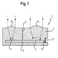
- Fig. 1 shows a sensor 1 with a flat, perpendicular to the plane of the drawing extending circuit board 2, arranged on the electronic components are. These electronic components are shown in FIG. 1 For the sake of clarity, only one light transmitter 3 and one light receiver 4 drawn. Other electronic components can also be found on the board 2, but are not shown in Fig. 1.
- a socket 6 is provided on a narrow side 5 of the circuit board 2, via which the sensor 1 with supply, control and / or data lines can be coupled.
- the socket 6 could for example also on the Bottom of the board 2 may be provided.
- Fig. 2a shows a flat element - often referred to as "benefit" 10, which comprises a plurality of boards 2.
- 2a are exemplary only three boards 2 drawn.
- Each board 2 carries all electronic Components that are necessary to implement a single sensor.
- the individual boards 2 are in the flat element 10 via thin webs 12 held so that between the flat element 10 and the boards 2, an air gap 13 is formed, which apart from minor interruptions through the webs 12 almost over the full extent of the respective boards 2 extends.
- This air gap 13 makes an almost complete one Injection molding or casting around the boards 2 possible.
- the boards 2 are thus with one another via the webs 12 and the element 10 connected within a common plane and relative to each other unchangeably adjusted.
- each Cavity has the negative form of a sensor to be manufactured including the negative form of the optical components to be formed.
- the individual sensors can 1 separated from each other by means of a suitable work step as shown in Fig. 2c.
Abstract
Description
Die Erfindung betrifft einen opto-elektronischen Sensor mit in einem Gehäuse angeordneten optischen und elektronischen Bauteilen sowie ein Verfahren zur Herstellung eines solchen Sensors.The invention relates to an opto-electronic sensor with in a housing arranged optical and electronic components and a Method of manufacturing such a sensor.
Es ist bekannt, die optischen und elektronischen Bauteile der genannten Sensoren in einem Gehäuse anzuordnen und zu fixieren und das Gehäuse anschließend mittels eines Deckels zu verschließen. Weiterhin ist es bekannt, die elektronischen und optischen Bauteile beispielsweise auf einer Platine anzuordnen und diese Platine dann gemeinsam mit den optischen und elektronischen Bauteilen mit Kunststoffmasse zu umspritzen, wobei die Kunststoffmasse in diesem Fall das Gehäuse bildet.It is known the optical and electronic components of the above Arrange sensors in a housing and fix and the housing then close with a lid. Furthermore, it is known the electronic and optical components, for example, on one Arrange board and then this board together with the optical and encapsulate electronic components with plastic compound, wherein the plastic mass in this case forms the housing.
Die Herstellung derartiger, bekannter Sensoren ist auf nachteilige Weise mit hohem Aufwand verbunden, da Elektronik und Optik in Form von separaten Bauteilen positioniert und justiert werden müssen und das Gehäuse - sowohl als mittels eines Deckels verschließbares Element als auch als Kunststoffmasse - ein weiteres separates Bauteil bildet.The production of such known sensors is disadvantageous connected with a lot of effort because electronics and optics in the form of separate Components must be positioned and adjusted and the housing - Both as a closable element by means of a lid as well as a plastic mass - forms another separate component.
Eine Aufgabe der vorliegenden Erfindung besteht darin, die Herstellungskosten von Sensoren der eingangs genannten Art zu reduzieren, insbesondere durch Verringerung der Anzahl der miteinander zu verbindenden Bauteile.An object of the present invention is the manufacturing cost to reduce sensors of the type mentioned, in particular by reducing the number of interconnected Components.
Diese Aufgabe wird durch einen erfindungsgemäßen Sensor dadurch gelöst, daß sowohl das Gehäuse als auch die optischen Bauteile aus einer einheitlichen Kunststoffmasse gebildet sind, welche die elektronischen Bauteile einbettend umschließt.This object is achieved by a sensor according to the invention that both the housing and the optical components from one uniform plastic mass are formed, which the electronic Embedding components.
Gemäß einem erfindungsgemäßen Verfahren wird die genannte Aufgabe dadurch gelöst, daß sowohl das Gehäuse als auch die optischen Bauteile durch einen einzigen, gemeinsamen Spritz- oder Gießvorgang aus einer einheitlichen Kunststoffmasse gefertigt werden, wobei die elektronischen Bauteile mittels des Spritz- oder Gießvorgangs in der Kunststoffmasse eingebettet werden.According to a method according to the invention, the stated object solved in that both the housing and the optical components through a single, common injection or casting process from one uniform plastic mass are manufactured, the electronic Components by means of the injection or pouring process in the plastic mass be embedded.
Erfindungsgemäß bestehen also sowohl die elektronischen Bauteile als auch das Gehäuse aus dem gleichen Kunststoffmaterial, wobei diesem Kunststoffmaterial sowohl hinsichtlich der optischen Bauteile als auch hinsichtlich des Gehäuses seine endgültige Form mittels eines einzigen, gemeinsamen Spritz- oder Gießvorgangs verliehen wird.According to the invention, there are both the electronic components and also the housing from the same plastic material, this Plastic material both in terms of optical components as well the final shape of the housing by means of a single, joint injection or casting process is awarded.
Zur Herstellung eines erfindungsgemäßen Sensors ist es folglich nur noch nötig, die elektronischen Bauteile in einem Spritz- bzw. Gießwerkzeug zu positionieren, woraufhin der Spritz- oder Gießvorgang erfolgt, durch den die optischen Bauteile und das Gehäuse gebildet und mit den elektronischen Bauteilen verbunden werden. Das Herstellungsverfahren ist somit auf einen Positioniervorgang der elektronischen Bauteile in einer Spritz- bzw. Gießform und einen nachfolgenden Spritz- bzw. Gießvorgang reduziert, wodurch sich die Herstellungskosten von Sensoren der eingangs genannten Art erheblich verringern lassen.It is therefore only necessary to manufacture a sensor according to the invention necessary to close the electronic components in an injection or casting tool position, whereupon the injection or pouring process takes place through the the optical components and the housing formed and with the electronic Components are connected. The manufacturing process is thus on a positioning process of the electronic components in a spray or Mold and a subsequent injection or casting process reduced, whereby the manufacturing costs of sensors of the aforementioned Have the species significantly reduced.
Zusätzlich zu der genannten Verringerung der Herstellungskosten ergeben sich erfindungsgemäß noch eine Reihe von weiteren Vorteilen:
- Zur Herstellung von flüssigkeits- oder gasdichten Sensoren ist es nicht mehr nötig, die optischen Bauteile gegenüber dem Gehäuse abzudichten, da diese optischen Bauteile und das Gehäuse einstückig aus einer einheitlichen Kunststoffmasse geformt sind.
- Zwischen einem Lichtsender bzw. einem Lichtempfänger und dem Gehäuse ist ein besonders guter Wärmeübergang gegeben, da die Kunststoffmasse zum einen direkt am Lichtsender bzw. Lichtempfänger und zum anderen direkt am Gehäuse anliegen kann, so daß die Kunststoffmasse Wärme von Lichtsender bzw. Lichtempfänger zur Gehäuseoberfläche leiten kann, ohne daß zwischen den genannten Bauteilen störende Luftspalte vorhanden wären.
- Positionierungs- und Justierungsungenauigkeiten zwischen optischen Bauteilen und Gehäuse werden ausgeschlossen, da die Relativposition von optischen Bauteilen und Gehäuse durch die Gestalt des Spritz- bzw. Gießwerkzeugs fest und unveränderlich vorgegeben ist.
- For the production of liquid- or gas-tight sensors, it is no longer necessary to seal the optical components with respect to the housing, since these optical components and the housing are formed in one piece from a uniform plastic mass.
- A particularly good heat transfer is provided between a light transmitter or a light receiver and the housing, since the plastic mass can lie directly on the light transmitter or light receiver and directly on the housing, so that the plastic mass conducts heat from the light transmitter or light receiver to the housing surface can without disturbing air gaps between the components mentioned.
- Positioning and adjustment inaccuracies between optical components and housing are excluded, since the relative position of optical components and housing is fixed and unchangeable by the shape of the injection or casting tool.
Die für Gehäuse und optische Bauteile verwendete Kunststoffmasse ist vorzugsweise zumindest teilweise durchlässig für sichtbares Licht, UV-Strahlung oder Infrarotstrahlung, je nach Typ des jeweils herzustellenden Sensors. Die genannte Eigenschaft der Kunststoffmasse ermöglicht es, dieser die für die Realisierung der optischen Bauteile nötigen abbildenden Eigenschaften zu verleihen. Zudem kann die Kunststoffmasse beispielsweise als optisches Filter ausgebildet werden, so daß sie letztlich eine Dreifachfunktion als Linse, Filter und Gehäuse erfüllen kann.The plastic mass used for the housing and optical components is preferably at least partially transparent to visible light, UV radiation or infrared radiation, depending on the type of each to be manufactured Sensors. The stated property of the plastic mass enables the latter the imaging necessary for the realization of the optical components To give properties. In addition, the plastic mass, for example be designed as an optical filter, so that they ultimately a Triple function as a lens, filter and housing can perform.
Von Vorteil ist es, wenn die elektronischen Bauelemente mit einem Kabel, einem Stecker und/oder einer Buchse gekoppelt sind, wobei Kabel, Stecker und/oder Buchse zumindest teilweise in der Kunststoffmasse eingebettet sind. Auf diese Weise ergibt sich beim Spritz- bzw. Gießvorgang automatisch eine Fixierung von Kabel, Stecker und/oder Buchse, wenn diese zuvor in das Spritz- bzw. Gießwerkzeug eingelegt wurden. Beim Einbetten eines Kabels ist es dabei von Vorteil, daß sich automatisch eine Zugentlastung ergibt.It is advantageous if the electronic components with a cable, a plug and / or a socket are coupled, cables, plugs and / or socket at least partially embedded in the plastic mass are. This results in the injection or casting process automatically fixes the cable, plug and / or socket if these were previously placed in the injection or casting tool. When embedding a cable, it is advantageous that automatically Strain relief results.
Das erfindungsgemäße Verfahren wird bevorzugt derart durchgeführt, daß die elektronischen Bauteile vor dem Spritz- bzw. Gießvorgang auf einer Platine angeordnet und die Platine anschließend positionsgenau in ein Spritz- bzw. Gießwerkzeug eingelegt wird, woraufhin dann der Spritz- bzw. Gießvorgang erfolgen kann. Die Positionierung der Platine im Spritz- bzw. Gießwerkzeug kann auf vorteilhafte Weise durch in der Platine vorgesehene Positionierungsbohrungen und damit zusammenwirkende Positionierungszapfen im Spritz- bzw. Gießwerkzeug vereinfacht werden.The process according to the invention is preferably carried out in such a way that the electronic components before the injection or casting process on one Board arranged and then the board in a precise position Injection or casting tool is inserted, whereupon the injection or Casting process can take place. The positioning of the board in the spray or Casting tool can advantageously by provided in the board Positioning holes and associated positioning pins in the injection or casting tool can be simplified.
Von besonderem Vorteil ist es, wenn zur gleichzeitigen Herstellung einer Mehrzahl von Sensoren mehrere, miteinander verbundene, jeweils einem Sensor zugeordnete Platinen in einem einzigen Verfahrensschritt mit Kunststoffmasse umspritzt oder umgossen werden. Das Spritz- bzw. Gießwerkzeug muß in diesem Fall dann eine entsprechende Anzahl von Kavitäten zur Herstellung der Sensoren aufweisen.It is of particular advantage if a Plurality of sensors, several, each connected to one another Sensor-assigned boards in a single process step Plastic compound is overmolded or cast. The spray or In this case, the casting tool must have a corresponding number of Have cavities for the production of the sensors.
Im Anschluß an die genannte gleichzeitige Herstellung mehrerer Sensoren können diese Sensoren entweder außerhalb des Spritz- oder Gießwerkzeugs oder innerhalb dieses Werkzeugs vereinzelt werden, wobei im letztgenannten Fall die Vereinzelung bevorzugt mittels eines Stanzvorgangs erfolgt.Following the aforementioned simultaneous production of several sensors these sensors can either be outside the injection or casting tool or be isolated within this tool, the latter If the separation is preferred by means of a punching process he follows.
Weitere bevorzugte Ausführungsformen sind in den Unteransprüchen angegeben.Further preferred embodiments are specified in the subclaims.
Die Erfindung wird nachfolgend anhand von Beispielen unter Bezugnahme auf die Zeichnungen beschrieben; diese zeigen:
- Fig. 1
- einen Schnitt durch einen erfindungsgemäßen Sensor und
- Fig. 2a-c
- drei Verfahrensschritte bei der gleichzeitigen Herstellung mehrerer Sensoren.
- Fig. 1
- a section through a sensor according to the invention and
- 2a-c
- three process steps in the simultaneous production of several sensors.
Fig. 1 zeigt einen Sensor 1 mit einer flächigen, sich senkrecht zur Zeichenebene
erstreckenden Platine 2, auf der elektronische Bauelemente angeordnet
sind. Von diesen elektronischen Bauelementen sind in Fig. 1 aus
Gründen der Übersichtlichkeit lediglich ein Lichtsender 3 sowie ein Lichtempfänger
4 gezeichnet. Weitere elektronische Bauteile finden sich ebenfalls
auf der Platine 2, sind jedoch in Fig. 1 nicht dargestellt. Fig. 1 shows a
Zwischen Lichtsender 3 und Lichtempfänger 4 erstreckt sich senkrecht
zur Platine 2 eine optisch undurchlässige Trennplatte 11, welche Lichtsender
3 und Lichtempfänger 4 optisch voneinander entkoppelt.Extends vertically between light transmitter 3 and light receiver 4
to the
An einer Schmalseite 5 der Platine 2 ist eine Buchse 6 vorgesehen, über
welche der Sensor 1 mit Versorgungs-, Steuer- und/oder Datenleitungen
koppelbar ist. Alternativ könnte die Buchse 6 beispielsweise auch an der
Unterseite der Platine 2 vorgesehen sein.A
Platine 2, Lichtsender 3, Lichtempfänger 4, Buchse 6 und Trennplatte 11
sind mit einer lichtdurchlässigen Kunststoffmasse 7 umspritzt, wobei diese
Kunststoffmasse 7 sowohl das Gehäuse des Sensors 1 als auch die
oberhalb des Lichtsenders 3 angeordnete Sendeoptik 8 und die oberhalb
des Lichtempfängers 4 angeordnete Empfangsoptik 9 bildet.
Aus der Darstellung gemäß Fig. 1 wird deutlich, daß die Kunststoffmasse
7 unmittelbar an Lichtsender 3 und Lichtempfänger 4 anschließt, woraus
sich die vorstehend erläuterten Vorteile ergeben.1 that the
Fig. 2a zeigt ein - oftmals als "Nutzen" bezeichnetes - flächiges Element
10, welches eine Vielzahl von Platinen 2 umfaßt. In Fig. 2a sind beispielhaft
lediglich drei Platinen 2 gezeichnet. Jede Platine 2 trägt alle elektronischen
Bauteile, die zur Realisierung eines einzelnen Sensors nötig sind.Fig. 2a shows a flat element - often referred to as "benefit"
10, which comprises a plurality of
Die einzelnen Platinen 2 sind im flächigen Element 10 über dünne Stege
12 gehalten, so daß zwischen dem flächigen Element 10 und den Platinen
2 ein Luftspalt 13 ausgebildet ist, welcher sich bis auf geringfügige Unterbrechungen
durch die Stege 12 fast über den vollständigen Umfang der
jeweiligen Platinen 2 erstreckt. Dieser Luftspalt 13 macht ein fast vollständiges
Umspritzen bzw. Umgießen der Platinen 2 möglich.The
Die Platinen 2 sind somit über die Stege 12 und das Element 10 miteinander
innerhalb einer gemeinsamen Ebene verbunden und relativ zueinander
unveränderlich justiert.The
Zur gleichzeitigen Herstellung mehrerer erfindungsgemäßer Sensoren wird
das Element 10 in ein das gesamte Element 10 umschließendes Spritz- bzw.
Gießwerkzeug eingelegt, wobei letzteres eine Anzahl von Kavitäten
aufweist, die der Anzahl der herzustellenden Sensoren entspricht. Jede
Kavität besitzt die Negativform eines herzustellenden Sensors einschließlich
der Negativform der zu bildenden optischen Bauteile.For the simultaneous production of several sensors according to the invention
the
Durch einen einzigen Spritzvorgang werden sämtliche Platinen 2 des Elements
10 mit Kunststoffmasse umspritzt bzw. umgossen, wodurch die
Gehäuse und optischen Bauelemente aller herzustellenden Sensoren
gleichzeitig geschaffen werden.Through a single injection process, all of the element's
Bevorzugt ist es, wenn ein etwaiger, nach dem Spritz- bzw. Gießvorgang auftretender Schwund der Kunststoffmasse bereits bei Anfertigung der Spritz- bzw. Gießwerkzeuge berücksichtigt wird, so daß die Sensoren und insbesondere deren optischen Bauteile letztlich die jeweils gewünschten Abmessungen aufweisen.It is preferred if any, after the injection or casting process shrinkage of the plastic mass already occurring when the Injection molding or casting tools is taken into account, so that the sensors and especially their optical components ultimately the desired ones Have dimensions.
Nach dem Spritz- bzw. Gießvorgang ist auf dem Element 10 die gewünschte
Anzahl von Sensoren 1 vorhanden, deren Gehäuse, Sendeoptiken
8 und Empfangsoptiken 9 aus Kunststoffmasse 7 gebildet sind. After the injection or casting process, the desired is on the
Im Anschluß an den Spritz- bzw. Gießvorgang können die einzelnen Sensoren 1 mittels eines geeigneten Arbeitsschritts voneinander vereinzelt werden, wie dies in Fig. 2c dargestellt ist. After the injection or casting process, the individual sensors can 1 separated from each other by means of a suitable work step as shown in Fig. 2c.
- 11
- Sensorsensor
- 22nd
- Platinecircuit board
- 33rd
- LichtsenderLight transmitter
- 44th
- LichtempfängerLight receiver
- 55
- PlatinenschmalseiteCircuit board narrow side
- 66
- BuchseRifle
- 77
- KunststoffmassePlastic mass
- 88th
- SendeoptikTransmission optics
- 99
- EmpfangsoptikReceiving optics
- 1010th
- FlächenelementSurface element
- 1111
- TrennplattePartition plate
- 1212th
- StegeWalkways
- 1313
- LuftspalteAir gaps
Claims (12)
dadurch gekennzeichnet,
daß sowohl das Gehäuse als auch die optischen Bauteile (8, 9) aus einer einheitlichen Kunststoffmasse (7) gebildet sind, welche die elektronischen Bauteile (3, 4) einbettend umschließt.Optoelectronic sensor (1) with optical and electronic components (3, 4, 8, 9) arranged in a housing,
characterized,
that both the housing and the optical components (8, 9) are formed from a uniform plastic mass (7), which encapsulates the electronic components (3, 4).
dadurch gekennzeichnet,
daß die Kunststoffmasse (7) für sichtbares Licht, UV-Strahlung oder Infrarotstrahlung zumindest teilweise durchlässig und insbesondere als optisches Filter ausgebildet ist.Sensor according to claim 1,
characterized,
that the plastic mass (7) is at least partially transparent to visible light, UV radiation or infrared radiation and in particular is designed as an optical filter.
dadurch gekennzeichnet,
daß das Gehäuse und die optischen Bauteile (8, 9) durch einen einzigen, gemeinsamen Spritz- oder Gießvorgang gebildet sind.Sensor according to one of the preceding claims,
characterized,
that the housing and the optical components (8, 9) are formed by a single, common injection or casting process.
dadurch gekennzeichnet,
daß die Kunststoffmasse (7) unmittelbar, ohne Ausbildung eines Luftspalts an einen Lichtsender (3) und/oder einen Lichtempfänger (4) angrenzt.Sensor according to one of the preceding claims,
characterized,
that the plastic mass (7) directly adjoins a light transmitter (3) and / or a light receiver (4) without forming an air gap.
dadurch gekennzeichnet,
daß die elektronischen Bauteile (3, 4) mit einem Kabel, einem Stecker und/oder einer Buchse (6) gekoppelt sind.Sensor according to one of the preceding claims,
characterized,
that the electronic components (3, 4) are coupled with a cable, a plug and / or a socket (6).
dadurch gekennzeichnet,
daß Kabel, Stecker und/oder Buchse (6) zumindest teilweise in der Kunststoffmasse (7) eingebettet sind.Sensor according to claim 5,
characterized,
that cable, plug and / or socket (6) are at least partially embedded in the plastic compound (7).
dadurch gekennzeichnet,
daß sowohl das Gehäuse als auch die optischen Bauteile (8, 9) durch einen einzigen, gemeinsamen Spritz- oder Gießvorgang aus einer einheitlichen Kunststoffmasse (7) gefertigt werden, wobei die elektronischen Bauteile (3, 4) mittels des Spritz- oder Gießvorgangs in der Kunststoffmasse (7) eingebettet werden.Method for producing an opto-electronic sensor (1) with optical and electronic components (3, 4, 8, 9) arranged in a housing,
characterized,
that both the housing and the optical components (8, 9) are made by a single, common injection or casting process from a uniform plastic mass (7), the electronic components (3, 4) by means of the injection or casting process in the Plastic compound (7) are embedded.
dadurch gekennzeichnet,
daß das Spritz- oder Gießwerkzeug unter anderem die Negativform der zu bildenden optischen Bauteile (8, 9) aufweist. Method according to claim 7,
characterized,
that the injection or casting tool has, inter alia, the negative shape of the optical components (8, 9) to be formed.
dadurch gekennzeichnet,
daß die insbesondere auf einer Platine (2) angeordneten elektronischen Bauteile (3, 4) vor dem Spritz- oder Gießvorgang positionsgenau in einem Spritz- oder Gießwerkzeug angeordnet werden, woraufhin der Spritz- oder Gießvorgang erfolgt.Method according to one of claims 7 or 8,
characterized,
that the electronic components (3, 4), which are arranged in particular on a circuit board (2), are precisely positioned in an injection or casting tool before the injection or casting process, whereupon the injection or casting process takes place.
dadurch gekennzeichnet,
daß zur gleichzeitigen Herstellung einer Mehrzahl von Sensoren (1) mehrere, miteinander verbundene, jeweils einem Sensor (1) zugeordnete Platinen (2) in einem einzigen Verfahrensschritt mit Kunststoffmasse (7) umspritzt oder umgossen werden.Method according to one of claims 7 to 9,
characterized,
that for the simultaneous production of a plurality of sensors (1) a plurality of interconnected boards (2), each associated with a sensor (1), are overmolded or encapsulated with plastic compound (7) in a single process step.
dadurch gekennzeichnet,
daß die Sensoren (1) im Spritz- oder Gießwerkzeug insbesondere mittels eines Stanzvorgangs vereinzelt werden.A method according to claim 10,
characterized,
that the sensors (1) are separated in the injection or casting tool, in particular by means of a punching process.
dadurch gekennzeichnet,
daß die Sensoren (1) außerhalb des Spritz- oder Gießwerkzeugs vereinzelt werden.A method according to claim 10,
characterized,
that the sensors (1) are isolated outside the injection or casting tool.
Applications Claiming Priority (2)
| Application Number | Priority Date | Filing Date | Title |
|---|---|---|---|
| DE1998155220 DE19855220A1 (en) | 1998-11-30 | 1998-11-30 | Optoelectronic sensor and method for its production |
| DE19855220 | 1998-11-30 |
Publications (2)
| Publication Number | Publication Date |
|---|---|
| EP1006368A2 true EP1006368A2 (en) | 2000-06-07 |
| EP1006368A3 EP1006368A3 (en) | 2001-10-04 |
Family
ID=7889510
Family Applications (1)
| Application Number | Title | Priority Date | Filing Date |
|---|---|---|---|
| EP99119450A Withdrawn EP1006368A3 (en) | 1998-11-30 | 1999-09-30 | Opto-electronic sensor and process for manufacture of same |
Country Status (2)
| Country | Link |
|---|---|
| EP (1) | EP1006368A3 (en) |
| DE (1) | DE19855220A1 (en) |
Cited By (3)
| Publication number | Priority date | Publication date | Assignee | Title |
|---|---|---|---|---|
| EP1293761A1 (en) * | 2001-09-07 | 2003-03-19 | Leopold Kostal GmbH & Co. KG | Optoelectronic sensor, use of such a sensor and optoelectronic steering angle sensor |
| EP1376065A2 (en) * | 2002-06-28 | 2004-01-02 | Stegmann GmbH & Co. KG | Opto-electronic angle measuring device and method for manufacturing the same |
| WO2007028667A1 (en) * | 2005-09-05 | 2007-03-15 | Robert Bosch Gmbh | Electrooptical measuring device |
Families Citing this family (4)
| Publication number | Priority date | Publication date | Assignee | Title |
|---|---|---|---|---|
| DE10308285A1 (en) | 2003-02-26 | 2004-09-09 | Sick Ag | Optical transmission and reception arrangement |
| DE102009046872B4 (en) | 2009-11-19 | 2018-06-21 | Ifm Electronic Gmbh | Non-contact electronic switching device with an optical switching status indicator |
| WO2012170006A1 (en) * | 2011-06-06 | 2012-12-13 | Next Holdings Limited | Simplified optical position sensing assembly |
| DE102013007961B4 (en) * | 2013-05-10 | 2023-06-22 | Audi Ag | Optical measuring system for a vehicle |
Citations (6)
| Publication number | Priority date | Publication date | Assignee | Title |
|---|---|---|---|---|
| US4808812A (en) * | 1986-06-19 | 1989-02-28 | Honda Motor Co., Ltd. | Composite type light sensor having plural sensors with different light receiving angle optical characteristics |
| US4878107A (en) * | 1985-10-29 | 1989-10-31 | Hopper William R | Touch sensitive indicating light |
| US5506445A (en) * | 1994-06-24 | 1996-04-09 | Hewlett-Packard Company | Optical transceiver module |
| US5528474A (en) * | 1994-07-18 | 1996-06-18 | Grote Industries, Inc. | Led array vehicle lamp |
| DE19535777A1 (en) * | 1995-09-26 | 1997-03-27 | Siemens Ag | Optoelectronic semiconductor component and method for producing it |
| EP0875770A1 (en) * | 1997-04-29 | 1998-11-04 | Sick Ag | Opto-electronic sensor arrangement |
Family Cites Families (7)
| Publication number | Priority date | Publication date | Assignee | Title |
|---|---|---|---|---|
| US3697762A (en) * | 1970-12-14 | 1972-10-10 | Philips Corp | Photo electric switching device |
| DE2247717A1 (en) * | 1972-09-28 | 1974-05-02 | Siemens Ag | PHOTOELECTRIC BARRIER |
| DE3643842C2 (en) * | 1986-12-20 | 1995-07-20 | Leuze Electronic Gmbh & Co | Arrangement for the contactless determination of the spatial position of an object point located on the surface of a body |
| DE4113720C2 (en) * | 1991-04-26 | 1996-01-11 | Daimler Benz Ag | Fork light barrier |
| DE4225512C1 (en) * | 1992-08-01 | 1994-02-17 | Bosch Gmbh Robert | Opto-electronic radiation detector, e.g. for IR communications system - uses semi-ellipsoidal lens coupled to optical sensor via intermediate cylindrical disc |
| DE4304545C2 (en) * | 1993-02-11 | 1998-10-01 | Felten & Guilleaume Energie | Cable with fiber optic cables |
| DE4439838C2 (en) * | 1994-11-08 | 1999-02-25 | Telefunken Microelectron | Fork coupler |
-
1998
- 1998-11-30 DE DE1998155220 patent/DE19855220A1/en not_active Withdrawn
-
1999
- 1999-09-30 EP EP99119450A patent/EP1006368A3/en not_active Withdrawn
Patent Citations (6)
| Publication number | Priority date | Publication date | Assignee | Title |
|---|---|---|---|---|
| US4878107A (en) * | 1985-10-29 | 1989-10-31 | Hopper William R | Touch sensitive indicating light |
| US4808812A (en) * | 1986-06-19 | 1989-02-28 | Honda Motor Co., Ltd. | Composite type light sensor having plural sensors with different light receiving angle optical characteristics |
| US5506445A (en) * | 1994-06-24 | 1996-04-09 | Hewlett-Packard Company | Optical transceiver module |
| US5528474A (en) * | 1994-07-18 | 1996-06-18 | Grote Industries, Inc. | Led array vehicle lamp |
| DE19535777A1 (en) * | 1995-09-26 | 1997-03-27 | Siemens Ag | Optoelectronic semiconductor component and method for producing it |
| EP0875770A1 (en) * | 1997-04-29 | 1998-11-04 | Sick Ag | Opto-electronic sensor arrangement |
Cited By (7)
| Publication number | Priority date | Publication date | Assignee | Title |
|---|---|---|---|---|
| EP1293761A1 (en) * | 2001-09-07 | 2003-03-19 | Leopold Kostal GmbH & Co. KG | Optoelectronic sensor, use of such a sensor and optoelectronic steering angle sensor |
| EP1376065A2 (en) * | 2002-06-28 | 2004-01-02 | Stegmann GmbH & Co. KG | Opto-electronic angle measuring device and method for manufacturing the same |
| EP1376065A3 (en) * | 2002-06-28 | 2004-10-27 | Stegmann GmbH & Co. KG | Opto-electronic angle measuring device and method for manufacturing the same |
| US7012677B2 (en) | 2002-06-28 | 2006-03-14 | Stegman Gmbh & Co. Kg | Optoelectronic angle measuring instrument and method for its production |
| WO2007028667A1 (en) * | 2005-09-05 | 2007-03-15 | Robert Bosch Gmbh | Electrooptical measuring device |
| US7796250B2 (en) | 2005-09-05 | 2010-09-14 | Robert Bosch Gmbh | Electro-optical measuring device |
| CN101258419B (en) * | 2005-09-05 | 2013-03-13 | 罗伯特·博世有限公司 | Electro-optical measuring device |
Also Published As
| Publication number | Publication date |
|---|---|
| EP1006368A3 (en) | 2001-10-04 |
| DE19855220A1 (en) | 2000-05-31 |
Similar Documents
| Publication | Publication Date | Title |
|---|---|---|
| DE102007044555A1 (en) | Optical coupling device and method for its production | |
| EP0400176B1 (en) | Method to mount a surface-mountable optical element | |
| EP1134557B1 (en) | Method for accomodating sensors in a housing | |
| EP1252540B1 (en) | Optical transmitting/receiving module comprising an internal optical waveguide | |
| DE60124988T2 (en) | Opto-electrical hybrid connector and method for its assembly | |
| DE3101378C2 (en) | Optics for coupling a fiber optic light wave guide | |
| DE10015950C2 (en) | Plug socket, the production method of the same and an optical connector receiving the plug socket | |
| DE10049356B4 (en) | Semiconductor sensor | |
| DE10015259C2 (en) | Plug socket, method for its production, and a plug connector having the plug socket | |
| EP1031860A2 (en) | Method and mold for fabrication of an electro-optical modul and electro-optical modul | |
| DE10223946A1 (en) | Rotary detector device and method for its production | |
| DE102008012584A1 (en) | An electronic device having a molded resin case, and forming tool and method of manufacturing the same | |
| EP2265102B1 (en) | Sensor device without housing | |
| EP1072383A1 (en) | Multi-component plastic injection moulded article with optical display function | |
| EP1006368A2 (en) | Opto-electronic sensor and process for manufacture of same | |
| EP0043475B1 (en) | Method of making an integrated micro-optical device to be used with multimode light fibres | |
| EP0462362A2 (en) | Optical connection for light guides | |
| EP0236712B1 (en) | Method to align optical waveguides at a coupling joint and a coupling element for an optical waveguide switch | |
| DE4224618A1 (en) | Multicontact electrical plug connector mfr. - injection moulding, assembling and final moulding of gps. of contact elements separately moulded regarding their circuit functions | |
| EP1018051B1 (en) | Method for producing an optoelectronic plug connector element and optoelectronic plug | |
| EP1005663B1 (en) | Method for producing an optical component integrated in the waveguide chip with plug-in connector | |
| DE2926003A1 (en) | DEVICE AND METHOD FOR PRODUCING PARTS OF AN OPTICAL BRANCHING ELEMENT | |
| DE3541245A1 (en) | Connector in optical communications | |
| DE19904445A1 (en) | Lens connector for the construction of compact free-beam arrangements for several optical fibers | |
| EP0987572A2 (en) | Device for connecting lightguides to an electrical circuit |
Legal Events
| Date | Code | Title | Description |
|---|---|---|---|
| PUAI | Public reference made under article 153(3) epc to a published international application that has entered the european phase |
Free format text: ORIGINAL CODE: 0009012 |
|
| AK | Designated contracting states |
Kind code of ref document: A2 Designated state(s): AT BE CH CY DE DK ES FI FR GB GR IE IT LI LU MC NL PT SE |
|
| AX | Request for extension of the european patent |
Free format text: AL;LT;LV;MK;RO;SI |
|
| PUAL | Search report despatched |
Free format text: ORIGINAL CODE: 0009013 |
|
| AK | Designated contracting states |
Kind code of ref document: A3 Designated state(s): AT BE CH CY DE DK ES FI FR GB GR IE IT LI LU MC NL PT SE |
|
| AX | Request for extension of the european patent |
Free format text: AL;LT;LV;MK;RO;SI |
|
| RIC1 | Information provided on ipc code assigned before grant |
Free format text: 7G 01S 7/481 A, 7H 05K 1/18 B, 7H 01L 31/0203 B |
|
| AKX | Designation fees paid | ||
| REG | Reference to a national code |
Ref country code: DE Ref legal event code: 8566 |
|
| STAA | Information on the status of an ep patent application or granted ep patent |
Free format text: STATUS: THE APPLICATION IS DEEMED TO BE WITHDRAWN |
|
| 18D | Application deemed to be withdrawn |
Effective date: 20020405 |