EP1000741B1 - Electronic-paper printer - Google Patents
Electronic-paper printer Download PDFInfo
- Publication number
- EP1000741B1 EP1000741B1 EP99120725A EP99120725A EP1000741B1 EP 1000741 B1 EP1000741 B1 EP 1000741B1 EP 99120725 A EP99120725 A EP 99120725A EP 99120725 A EP99120725 A EP 99120725A EP 1000741 B1 EP1000741 B1 EP 1000741B1
- Authority
- EP
- European Patent Office
- Prior art keywords
- electronic paper
- drum
- pixel electrodes
- head
- overwrite
- Prior art date
- Legal status (The legal status is an assumption and is not a legal conclusion. Google has not performed a legal analysis and makes no representation as to the accuracy of the status listed.)
- Expired - Lifetime
Links
Images


Classifications
-
- B—PERFORMING OPERATIONS; TRANSPORTING
- B41—PRINTING; LINING MACHINES; TYPEWRITERS; STAMPS
- B41J—TYPEWRITERS; SELECTIVE PRINTING MECHANISMS, i.e. MECHANISMS PRINTING OTHERWISE THAN FROM A FORME; CORRECTION OF TYPOGRAPHICAL ERRORS
- B41J3/00—Typewriters or selective printing or marking mechanisms characterised by the purpose for which they are constructed
- B41J3/407—Typewriters or selective printing or marking mechanisms characterised by the purpose for which they are constructed for marking on special material
- B41J3/4076—Typewriters or selective printing or marking mechanisms characterised by the purpose for which they are constructed for marking on special material printing on rewritable, bistable "electronic paper" by a focused electric or magnetic field
-
- B—PERFORMING OPERATIONS; TRANSPORTING
- B41—PRINTING; LINING MACHINES; TYPEWRITERS; STAMPS
- B41J—TYPEWRITERS; SELECTIVE PRINTING MECHANISMS, i.e. MECHANISMS PRINTING OTHERWISE THAN FROM A FORME; CORRECTION OF TYPOGRAPHICAL ERRORS
- B41J2/00—Typewriters or selective printing mechanisms characterised by the printing or marking process for which they are designed
- B41J2/435—Typewriters or selective printing mechanisms characterised by the printing or marking process for which they are designed characterised by selective application of radiation to a printing material or impression-transfer material
-
- G—PHYSICS
- G02—OPTICS
- G02F—OPTICAL DEVICES OR ARRANGEMENTS FOR THE CONTROL OF LIGHT BY MODIFICATION OF THE OPTICAL PROPERTIES OF THE MEDIA OF THE ELEMENTS INVOLVED THEREIN; NON-LINEAR OPTICS; FREQUENCY-CHANGING OF LIGHT; OPTICAL LOGIC ELEMENTS; OPTICAL ANALOGUE/DIGITAL CONVERTERS
- G02F1/00—Devices or arrangements for the control of the intensity, colour, phase, polarisation or direction of light arriving from an independent light source, e.g. switching, gating or modulating; Non-linear optics
- G02F1/01—Devices or arrangements for the control of the intensity, colour, phase, polarisation or direction of light arriving from an independent light source, e.g. switching, gating or modulating; Non-linear optics for the control of the intensity, phase, polarisation or colour
- G02F1/165—Devices or arrangements for the control of the intensity, colour, phase, polarisation or direction of light arriving from an independent light source, e.g. switching, gating or modulating; Non-linear optics for the control of the intensity, phase, polarisation or colour based on translational movement of particles in a fluid under the influence of an applied field
- G02F1/166—Devices or arrangements for the control of the intensity, colour, phase, polarisation or direction of light arriving from an independent light source, e.g. switching, gating or modulating; Non-linear optics for the control of the intensity, phase, polarisation or colour based on translational movement of particles in a fluid under the influence of an applied field characterised by the electro-optical or magneto-optical effect
- G02F1/167—Devices or arrangements for the control of the intensity, colour, phase, polarisation or direction of light arriving from an independent light source, e.g. switching, gating or modulating; Non-linear optics for the control of the intensity, phase, polarisation or colour based on translational movement of particles in a fluid under the influence of an applied field characterised by the electro-optical or magneto-optical effect by electrophoresis
-
- G—PHYSICS
- G02—OPTICS
- G02F—OPTICAL DEVICES OR ARRANGEMENTS FOR THE CONTROL OF LIGHT BY MODIFICATION OF THE OPTICAL PROPERTIES OF THE MEDIA OF THE ELEMENTS INVOLVED THEREIN; NON-LINEAR OPTICS; FREQUENCY-CHANGING OF LIGHT; OPTICAL LOGIC ELEMENTS; OPTICAL ANALOGUE/DIGITAL CONVERTERS
- G02F1/00—Devices or arrangements for the control of the intensity, colour, phase, polarisation or direction of light arriving from an independent light source, e.g. switching, gating or modulating; Non-linear optics
- G02F1/01—Devices or arrangements for the control of the intensity, colour, phase, polarisation or direction of light arriving from an independent light source, e.g. switching, gating or modulating; Non-linear optics for the control of the intensity, phase, polarisation or colour
- G02F1/165—Devices or arrangements for the control of the intensity, colour, phase, polarisation or direction of light arriving from an independent light source, e.g. switching, gating or modulating; Non-linear optics for the control of the intensity, phase, polarisation or colour based on translational movement of particles in a fluid under the influence of an applied field
- G02F1/1675—Constructional details
- G02F1/16757—Microcapsules
Description
- This invention relates to a printer for electronic paper.
- A segmented type of electrophoretic display is known (Barrett Comiskey, Jonathan D. Albert, and Joe Jacobson, "Electrophoretic Ink: A printable display material," Proceedings of SID 97 in Boston (1997)).
- In such an electrophoretic display, segments in the display are configured by a plurality of micro-capsules that employ electrophoresis, such that, by applying a voltage to a target segment, the color of that segment changes, either partially or entirely.
- An electronic paper printer for describing display patterns on rewritable electronic paper is known from the document
US 5 723 204 A . - An object of the present invention is to provide an electronic paper printer capable of describing display patterns properly and definitely on rewritable electronic paper.
- This object is accomplished by the electronic paper printer as claimed in
claim 1, 13 and 14, respectively. Dependent claims refer to features of preferred embodiments of the invention. -
- Fig. 1
- is a side elevation representing a first embodiment of the electronic paper printer of the present invention;
- Fig. 2
- is a cross-sectional view of an example configuration of electronic paper in the present invention;
- Fig. 3
- is a cross-sectional view representing a micro-capsule in the electronic paper diagrammed in
Fig. 2 ; - Fig. 4
- is a block diagram representing in model form the condition wherein a circuit board is deployed in the present invention;
- Fig. 5
- is a side elevation representing one pixel in a describing head in the present invention;
- Fig. 6
- is a side elevation representing one pixel in an erasing head in the present invention;
- Fig. 7
- is a cross-sectional view representing an example configuration of the electronic paper in the present invention;
- Fig. 8
- is a cross-sectional view representing an example configuration of the electronic paper in the present invention;
- Fig. 9
- is a side elevation representing an erasing head in a second embodiment of the electronic paper printer of the present invention;
- Fig. 10
- is a side elevation representing a third embodiment of the electronic paper printer of the present invention;
- Fig. 11
- is a side elevation representing one pixel in a describing head in the present invention;
- Fig. 12
- is a side elevation representing one pixel in an erasing head in the present invention;
- Fig. 13
- is a side elevation representing a fourth embodiment of the electronic paper printer of the present invention;
- Fig. 14
- is a diagram (theory diagram for method 1) representing the voltage potential on the upper electrodes in drums, and a display pattern corresponding thereto, in the present invention;
- Fig. 15
- is a diagram (theory diagram for method 2) representing the voltage potential on the upper electrodes in drums, and a display pattern corresponding thereto, in the present invention; and
- Fig. 16
- is a side elevation representing another example configuration of a head in the present invention.
- The electronic paper printer (electronic paper printing apparatus) of the present invention is now described in detail with reference to the best embodiments diagrammed in the drawings.
-
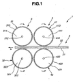
Fig. 1 is a side elevation representing a first embodiment of the electronic paper printer of the present invention. - An
electronic paper printer 1 indicated inFig. 1 is an apparatus for describing (printing) prescribed display patterns displays such as text characters, numbers, and graphics pictures onelectronic paper 2 that will be described subsequently. - This
electronic paper printer 1 has a describing head (first head) 3 for describing display patterns on theelectronic paper 2, an erasing head (second head) 4 for erasing display patterns that have been described on theelectronic paper 2, a drive mechanism (not shown) for driving the describinghead 3 and erasinghead 4 so that they revolve, and a conveyor mechanism (not shown) for conveying theelectronic paper 2. The direction of arrow A inFig. 1 is the direction theelectronic paper 2 is conveyed in. -
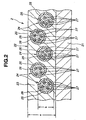
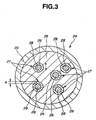
Fig. 2 is a cross-sectional diagram of an example configuration for theelectronic paper 2.Fig. 3 is a cross-sectional diagram of a micro-capsule in the electronic paper diagrammed inFig. 2 . - The
electronic paper 2 diagrammed inFig. 2 constitutes display means (display media) capable of rewriting and erasing display patterns using electrophoresis. - This
electronic paper 2 comprises paper (a sheet-form base layer exhibiting flexibility) 21 and anelectronic ink layer 22 formed on thepaper 21. The surface on the upper side of thiselectronic ink layer 22, as diagrammed inFig. 2 , is adisplay surface 20 whereon display patterns are displayed. - The
electronic ink layer 22 comprises atransparent binder 23 exhibiting light transmissivity and a plurality of micro-capsules 24 which are fixed in a state wherein they are uniformly dispersed in thebinder 23. - It is desirable that the thickness a of the
electronic ink layer 22 be from 1.5 to 2 times the outer diameter (i.e. diameter) b of the micro-capsules 24. - Polyvinyl alcohol or the like can be used as the
binder 23. - As diagrammed in
Fig. 3 , each micro-capsule 24 has amain capsule body 25 that is shaped as a hollow sphere and exhibits light transmissivity. The interior of thismain capsule body 25 is filled with aliquid solvent 26. In thisliquid 26 is dispersed a plurality ofcharged particles 27 having negative charges. - Each
charged particle 27 comprises anucleus 28 and a coveringlayer 29 that covers thenucleus 28. - The colors of the
charged particles 27 and theliquid 26 are set so as to be mutually different. If the color of thecharged particles 27 is made white, for example, the color of theliquid 26 might be made blue, red, green, or black. - When an external electric field (i.e. electric field) is applied to the micro-capsule 24, the
charged particles 27 move, inside themain capsule body 25, in a direction opposite the direction of the electric field. - If, for example, a positively charged electrode is positioned above the micro-capsule 24 (
display surface 20 side), as diagrammed inFig. 3 , an electric field is produced that is directed toward the bottom inFig. 3 , as a consequence whereof thecharged particles 27 move (float up) to the upper side, as diagrammed inFig. 3 , inside themain capsule body 25. Due to thesecharged particles 27, the color of the upper side of the micro-capsule 24, as diagrammed inFig. 3 , will turn white. - Conversely, if a negatively charged electrode is positioned on the upper side of the micro-capsule 24, as diagrammed in
Fig. 3 , an electric field will be produced that is directed toward the upper side, inFig. 3 . As a consequence, thecharged particles 27 will move down (sink) toward the lower side in themain capsule body 25, as diagrammed inFig. 3 . In this case, the liquid 26 is positioned on the upper side in themain capsule body 25, as diagrammed inFig. 3 , wherefore, if the color of the liquid is blue, the color of the upper side of the micro-capsule 24, as diagrammed inFig. 3 , will become blue. - The micro-capsules 24 are configured such that the specific gravity of the liquid 26 and the specific gravity of the charged
particles 27 become equal. - Thus, the charged
particles 27, after moving either up or down, as diagrammed inFig. 3 , can remain in a certain position for a long period of time, even if the electric field disappears, the color on the upper side of the micro-capsule 24, as diagrammed inFig. 3 , can be maintained white, and the color of the liquid can be maintained blue, for example, for a long time. In other words, the display on theelectronic paper 2 can be maintained for a long period of time. - In order to make the specific gravity of the liquid 26 and the specific gravity of the charged
particles 27 equal, furthermore, the thickness d of thecovering layer 29, for example, may be adjusted. - The outer diameter b of the micro-capsule 24 should be 180 µm or less, with 10 to 20 µm or so being preferable.
- TiO2 (rutile structure) or the like, for example, can be used for the
nuclei 28 of the chargedparticles 27. - A polyethylene or the like, for example, can be used for the
covering layer 29 of the chargedparticles 27. - For the liquid 26, a solution can be used wherein an anthraquinone-based dye is dissolved in ethylene tetrachloride and isoparaffin, for example.
- As diagrammed in
Fig. 1 , the describinghead 3 is configured by a pair ofdrums drum 31 and the outer diameter of thedrum 32 are set so as to be identical. - The outer diameter of the
drums - By making the outer diameters of the
drums drums electronic paper 2 can be increased, thereby enhancing the display pattern describing speed. - These
drums axes 312 and 322), respectively, which are mutually parallel, and thedrums drums drum 31 is on the upper side, as diagrammed inFig. 1 , that is, on theelectronic ink layer 22 side of theelectronic paper 2, and so that thedrum 32 is on the lower side, as diagrammed inFig. 1 , that is, on thepaper 21 side of theelectronic paper 2. - The interval between the outer circumferential surface of the
drum 31 and the outer circumferential surface of thedrum 32 is set so that theelectronic paper 2 can pass between thedrum 31 and thedrum 32, and so that thedrum 31 and thedrum 32 can apply pressure and electric fields on theelectronic paper 2 as sufficient and as necessary. - The
drum 31 has acylindrical drum body 311. On the outer circumferential surface of thisdrum body 311 is deployed acircuit board 313 comprising a plurality of pixel electrodes (upper electrodes). Thiscircuit board 313 will be described in detail subsequently. - The
drum 32, meanwhile, has acylindrical drum body 321. On the outer circumferential surface of thisdrum body 321 is deployed a common electrode (lower electrode) 323. -
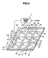
Fig. 4 is a diagram (block diagram) which represents in model form the condition wherein thecircuit board 313 is deployed. The direction of arrow A inFig. 4 is the direction in which theelectronic paper 2 is conveyed. -
Fig. 5 is a side elevation representing one pixel in the describinghead 3. The direction of arrow A inFig. 5 is the direction in which theelectronic paper 2 is conveyed. - As diagrammed in
Fig. 4 , thecircuit board 313 has asubstrate 61 formed of a resin exhibiting flexibility (elasticity). - On this
substrate 61 are formed, respectively, a plurality ofsquare pixel electrodes 64 deployed (arrayed) in a matrix arrangement, a plurality of thin film transistors (TFTs) (switching elements) 65 for switching thepixel electrodes 64 between conducting and non-conducting states, respectively, agate driver 62 for applying voltages (signals) to the gates of thethin film transistors 65, asource driver 63 for applying voltages (signals) to the sources of thethin film transistors 65, a plurality ofgate lines 621 that extend laterally, as diagrammed inFig. 4 , and a plurality ofsource lines 631 that extend vertically, as diagrammed inFig. 4 . - Each
pixel electrode 64 corresponds to one pixel (bit). - There is no particular limitation on the pitch of the
pixel electrodes 64, but a pitch of 500 to 5000 dpi (dots per inch) or so is desirable. - In the present invention, needless to say, the shape of the
pixel electrodes 64 is not limited to a square shape. - In the present invention, furthermore, the pattern in which the
pixel electrodes 64 are arrayed is not limited to a matrix arrangement. There is no reason why thepixel electrodes 64 may not be deployed in a delta arrangement, for example. - Hereinafter, with respect to
Fig. 4 , the uppermost laterally oriented array is called the "first row" and the Nth laterally oriented array from the top is called the "Nth row." - With respect to
Fig. 4 , furthermore, the leftmost vertically oriented array is called the "first column" and the Nth vertically oriented array from the left side is called the "Nth column." - To the
gate drive 62 is connected each of the plurality ofgate lines 621 that extend laterally, as diagrammed inFig. 4 . - To the
source driver 63, furthermore, is connected each of the plurality ofsource lines 631 that extend vertically, as diagrammed inFig. 4 . - Each of the
thin film transistors 65, moreover, is connected to acorresponding gate line 621. - Each of the sources of the
thin film transistors 65, furthermore, is connected to acorresponding source line 631, and each of the drains of thethin film transistors 65 is connected to acorresponding pixel electrode 64. - The
gate driver 62 sequentially scans thegate lines 621 one row (line) at a time. - "To scan the Nth
row gate line 621," for example, means to apply a voltage (scan voltage) precisely during a scanning time (time) t to the gates of all of thethin film transistors 65 in the Nth row, and [thus] turn on all of the thin film transistors 65 (i.e. the gates of the thin film transistors 65) in the Nth row for precisely the scanning time t. - Thus the role of the
gate driver 62 is to sequentially scan the Nth row, and then the N+1'th row, and then the N+2'th row, that is, to sequentially turn on all of thethin film transistors 65 in each of the rows, in row units (i.e. one row at a time), for precisely the scanning time t. - The
source driver 63 is also called a data line drive circuit. This is a circuit that applies a voltage corresponding to printing information (information indicating a display pattern) to thepixel electrodes 64 via the source lines 631 and thethin film transistors 65 when a scanning voltage is applied to aprescribed gate line 621, that is, when all of thethin film transistors 65 in a prescribed row are turned on. - When a scanning voltage is applied to a
prescribed gate line 621, the voltage noted above is applied to theprescribed source line 631, so that the correspondingpixel electrode 64 conducts. Thus a negative voltage at a prescribed level can be applied to thecorresponding pixel electrode 64, for example, and, as diagrammed inFig. 5 , thatpixel electrode 64 can be given a negative charge, for example. When this is done, if the potential on thecommon electrode 323 has been set at 0 volts, an electric field will be formed (will appear) that is directed toward thatpixel electrode 64. - The level of the voltage applied between the
pixel electrode 64 noted above and the common electrode 323 (that is, the potential difference between thatpixel electrode 64 and the common electrode 323) is not particularly limited, but, in terms of absolute values, a voltage of 10 volts or higher is desirable, and 20 volts or higher is even more preferable. - The drives for the
thin film transistors 65 noted earlier are controlled, respectively, by control means 7 via thegate driver 62 and thesource driver 63. - The control means 7 are ordinarily configured by an integrated circuit comprising a logic circuit and a memory circuit. The control means 7 control, in addition to the
thin film transistors 65, thethin film transistors 65, etc., on thedrum 41 of the erasing head 4 (described subsequently), and also the entireelectronic paper printer 1. - It is desirable that the formation of the
circuit board 313 on the outer circumferential surface of thedrum body 311, as described earlier, be performed as described below, for example. - First, a circuit unit comprising a thin film transistor array and pixel electrode array, etc., as described in the foregoing, is formed on a prescribed substrate (not shown), and this is then peeled away from the substrate by a prescribed method and transferred to the
substrate 61. Thus is obtained thecircuit board 313. For the details of this method, the Japanese Patent Kokai No.H10-125930/1998 - Next, this
circuit board 313 is wrapped about and fixed to the outer circumferential surface of thedrum body 311. - As diagrammed in
Fig. 1 , the erasinghead 4 is deployed on the right side (inFig. 1 ) of the describing head 3 (i.e. on the upstream side thereof as respecting the direction of conveyance of the electronic paper 2), separated from the describinghead 3 by a prescribed distance. - This erasing
head 4, similarly to the describinghead 3 described earlier, is configured by a pair ofdrums drum 41 and thedrum 42 are set equal to the outer diameters of thedrum 31 and drum 32 of the describinghead 3 described earlier (the outer diameter of thedrum 41 and the outer diameter of thedrum 42 also being set equal). - There is no particular limitation on the outer diameter of the
drums drums - By making the outer diameters of the
drums drums electronic paper 2 can be increased, thereby enhancing the display pattern erasing speed. Thesedrums axes 412 and 422), respectively, which are mutually parallel, and thedrums head 3 described earlier. Thesedrums head 3 described earlier, so that thedrum 41 is on the upper side, as diagrammed inFig. 1 , that is, on theelectronic ink layer 22 side of theelectronic paper 2, and so that thedrum 42 is on the lower side, as diagrammed inFig. 1 , that is, on thepaper 21 side of theelectronic paper 2. - The
drum 41 has acylindrical drum body 411. On the outer circumferential surface of thisdrum body 411 is deployed acircuit board 413 comprising a plurality of pixel electrodes (upper electrodes) 64, as in the describinghead 3 described earlier. Thiscircuit board 413 is like thecircuit board 313 in the describinghead 3 described earlier, wherefore the description thereof will be abridged. - The
drum 42, meanwhile, has acylindrical drum body 421. On the outer circumferential surface of thisdrum body 421 is deployed a common electrode (lower electrode) 423. -
Fig. 6 is a side elevation of one pixel in the erasinghead 4. The direction of arrow A inFig. 6 is the direction in which theelectronic paper 2 is conveyed. - The
gate driver 62 sequentially scans thegate lines 621 one row (line) at a time (cf.Fig. 4 ). - "To scan the Nth
row gate line 621," for example, means to apply a voltage (scan voltage) precisely during a scanning time (time) t to the gates of all of thethin film transistors 65 in the Nth row, and [thus] turn on all of the thin film transistors 65 (i.e. the gates of the thin film transistors 65) in the Nth row for precisely the scanning time t. - Thus the role of the
gate driver 62 is to sequentially scan the Nth row, and then the N+1'th row, and then the N+2'th row, that is, to sequentially turn on all of thethin film transistors 65 in each of the rows, in row units (i.e. one row at a time), for precisely the scanning time t. - The
source driver 63 is also called a data line drive circuit. This is a circuit that applies a voltage to thepixel electrodes 64 via the source lines 631 and thethin film transistors 65 when a scanning voltage is applied to aprescribed gate line 621, that is, when all of the thin film transistors in a prescribed row are turned on. - When a scanning voltage is applied to a
prescribed gate line 621, the voltage noted above is applied to theprescribed source line 631, so that the correspondingpixel electrode 64 conducts. Thus a positive voltage at a prescribed level can be applied to thecorresponding pixel electrode 64, and, as diagrammed inFig. 6 , thatpixel electrode 64 can be given a positive charge. When this is done, an electric field will be formed that is directed away from thatpixel electrode 64 toward thecommon electrode 423. - The level of the voltage applied between the
pixel electrode 64 noted above and the common electrode 423 (that is, the potential difference between thatpixel electrode 64 and the common electrode 423) is not particularly limited, but, in terms of absolute values, a voltage of 10 volts or higher is desirable, and 20 volts or higher is even more preferable. - The formation of the
circuit board 413 on the outer circumferential surface of thedrum body 411 described in the foregoing should be performed using the same method as for forming thecircuit board 313 to the outer circumferential surface of thedrum body 311 as described earlier. - The action of the
electronic paper printer 1 is described next. - When describing display patterns on the
electronic paper 2 with theelectronic paper printer 1, as diagrammed inFig. 1 , thedrum 31 of the describinghead 3 turns clockwise, as shown inFig. 1 , a prescribed number of revolutions (turning speed), while thedrum 32 turns counterclockwise, as shown inFig. 1 , the same number of revolutions as thedrum 31. This turning is performed by a drive mechanism. - Similarly, the
drum 41 of the erasinghead 4 turns clockwise, as shown inFig. 1 , the same number of revolutions as thedrum 31, while thedrum 42 turns counterclockwise, as shown inFig. 1 , the same number of revolutions as thedrum 41. This turning is likewise performed by a drive mechanism. - Furthermore, since the outer diameters of the
drums drums - The
electronic paper 2 is conveyed by the conveyor mechanism from the left side, as shown inFig. 1 , to the erasinghead 4. - The control means 7 drive the
gate driver 62, scan all of thethin film transistors 65 in the erasinghead 4, and turn them on, one row at a time. - When this is done, the control means 7 also drives the
source driver 63, and outputs the same electrical potential to all of the source lines 631. - The control means 7, moreover, begin the scanning and the signal output described above before the
electronic paper 2 contacts thepixel electrodes 64 in each column. - Thus, as diagrammed in
Fig. 6 , a positive voltage, for example, at a prescribed level, is applied to all of thepixel electrodes 64. And, if the potential on thecommon electrode 423 has been set at 0 volts, electric fields are formed from the correspondingpixel electrodes 64 toward thecommon electrode 423. - The
electronic paper 2 is held between thedrum 41 and thedrum 42 and carried along in the direction of arrow A. That is, theelectronic paper 2, from the leading end (the part on the left inFig. 1 ), passes successively between thedrums 41 and thedrum 42. When this happens, theelectronic paper 2 is subjected to prescribed pressures and placed in the electric fields described earlier (i.e. subjected to those electric fields), sequentially from the leading end, by thedrum 41 and thedrum 42. - As one example, a description is now given of a mode wherewith, after the entire surface of the
electronic paper 2 is made white by the erasinghead 4, blue text characters and graphics are drawn by the describinghead 3. - As diagrammed in
Fig. 7 , the chargedparticles 27 in theelectronic paper 2 placed in the electric field as noted above move to the upper side, as shown inFig. 7 , in themain capsule units 25, respectively, due to that electric field. These chargedparticles 27 cause thedisplay surface 20 of theelectronic paper 2 corresponding thereto to turn white. - Thereafter, in the same manner, the
electronic paper 2 passes between thedrum 41 and thedrum 42, whereupon the color of thedisplay surface 20 thereof becomes white. - Then, when the
electronic paper 2 passes between thedrum 41 and thedrum 42 all the way to the basal end thereof (the part on the right side inFig. 1 ), the color of thedisplay surface 20 of theelectronic paper 2 will be completely white. That is, all of the display patterns described on theelectronic paper 2 will be erased (i.e. theelectronic paper 2 will be reset). - Furthermore, as diagrammed in
Fig. 1 , theelectronic paper 2 is carried along by thedrum 41 and thedrum 42 in the direction of arrow A and thereby conveyed to the describinghead 3. - The control means 7, while controlling the gate voltage on the
thin film transistors 65, also control the source voltages on thethin film transistors 65 based on signals indicating display patterns (such as image signals, for example). - More specifically, the control means 7 drive the
gate driver 62 and scan the gate lines 621 on a time-division basis. As diagrammed inFig. 4 , first of all, a pulse voltage is applied to the firstrow gate line 621 for the time t, thus turning on (opening) the gates of all of thethin film transistors 65 in the first row. That is, all of thethin film transistors 65 in the first row are turned on for precisely the time t. Next, a pulse voltage is applied to the secondrow gate line 621, thus turning on all of thethin film transistors 65 in the second row for precisely the time t. Thereafter, pulse voltages are applied sequentially to the [remaining]gate lines 621 in the same manner. - Then the control means 7 send signals (image signals, for example) corresponding to the target row or rows to the
source driver 63, drive thesource driver 63, and, during the time t that thethin film transistors 65 in the target row or rows are turned on, applies a voltage for each row in the targeted rows to the sources of thethin film transistors 65 corresponding to the target row or rows. Thus voltages corresponding to the signals noted above are applied across the sources and drains in thethin film transistors 65 of the target row or rows. If the target row is the second row, for example, when -20 volts are applied to the sources of thethin film transistors 65 in the second column, it is only necessary that the voltage on the second column of the source driver, that is, on the secondcolumn source line 631, be -20 volts. - Thus, as diagrammed in
Fig. 5 , a negative voltage at a prescribed level is applied to thetarget pixel electrodes 64, and thetarget pixel electrodes 64 are charged negatively. If the potential on thecommon electrode 323 has been set at 0 volts, moreover, electric fields will be formed that respectively are oriented toward thetarget pixel electrodes 64 opposing thatcommon electrode 323. - As diagrammed in
Fig. 1 , theelectronic paper 2 is held between thedrum 31 and thedrum 32 and carried along in the direction of arrow A. That is, theelectronic paper 2, from the leading end, passes successively between thedrums 31 and thedrum 32. When this happens, theelectronic paper 2 is subjected to prescribed pressures and placed in the electric fields described earlier, sequentially from the leading end, by thedrum 31 and thedrum 32. - As diagrammed in
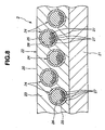
Fig. 8 , the chargedparticles 27 in theelectronic paper 2 placed in the electric field as noted above move to the lower side, as shown inFig. 8 , in themain capsule units 25, respectively, due to that electric field. In this case, the liquid 26 is positioned on the upper side, as shown inFig. 8 , inside themain capsule units 25, wherefore the color of thedisplay surface 20 of theelectronic paper 2 corresponding thereto turns blue. That is, a portion of the display pattern is described on theelectronic paper 2. - Thereafter, in the same manner, when the
electronic paper 2 passes between thedrum 31 and thedrum 32, a portion of the display pattern is described. - Then, when the
electronic paper 2 has passed through thedrum 31 and thedrum 32 up to the basal end thereof, all of the display pattern will have been described on theelectronic paper 2. Thereupon, the describing of the display pattern on theelectronic paper 2 is completed. - When the display pattern on this
electronic paper 2 is rewritten, or when a display pattern is described on anotherelectronic paper 2, as described in the foregoing, first the display pattern is erased by the erasinghead 4, and then the new display pattern is described. - When erasing a display pattern from the
electronic paper 2, only erasure of the display pattern by the erasinghead 4 described in the foregoing is performed. - As described in the foregoing, if this
electronic paper printer 1 is employed, it is possible to repeatedly describe such prescribed display patterns as text characters, numbers, and graphics, etc., on theelectronic paper 2. - Because the display patterns are described on the
electronic paper 2, moreover, the display patterns are easy to view, as compared to when display patterns are displayed on a display [screen], but no waste of paper (natural resources) is involved as when printing the display patterns on paper for viewing. - Also, with this
electronic paper printer 1, because the describing is done by the drum-shaped describing head 3 (that is, because both thepixel electrodes 64 and thecommon electrode 423, respectively, in the describinghead 3 are formed with curved surfaces), when describing is being performed, pressure can be applied uniformly to theelectronic paper 2, wherefore the display patterns can be described properly and definitely on theelectronic paper 2. - Similarly, because erasing is done by the drum-shaped erasing head 4 (that is, because both the
pixel electrodes 64 and thecommon electrode 423, respectively, in the erasinghead 4 are formed with curved surfaces), when erasing is being performed, pressure can be applied uniformly to theelectronic paper 2, wherefore it is possible to erase display patterns described on theelectronic paper 2 definitely and uniformly. - With this
electronic paper 1, furthermore, the shapes of the drums in the erasinghead 4 and describinghead 3 are made cylindrical, wherefore it is possible to perform erasing and description of display patterns continuously without being limited by the length of theelectronic paper 2 in the lateral direction as shown inFig. 1 . - With the present invention, the erasing
head 4 in theelectronic paper printer 1 may also be configured so that it can form a comprehensive erasing electric field. This will be shown in conjunction with a second embodiment. -
Fig. 9 is a side elevation of an erasing head in a second embodiment of the electronic paper printer of the present invention. - The configuration of the
electronic paper printer 1 in this second embodiment is the same as that of theelectronic paper printer 1 in the first embodiment, excepting in that the structure of an erasinghead 5 differs from that of the erasinghead 4 in theelectronic paper printer 1 in the first embodiment, described earlier. In other words, in theelectronic paper printer 1 in this second embodiment, the erasinghead 4 diagrammed inFig. 1 is replaced by the erasinghead 5 diagrammed inFig. 9 . - Accordingly, the erasing
head 5 diagrammed inFig. 9 is deployed on the right side of the describinghead 3, as diagrammed inFig. 1 , separated from the describinghead 3 by a prescribed distance. - This erasing
head 5, as the describinghead 3 and erasinghead 4 described earlier, is configured by a pair of drums, namely thedrums drum 51 and thedrum 52 are set so as to be equal to the outer diameters of thedrum 31 and thedrum 32 of the describinghead 3, described earlier (the external diameter of thedrum 51 being set equal to the external diameter of the drum 52). - There is no particular limitation on the external diameters of the
drums drums - By making the outer diameters of the
drums drums electronic paper 2 can be increased, thereby enhancing the display pattern erasing speed. - These
drums axes 512 and 522), respectively, which are mutually parallel, and thedrums head 3 and the erasinghead 4 described earlier. Thesedrums head 4 described earlier, so that thedrum 51 is on the upper side, as diagrammed inFig. 9 , that is, on theelectronic ink layer 22 side of theelectronic paper 2, and so that thedrum 52 is on the lower side, as diagrammed inFig. 9 , that is, on thepaper 21 side of theelectronic paper 2. - The
drum 51 has acylindrical drum body 511. On the outer circumferential surface of thisdrum body 511 is deployed a singleupper electrode 513. - The
drum 52, meanwhile, has acylindrical drum body 521. On the outer circumferential surface of thisdrum body 521 is deployed a singlelower electrode 523. - The
upper electrode 513 and thelower electrode 523 are formed, for example, of a metal thin film or an electrically conducting ceramic thin film or the like. - The
driver 6 is driven by commands from the control means 7, and voltages are applied across thisupper electrode 513 andlower electrode 523. If, for example, a positive voltage (plus potential) is applied to theupper electrode 513 and a negative voltage (minus potential) is applied to thelower electrode 523, an electric field will be formed, directed away from theupper electrode 513 and toward thelower electrode 523, where theupper electrode 513 and thelower electrode 523 are in opposition. - There is no particular limitation on the level of the voltage applied across these electrodes, but, in terms of absolute values, 10 volts or higher is desirable, and 20 volts or higher is even more preferable.
- The action of the erasing
head 5 in theelectronic paper printer 1 of the second embodiment is described next. - The action of the
electronic paper printer 1 is the same as that of theelectronic paper printer 1 in the first embodiment, described earlier, with the exception of the action of the erasinghead 5. Hence only the action of the erasinghead 5 is described below. - The
drum 51 of the erasinghead 5 is turned clockwise, as shown inFig. 9 , by the drive mechanism, the same number of revolutions as thedrum 31, while thedrum 52 is thereby turned counterclockwise, as shown inFig. 9 , the same number of revolutions as thedrum 51. - In the second embodiment, furthermore, the outer diameters of the
drums drums - The
electronic paper 2 is conveyed by the conveyor mechanism from the right side, as shown inFig. 9 , to the erasinghead 5, as indicated by arrow A. - The control means 7, before the
electronic paper 2 is wound in between thedrums driver 6, and apply a voltage across theupper electrode 513 and thelower electrode 523. If, for example, as diagrammed inFig. 9 , a positive voltage is applied to theupper electrode 513 and a negative voltage is applied to thelower electrode 523, an electric field will be formed that is directed from theupper electrode 513 toward thelower electrode 523 at the place where theelectronic paper 2 is held between thedrums upper electrode 513 and thelower electrode 523 are in opposition. - The
electronic paper 2 passes successively between thedrum 51 and thedrum 52 from the leading end (the part on the left inFig. 9 ). When this happens, as described in conjunction with the first embodiment, the prescribed pressures and electric fields are applied sequentially, from the leading end. - In this manner, when the
electronic paper 2 has been placed in the electric field described in the foregoing from the leading end to the basal end, thedisplay surface 20 of theelectronic paper 2 becomes completely white. That is, even if display patterns have been described on theelectronic paper 2, they are entirely erased by this erasing head 5 (the electronic paper is reset). - As described in the foregoing, when this erasing
head 5 is employed, the structure can be fabricated simply and easily, control is simple, and theupper electrode 513 and thelower electrode 523, respectively, are formed singly on thedrums electronic paper 2. - With the present invention, moreover, the erasing
heads - A third embodiment of the electronic paper printer of the present invention is described next.
-
Fig. 10 is a side elevation representing the third embodiment of the electronic paper printer of the present invention. Points in common with theelectronic paper printer 1 of the first embodiment, described earlier, are not further described here. The main points of difference are described. - As diagrammed in
Fig. 10 , theelectronic paper printer 1 has a describinghead 8 for erasing display patterns described on theelectronic paper 2 and describing display patterns thereon (capable also of overwriting), a drive mechanism (not shown) for driving the describinghead 8 so that it turns, and a conveyor mechanism (not shown) for conveying theelectronic paper 2. The direction of arrow A inFig. 10 is the direction in which theelectronic paper 2 is conveyed. - The describing
head 8 is configured by a pair of drums, 81 and 82, supported so that they freely turn. The outer diameter of thedrum 81 and the outer diameter of thedrum 82 are set equal. - There is no particular limitation on the outer diameters of the
drums - These
drums axes 812 and 822), respectively, which are mutually parallel, and thedrums drums drum 81 is on the upper side, as diagrammed inFig. 10 , that is, on theelectronic ink layer 22 side of theelectronic paper 2, and so that thedrum 82 is on the lower side, as diagrammed inFig. 10 , that is, on thepaper 21 side of theelectronic paper 2. - The
drum 81 has acylindrical drum body 811. On the outer circumferential surface of thisdrum body 811 is deployed acircuit board 813 comprising a plurality of pixel electrodes (upper electrodes). - The
drum 82, meanwhile, has acylindrical drum body 821. On the outer circumferential surface of thisdrum body 821 is deployed acircuit board 823 comprising a plurality of pixel electrodes (lower electrodes). - The
circuit boards circuit board 313 in the describinghead 3 of theelectronic paper printer 1 in the first embodiment described earlier, moreover, and so are not further described here. -
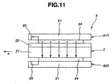
Fig. 11 andFig. 12 , respectively, are side elevations representing one pixel in the describinghead 8. The direction of arrow A inFig. 11 andFig. 12 is the direction in which theelectronic paper 2 is conveyed. - With this
electronic paper printer 1, as diagrammed inFig. 11 and12 , the configuration is made so that positioning is done by a timing belt or encoder or the like, for example, so that the positions of thepixel electrodes 64 in thedrum 81 coincide with the positions of thepixel electrodes 64 in thedrum 82 corresponding thereto. - When, in the
thin film transistors 65, the respective gates are turned on (i.e. a voltage is applied thereto), and a voltage at a prescribed level is applied to the sources thereof, the correspondingpixel electrodes 64 thereby conduct. - As diagrammed in
Fig. 11 , when the gates ofthin film transistors 65 in thedrum 81 are turned on and a voltage is applied to the sources thereof, a positive voltage at a prescribed level is applied to thecorresponding pixel electrodes 64, and thosepixel electrodes 64 are positively charged. When that happens, the gates of thethin film transistors 65 in thedrum 82 are turned on, with the same timing wherewith the gates of the thin film transistors in thedrum 81 are turned on, either a zero (0 volt) voltage or negative voltage is applied to the sources thereof, and thosepixel electrodes 64 are either zero-charged (charge quantity = 0) or negatively charged. Thus electric fields are formed that are directed from thepixel electrodes 64 in thedrum 81 to thepixel electrodes 64 in thedrum 82. - Conversely, as diagrammed in
Fig. 12 , when the gates ofthin film transistors 65 in thedrum 82 are turned on and a voltage is applied to the sources thereof, a positive voltage at a prescribed level is applied to thecorresponding pixel electrodes 64, and thosepixel electrodes 64 are positively charged. When that happens, the gates of thethin film transistors 65 in thedrum 81 are turned on, with the same timing wherewith the gates of the thin film transistors in thedrum 82 are turned on, either a zero voltage or negative voltage is applied to the sources thereof, and thosepixel electrodes 64 are either zero-charged or negatively charged. Thus electric fields are formed that are directed from thepixel electrodes 64 in thedrum 82 to thepixel electrodes 64 in thedrum 81. - There is no particular limitation on the level of the voltage applied across the
pixel electrodes 64 in thedrum 81 and thepixel electrodes 64 in thedrum 82, but 10 volts or greater is desirable, and 20 volts or greater is even more preferable. - The formation of the
circuit board 813 on the outer circumferential surface of thedrum body 811 noted above and the formation of thecircuit board 823 on the outer circumferential surface of thedrum body 821 noted above, respectively, should be performed with the same method used for forming thecircuit board 313 on the outer circumferential surface of thedrum body 311 in theelectronic paper printer 1 in the first embodiment described earlier. - Next, the action of the
electronic paper printer 1 in the third embodiment is briefly described. - With this
electronic paper printer 1, when a display pattern is described on theelectronic paper 2, the control means 7, based on signals indicating the display pattern (such as image signals, for example), turn on prescribedthin film transistors 65 in thedrums gate driver 62 and thesource driver 63 for thedrums - That is, when the color of prescribed portions (pixels) on the
display surface 20 of theelectronic paper 2 is to be made blue, the gates in thethin film transistors 65 in thedrum 81 and thethin film transistors 65 in thedrum 82 corresponding to the pixels to be made blue are turned on, a positive voltage is applied to the sources of thethin film transistors 65 in thedrum 82, and a zero or negative voltage is applied to the sources of thethin film transistors 65 in thedrum 81. - Thus, as diagrammed in
Fig. 12 , a positive voltage of a prescribed level is applied to thetarget pixel electrodes 64 in thedrum 82, and thosepixel electrodes 64 are positively charged. Also, a zero voltage or a negative voltage at a prescribed level is applied to the targetedpixel electrodes 64 in thedrum 81, and thosepixel electrodes 64 are given a zero or negative charge. Thereupon, electric fields are formed that, respectively, are directed from thetarget pixel electrodes 64 in thedrum 82 to thecorresponding pixel electrodes 64 in thedrum 81. - Conversely, when the color of prescribed portions (pixels) on the
display surface 20 of theelectronic paper 2 is to be made white, the gates in thethin film transistors 65 in thedrum 81 and thethin film transistors 65 in thedrum 82 corresponding to the pixels to be made white are turned on, a positive voltage is applied to the sources of thethin film transistors 65 in thedrum 81, and a zero or negative voltage is applied to the sources of thethin film transistors 65 in thedrum 82. - Thus, as diagrammed in
Fig. 11 , a positive voltage at a prescribed level is applied to thetarget pixel electrodes 64 in thedrum 81, and thosepixel electrodes 64 are positively charged. Also, a zero voltage or a negative voltage at a prescribed level is applied to the targetedpixel electrodes 64 in thedrum 82, and thosepixel electrodes 64 are given a zero or negative charge. Thereupon, electric fields are formed that, respectively, are directed from thetarget pixel electrodes 64 in thedrum 81 to thecorresponding pixel electrodes 64 in thedrum 82. - As diagrammed in
Fig. 8 , the chargedparticles 27 in theelectronic paper 2 placed in the electric fields directed from thepixel electrodes 64 in thedrum 82 toward thepixel electrodes 64 in thedrum 81 move, respectively, to the lower side, as shown inFig. 8 , in themain capsule bodies 25 due to those electric fields. In that case, the liquid 26 is positioned on the upper side, as shown inFig. 8 , inside themain capsule bodies 25, wherefore the color of thedisplay surface 20 of theelectronic paper 2 corresponding thereto turns blue. - Conversely, as diagrammed in
Fig. 7 , the chargedparticles 27 in theelectronic paper 2 placed in electric fields directed from thepixel electrodes 64 in thedrum 81 toward thepixel electrodes 64 in thedrum 82 move, respectively, to the upper side, as shown inFig. 7 , inside themain capsule bodies 25 due to those electric fields, and, due to those chargedparticles 27, the color of thedisplay surface 20 of theelectronic paper 2 corresponding thereto turns white. - Furthermore, in order to erase display patterns from the
electronic paper 2, and make the entire surface thereof white, all of thepixel electrodes 64 on thedrum 81 are successively given a positive charge, and, simultaneously therewith, all of thepixel electrodes 64 on thedrum 82 are successively given a zero or negative charge. Thereby, at the places where thepixel electrodes 64 on thedrum 81 and thepixel electrodes 64 on thedrum 82 are in opposition, electric fields are formed which are directed from thepixel electrodes 64 on thedrum 81 toward thepixel electrodes 64 on thedrum 82, and theentire display surface 20 of theelectronic paper 2 is made white. - Conversely, to make the
entire display surface 20 of theelectronic paper 2 blue, the electric fields are formed in a direction opposite to that described above, that is, electric fields are formed that are directed from thepixel electrodes 64 in thedrum 82 toward thepixel electrodes 64 in thedrum 81. - As described in the foregoing, by implementing this
electronic paper printer 1, prescribed display patterns can be described on theelectronic paper 2, properly, definitely, and repeatedly, as with theelectronic paper printer 1 in the first embodiment described earlier. - Moreover, with this
electronic paper printer 1, theelectronic paper 2 can be overwritten, wherefore, an erasing head is unnecessary, so that the structure can simplified. - Next, a fourth embodiment of the electronic paper printer of the present invention is described.
-
Fig. 13 is a side elevation representing the fourth embodiment of the electronic paper printer of the present invention. - The
electronic paper printer 1 in this fourth embodiment is a electronic paper printer that comprises an overwrite-capable describing head 9. The structure thereof is identical to that of theelectronic paper printer 1 in the third embodiment, excepting in that the electrode structure on thedrum 92 in the describing head 9 differs from the electrode structure on thedrum 52 of the describinghead 5 in theelectronic paper printer 1 in the third embodiment. Accordingly, no further description is given here of the points in common with theelectronic paper printer 1 in the third embodiment, but the main points of difference are described. - As diagrammed in
Fig. 13 , in the describing head 9 of theelectronic paper printer 1 in this fourth embodiment, the drum 91 [components], that is, adrum body 911, a turningshaft 912 andcircuit board 913, adrum body 921, and a turningshaft 922, respectively, are the same as those [corresponding components] in the third embodiment. - More specifically, the
circuit board 913, comprising a plurality of pixel electrodes (upper electrodes), is deployed on the outer circumferential surface of thedrum body 911 of thedrum 91. - On the outer circumferential surface of the
drum body 921 of thedrum 92, however, a common electrode (lower electrode) 923 is deployed. - Accordingly, in terms of one pixel in the describing head 9, the side elevation representing the action when an electric field is formed between a pixel electrode and the
common electrode 923, and a display pattern on theelectronic paper 2 is overwritten, is as given in eitherFig. 5 orFig. 6 . - Next, the action of the
electronic paper printer 1 in the fourth embodiment is briefly described. - With this
electronic paper printer 1, when describing a display pattern on theelectronic paper 2, the control means 7, based on signals indicating the display pattern (such as image signals, for example), turn on prescribedthin film transistors 65 on thedrum 91, via thegate driver 62 and thesource driver 63 for thedrum 91, apply a prescribed voltage (potential) to the sources thereof, and hold (set) the voltage (potential) on thecommon electrode 923 of thedrum 92 to a prescribed value. Thereby, two electric fields are selectively formed, having differing directions, between thepixel electrodes 64 and thecommon electrode 923, and the display pattern is overwritten. - There are two methods, for example, as described next, for performing overwriting with the
electronic paper printer 1 wherein thecircuit board 913 is deployed only on one of the drums, namely thedrum 91, as diagrammed inFig. 13 .Overwriting methods -
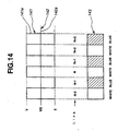
Fig. 14 is a diagram (theory diagram for method 1) which represents the voltages (potentials) on thepixel electrodes 64 in thedrum 91 and thecommon electrode 923 in thedrum 92, together with a display pattern corresponding thereto. Method 1 (i.e. the action of the electronic paper printer 1) is now described with reference toFig. 14 . - With this method, to effect overwriting on the
electronic paper 2, thevoltage 142 on thecommon electrode 923 is set to a value intermediate between the maximum and minimum values of thevoltage 141 on the pixel electrodes 64 (intermediate value = constant value). More specifically, in the case where thevoltage 141 on thepixel electrodes 64 varies from 0 to V volts (case where maximum value = V volts and minimum value = 0 volts), thevoltage 142 on thecommon electrode 142 is set at V/2 volts. - An example is now described.
- When the
display pattern 143 diagrammed inFig. 14 , for example, is to be described in a specific row on theelectronic paper 2, and the gates of thethin film transistors 65 in the row corresponding to that row are turned on, the voltages indicated by thevoltage pattern 141a are applied to the sources of thosethin film transistors 65, that is, voltages of either 0 or V volts are applied. When that is done, thevoltage 142 on thecommon electrode 923 is set to the voltage indicated by thevoltage pattern 142a, that is, to V/2 volts. - When this is done, in the (N-2) column, for example, the
voltage 141 on thepixel electrodes 64 is V volts and thevoltage 142 on thecommon electrode 923 is V/2 volts. Therefore, electric fields are formed which are directed from thepixel electrodes 64 to thecommon electrode 923, and the chargedparticles 27 in theelectronic paper 2 move, respectively, to the upper side, as shown inFig. 13 , inside themain capsule bodies 25, whereupon the color of thedisplay surface 20 of theelectronic paper 2 is made white. - Conversely, at the (N-1) column, the
voltage 141 on thepixel electrodes 64 is 0 volts and the voltage on thecommon electrode 923 is V/2 volts, wherefore electric fields are formed that are directed from thecommon electrode 923 toward thepixel electrodes 64, and the chargedparticles 27 in theelectronic paper 2 move, respectively, to the lower side, as shown inFig. 13 , inside themain capsule bodies 25, whereupon the color of thedisplay surface 20 of theelectronic paper 2 turns blue. - Thereafter, in like manner, the direction of the electric fields formed between the
pixel electrodes 64 and thecommon electrode 923, which is to say the color of theelectronic paper 2, will be determined according to thevoltages 141 on thepixel electrodes 64 for the Nth column to the (N+3) column, and thedisplay pattern 143 can be described in the prescribed rows on theelectronic paper 2. - In this manner, the colors in prescribed locations (pixels) on the
display surface 20 of theelectronic paper 2 are determined solely by thevoltages 141 on thepixel electrodes 64, on a one-to-one basis. Therefore, irrespective of what color thedisplay surface 20 of theelectronic paper 2 was before (prior to description), display patterns can be described on thatelectronic paper 2 merely with a single passage of theelectronic paper 2 between thedrum 91 and thedrum 92 in the describing head 9 (i.e. a white and blue pattern is determined on a one-to-one basis). In other words, display patterns on theelectronic paper 2 can be overwritten. -
Fig. 15 is a diagram (theory diagram for method 2) which represents the voltages (potentials) on thepixel electrodes 64 in thedrum 91 and thecommon electrode 923 in thedrum 92, together with a display pattern corresponding thereto. Method 2 (i.e. the action of the electronic paper printer 1) is now described with reference toFig. 15 . - With this method, to effect overwriting on the
electronic paper 2, thevoltage 152 on thecommon electrode 923 is fluctuated between the maximum value of thevoltage 151 on the pixel electrodes 64 (V volts inFig. 15 ) and the minimum value thereof (0 volts inFig. 15 ) (common potential oscillation). That is, when a one-row description is to be made in a desired row on theelectronic paper 2, during the time that the gates of thethin film transistors 65 in the row corresponding to that row are turned on, thevoltage 152 on thecommon electrode 923 is switched, either from V volts to 0 volts, or from 0 volts to V volts (setting to V volts and 0 volts on a time-division basis). - Furthermore, the turning drive for the
drums drums - An example is now described.
- When the
display pattern 153 diagrammed inFig. 15 , for example, is to be described in a specific row on theelectronic paper 2, and the gates of thethin film transistors 65 in the row corresponding to that row are turned on, the voltages indicated by thevoltage pattern 151a are applied to the sources of thosethin film transistors 65, that is, voltages of either 0 or V volts are applied. When that is done, thevoltage 152 on thecommon electrode 923 is held at the voltage indicated by thevoltage pattern 152a, that is, to V volts, for a prescribed time, and then, when the gates of thethin film transistors 65 noted above continue to be turned on, [the voltage 152] is switched to the voltage indicated by thevoltage pattern 152b, that is, to 0 volts, and held for a prescribed time. - When this is done, when the
voltage 152 on thecommon electrode 64 is V volts, effective electric fields are formed, in the area indicated inFig. 15 , only between thecommon electrode 923, on the one hand, and thepixel electrodes 64 in the (N-1) column, (N+1) column, and (N+3) column, on the other. At this time, the electric fields are formed so that they are directed from thecommon electrode 923 toward thepixel electrodes 64. Therefore, the color of thedisplay surface 20 of theelectronic paper 2 is made blue in these portions. - Conversely, when the
voltage 152 on thecommon electrode 64 is 0 volts, effective electric fields are formed, in the area indicated inFig. 15 , only between thecommon electrode 923, on the one hand, and thepixel electrodes 64 in the (N-2) column, Nth column, and (N+2) column, on the other. At this time, the electric fields are formed so that they are directed from thepixel electrodes 64 toward thecommon electrode 923. Therefore, the color of thedisplay surface 20 of theelectronic paper 2 is made white in these portions. Furthermore, at this time, the voltage between thecommon electrode 923, on the one hand, and thepixel electrodes 64 in the (N-1) column, (N+1) column, and (N+3) column, on the other, is 0 volts, and no electric field is formed between these electrodes, wherefore the color of thedisplay surface 20 of theelectronic paper 2 is not changed in these portions, but is kept blue. - Hence, by switching the
voltage 152 on thecommon electrode 923 between V volts and 0 volts, the direction of the electric fields formed between thepixel electrodes 64 and thecommon electrode 923, that is, the color of theelectronic paper 2, is determined by thevoltages 151 on thepixel electrodes 64, and thedisplay pattern 153 can be described in a prescribed row on theelectronic paper 2. - In this manner, the colors in prescribed locations (pixels) on the
display surface 20 of theelectronic paper 2 are determined solely by thevoltages 151 on thepixel electrodes 64, on a one-to-one basis. Therefore, irrespective of what color thedisplay surface 20 of theelectronic paper 2 was before (prior to description), display patterns can be described on thatelectronic paper 2 merely with a single passage of theelectronic paper 2 between thedrum 91 and thedrum 92 in the describing head 9 (i.e. a white and blue pattern is determined on a one-to-one basis). In other words, display patterns on theelectronic paper 2 can be overwritten. - With
method 2, the action becomes more complex than withmethod 1, but the voltage that can be applied is twice that ofmethod 1, which is advantageous for high-speed or high-contrast describing. - In the foregoing, the electronic paper printer of the present invention has been described on the basis of the embodiments diagrammed in the drawings, but the present invention is not limited thereto or thereby.
- In the embodiments described in the foregoing, for example, the shape of the drums is cylindrical, but the drum shape is not limited thereto in the present invention, but may, for example, be shaped as a half drum as diagrammed in
Fig. 16 . In the present invention, in other words, it is only necessary that the portion or portions of the head that come into contact with the electronic paper be shaped as a curved surface (i.e. that the electrode or electrodes be shaped as curved surfaces). - When the drums are shaped as half drums, as diagrammed in
Fig. 16 , miniaturization of the apparatus is facilitated. - As described in the foregoing, by implementing the electronic paper printer of the present invention, prescribed display patterns such as text characters, numbers, and graphics (pictures) can be repeatedly described on electronic paper.
- With the present invention, in particular, the portions of the heads that contact the electronic paper are shaped as curved surfaces (with the shape of the drums in the heads being cylindrical or half-drums, for example), wherefore display patterns can be described properly and definitely on the electronic paper.
Claims (17)
- An electronic paper printer (1) for describing display patterns on electronic paper (2) including a plurality of capsules (24) inside of which are movable charged particles (27), the electronic paper printer (1) comprising:a pair of drum-shaped writing heads (31, 32) opposed in confrontation with each other, each of the writing heads (31, 32) having a curved-shaped portion that allows to contact electronic paper (2) disposed between the writing heads (31, 32), one (31) of the writing heads (31, 32) including a plurality of pixel electrodes (64) on the outer circumferential surface thereof, the other of the writing heads (32) including a common electrode (323); andcontrolling means (7) for controlling the pixel electrodes (64) of the one writing head (31) to generate a potential difference between the pixel electrodes (64) of the one writing head (31) and the common electrode of the other writing head (32) to apply an electric field to the electronic paper (2) disposed between the pair of writing heads (31, 32), thereby moving the charged particles (27) inside the capsules (24) to change colors and display patterns on the electronic paper (2).
- An electronic paper printer according to claim 1, wherein its configuration is such that said display patterns are described by electric field patterns applied from said head (31) to said electronic paper (2).
- The electronic paper printer according to any one of claims 1 or 2, further comprising an erasing head (4) for erasing display patterns described on said electronic paper (2).
- The electronic paper printer according to any one of claims 1 or 2, wherein said head (4) is configured so that overwriting is possible.
- An electronic paper printer according to claim 3wherein:portion or portions of said erasing head (4) that contact said electronic paper are given a curved shape.
- The electronic paper printer according to claim 5, wherein said erasing head (4) is configured by a pair of drums (51, 52) having a single electrode (513, 523) on outer circumferential surfaces thereof.
- The electronic paper printer according to claim 5, wherein said erasing head is configured by a pair of drums (41, 42).
- The electronic paper printer according to claim 6, wherein at least one drum (81) of said pair of drums (81, 82) has, on outer circumferential surface (811) thereof, a plurality of pixel electrodes (64) that form electric fields that are applied to said electronic paper (2).
- The electronic paper printer according to claim 6, wherein the other drum (42) of said pair of drums (41, 42) has, on outer circumferential surface thereof, a common electrode (423) that forms said electric fields together with said pixel electrodes (64).
- The electronic paper printer according to claim 8 or 9, wherein said plurality of pixel electrodes (64) is deployed in a matrix arrangement.
- The electronic paper printer according to claim 8, 9 or 10, having a plurality of switching elements (62, 63, 65) that can switch between forming and extinguishing said electric fields produced by said plurality of pixel electrodes (64).
- The electronic paper printer according to claim 11, wherein said switching elements are thin film transistors (65).
- An electronic paper printer (1) for describing display patterns on electronic paper (2) including a plurality of capsules (24) inside of which are movable charged particles (27), the electronic paper printer comprising:a pair of drum-shaped overwrite-capable heads (81, 82) opposed in confrontation with each other, each of the overwrite-capable head (81, 82) having a curved-shaped portion that allows to contact electronic paper (2) disposed between the overwrite-capable heads (81, 82), and each of said pair of overwrite-capable drums (81, 82) has, on outer circumferential surface thereof, a plurality of pixel electrodes (64) that form electric fields that are applied to said electronic paper (2); andcontrolling means (7) for controlling the pixel electrodes (64) of the one overwrite-capable head (81) to generate a potential difference between the pixel electrodes (64) of the one overwrite-capable head (81) and the pixel electrodes (64) of the other overwrite-capable head (82) to apply an electric field to the electronic paper (2) disposed between the pair of overwrite-capable heads (81, 82), thereby moving the charged particles (27) inside the capsules (24) to change colors and display patterns on the electronic paper (2).
- An electronic paper printer (1) for describing display patterns on electronic paper (2) including a plurality of capsules (24) inside of which are movable charged particles (27), the electronic paper printer comprising:a pair of drum-shaped overwrite-capable heads (91, 92) opposed in confrontation with each other, each of the overwrite-capable heads (91, 92) having a curved-shaped portion that allows to contact electronic paper (2) disposed between the overwrite-capable heads (91, 92), one (91) of the overwrite-capable heads (91, 92) including a plurality of pixel electrodes (64) on the outer circumferential surface thereof, the other of the overwrite-capable heads (92) including a common electrode (923); andcontrolling means (7) for controlling the pixel electrodes (64) of the one overwrite-capable head (91) to generate a potential difference between the pixel electrodes (64) of the one overwrite-capable head (91) and the common electrode (923) of the other overwrite-capable head (92) to apply an electric field to the electronic paper (2) disposed between the pair of overwrite-capable heads (91, 92), thereby moving the charged particles (27) inside the capsules (24) to change colors and display patterns on the electronic paper (2).
- The electronic paper printer according to any one of claims 1 or 13 to 14, wherein said plurality of pixel electrodes (64) is deployed in a matrix arrangement.
- The electronic paper printer according to any one of claims 1, 2 or 13 to 15, having a plurality of switching elements (65) that can switch between forming and extinguishing said electric fields produced by said plurality of pixel electrodes (64).
- The electronic paper printer according to claim 16, wherein said switching elements are thin film transistors (65).
Applications Claiming Priority (2)
| Application Number | Priority Date | Filing Date | Title |
|---|---|---|---|
| JP30151298A JP4138106B2 (en) | 1998-10-22 | 1998-10-22 | Printer for electronic paper |
| JP30151298 | 1998-10-22 |
Publications (3)
| Publication Number | Publication Date |
|---|---|
| EP1000741A2 EP1000741A2 (en) | 2000-05-17 |
| EP1000741A3 EP1000741A3 (en) | 2000-08-09 |
| EP1000741B1 true EP1000741B1 (en) | 2009-04-01 |
Family
ID=17897827
Family Applications (1)
| Application Number | Title | Priority Date | Filing Date |
|---|---|---|---|
| EP99120725A Expired - Lifetime EP1000741B1 (en) | 1998-10-22 | 1999-10-19 | Electronic-paper printer |
Country Status (7)
| Country | Link |
|---|---|
| US (3) | US20020141801A1 (en) |
| EP (1) | EP1000741B1 (en) |
| JP (1) | JP4138106B2 (en) |
| KR (2) | KR100584784B1 (en) |
| CN (1) | CN1154567C (en) |
| DE (1) | DE69940660D1 (en) |
| TW (1) | TW436427B (en) |
Families Citing this family (57)
| Publication number | Priority date | Publication date | Assignee | Title |
|---|---|---|---|---|
| US6704133B2 (en) | 1998-03-18 | 2004-03-09 | E-Ink Corporation | Electro-optic display overlays and systems for addressing such displays |
| US7075502B1 (en) | 1998-04-10 | 2006-07-11 | E Ink Corporation | Full color reflective display with multichromatic sub-pixels |
| JP4651193B2 (en) | 1998-05-12 | 2011-03-16 | イー インク コーポレイション | Microencapsulated electrophoretic electrostatically addressed media for drawing device applications |
| JP4138106B2 (en) * | 1998-10-22 | 2008-08-20 | セイコーエプソン株式会社 | Printer for electronic paper |
| WO2001091096A1 (en) * | 2000-05-26 | 2001-11-29 | Seiko Epson Corporation | Display and recorded medium |
| JP2001350365A (en) * | 2000-06-05 | 2001-12-21 | Minolta Co Ltd | Image forming device |
| JP3750565B2 (en) * | 2000-06-22 | 2006-03-01 | セイコーエプソン株式会社 | Electrophoretic display device driving method, driving circuit, and electronic apparatus |
| US6816147B2 (en) | 2000-08-17 | 2004-11-09 | E Ink Corporation | Bistable electro-optic display, and method for addressing same |
| JP3719172B2 (en) | 2000-08-31 | 2005-11-24 | セイコーエプソン株式会社 | Display device and electronic device |
| JP3925080B2 (en) * | 2000-12-01 | 2007-06-06 | セイコーエプソン株式会社 | Electronic book and method of manufacturing electronic paper used therefor |
| DE10117906B4 (en) * | 2001-04-10 | 2004-11-18 | Hubert Schmucker | Handheld device for displaying data |
| US6940497B2 (en) * | 2001-10-16 | 2005-09-06 | Hewlett-Packard Development Company, L.P. | Portable electronic reading apparatus |
| US20030137496A1 (en) * | 2002-01-23 | 2003-07-24 | Chad Stevens | Systems and methods for facilitating interaction with a whiteboard |
| US8681352B2 (en) * | 2002-04-18 | 2014-03-25 | Hewlett-Packard Development Company, L.P. | Pull based computer output devices |
| US7584888B2 (en) * | 2002-06-04 | 2009-09-08 | Industrial Technology Research Institute | Item tag with liquid crystal display and image |
| US7161590B2 (en) * | 2002-09-04 | 2007-01-09 | John James Daniels | Thin, lightweight, flexible, bright, wireless display |
| KR100503413B1 (en) * | 2002-10-31 | 2005-07-22 | 한국전자통신연구원 | Template type electrophoretic display and manufacturing method thereof |
| US7292231B2 (en) | 2003-02-21 | 2007-11-06 | Seiko Epson Corporation | Writing device for color electronic paper |
| US20050263903A1 (en) * | 2003-08-30 | 2005-12-01 | Visible Tech-Knowledgy, Inc. | Method for pattern metalization of substrates |
| US20060017659A1 (en) * | 2004-04-28 | 2006-01-26 | Matsushita Electric Industrial Co., Ltd. | Electronic paper display system |
| KR100634504B1 (en) | 2004-05-19 | 2006-10-16 | 삼성전자주식회사 | Latent electrostatic image forming medium using TFT-array and image forming apparatus having the same |
| KR100700523B1 (en) * | 2005-02-11 | 2007-03-29 | 엘지전자 주식회사 | Electronic paper display device using collision electrification and fabricating method thereof |
| US7812813B2 (en) * | 2006-10-12 | 2010-10-12 | International Business Machines Corporation | ePaper stamp |
| KR101481821B1 (en) * | 2007-08-24 | 2015-01-12 | 삼성전자주식회사 | Apparatus for writing an image on an electronic paper |
| JP5184970B2 (en) * | 2008-05-28 | 2013-04-17 | トッパン・フォームズ株式会社 | Display control device |
| US8457013B2 (en) | 2009-01-13 | 2013-06-04 | Metrologic Instruments, Inc. | Wireless dual-function network device dynamically switching and reconfiguring from a wireless network router state of operation into a wireless network coordinator state of operation in a wireless communication network |
| US8234507B2 (en) | 2009-01-13 | 2012-07-31 | Metrologic Instruments, Inc. | Electronic-ink display device employing a power switching mechanism automatically responsive to predefined states of device configuration |
| JP5540851B2 (en) | 2009-06-04 | 2014-07-02 | セイコーエプソン株式会社 | Display device and display sheet |
| TW201109769A (en) * | 2009-09-02 | 2011-03-16 | Ind Tech Res Inst | Multistable display system and method for writing image on multistable display |
| US20110065081A1 (en) * | 2009-09-17 | 2011-03-17 | Shengmin Wen | Electrically erasable writable educational flash card |
| JP5402653B2 (en) * | 2010-01-13 | 2014-01-29 | 富士ゼロックス株式会社 | Image carrier and image forming apparatus using the same |
| JP2011170189A (en) * | 2010-02-19 | 2011-09-01 | Seiko Epson Corp | Device and method for recording image to electronic paper |
| JP2011164145A (en) * | 2010-02-04 | 2011-08-25 | Seiko Epson Corp | Device and method for recording image to electronic paper |
| JP2011170045A (en) * | 2010-02-17 | 2011-09-01 | Seiko Epson Corp | Device and method for recording image to electronic paper |
| KR101114762B1 (en) * | 2010-02-05 | 2012-02-29 | 삼성전자주식회사 | Color electronic keypad apparatus |
| TWI431565B (en) * | 2010-05-20 | 2014-03-21 | Prime View Int Co Ltd | Electro-phoretic film writing device and method of the same |
| US20110298760A1 (en) | 2010-06-02 | 2011-12-08 | Omer Gila | Systems and methods for writing on and using electronic paper |
| CN102289124A (en) * | 2010-06-18 | 2011-12-21 | 元太科技工业股份有限公司 | Flashing device and method for electronic paper |
| CN102314037A (en) * | 2010-07-06 | 2012-01-11 | 群康科技(深圳)有限公司 | Display component, display device and display component manufacturing method |
| TWI463450B (en) * | 2010-07-28 | 2014-12-01 | E Ink Holdings Inc | Display device and method for manufacturing the same |
| US8587622B2 (en) * | 2011-02-25 | 2013-11-19 | Xerox Corporation | Generation of digital electrostatic latent images and data communications system using rotary contacts |
| KR101260013B1 (en) * | 2011-04-29 | 2013-05-06 | 인텔렉추얼디스커버리 주식회사 | Data writing apparatus for e-paper and data writing method using the same |
| KR101275338B1 (en) * | 2012-10-15 | 2013-06-17 | 삼성전기주식회사 | A electronical papaer display device |
| CN102929065B (en) * | 2012-10-19 | 2016-05-25 | 京东方科技集团股份有限公司 | A kind of electronic paper printing device and Method of printing |
| US8941636B2 (en) | 2013-01-31 | 2015-01-27 | Hewlett-Packard Development Company, L.P. | E-paper printing system |
| CN103092038B (en) * | 2013-02-20 | 2016-05-04 | 吴涛 | A kind of printing, copy method and equipment |
| US10545388B2 (en) | 2014-01-31 | 2020-01-28 | Hewlett-Packard Development Company, L.P. | Display device |
| WO2016133224A1 (en) * | 2015-02-18 | 2016-08-25 | 株式会社オルガノサーキット | Drum type electronic paper writer |
| US10126626B1 (en) | 2015-03-23 | 2018-11-13 | Amazon Technologies, Inc. | Reusable electrically printable medium |
| US9304449B1 (en) * | 2015-03-23 | 2016-04-05 | Amazon Technologies, Inc. | Printer for reusable electrically printable medium |
| EP3332289B1 (en) | 2015-10-28 | 2021-07-21 | Hewlett-Packard Development Company, L.P. | Passive e-paper imaging |
| WO2017074396A1 (en) * | 2015-10-29 | 2017-05-04 | Hewlett-Packard Development Company, L.P. | E-paper imager |
| EP3368945B1 (en) | 2015-10-30 | 2021-07-28 | Hewlett-Packard Development Company, L.P. | Belt drive for rewritable display medium |
| JP2016026328A (en) * | 2015-10-30 | 2016-02-12 | 株式会社半導体エネルギー研究所 | Electrophoretic display device |
| US20220364387A1 (en) * | 2021-05-17 | 2022-11-17 | Knoll, Inc. | Storage apparatus |
| KR20230091729A (en) | 2021-12-16 | 2023-06-23 | 이윤형 | Thermal printing paper curl prevention device and thermal paper printing printer having same |
| CN117452735A (en) * | 2022-07-19 | 2024-01-26 | 纬创资通股份有限公司 | Electronic paper carrier and picture updating machine |
Family Cites Families (27)
| Publication number | Priority date | Publication date | Assignee | Title |
|---|---|---|---|---|
| US2283752A (en) * | 1940-05-10 | 1942-05-19 | Faust R Gonsett | Eye shield |
| JPS5244197A (en) | 1975-10-03 | 1977-04-06 | Hitachi Ltd | Display panel |
| JPS5468238A (en) | 1977-11-10 | 1979-06-01 | Nec Corp | Electrode for electrostatic recording |
| JPS61115649A (en) | 1984-11-07 | 1986-06-03 | Sumitomo Metal Ind Ltd | Continuous casting method of slab |
| JPS6238626A (en) | 1985-08-13 | 1987-02-19 | Toa Tokushu Denki Kk | Service area check device |
| JPS62149024A (en) | 1985-12-23 | 1987-07-03 | Fuji Electric Co Ltd | Magnetic recording medium |
| NL8601376A (en) * | 1986-05-29 | 1987-12-16 | Oce Nederland Bv | IMAGING ELEMENT FOR AN ELECTROSTATIC PRINTING DEVICE, AND A PRINTING DEVICE APPLYING SUCH AN ELEMENT. |
| JPH0748786B2 (en) | 1989-10-04 | 1995-05-24 | 富士ゼロックス株式会社 | Image sensor |
| CA2027440C (en) * | 1989-11-08 | 1995-07-04 | Nicholas K. Sheridon | Paper-like computer output display and scanning system therefor |
| JP3282220B2 (en) | 1992-07-15 | 2002-05-13 | 富士ゼロックス株式会社 | Electrophoretic image copying apparatus and electrophoretic image display sheet for holding the copied image |
| JP3233463B2 (en) | 1992-09-25 | 2001-11-26 | 株式会社東芝 | Image forming body, image carrier including this image forming body, image forming apparatus incorporating this image forming body, and image forming method |
| US5604027A (en) * | 1995-01-03 | 1997-02-18 | Xerox Corporation | Some uses of microencapsulation for electric paper |
| JPH0916116A (en) | 1995-06-26 | 1997-01-17 | Nok Corp | Electrophoretic display device |
| US5723204A (en) * | 1995-12-26 | 1998-03-03 | Xerox Corporation | Two-sided electrical paper |
| US5961804A (en) | 1997-03-18 | 1999-10-05 | Massachusetts Institute Of Technology | Microencapsulated electrophoretic display |
| US6980196B1 (en) | 1997-03-18 | 2005-12-27 | Massachusetts Institute Of Technology | Printable electronic display |
| US5866284A (en) | 1997-05-28 | 1999-02-02 | Hewlett-Packard Company | Print method and apparatus for re-writable medium |
| US6100909A (en) | 1998-03-02 | 2000-08-08 | Xerox Corporation | Matrix addressable array for digital xerography |
| US6064410A (en) | 1998-03-03 | 2000-05-16 | Eastman Kodak Company | Printing continuous tone images on receivers having field-driven particles |
| EP0940261A1 (en) * | 1998-03-05 | 1999-09-08 | Eastman Kodak Company | Forming images on receivers having field-driven particles |
| US6177947B1 (en) | 1998-04-02 | 2001-01-23 | Eastman Kodak Company | Color image formation in receivers having field-driven particles |
| JP4651193B2 (en) * | 1998-05-12 | 2011-03-16 | イー インク コーポレイション | Microencapsulated electrophoretic electrostatically addressed media for drawing device applications |
| JP4061734B2 (en) * | 1998-09-30 | 2008-03-19 | ブラザー工業株式会社 | Display medium display method and display device |
| JP4138106B2 (en) * | 1998-10-22 | 2008-08-20 | セイコーエプソン株式会社 | Printer for electronic paper |
| US6531997B1 (en) * | 1999-04-30 | 2003-03-11 | E Ink Corporation | Methods for addressing electrophoretic displays |
| US6795101B2 (en) * | 2001-04-27 | 2004-09-21 | Oce-Technologies B.V. | Direct imaging process with feed back control by measuring the amount of toner deposited |
| JP2006235013A (en) * | 2005-02-23 | 2006-09-07 | Seiko Epson Corp | Electrophoretic device, and electronic appliance |
-
1998
- 1998-10-22 JP JP30151298A patent/JP4138106B2/en not_active Expired - Fee Related
-
1999
- 1999-10-19 DE DE69940660T patent/DE69940660D1/en not_active Expired - Lifetime
- 1999-10-19 EP EP99120725A patent/EP1000741B1/en not_active Expired - Lifetime
- 1999-10-21 CN CNB99121871XA patent/CN1154567C/en not_active Expired - Fee Related
- 1999-10-21 TW TW088118363A patent/TW436427B/en not_active IP Right Cessation
- 1999-10-21 US US09/422,378 patent/US20020141801A1/en not_active Abandoned
- 1999-10-22 KR KR1019990046117A patent/KR100584784B1/en not_active IP Right Cessation
-
2004
- 2004-07-14 US US10/891,254 patent/US7114864B2/en not_active Expired - Fee Related
-
2005
- 2005-12-30 KR KR1020050135704A patent/KR100635965B1/en not_active IP Right Cessation
-
2006
- 2006-04-26 US US11/412,226 patent/US7381000B2/en not_active Expired - Fee Related
Also Published As
| Publication number | Publication date |
|---|---|
| EP1000741A2 (en) | 2000-05-17 |
| US7381000B2 (en) | 2008-06-03 |
| JP4138106B2 (en) | 2008-08-20 |
| KR20000029263A (en) | 2000-05-25 |
| KR100635965B1 (en) | 2006-10-18 |
| KR100584784B1 (en) | 2006-05-30 |
| DE69940660D1 (en) | 2009-05-14 |
| KR20060012559A (en) | 2006-02-08 |
| CN1154567C (en) | 2004-06-23 |
| JP2000127478A (en) | 2000-05-09 |
| EP1000741A3 (en) | 2000-08-09 |
| US7114864B2 (en) | 2006-10-03 |
| US20060210339A1 (en) | 2006-09-21 |
| US20020141801A1 (en) | 2002-10-03 |
| TW436427B (en) | 2001-05-28 |
| US20040247360A1 (en) | 2004-12-09 |
| CN1252538A (en) | 2000-05-10 |
Similar Documents
| Publication | Publication Date | Title |
|---|---|---|
| EP1000741B1 (en) | Electronic-paper printer | |
| US7106297B2 (en) | Color display device | |
| KR100882285B1 (en) | Image display medium and image writing device | |
| US7292231B2 (en) | Writing device for color electronic paper | |
| KR100639547B1 (en) | Image display unit | |
| US8350802B2 (en) | Electrophoretic device with capacitive storage and applied fluctuating signal, method of driving the same, and electronic apparatus | |
| KR20060080925A (en) | Electrophoretic display activation with blanking frames | |
| US8754843B2 (en) | Electrophoretic device, method for driving same, and electronic apparatus | |
| JP2006343457A (en) | Display device | |
| EP0604423B1 (en) | Method for writing data to an electrophoretic display panel | |
| JPS5939794B2 (en) | Potential recording printing device | |
| US7321356B2 (en) | Time domain printing for electric paper | |
| US20070200819A1 (en) | Display panel and method for driving the same | |
| US9221277B2 (en) | Printing device and method for electronic paper | |
| KR100565196B1 (en) | Apparatus and method for driving electronic ink display panel | |
| KR100575641B1 (en) | Method for driving electronic ink display panel | |
| JPH11212501A (en) | Image forming device | |
| JP2018027676A (en) | Cylindrical electronic display device writing device and method | |
| JP2022157571A (en) | Driving method for display device | |
| JP5517426B2 (en) | Display device | |
| JPH01298375A (en) | Multicolor image display device | |
| JP2010032635A (en) | Electrophoresis device, driving method of electrophoresis device, and electronic device |
Legal Events
| Date | Code | Title | Description |
|---|---|---|---|
| PUAI | Public reference made under article 153(3) epc to a published international application that has entered the european phase |
Free format text: ORIGINAL CODE: 0009012 |
|
| AK | Designated contracting states |
Kind code of ref document: A2 Designated state(s): DE FR GB NL |
|
| AX | Request for extension of the european patent |
Free format text: AL;LT;LV;MK;RO;SI |
|
| PUAL | Search report despatched |
Free format text: ORIGINAL CODE: 0009013 |
|
| AK | Designated contracting states |
Kind code of ref document: A3 Designated state(s): AT BE CH CY DE DK ES FI FR GB GR IE IT LI LU MC NL PT SE |
|
| AX | Request for extension of the european patent |
Free format text: AL;LT;LV;MK;RO;SI |
|
| 17P | Request for examination filed |
Effective date: 20010117 |
|
| AKX | Designation fees paid |
Free format text: DE FR GB NL |
|
| 17Q | First examination report despatched |
Effective date: 20060901 |
|
| GRAP | Despatch of communication of intention to grant a patent |
Free format text: ORIGINAL CODE: EPIDOSNIGR1 |
|
| GRAP | Despatch of communication of intention to grant a patent |
Free format text: ORIGINAL CODE: EPIDOSNIGR1 |
|
| GRAS | Grant fee paid |
Free format text: ORIGINAL CODE: EPIDOSNIGR3 |
|
| GRAA | (expected) grant |
Free format text: ORIGINAL CODE: 0009210 |
|
| AK | Designated contracting states |
Kind code of ref document: B1 Designated state(s): DE FR GB NL |
|
| REG | Reference to a national code |
Ref country code: GB Ref legal event code: FG4D |
|
| REF | Corresponds to: |
Ref document number: 69940660 Country of ref document: DE Date of ref document: 20090514 Kind code of ref document: P |
|
| NLV1 | Nl: lapsed or annulled due to failure to fulfill the requirements of art. 29p and 29m of the patents act | ||
| PG25 | Lapsed in a contracting state [announced via postgrant information from national office to epo] |
Ref country code: NL Free format text: LAPSE BECAUSE OF FAILURE TO SUBMIT A TRANSLATION OF THE DESCRIPTION OR TO PAY THE FEE WITHIN THE PRESCRIBED TIME-LIMIT Effective date: 20090401 |
|
| PLBE | No opposition filed within time limit |
Free format text: ORIGINAL CODE: 0009261 |
|
| STAA | Information on the status of an ep patent application or granted ep patent |
Free format text: STATUS: NO OPPOSITION FILED WITHIN TIME LIMIT |
|
| 26N | No opposition filed |
Effective date: 20100105 |
|
| PGFP | Annual fee paid to national office [announced via postgrant information from national office to epo] |
Ref country code: FR Payment date: 20141008 Year of fee payment: 16 Ref country code: DE Payment date: 20141014 Year of fee payment: 16 Ref country code: GB Payment date: 20141015 Year of fee payment: 16 |
|
| REG | Reference to a national code |
Ref country code: DE Ref legal event code: R119 Ref document number: 69940660 Country of ref document: DE |
|
| GBPC | Gb: european patent ceased through non-payment of renewal fee |
Effective date: 20151019 |
|
| PG25 | Lapsed in a contracting state [announced via postgrant information from national office to epo] |
Ref country code: GB Free format text: LAPSE BECAUSE OF NON-PAYMENT OF DUE FEES Effective date: 20151019 Ref country code: DE Free format text: LAPSE BECAUSE OF NON-PAYMENT OF DUE FEES Effective date: 20160503 |
|
| REG | Reference to a national code |
Ref country code: FR Ref legal event code: ST Effective date: 20160630 |
|
| PG25 | Lapsed in a contracting state [announced via postgrant information from national office to epo] |
Ref country code: FR Free format text: LAPSE BECAUSE OF NON-PAYMENT OF DUE FEES Effective date: 20151102 |