EP0936604A1 - Optical pickup device - Google Patents
Optical pickup device Download PDFInfo
- Publication number
- EP0936604A1 EP0936604A1 EP97941280A EP97941280A EP0936604A1 EP 0936604 A1 EP0936604 A1 EP 0936604A1 EP 97941280 A EP97941280 A EP 97941280A EP 97941280 A EP97941280 A EP 97941280A EP 0936604 A1 EP0936604 A1 EP 0936604A1
- Authority
- EP
- European Patent Office
- Prior art keywords
- laser beam
- laser
- optical
- wavelength
- pickup device
- Prior art date
- Legal status (The legal status is an assumption and is not a legal conclusion. Google has not performed a legal analysis and makes no representation as to the accuracy of the status listed.)
- Granted
Links
Images


Classifications
-
- G—PHYSICS
- G11—INFORMATION STORAGE
- G11B—INFORMATION STORAGE BASED ON RELATIVE MOVEMENT BETWEEN RECORD CARRIER AND TRANSDUCER
- G11B7/00—Recording or reproducing by optical means, e.g. recording using a thermal beam of optical radiation by modifying optical properties or the physical structure, reproducing using an optical beam at lower power by sensing optical properties; Record carriers therefor
- G11B7/12—Heads, e.g. forming of the optical beam spot or modulation of the optical beam
- G11B7/135—Means for guiding the beam from the source to the record carrier or from the record carrier to the detector
- G11B7/1353—Diffractive elements, e.g. holograms or gratings
-
- G—PHYSICS
- G11—INFORMATION STORAGE
- G11B—INFORMATION STORAGE BASED ON RELATIVE MOVEMENT BETWEEN RECORD CARRIER AND TRANSDUCER
- G11B7/00—Recording or reproducing by optical means, e.g. recording using a thermal beam of optical radiation by modifying optical properties or the physical structure, reproducing using an optical beam at lower power by sensing optical properties; Record carriers therefor
- G11B7/08—Disposition or mounting of heads or light sources relatively to record carriers
- G11B7/085—Disposition or mounting of heads or light sources relatively to record carriers with provision for moving the light beam into, or out of, its operative position or across tracks, otherwise than during the transducing operation, e.g. for adjustment or preliminary positioning or track change or selection
- G11B7/0857—Arrangements for mechanically moving the whole head
- G11B7/08582—Sled-type positioners
-
- G—PHYSICS
- G11—INFORMATION STORAGE
- G11B—INFORMATION STORAGE BASED ON RELATIVE MOVEMENT BETWEEN RECORD CARRIER AND TRANSDUCER
- G11B7/00—Recording or reproducing by optical means, e.g. recording using a thermal beam of optical radiation by modifying optical properties or the physical structure, reproducing using an optical beam at lower power by sensing optical properties; Record carriers therefor
- G11B7/12—Heads, e.g. forming of the optical beam spot or modulation of the optical beam
- G11B7/123—Integrated head arrangements, e.g. with source and detectors mounted on the same substrate
-
- G—PHYSICS
- G11—INFORMATION STORAGE
- G11B—INFORMATION STORAGE BASED ON RELATIVE MOVEMENT BETWEEN RECORD CARRIER AND TRANSDUCER
- G11B7/00—Recording or reproducing by optical means, e.g. recording using a thermal beam of optical radiation by modifying optical properties or the physical structure, reproducing using an optical beam at lower power by sensing optical properties; Record carriers therefor
- G11B7/12—Heads, e.g. forming of the optical beam spot or modulation of the optical beam
- G11B7/125—Optical beam sources therefor, e.g. laser control circuitry specially adapted for optical storage devices; Modulators, e.g. means for controlling the size or intensity of optical spots or optical traces
- G11B7/127—Lasers; Multiple laser arrays
-
- G—PHYSICS
- G11—INFORMATION STORAGE
- G11B—INFORMATION STORAGE BASED ON RELATIVE MOVEMENT BETWEEN RECORD CARRIER AND TRANSDUCER
- G11B7/00—Recording or reproducing by optical means, e.g. recording using a thermal beam of optical radiation by modifying optical properties or the physical structure, reproducing using an optical beam at lower power by sensing optical properties; Record carriers therefor
- G11B7/12—Heads, e.g. forming of the optical beam spot or modulation of the optical beam
- G11B7/135—Means for guiding the beam from the source to the record carrier or from the record carrier to the detector
- G11B7/1362—Mirrors
-
- G—PHYSICS
- G11—INFORMATION STORAGE
- G11B—INFORMATION STORAGE BASED ON RELATIVE MOVEMENT BETWEEN RECORD CARRIER AND TRANSDUCER
- G11B7/00—Recording or reproducing by optical means, e.g. recording using a thermal beam of optical radiation by modifying optical properties or the physical structure, reproducing using an optical beam at lower power by sensing optical properties; Record carriers therefor
- G11B7/12—Heads, e.g. forming of the optical beam spot or modulation of the optical beam
- G11B7/135—Means for guiding the beam from the source to the record carrier or from the record carrier to the detector
- G11B7/1365—Separate or integrated refractive elements, e.g. wave plates
- G11B7/1367—Stepped phase plates
-
- G—PHYSICS
- G11—INFORMATION STORAGE
- G11B—INFORMATION STORAGE BASED ON RELATIVE MOVEMENT BETWEEN RECORD CARRIER AND TRANSDUCER
- G11B7/00—Recording or reproducing by optical means, e.g. recording using a thermal beam of optical radiation by modifying optical properties or the physical structure, reproducing using an optical beam at lower power by sensing optical properties; Record carriers therefor
- G11B7/12—Heads, e.g. forming of the optical beam spot or modulation of the optical beam
- G11B7/135—Means for guiding the beam from the source to the record carrier or from the record carrier to the detector
- G11B7/139—Numerical aperture control means
-
- G—PHYSICS
- G11—INFORMATION STORAGE
- G11B—INFORMATION STORAGE BASED ON RELATIVE MOVEMENT BETWEEN RECORD CARRIER AND TRANSDUCER
- G11B7/00—Recording or reproducing by optical means, e.g. recording using a thermal beam of optical radiation by modifying optical properties or the physical structure, reproducing using an optical beam at lower power by sensing optical properties; Record carriers therefor
- G11B2007/0003—Recording, reproducing or erasing systems characterised by the structure or type of the carrier
- G11B2007/0006—Recording, reproducing or erasing systems characterised by the structure or type of the carrier adapted for scanning different types of carrier, e.g. CD & DVD
-
- G—PHYSICS
- G11—INFORMATION STORAGE
- G11B—INFORMATION STORAGE BASED ON RELATIVE MOVEMENT BETWEEN RECORD CARRIER AND TRANSDUCER
- G11B7/00—Recording or reproducing by optical means, e.g. recording using a thermal beam of optical radiation by modifying optical properties or the physical structure, reproducing using an optical beam at lower power by sensing optical properties; Record carriers therefor
- G11B7/12—Heads, e.g. forming of the optical beam spot or modulation of the optical beam
- G11B7/135—Means for guiding the beam from the source to the record carrier or from the record carrier to the detector
- G11B7/1372—Lenses
- G11B2007/13727—Compound lenses, i.e. two or more lenses co-operating to perform a function, e.g. compound objective lens including a solid immersion lens, positive and negative lenses either bonded together or with adjustable spacing
Definitions
- the present invention relates to optical pickup devices and, more specifically, to an optical pickup device performing recording and/or reproducing for a digital video disk (a DVD) and a compact disk (a CD).
- a DVD digital video disk
- a CD compact disk
- An optical disk with a thickness of about 1.2 mm such as a CD-ROM (Compact Disk-Read Only Memory), has been provided for reading information using a semiconductor laser.
- a CD-ROM Compact Disk-Read Only Memory
- a pit string of a signal recording surface is irradiated with laser beam to reproduce a signal.
- optical disks are increasingly becoming higher in density for recording an animation lasting for a long period of time.
- a DVD standard has been proposed for recording information of 4.7 G bytes on one side of the optical disk having a diameter of 12 cm, which is the same as that of the CD-ROM.
- a transparent substrate of the DVD has a thickness of about 0.6 mm.
- a single DVD, which has two such transparent substrates applied to each other back to back, can record information of 9.4 G bytes.
- a write-once optical disk having the same diameter, thickness of substrate and recording density as those for the CD-ROM there exists a CD-R (Compact Disk-Recordable).
- an apparatus which allows reproduction of a high density optical disk having a thin transparent substrate with a thickness of 0.6 mm and a standard density optical disk having a standard transparent substrate with a thickness of 1.2 mm by using a single optical pickup device.
- an objective lens with a numerical aperture of 0.6 is employed which has been designed to reproduce the high density optical disk by a laser beam with a short wavelength.
- an aspherical optical device is inserted on the side of a light source of the objective lens which is provided with an aperture for shielding the periphery of laser beam to decrease an effective numerical aperture of the objective lens.
- an apparatus to change the effective numerical aperture of an objective lens selectively shielding the periphery of laser beam emitted from a semiconductor laser to collect laser beam, an apparatus has been disclosed in Japanese Patent Laying-Open No. 8-321065 which is provided with a liquid crystal selectively rotating the plane of polarization of laser beam and a polarizing plate allowing transmission of only laser beam which is polarized in a specific direction, and which can compatibly reproduce optical disks having substrates with different thicknesses. While the apparatus can compatibly reproduce the DVD and the CD-ROM having substrates of different thicknesses, it cannot reproduce the CD-R as a laser beam with a wavelength of 635 nm is employed. The reason is as follows.
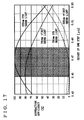
- Fig. 1 is a diagram showing a relation between a pit depth and intensity of reflected light for every laser beam with a different wavelength.
- the intensity of reflected light is the highest with the pit depth of about 105 nm.
- the intensity of reflected light is the highest with the pit depth of about 125 nm.
- reflectance significantly changes with the wavelength of laser beam as organic dye is used for a recording film and a sufficient intensity of reflected light cannot be obtained using a single-wavelength laser with a wavelength of 635 nm.
- the CD-R cannot be suitably reproduced. Therefore, a two wavelengths to beam laser is required for the optical pickup device capable of compatibly reproducing the DVD and the CD-R or the CD-ROM.
- laser beam with a wavelength of 430 nm would be employed due to the trend of shorter wavelength in the near future, such a two wavelengths to beam laser would be even more highly required.
- an object of the present invention to provide an optical pickup device capable of performing recording and/or reproducing for optical disks having substrates with different thicknesses by using a laser beam with two different wavelengths.
- the objective lens is arranged opposite to the first or second optical disk.
- the laser beam generating means selectively generates a first laser beam with a first wavelength and a second laser beam with a second wavelength which is different from the first wavelength.
- the optical device includes: a central region arranged between the objective lens and the laser beam generating means, allowing transmission of the first laser beam without any change and increasing the diameter of the second laser beam by diffraction; and a peripheral region allowing transmission of the first laser beam without any change and substantially shielding the second laser beam by diffraction or absorption.
- a hologram is formed in the central region of the optical device.
- the hologram includes a plurality of annular convex portions each having four steps and coaxially formed, where a height h1 of each step is determined in accordance with the following expressions (1) to (5).
- ⁇ m mth order diffraction efficiency
- ⁇ (x) is a function of phase difference defined by expression (2)
- T is a period of the function of phase difference
- A(x) is transmittance
- ⁇ is the first or second wavelength
- n is refractive index of the annular convex portion
- n0 is refractive index of the periphery of the annular convex portion
- ⁇ 0 is a constant.
- a refraction grating is formed in the peripheral region of the optical device.
- the diffraction grating has varying grating constants.
- the laser beam generating means polarizes the first laser beam in a first direction and the second laser beam in a second direction which is different from the first direction.
- a polarizing filter is formed having a polarizing direction which is perpendicular to the second direction.
- a polarizing glass is formed in the peripheral region of the optical device which absorbs the laser beam with the second wavelength.
- the laser beam generating means is a semiconductor laser including a package and first and second laser chips.
- the first laser chip is arranged within the package and oscillates the first laser beam.
- the second laser beam is arranged within the package and oscillates the second laser beam.
- the optical pickup device moves along two parallel guide shafts provided in a radial direction of the first or second optical disk, and includes a rising mirror and a body.
- the rising mirror is arranged immediately below the objective lens and the optical device, and reflects the first or second laser beam directed from the semiconductor laser in a direction which is parallel to the main surface of the first or second optical disk in a direction which is perpendicular to the main surface of the first or second optical disk.
- the body is supported between the two guide shafts and the objective lens accommodates the optical device, the semiconductor laser and the rising mirror.
- An optical axis of the laser beam entering the rising mirror is angled with respect to a perpendicular relative to the two guide shafts to form an acute angle.
- a line passing emittance openings of the first and second laser chips is angled with respect to the main surface of the first or second optical disk to form an acute angle which is equal to the above mentioned acute angle.
- the optical pickup device further includes a collimator lens arranged between the optical device and the semiconductor laser.
- the first laser chip is spaced by a first distance from the collimator lens such that the first laser beam transmitted through the collimator lens is collimated.
- the second laser chip is spaced by a second distance, which is different from the first distance, from the collimator lens such that the second laser beam transmitted through the collimator lens is collimated.
- the semiconductor laser further includes an optical waveguide.
- the optical waveguide includes a first incident opening facing the emittance opening of the first laser chip, a second incident opening facing the emittance opening of the second laser chip and an emittance opening communicating with the first and second incident openings.
- the first and second laser chips are arranged such that one sides thereof are adjacent to each other.
- the distances between the emittance openings of the first and second laser chips and the one sides are respectively shorter than the distances between the emittance openings and the other sides opposite to the one sides.
- the semiconductor laser further includes a photodetector arranged on the side opposite to the side of emittance of the first and second laser chips for monitoring both the first and second laser beams leaked from the first and second laser chips.
- the semiconductor laser further includes first to fourth terminals.
- the first terminal is connected to one electrodes of the first and second laser chips and the photodetector.
- the second terminal is connected to the other terminal of the second laser chip.
- the third terminal is connected to the other electrode of the second laser chip.
- the fourth terminal is connected to the other electrode of the photodetector.
- the first wavelength is between 620nm and 680nm and the second wavelength is between 765nm and 795nm.
- the objective lens is adapted to the first optical disk and has a numerical aperture of between 0.55 and 0.65.
- the objective lens has an effective numerical aperture of between 0.40 and 0.50 upon incidence of the second laser beam.
- the first laser beam is transmitted through the optical device without any change and focused on a signal recording surface of the first optical disk by the objective lens.
- the periphery of the second laser beam is substantially shielded by the peripheral region of the optical device and the diameter of the central portion of the second laser beam is increased by the central region of the optical device, so that the second laser beam is focused on the signal recording surface of the second optical disk by the objective lens.
- the optical pickup device is capable of performing recording and/or reproducing for the first and second optical disks having substrates with different thicknesses.
- the following table shows a rated value and a reproducing condition for a CD-ROM, a CD-R and a DVD, which are compatibly reproduced by an optical pickup device according to an embodiment of the present invention.
- a thickness of a substrate is 1.2 (with tolerance of ⁇ 0.1)mm
- a minimum pit length is 0.90 (with tolerance of ⁇ 0.1) ⁇ m
- a track pitch is 1.6 (with tolerance of ⁇ 0.1) ⁇ m
- a reflectance is at least 60 % to 70% for a laser beam with a wavelength of 780 nm.
- a spot diameter of the laser beam during reproduction is 1.5 (with tolerance of ⁇ 0.1) ⁇ m
- a numerical aperture of an objective lens is 0.45 (with tolerance of ⁇ 0.05)
- a wavelength of the laser beam is 780 (with tolerance of ⁇ 15)nm.
- the CD-R has the same thickness of substrate, minimum pit length, track pitch, reflectance, spot diameter during reproduction, numerical aperture of objective lens and wavelength of laser beam as those for the above mentioned CD-ROM.
- a thickness of substrate is 0.6 (with tolerance of ⁇ 0.05)mm
- a minimum pit length is 0.40 (with tolerance of ⁇ 0.1) ⁇ m
- a track pitch is 0.74 (with tolerance of ⁇ 0.01) ⁇ m
- a reflectance is at least 70% (in the case of one layer DVD) or at least 20 % to 40% (in the case of two layered DVD) for a laser beam with a wavelength of 635 nm.
- a spot diameter of the laser beam during reproduction is 0.9 (with tolerance of ⁇ 0.5) ⁇ m
- a numerical aperture of an objective lens is 0.60 (with tolerance of ⁇ 0.05) and a wavelength of the laser beam is 635 (with tolerance of 620 to 680)nm.
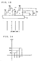
- an optical pickup device 10 includes: an objective lens 7 arranged opposite to an optical disk; a semiconductor laser 1 selectively generating laser beams with wavelengths of 635 (with tolerance of ⁇ 15)nm and 780 (with tolerance of ⁇ 15)nm; an optical device 5 arranged immediately below objective lens 7; an actuator 6 holding both objective lens 7 and optical device 5; a mirror 4 arranged immediately below objective lens 7 and optical device 5 for reflecting a laser beam directed from semiconductor laser 1 in a direction parallel to a main surface of the optical disk in a direction perpendicular to the main surface of the optical disk; a half mirror 2 perpendicularly reflecting the laser beam directed from semiconductor laser 1 toward rising mirror 4; a collimator lens 3 arranged between rising mirror 4 and half mirror 2 for collimating the laser beam directed from semiconductor laser 1; and a photodetector 8 receiving the laser beam reflected by the optical disk.
- half of the laser beam emitted from semiconductor laser 1 is reflected by half mirror 2 toward collimator lens 3 for collimation and raised by rising mirror 4.
- the raised laser beam is collected by objective lens 7 through optical device 5 and focused on a signal recording surface 9a or 99a through a transparent substrate 9 of the DVD or a transparent substrate 99 of the CD including polycarbonate.
- the laser beam reflected by signal recording surface 9a or 99a travels back to half mirror 2 through transparent substrate 9 or 99, objective lens 7, optical device 5, mirror 4 and collimator lens 3.
- Half of the laser beam is transmitted through half mirror 2 and detected by photodetector 8.
- objective lens 7 is adapted to the DVD and has a numerical aperture of 0.60 (with tolerance of ⁇ 0.05). In other words, objective lens 7 is designed to focus the collimated laser beam with the wavelength of 635 nm on signal recording surface 9a of the DVD.
- Semiconductor laser 1 further includes laser chips 1a and 1b oscillating laser beams with the wavelengths of 635 nm and 780 nm, respectively.
- laser chip 1a is activated by a semiconductor laser driving circuit 18.
- laser chip 1b is activated by semiconductor laser driving circuit 18.
- optical pickup device 10 further includes a servo mechanism 13 performing focusing control and tracking control for objective lens 7.
- the focusing control allows objective lens 7 to be perpendicularly moved with respect to the main surface of the optical disk such that the laser beam is always focused on signal recording surface 9a or 99a.
- the tracking control allows objective lens 7 to be perpendicularly moved with respect to the direction in which a track is moved such that the laser beam is always directed on the track.
- An optical disk reproducing apparatus using the above mentioned optical pickup device 10 includes a preamplifier 11, a servo circuit 12, a determining circuit 14, an instructing circuit 15, an RF demodulating circuit 16, a characteristic switching circuit 17, semiconductor laser driving circuit 18 and a control circuit 19.
- Photodetector 8 detects the laser beam reflected by signal recording surface 9a or 99a to generate a reproduced signal, which is then applied to preamplifier 11.
- the reproduced signal is applied to determining circuit 14, the RF demodulating circuit and servo circuit 12 after it is amplified by preamplifier 11.
- Servo circuit 12 controls a servo mechanism 13 in response to a focusing error signal and a tracking error signal of the applied reproduced signal 10.
- determining circuit 14 identifies the type (the DVD, CD-ROM or CD-R) of the optical disk mounted to the apparatus in response to the applied reproduced signal, and applies the identification result to instructing circuit 15.
- Instructing circuit 15 switches laser chips 1a and 1b of semiconductor laser 1 for adapting to the identified optical disk and thus applies an instruction to control circuit 19 in accordance with the applied identification result.
- As instructing circuit 15 also switches RF demodulating circuit 16 for adapting to reproduction of the identified optical disk and thus applies an instruction also to characteristic switching circuit 17 in accordance with the applied identification result.
- Control circuit 19 controls semiconductor laser driving circuit 18 such that laser chips 1a and 1b are switched in accordance with the instruction from instructing circuit 15.
- Characteristic switching circuit 17 switches the characteristic of RF demodulating circuit 16 for performing reproduction suitable for the optical disk mounted to the apparatus in accordance with the instruction from instructing circuit 15.
- semiconductor laser 1 includes, in addition to laser chips 1a and 1b, a base 1c to which these laser chips 1a and 1b are mounted, and a package 1d for accommodating laser chips 1a and 1b and base 1c.
- Three notches k1, k2 and k3 are formed in package 1d and laser chips 1a and 1b are mounted such that their emittance openings PA and PB are arranged on an imaginary line between notches k2 and k3.
- Semiconductor laser 1 is positioned such that the spots which are formed by laser beams from laser chips 1a and 1b on signal recording surface 9a or 99a are symmetrically arranged on either side of the track. More specifically, semiconductor laser 1 is positioned such that the direction of k2-k3 corresponds to the direction of tracking (the radial direction) of the optical disk. The arrangement will be later described in detail.
- laser chips 1a and 1b are separately manufactured and mounted to base 1c, they may also be manufactured together by crystal growth on a single semiconductor substrate.
- a distance L between emittance openings PA and PB of laser chips 1a and 1b is for example between 100 ⁇ m and 500 ⁇ m.
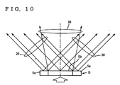
- optical device 5 has a central region 5b in a round shape and a peripheral region 5a thereof.
- Central region 5b allows transmission of the laser beam with the wavelength of 635 nm without any change and increases a diameter of the laser beam with the wavelength of 780 run by diffraction.
- a hologram 20 is formed in central region 5b.
- peripheral region 5a allows transmission of the laser beam with the wavelength of 635 nm without any change and substantially shields the laser beam with the wavelength of 780 run by diffraction. Therefore, a diffraction grating 21 is formed in peripheral region 5a.
- hologram 20 in central region 5b includes a coaxially formed plurality of annular convex portions 22.
- Each annular convex portion 22 has four steps 22a.
- Pitches P1 of annular convex portions 22 become narrower as closer to the peripheral region so that hologram 20 is provided with a lens effect.
- a height of each step 22a is determined so that hologram 20 functions as a lens only for the laser beam with the wavelength of 780 nm. The height of each step 22a will later be described in detail.
- diffraction grating 21 in peripheral region 5a includes a plurality of convex portions in a striped pattern (hereinafter referred to as striped convex portions) 23 which are formed in the same direction.
- striped convex portions 23 are formed with constant pitches P2 (preferably between 8 ⁇ m and 12 ⁇ m)
- diffraction grating 21 has the same diffraction constants.
- a height of striped convex portion 23 is also determined such that diffraction grating 21 functions only for the laser beam with the wavelength of 780 nm. The height of striped convex portion 23 will also be later described in detail. It is noted that optical device 5 with such structure can readily be manufactured by etching a glass 24.
- a collimated laser beam 25 with the wavelength of 635 nm enters optical device 5
- the entered laser beam 25 is transmitted through optical device 5 without any diffraction. This is because optical device 5 does not function at all for laser beam 25 with the wavelength of 635 nm.
- the transmitted laser beam 25 enters and is collected by objective lens 7 and is focused on signal recording surface 9a of DVD 26. It is noted that in Fig. 7, a part of a cross section of optical device 5 is shown in enlargement.
- -first order diffraction beam 30 due to diffraction grating 21 travels toward the right with respect to laser beam 28 in the drawing.
- only laser beam 28 which has been transmitted through central region 5b of optical device 5 is transmitted to and collected by objective lens 7 and is focused on signal recording surface 99a of the CD-ROM.
- laser beams 29 and 30 which have been transmitted through peripheral region 5a of optical device 5 are greatly diffracted by diffraction grating 21 formed in peripheral region 5a, they do not enter objective lens 7.
- the periphery of laser beam 27 with the wavelength 780 nm, which has been transmitted to optical device 5 is substantially shielded by peripheral region 5a of optical device 5.
- laser beam 28 transmitted through optical device 5 and traveling outwardly while increasing its diameter is -first order diffraction beam LB-1.
- -first order diffraction beam LB-1 there are 0th order diffraction beam LB0, +first order diffraction beam (not, shown) or the like.
- the intensity of such diffraction beam is kept as low as possible.
- the outwardly traveling -first order diffraction beam LB-1 is employed due to the following reason.
- a diameter of central region 5b of optical device 5 and a shape of hologram 20 formed in central region 5b are determined such that an effective numerical aperture of objective lens 7 for 0th order diffraction beam LB0 and -first order diffraction beam LB-1 is 0.45. It is noted that, in Fig. 8, a part of the cross section of optical device 5 is shown in enlargement.
- Optical device 5 is fixed to actuator 6 for holding objective lens 7 as shown in Fig. 2.
- Actuator 6 is connected to servo mechanism 13 shown in Fig. 3.
- Servo mechanism 13 is responsive to a focusing error signal from photodetector 8 for moving actuator 6 in a direction of an optical axis, and is responsive to a tracking error signal from photodetector 28 for moving actuator 6 in the radial direction of the optical disk.
- optical device 5 is thus fixed to objective lens 7, it moves along with objective lens 7.
- optical device 5 substantially shields the periphery of laser beam 27 with the wavelength of 780 nm and diffracts the central portion of laser beam 27 outwardly to increase its diameter, thereby focusing laser beam 27 on signal recording surface 99a of CD-ROM 31.
- optical device 5 allows transmission of the laser beam with the wavelength of 635 nm without any diffraction, thereby focusing laser beam 25 on signal recording surface 9a of DVD 26.
- a function of phase difference ⁇ (x) as shown in Fig. 14 is assumed.
- T of the function of phase difference is significantly large as compared with a wavelength ⁇ of the laser beam and a thickness of the diffraction region
- mth order diffraction efficiency ⁇ m is generally provided in accordance with the following expression (1).
- ⁇ m 1 T 0 T A(x)exp ⁇ i ⁇ (x) ⁇ exp -i 2 ⁇ mx T dx 2
- A(x) is a transmittance at x.
- phase difference ⁇ (x) shown in Fig. 14 is provided in accordance with the following expressions (2).
- n is a refractive index of the material of annular convex portion 22 in hologram 20 and n0 is a refractive index in the vicinity of annular convex portion 22 (usually a retractive index of air).
- ⁇ 635 nm
- height h1 is determined such that 0th order diffraction beam of the laser beam with the wavelength of 635 nm and -first order diffraction beam of the laser beam with the wavelength of 780 nm are large. As shown in Fig. 17, for example, height h1 must be between 0.448 ⁇ m and 0.482 ⁇ m to make 0th order diffraction efficiency ⁇ 0 for the wavelength of 635 nm at least 90% and -first order diffraction efficiency ⁇ -1 for the wavelength of 780 nm at least 70%.
- Height h2 is determined in accordance with the following expression (6).
- m is an integer
- ⁇ is a wavelength of a laser beam to be transmitted without any diffraction
- n is a refractive index of a material for striped convex portion 23 in diffraction grating 21
- n0 is a refractive index in the vicinity of striped convex portion 23 (usually a refractive index of air).
- h2 m ⁇ ⁇ /(n - n0)
- diffraction grating 21 with wavelength selectivity which allows transmission of the laser beam with the wavelength of 635 nm without any diffraction and allows diffraction of the laser beam with the wavelength of 780 nm, is formed.
- diffraction grating 21 may be provided with wavelength selectivity by forming on diffraction grating 21 a film of cyanine dye having a refractive index which changes with a wavelength.
- Cyanine dye has a refractive index of 1.50 for the laser beam of the wavelength of 635 nm and a refractive index of 1.65 for the laser beam with the wavelength of 780 nm.
- diffraction grating 21 formed of glass has a refractive index of 1.50 for the laser beam of the wavelength of either 635 nm or 780 nm.
- the diffraction grating does not function for the laser beam with the wavelength of 635 nm. Accordingly, the diffraction grating with wavelength selectivity, which allows diffraction of the laser beam with the wavelength of 780 nm but not of the laser beam with the wavelength of 635 nm, is formed.
- laser chip 1a is activated by semiconductor laser driving circuit 18 as shown in Fig. 18.
- semiconductor laser driving circuit 18 As shown in Fig. 18.
- half of the laser beam with the wavelength of 635 nm emitted from semiconductor laser 1 is reflected by half mirror 2, collimated by collimator lens 3, raised by mirror 4 and transmitted through optical device 5 without any diffraction.
- the transmitted laser beam is transmitted to and collected by objective lens 7 and focused on signal recording surface 9a through transparent substrate 9 of the DVD.
- a spot diameter of the laser beam on the signal recording surface is 0.9 (with tolerance of ⁇ 0.1) ⁇ m.
- laser chip 1b is activated by semiconductor laser driving circuit 18.
- half of the laser beam with the wavelength of 780 nm emitted from semiconductor laser 1 is reflected by half mirror 2, collimated by collimator lens 3, raised by rising mirror 4.
- the periphery of the laser beam is substantially shielded by optical device 5 and only central portion thereof is increased in diameter by diffraction.
- the laser beam transmitted through central region 5b of optical device 5 is transmitted to and collected by objective lens 7 and focused on signal recording surface 99a through transparent substrate 99 of the CD-R or CD-ROM.
- a spot diameter of the laser beam on signal recording surface 99a is 1.5 (with tolerance of ⁇ 0.1) ⁇ m.
- hologram 20 is formed for allowing transmission of the laser beam with the wavelength of 635 nm through the central region of optical device 5 arranged immediately below objective lens 7 without any diffraction and for increasing the diameter of the laser beam with the wavelength of 780 nm by diffraction.
- diffraction grating 21 is formed for allowing transmission of the laser beam with the wavelength of 635 nm through peripheral region 5a of optical device 5 without any diffraction and for substantially shielding the laser beam with the wavelength of 780 nm by diffraction.
- the optical pickup device is capable of compatibly reproducing the DVD, CD-R and CD-ROM.
- the optical pickup device employs the laser beam with the wavelength of 635 nm which is the most suitable for the DVD and also employs the laser beam with the wavelength of 780 nm which is the moot suitable for the CD-R or CD-ROM.
- the optical pickup device can suitably reproduce any of the DVD, CD-R and CD-ROM.
- the optical pickup device is manufactured by simply adding to the conventional optical pickup device one optical device 5 having both hologram 20 and diffraction grating 21. Therefore, the optical pickup device can be manufactured almost in the same size as that of the conventional optical pickup device.
- optical device 5 is fixed to objective lens 7, accurate focusing of the laser beam on the signal recording surface can be achieved even if objective lens 7 is moved for focusing and tracking.
- optical device 5 does not have any part which would be electrically or mechanically influenced, it is less susceptible to breakdown.
- annular convex portion 22 of hologram 20 formed in central region 5b of the above mentioned optical device 5 has steps on the inner side as shown in Fig. 6, it may have steps on the outer side as shown in Fig. 20.
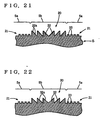
- annular convex portion 22 of the above mentioned hologram 20 has four steps 22a as shown in Fig. 6, it may have seven steps as shown in Fig. 21 and, the number of the steps is not particularly limited.
- annular convex portion 22 of hologram 20 has a plurality of steps
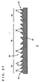
- annular convex portion 32 having an inclined surface 32a instead of steps may be formed.
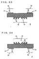
- hologram 20 and diffraction grating 21 are formed on the same surface in the above mentioned optical device 5, as shown in Figs. 23 and 24, they may be formed on mutually opposed surfaces.
- the diffraction grating may be formed on the surface on the side of objective lens 7 and hologram 20 on the surface on the opposite side as shown in Fig. 23, or hologram 20 may be formed on the surface on the side of objective lens 7 and diffraction grating 21 on the surface on the opposite side as shown in Fig. 24.
- optical device 5 can more easily be manufactured by thus forming hologram 20 and diffraction grating 21 on the different surfaces.
- hologram 20 formed of annular convex portion 32 having inclined surface 32a
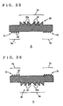
- hologram 20 and diffraction grating 21 may be formed on the mutually opposed surfaces as shown in Figs. 25 and 26.
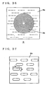
- hologram 33 may also be formed in peripheral region 5a as shown in Fig. 27.
- Annular convex portions 22 of hologram 33 in peripheral region 5a are coaxially formed in a similar manner as those of hologram 20 in central region 5b, but with prescribed pitches P3.
- hologram 33 is also formed in peripheral region 5a, so that all of the laser beam transmitted to peripheral region 5a would be outwardly diffracted and not inwardly diffracted to enter objective lens 7. As a result, noise due to the inwardly diffracted laser beam is reduced.
- annular convex portion 22 shown in Fig. 27 has steps on the inner side, it may also have steps on the outer side as shown in Fig. 28.
- diffraction grating 21 of optical device 5 has the same grating constants, it may have varying diffraction constants as shown in Fig. 29. More specifically, the pitches of the striped convex portions of the diffraction grating formed in peripheral region 5a of optical device 5 may gradually become narrower from the right to left side in the drawing.
- peripheral region 5a of optical device 5 needs only substantially shield the laser beam with the wavelength of 780 nm and a polarizing filter may be formed in peripheral region 34a of optical device 34 as shown in Fig. 34.
- a hologram is formed in central region 34b of optical device 34 in a similar manner as described above.
- the polarizing filter formed in peripheral region 34a has a polarization direction in a longitudinal direction of the drawing as shown in Fig. 35.
- peripheral region 34a allows transmission of the laser beam polarized in the longitudinal direction of the drawing without any diffraction, but shields the laser beam polarized in a transverse direction in the drawing by reflectance.
- semiconductor laser 1 In the optical pickup device having such optical device 34, semiconductor laser 1 must polarize the laser beam with the wavelength of 635 nm in the longitudinal direction of the drawing and the laser beam with the wavelength of 780 nm in the transverse direction in the drawing. Thus, while all of the laser beam with the wavelength of 635 nm is transmitted through optical device 34, the periphery of the laser beam with the wavelength of 780 nm is shielded by peripheral region 34a and only central portion thereof is diffracted by the hologram and reaches objective lens 7 while increasing its diameter.
- a polarizing glass may be formed in peripheral region 35a of optical device 35.
- a hologram is formed in central region 35b of optical device 35 as in the case described above.
- the polarizing glass is obtained by burning a glass surface on which silver atoms are applied in elongate shapes as shown in Fig. 37 for absorption of the laser beam with the wavelength of 780 nm.
- An aspect ratio R1/R2 of the applied silver atoms is between 1 and 5.
- aspect ratio R1/R2 is set to absorb only the laser beam with the wavelength of 780 nm.
- optical device 35 when such optical device 35 is employed, all of the laser beam with the wavelength of 635 nm is transmitted through optical device 35, whereas the periphery of the laser beam with the wavelength of 780 nm is shielded by the polarizing glass and the central portion thereof is diffracted to reach objective lens 7 while increasing its diameter.
- a colored glass for absorbing the laser beam with the wavelength of 780 nm may be employed in place of the polarizing glass.
- the central region of the optical device selectively causes a diffraction phenomenon in accordance with the wavelength of the laser beam
- the present invention is not limited to this and the central region of the optical device may selectively cause diffraction phenomenon in accordance with a plane of polarization of the laser beam. More specifically, the central region of the optical device may diffract only laser beam polarized in the transverse direction in the drawing and not the laser beam polarized in the longitudinal direction in the drawing.
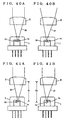
- a focal length for collimator lens 3 including a single material varies in accordance with the wavelength of the laser beam. More specifically, the focal length of collimator lens 3 for the wavelength of 780 nm is longer by 0.15 mm than that for the wavelength of 635 nm. Such variation in focal distances way cause chromatic aberration.
- a laser beam 25 with the wavelength of 635 nm emitted from laser chip 1a is transmitted through and collimated by collimator lens 3 as shown in Fig. 40A.
- a laser beam 27 with the wavelength of 780 nm emitted from laser chip 1b is not collimated even after it is transmitted through collimator lens 3 as shown in Fig. 40B.
- laser beam 27 with the wavelength of 780 nm is not accurately focused on the signal recording surface of the CD-R or CD-ROM by objective lens 7, whereby chromatic aberration is caused.
- laser chip 1a is spaced by a first focal length F1 from the collimator lens such that laser beam 25 with the wavelength of 635 nm is transmitted through and collimated by collimator lens 3, and laser chip 1b is spaced by a second focal length F2 which is longer than first focal length F1 by 0.15 mm from collimator lens 3 such that the laser beam with the wavelength of 780 nm is transmitted through and collimated by collimator lens 3 as shown in Fig. 41B.
- a beam splitter 36 is arranged between optical device 5 and collimator lens 3 in place of half mirror 2.
- a collecting lens 37 is arranged between beam splitter 36 and photodetector 8 for collecting the laser beam from beam splitter 36 to photodetector 8.
- semiconductor laser 31 has an optical waveguide 39 for combining the laser beams with the wavelengths of 635 nm and 780 nm.
- Optical waveguide 39 is in a shape of Y as shown in Fig. 43, and includes two incident openings facing the emittance openings of laser chips 1a and 1b respectively, and an emittance opening communicating with these two incident openings.
- semiconductor laser 38 luminous points of the laser beams with the wavelengths of 635 nm and 780 nm are substantially the same, so that displacement of optical axes is prevented.
- a prescribed distance PL1 is provided between their emission points PA and PB as shown in Fig. 45.
- Distance PL1 corresponds to a width of laser chips 1a and 1b, which is generally between 300 ⁇ m and 350 ⁇ m. As displacement of emittance openings PA and PB may cause aberration, distance PL1 is preferably made as small as possible.
- emission points PA and PB are preferably formed offset from the centers of laser chips 1a and 1b to reduce distance PL2 therebetween.
- a distance PL3 between emission points PA and PB may be reduced by cutting the side ends of laser chips 1a and 1b which are adjacent to each other.
- laser chips 1a and 1b are arranged with their one sides adjacent to each other, and the distances between emission points PA and PB and one sides thereof are shorter than those between emission points PA and PB and the other sides opposite to the one sides, respectively.
- semiconductor laser 1 must be provided with a photodetector for monitoring the laser beam emitted therefrom.
- two photodetectors may be provided corresponding to laser chips 1a and 1b.
- a single photodetector 44 is preferably provided for monitoring laser beams with the wavelengths of 635 nm and 780 nm leaking from the backsides of laser chips 1a and 1b.
- Semiconductor laser 1 has four terminals 45 to 48. As shown in Fig. 49A, terminal 45 is connected to anode electrodes of laser chips 1a and 1b and a cathode electrode of photodetector 44. Terminal 46 is connected to a cathode electrode of laser chip 1a. Terminal 47 is connected to a cathode electrode of laser chip 1b. Terminal 48 is connected to an anode electrode of photodetector 44. As terminal 45 is connected to one electrodes of laser chips 1a and 1b and photodetector 44, the number of terminals for semiconductor laser 1 is reduced.
- terminals 45 and 48 may also be connected to the anode and cathode electrodes of photodetector 44, respectively.
- terminal 45 is connected to cathode electrodes of laser chips 1a and 1b and photodetector 44, terminal 46 to the anode electrode of laser chip 1a, terminal 47 to the anode electrode of laser chip 1b and terminal 48 to the anode electrode of photodetector 44.
- terminal 45 may be connected to the cathode electrodes of laser chips 1a and 1b and the anode electrode of photodetector 44, terminal 46 to the anode electrode of laser chip 1a, terminal 47 to the anode electrode of laser chip 1b and terminal 48 to the cathode electrode of photodetector 44.
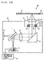
- Fig. 50 is a top view showing only an optical system of the above described optical pickup device. It is noted that, in Fig. 50, a diffraction grating 40 for a three-beam method is arranged between semiconductor laser 1 and half mirror 2. In addition, a Wollaston prism 41 for collecting the laser beam with the wavelength of 635 nm or 780 nm in a prescribed position on photodetector 8 is arranged between half mirror 2 and photodetector 8.
- objective lens 7 and optical device 5 are shown on the upper side of mirror 4 in Fig. 50, they are arranged immediately above mirror 4. In other words, an optical axis of objective lens 7 is perpendicular to, not parallel to, an optical axis of semiconductor laser 1.
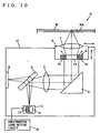
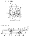
- the optical system shown in Fig. 50 is accommodated in body 42 as shown in Fig. 51A.
- body 42 is supported between two guide shafts 43.
- the optical pickup device including such optical system and body 42 can move in the radial direction of the optical disk along guide shafts 43.
- objective lens 7 can be moved in a direction toward or away from a driving axis (a center of the optical disk) of a spindle motor 44.
- an optical axis LN1 of the laser beam entering mirror 4 is aligned with a perpendicular LN2 with respect to two guide shafts 43, so that a relatively long distance GL1 is ensured between guide shafts 43.
- the optical system is desirably arranged such that optical axis LN1 of the laser beam entering mirror 4 is angled with respect to perpendicular LN2 for two guide shafts 43 to form an acute angle ⁇ (of for example between 30° and 45°).
- ⁇ of for example between 30° and 45°.
- the laser beams with the wavelengths of 635 nm and 780 nm from laser chips 1a and 1b can form beam spots symmetrically on either side of the track of the optical disk, respectively.
- package 1d of semiconductor laser 1 shown in Fig. 52B is provided with a notch 1e which is parallel to the upper and lower surfaces of body 42. With such notch 1e formed in package 1d of semiconductor laser 1, a thickness T2 is obtained for body 42 which is smaller than a thickness T1 of body 42 shown in Fig. 51B.
- optical pickup device is mainly directed for reproduction, it may also be directed for recording, or both recording and reproduction.
Abstract
Description
- The present invention relates to optical pickup devices and, more specifically, to an optical pickup device performing recording and/or reproducing for a digital video disk (a DVD) and a compact disk (a CD).
- An optical disk with a thickness of about 1.2 mm, such as a CD-ROM (Compact Disk-Read Only Memory), has been provided for reading information using a semiconductor laser. In this type of optical disk, by performing focusing servo control and tracking servo control for an objective lens for pickup, a pit string of a signal recording surface is irradiated with laser beam to reproduce a signal. Recently, such optical disks are increasingly becoming higher in density for recording an animation lasting for a long period of time.
- For example, a DVD standard has been proposed for recording information of 4.7 G bytes on one side of the optical disk having a diameter of 12 cm, which is the same as that of the CD-ROM. A transparent substrate of the DVD has a thickness of about 0.6 mm. A single DVD, which has two such transparent substrates applied to each other back to back, can record information of 9.4 G bytes. Further, as a write-once optical disk having the same diameter, thickness of substrate and recording density as those for the CD-ROM, there exists a CD-R (Compact Disk-Recordable).
- Since three different types of optical disks, including the DVD, the CD-ROM and the CD-R, would exist in the same apparatus in the near future, a device capable of compatibly reproducing these three different types of optical disks is required. The DVD and the CD-ROM or the CD-R, however, cannot be reproduced by a single optical pickup device because of the difference in thicknesses of the transparent substrates.
- Then, in Japanese Patent Laying-Open No. 5-303766, an apparatus has been proposed which allows reproduction of a high density optical disk having a thin transparent substrate with a thickness of 0.6 mm and a standard density optical disk having a standard transparent substrate with a thickness of 1.2 mm by using a single optical pickup device. In the apparatus, an objective lens with a numerical aperture of 0.6 is employed which has been designed to reproduce the high density optical disk by a laser beam with a short wavelength. When the standard density optical disk is to be reproduced, an aspherical optical device is inserted on the side of a light source of the objective lens which is provided with an aperture for shielding the periphery of laser beam to decrease an effective numerical aperture of the objective lens.
- Moreover, to change the effective numerical aperture of an objective lens selectively shielding the periphery of laser beam emitted from a semiconductor laser to collect laser beam, an apparatus has been disclosed in Japanese Patent Laying-Open No. 8-321065 which is provided with a liquid crystal selectively rotating the plane of polarization of laser beam and a polarizing plate allowing transmission of only laser beam which is polarized in a specific direction, and which can compatibly reproduce optical disks having substrates with different thicknesses. While the apparatus can compatibly reproduce the DVD and the CD-ROM having substrates of different thicknesses, it cannot reproduce the CD-R as a laser beam with a wavelength of 635 nm is employed. The reason is as follows.
- Fig. 1 is a diagram showing a relation between a pit depth and intensity of reflected light for every laser beam with a different wavelength. As shown in Fig. 1, when the laser beam with a wavelength of 635 nm is employed, the intensity of reflected light is the highest with the pit depth of about 105 nm. On the other hand, when laser beam with a wavelength of 780 nm is employed, the intensity of reflected light is the highest with the pit depth of about 125 nm. In the case of the CD-R, reflectance significantly changes with the wavelength of laser beam as organic dye is used for a recording film and a sufficient intensity of reflected light cannot be obtained using a single-wavelength laser with a wavelength of 635 nm. Thus, the CD-R cannot be suitably reproduced. Therefore, a two wavelengths to beam laser is required for the optical pickup device capable of compatibly reproducing the DVD and the CD-R or the CD-ROM. When laser beam with a wavelength of 430 nm would be employed due to the trend of shorter wavelength in the near future, such a two wavelengths to beam laser would be even more highly required.
- Therefore, it is an object of the present invention to provide an optical pickup device capable of performing recording and/or reproducing for optical disks having substrates with different thicknesses by using a laser beam with two different wavelengths.
- According to the present invention, an optical pickup device performing recording and/or reproducing for a first optical disk having a first transparent substrate and a second optical disk having a second transparent substrate with a thickness which is smaller than that of the first transparent substrate includes an objective lens, a laser beam generating means and an optical device. The objective lens is arranged opposite to the first or second optical disk. The laser beam generating means selectively generates a first laser beam with a first wavelength and a second laser beam with a second wavelength which is different from the first wavelength. The optical device includes: a central region arranged between the objective lens and the laser beam generating means, allowing transmission of the first laser beam without any change and increasing the diameter of the second laser beam by diffraction; and a peripheral region allowing transmission of the first laser beam without any change and substantially shielding the second laser beam by diffraction or absorption.
- Preferably, a hologram is formed in the central region of the optical device.
- More preferably, the hologram includes a plurality of annular convex portions each having four steps and coaxially formed, where a height h1 of each step is determined in accordance with the following expressions (1) to (5).if m = 0

- Here, ηm is mth order diffraction efficiency, (x) is a function of phase difference defined by expression (2), T is a period of the function of phase difference, A(x) is transmittance, λ is the first or second wavelength, n is refractive index of the annular convex portion, n0 is refractive index of the periphery of the annular convex portion and 0 is a constant.
- Preferably, a refraction grating is formed in the peripheral region of the optical device.
- More preferably, the diffraction grating has varying grating constants.
- Preferably, the laser beam generating means polarizes the first laser beam in a first direction and the second laser beam in a second direction which is different from the first direction. In the peripheral region of the optical device, a polarizing filter is formed having a polarizing direction which is perpendicular to the second direction.
- Preferably, a polarizing glass is formed in the peripheral region of the optical device which absorbs the laser beam with the second wavelength.
- Preferably, the laser beam generating means is a semiconductor laser including a package and first and second laser chips. The first laser chip is arranged within the package and oscillates the first laser beam. The second laser beam is arranged within the package and oscillates the second laser beam.
- More preferably, the optical pickup device moves along two parallel guide shafts provided in a radial direction of the first or second optical disk, and includes a rising mirror and a body. The rising mirror is arranged immediately below the objective lens and the optical device, and reflects the first or second laser beam directed from the semiconductor laser in a direction which is parallel to the main surface of the first or second optical disk in a direction which is perpendicular to the main surface of the first or second optical disk. The body is supported between the two guide shafts and the objective lens accommodates the optical device, the semiconductor laser and the rising mirror. An optical axis of the laser beam entering the rising mirror is angled with respect to a perpendicular relative to the two guide shafts to form an acute angle.
- More preferably, a line passing emittance openings of the first and second laser chips is angled with respect to the main surface of the first or second optical disk to form an acute angle which is equal to the above mentioned acute angle.
- Preferably, the optical pickup device further includes a collimator lens arranged between the optical device and the semiconductor laser. The first laser chip is spaced by a first distance from the collimator lens such that the first laser beam transmitted through the collimator lens is collimated. The second laser chip is spaced by a second distance, which is different from the first distance, from the collimator lens such that the second laser beam transmitted through the collimator lens is collimated.
- Preferably, the semiconductor laser further includes an optical waveguide. The optical waveguide includes a first incident opening facing the emittance opening of the first laser chip, a second incident opening facing the emittance opening of the second laser chip and an emittance opening communicating with the first and second incident openings.
- Preferably, the first and second laser chips are arranged such that one sides thereof are adjacent to each other. The distances between the emittance openings of the first and second laser chips and the one sides are respectively shorter than the distances between the emittance openings and the other sides opposite to the one sides.
- Preferably, the semiconductor laser further includes a photodetector arranged on the side opposite to the side of emittance of the first and second laser chips for monitoring both the first and second laser beams leaked from the first and second laser chips.
- Preferably, the semiconductor laser further includes first to fourth terminals. The first terminal is connected to one electrodes of the first and second laser chips and the photodetector. The second terminal is connected to the other terminal of the second laser chip. The third terminal is connected to the other electrode of the second laser chip. The fourth terminal is connected to the other electrode of the photodetector.
- Preferably, the first wavelength is between 620nm and 680nm and the second wavelength is between 765nm and 795nm.
- Preferably, the objective lens is adapted to the first optical disk and has a numerical aperture of between 0.55 and 0.65.
- Preferably, the objective lens has an effective numerical aperture of between 0.40 and 0.50 upon incidence of the second laser beam.
- Thus, in recording and/or reproducing of the first optical disk, the first laser beam is transmitted through the optical device without any change and focused on a signal recording surface of the first optical disk by the objective lens. On the other hand, in recording and/or reproducing of the second optical disk, the periphery of the second laser beam is substantially shielded by the peripheral region of the optical device and the diameter of the central portion of the second laser beam is increased by the central region of the optical device, so that the second laser beam is focused on the signal recording surface of the second optical disk by the objective lens. Thus, the optical pickup device is capable of performing recording and/or reproducing for the first and second optical disks having substrates with different thicknesses.
-
- Fig. 1 is a diagram showing a relation between a pit depth of an optical disk and intensity of light reflected therefrom for every laser beam with a different wavelength.
- Fig. 2 is a diagram showing a structure of an optical pickup device in accordance with an embodiment of the present invention.
- Fig. 3 is a block diagram showing an overall arrangement of an optical disk reproducing apparatus including the optical pickup device shown in Fig. 1.
- Fig. 4 is a top view showing a structure of a semiconductor laser shown in Fig. 2.
- Fig. 5 is a top view of an optical device shown in Fig. 2.
- Fig. 6 is a cross sectional view of the optical device shown in Fig. 5.
- Fig. 7 is a diagram showing an optical path when a laser beam with a wavelength of 635 nm enters the optical device shown in Figs. 5 and 6.
- Figs. 8 to 12 are diagrams showing optical paths when a laser beam with a wavelength of 780 nm enters the optical device shown in Figs. 5 and 6.
- Fig. 13 is a cross sectional view showing in enlargement a central region of the optical device shown in Fig. 6.
- Fig. 14 is a diagram showing a function of phase difference used for determining a height of each step of annular convex portions in a hologram shown in Fig. 13.
- Fig. 15 is a diagram showing a relation between a height of each step of annular convex portions in the hologram and 0th and ± first order diffraction efficiencies for the laser beam with the wavelength of 635 nm.
- Fig. 16 is a diagram showing a relation between a height of each step of annular convex portions in the hologram and 0th and ± first order diffraction efficiencies for the laser beam with the wavelength of 780 nm.
- Fig. 17 is a diagram collectively showing the diffraction efficiencies shown in Figs. 15 and 16 for determining the height of each step of annular convex portions.
- Fig. 18 is a diagram showing an optical path of the laser beam with the wavelength of 635 nm in reproducing a DVD by the optical pickup device shown in Fig. 2.
- Fig. 19 is a diagram showing an optical path of the laser beam with the wavelength of 780 nm in reproducing a CD-R or a CD-ROM by the optical pickup device shown in Fig. 2.
- Fig. 20 is a diagram showing one modification of the optical device shown in Fig. 6.
- Figs. 21 to 28 are cross sectional views showing another modifications of the optical device.
- Fig. 29 is a top view showing still another modification of the optical device.
- Figs. 30 to 33 are diagrams showing optical paths when the laser beam with the wavelength of 780 nm enters the optical device shown in Fig. 29.
- Fig. 34 is a top view showing still another modification of the optical device.
- Fig. 35 is a diagram showing a polarizing direction of a polarizing filter formed in the peripheral region shown in Fig. 34.
- Fig. 36 is a top view showing still another modification of the optical device.
- Fig. 37 is a diagram partially showing in enlargement a polarizing glass in the peripheral region of the optical device shown in Fig. 36.
- Fig. 38 is a diagram showing an optical system of the optical pickup device according to an embodiment of the present invention.
- Fig. 39 is a diagram showing a relation between a focal length and a wavelength of a collimator lens shown in Fig. 38.
- Fig. 40A is a diagram showing an optical path when the laser beam with the wavelength of 635 nm enters the collimator lens, and Fig. 40B is a diagram showing an optical path when the laser beam with the wavelength of 780 nm enters the collimator lens.
- Fig. 41A is a diagram showing a modification of the semiconductor laser with an optical path when the laser beam with the wavelength of 635 nm enters the collimator lens, and Fig. 41B is a diagram showing an optical path when the laser beam with the wavelength of 780 nm enters the collimator lens from the semiconductor laser shown in Fig. 41A.
- Fig. 42 is a diagram showing a modification of the semiconductor laser with an optical system of the optical pickup device.
- Fig. 43 is a diagram showing a structure of the semiconductor laser shown in Fig. 42.
- Fig. 44A is a side view showing a modification of the semiconductor laser, and Fig. 44B is a top view of the semiconductor laser shown in Fig. 44A.
- Fig. 45 is a diagram showing an arrangement of two laser chips in the semiconductor laser.
- Fig. 46 is a diagram showing a modification of the two laser chips in the semiconductor laser.
- Fig. 47 is a diagram showing another modification of the two laser chips in the semiconductor laser.
- Fig. 48 is a partially cutaway perspective view showing still another modification of the semiconductor laser.
- Fig. 49A is a circuit diagram of the semiconductor laser shown in Fig. 48, and Figs. 49B to 49D are another circuit diagrams.
- Fig. 50 is a diagram showing the optical system of the optical pickup device in accordance with an embodiment of the present invention.
- Fig. 51A is a top view of the optical pickup device, and Fig. 51B is a cross sectional view showing the optical pickup device in Fig. 51A.
- Fig. 52A is a top view showing a modification of the optical pickup device, and Fig. 52B is a cross sectional view showing the optical pickup device in Fig. 52A.
-
- The embodiments of the present invention will now be described in detail with reference to the drawings. It is noted that the same or corresponding portions in the drawings have the same reference numerals and the description thereof will not be repeated here.
- The following table shows a rated value and a reproducing condition for a CD-ROM, a CD-R and a DVD, which are compatibly reproduced by an optical pickup device according to an embodiment of the present invention.

- As shown in the table, for the CD-ROM, a thickness of a substrate is 1.2 (with tolerance of ±0.1)mm, a minimum pit length is 0.90 (with tolerance of ±0.1)µm, a track pitch is 1.6 (with tolerance of ±0.1)µm and a reflectance is at least 60 % to 70% for a laser beam with a wavelength of 780 nm. Further, a spot diameter of the laser beam during reproduction is 1.5 (with tolerance of ±0.1)µm, a numerical aperture of an objective lens is 0.45 (with tolerance of ±0.05) and a wavelength of the laser beam is 780 (with tolerance of ±15)nm. The CD-R has the same thickness of substrate, minimum pit length, track pitch, reflectance, spot diameter during reproduction, numerical aperture of objective lens and wavelength of laser beam as those for the above mentioned CD-ROM.
- On the other hand, for the DVD, a thickness of substrate is 0.6 (with tolerance of ±0.05)mm, a minimum pit length is 0.40 (with tolerance of ±0.1)µm, a track pitch is 0.74 (with tolerance of ±0.01)µm and a reflectance is at least 70% (in the case of one layer DVD) or at least 20 % to 40% (in the case of two layered DVD) for a laser beam with a wavelength of 635 nm. Further, a spot diameter of the laser beam during reproduction is 0.9 (with tolerance of ±0.5)µm, a numerical aperture of an objective lens is 0.60 (with tolerance of ±0.05) and a wavelength of the laser beam is 635 (with tolerance of 620 to 680)nm.
- Referring to Fig. 2, an optical pickup device 10 according to an embodiment of the present invention includes: an objective lens 7 arranged opposite to an optical disk; a semiconductor laser 1 selectively generating laser beams with wavelengths of 635 (with tolerance of ±15)nm and 780 (with tolerance of ±15)nm; an optical device 5 arranged immediately below objective lens 7; an actuator 6 holding both objective lens 7 and optical device 5; a mirror 4 arranged immediately below objective lens 7 and optical device 5 for reflecting a laser beam directed from semiconductor laser 1 in a direction parallel to a main surface of the optical disk in a direction perpendicular to the main surface of the optical disk; a half mirror 2 perpendicularly reflecting the laser beam directed from semiconductor laser 1 toward rising mirror 4; a collimator lens 3 arranged between rising mirror 4 and half mirror 2 for collimating the laser beam directed from semiconductor laser 1; and a photodetector 8 receiving the laser beam reflected by the optical disk.
- Thus, half of the laser beam emitted from semiconductor laser 1 is reflected by half mirror 2 toward collimator lens 3 for collimation and raised by rising mirror 4. The raised laser beam is collected by objective lens 7 through optical device 5 and focused on a signal recording surface 9a or 99a through a transparent substrate 9 of the DVD or a transparent substrate 99 of the CD including polycarbonate. The laser beam reflected by signal recording surface 9a or 99a travels back to half mirror 2 through transparent substrate 9 or 99, objective lens 7, optical device 5, mirror 4 and collimator lens 3. Half of the laser beam is transmitted through half mirror 2 and detected by photodetector 8.
- Here, objective lens 7 is adapted to the DVD and has a numerical aperture of 0.60 (with tolerance of ±0.05). In other words, objective lens 7 is designed to focus the collimated laser beam with the wavelength of 635 nm on signal recording surface 9a of the DVD.
- Semiconductor laser 1 further includes laser chips 1a and 1b oscillating laser beams with the wavelengths of 635 nm and 780 nm, respectively. In reproducing the DVD, laser chip 1a is activated by a semiconductor laser driving circuit 18. In reproducing the CD-ROM or the CD-R, laser chip 1b is activated by semiconductor laser driving circuit 18.
- As shown in Fig. 3, optical pickup device 10 further includes a servo mechanism 13 performing focusing control and tracking control for objective lens 7. The focusing control allows objective lens 7 to be perpendicularly moved with respect to the main surface of the optical disk such that the laser beam is always focused on signal recording surface 9a or 99a. In addition, the tracking control allows objective lens 7 to be perpendicularly moved with respect to the direction in which a track is moved such that the laser beam is always directed on the track.
- An optical disk reproducing apparatus using the above mentioned optical pickup device 10 includes a preamplifier 11, a servo circuit 12, a determining circuit 14, an instructing circuit 15, an RF demodulating circuit 16, a characteristic switching circuit 17, semiconductor laser driving circuit 18 and a control circuit 19.
- Photodetector 8 detects the laser beam reflected by signal recording surface 9a or 99a to generate a reproduced signal, which is then applied to preamplifier 11. The reproduced signal is applied to determining circuit 14, the RF demodulating circuit and servo circuit 12 after it is amplified by preamplifier 11. Servo circuit 12 controls a servo mechanism 13 in response to a focusing error signal and a tracking error signal of the applied reproduced signal 10. On the other hand, determining circuit 14 identifies the type (the DVD, CD-ROM or CD-R) of the optical disk mounted to the apparatus in response to the applied reproduced signal, and applies the identification result to instructing circuit 15. Instructing circuit 15 switches laser chips 1a and 1b of semiconductor laser 1 for adapting to the identified optical disk and thus applies an instruction to control circuit 19 in accordance with the applied identification result. As instructing circuit 15 also switches RF demodulating circuit 16 for adapting to reproduction of the identified optical disk and thus applies an instruction also to characteristic switching circuit 17 in accordance with the applied identification result. Control circuit 19 controls semiconductor laser driving circuit 18 such that laser chips 1a and 1b are switched in accordance with the instruction from instructing circuit 15. Characteristic switching circuit 17 switches the characteristic of RF demodulating circuit 16 for performing reproduction suitable for the optical disk mounted to the apparatus in accordance with the instruction from instructing circuit 15.
- Referring to Fig. 4, semiconductor laser 1 includes, in addition to laser chips 1a and 1b, a base 1c to which these laser chips 1a and 1b are mounted, and a package 1d for accommodating laser chips 1a and 1b and base 1c. Three notches k1, k2 and k3 are formed in package 1d and laser chips 1a and 1b are mounted such that their emittance openings PA and PB are arranged on an imaginary line between notches k2 and k3. Semiconductor laser 1 is positioned such that the spots which are formed by laser beams from laser chips 1a and 1b on signal recording surface 9a or 99a are symmetrically arranged on either side of the track. More specifically, semiconductor laser 1 is positioned such that the direction of k2-k3 corresponds to the direction of tracking (the radial direction) of the optical disk. The arrangement will be later described in detail.
- It is noted that while the above mentioned laser chips 1a and 1b are separately manufactured and mounted to base 1c, they may also be manufactured together by crystal growth on a single semiconductor substrate. In addition, a distance L between emittance openings PA and PB of laser chips 1a and 1b is for example between 100µm and 500µm.
- Referring to Figs. 5 to 7, optical device 5 has a central region 5b in a round shape and a peripheral region 5a thereof. Central region 5b allows transmission of the laser beam with the wavelength of 635 nm without any change and increases a diameter of the laser beam with the wavelength of 780 run by diffraction. Thus, a hologram 20 is formed in central region 5b. On the other hand, peripheral region 5a allows transmission of the laser beam with the wavelength of 635 nm without any change and substantially shields the laser beam with the wavelength of 780 run by diffraction. Therefore, a diffraction grating 21 is formed in peripheral region 5a.
- As shown in Fig. 6, a cross section of central region 5b of optical device 5 has protrusions generally in triangular forms, whereas a cross section of peripheral region 5a has protrusions in square-like forms. More specifically, hologram 20 in central region 5b includes a coaxially formed plurality of annular convex portions 22. Each annular convex portion 22 has four steps 22a. Pitches P1 of annular convex portions 22 become narrower as closer to the peripheral region so that hologram 20 is provided with a lens effect. A height of each step 22a is determined so that hologram 20 functions as a lens only for the laser beam with the wavelength of 780 nm. The height of each step 22a will later be described in detail. On the other hand, diffraction grating 21 in peripheral region 5a includes a plurality of convex portions in a striped pattern (hereinafter referred to as striped convex portions) 23 which are formed in the same direction. As striped convex portions 23 are formed with constant pitches P2 (preferably between 8µm and 12µm), diffraction grating 21 has the same diffraction constants. A height of striped convex portion 23 is also determined such that diffraction grating 21 functions only for the laser beam with the wavelength of 780 nm. The height of striped convex portion 23 will also be later described in detail. It is noted that optical device 5 with such structure can readily be manufactured by etching a glass 24.
- Referring to Figs. 7 to 12, the function of optical device 5 will now be described.
- As shown in Fig. 7, when a collimated laser beam 25 with the wavelength of 635 nm enters optical device 5, the entered laser beam 25 is transmitted through optical device 5 without any diffraction. This is because optical device 5 does not function at all for laser beam 25 with the wavelength of 635 nm. The transmitted laser beam 25 enters and is collected by objective lens 7 and is focused on signal recording surface 9a of DVD 26. It is noted that in Fig. 7, a part of a cross section of optical device 5 is shown in enlargement.
- On the other hand, as shown in Figs. 8 and 9, when collimated laser beam 27 with the wavelength 780 nm enters optical device 5, laser beam 28 of laser beam 27, which has been transmitted through optical device 5, outwardly travels while increasing its diameter. In addition, as the diameter of laser beam 27 entering optical device 5 is larger than that of central region 5b, laser beam 27 also enters peripheral region 5a. Diffraction grating 21 is formed in peripheral region 5a so that the periphery of laser beam 27 is greatly diffracted toward both right and left sides around laser beam 28. More specifically, +first order diffraction beam 29 due to diffraction grating 21 travels toward the left with respect to laser beam 28 in the drawing. Meanwhile, -first order diffraction beam 30 due to diffraction grating 21 travels toward the right with respect to laser beam 28 in the drawing. Thus, only laser beam 28 which has been transmitted through central region 5b of optical device 5 is transmitted to and collected by objective lens 7 and is focused on signal recording surface 99a of the CD-ROM. As laser beams 29 and 30 which have been transmitted through peripheral region 5a of optical device 5 are greatly diffracted by diffraction grating 21 formed in peripheral region 5a, they do not enter objective lens 7. In other words, the periphery of laser beam 27 with the wavelength 780 nm, which has been transmitted to optical device 5 is substantially shielded by peripheral region 5a of optical device 5.
- Here, laser beam 28 transmitted through optical device 5 and traveling outwardly while increasing its diameter is -first order diffraction beam LB-1. Strictly speaking, besides -first order diffraction beam LB-1, there are 0th order diffraction beam LB0, +first order diffraction beam (not, shown) or the like. However, the intensity of such diffraction beam is kept as low as possible. The outwardly traveling -first order diffraction beam LB-1 is employed due to the following reason. That is, as objective lens 7 is designed for DVD 26, merely shielding of the periphery of laser beam 27 with the wavelength of 780 nm does not allow accurate focusing of the laser beam, which has been transmitted through objective lens 7 in parallel, onto signal recording surface 99a of CD-ROM 31. Thus, aberration is caused. Therefore, a diameter of central region 5b of optical device 5 and a shape of hologram 20 formed in central region 5b are determined such that an effective numerical aperture of objective lens 7 for 0th order diffraction beam LB0 and -first order diffraction beam LB-1 is 0.45. It is noted that, in Fig. 8, a part of the cross section of optical device 5 is shown in enlargement.
- In the above description, while laser beams 29 and 30 transmitted through peripheral region 5a of optical device 5 are diffracted so that they do not enter objective lens 7, as shown in Figs. 11 and 12, even if laser beams 29 and 30 enter objective lens 7, they are not focused on the same point.
- Optical device 5 is fixed to actuator 6 for holding objective lens 7 as shown in Fig. 2. Actuator 6 is connected to servo mechanism 13 shown in Fig. 3. Servo mechanism 13 is responsive to a focusing error signal from photodetector 8 for moving actuator 6 in a direction of an optical axis, and is responsive to a tracking error signal from photodetector 28 for moving actuator 6 in the radial direction of the optical disk. As optical device 5 is thus fixed to objective lens 7, it moves along with objective lens 7.
- As described above, optical device 5 substantially shields the periphery of laser beam 27 with the wavelength of 780 nm and diffracts the central portion of laser beam 27 outwardly to increase its diameter, thereby focusing laser beam 27 on signal recording surface 99a of CD-ROM 31. In addition, optical device 5 allows transmission of the laser beam with the wavelength of 635 nm without any diffraction, thereby focusing laser beam 25 on signal recording surface 9a of DVD 26.
- Now, a method of determing a height h1 of each step 22a of annular convex portion 22 having four steps as shown in Fig. 13 will be described.
- First, a function of phase difference (x) as shown in Fig. 14 is assumed. When a period T of the function of phase difference is significantly large as compared with a wavelength λ of the laser beam and a thickness of the diffraction region, mth order diffraction efficiency ηm is generally provided in accordance with the following expression (1).
- Here, A(x) is a transmittance at x. A(x)=1 is hereinafter assumed.
- The function of phase difference (x) shown in Fig. 14 is provided in accordance with the following expressions (2).

- Here, n is a refractive index of the material of annular convex portion 22 in hologram 20 and n0 is a refractive index in the vicinity of annular convex portion 22 (usually a retractive index of air).
- Diffraction efficiencies where m=0 and m=±1 are as follows.
if m = 0 - Fig. 15 is a diagram showing a relation between height h1 of each step 22a and diffraction efficiency ηm where λ=635 nm, n=2.3368 and n0=1. As is apparent from Fig. 15, when h=0.475µm, 0th order diffraction efficiency η0 of the laser beam with the wavelength of 635 nm is the highest and -first order diffraction efficiency η-1 and +first order diffraction efficiency η1 are the lowest.
- Fig. 16 is a diagram showing a relation between height h1 of each step 22a and diffraction efficiency ηm where λ=780 nm, n=2.3368 and n0=1. As is apparent from Fig. 16, when h=0.455µm, -first order diffraction efficiency η-1 of the laser beam with the wavelength of 780 nm is the highest and 0th order diffraction efficiency η0 and +first order diffraction efficiency η1 are the lowest.
- As described above, height h1 is determined such that 0th order diffraction beam of the laser beam with the wavelength of 635 nm and -first order diffraction beam of the laser beam with the wavelength of 780 nm are large. As shown in Fig. 17, for example, height h1 must be between 0.448µm and 0.482µm to make 0th order diffraction efficiency η0 for the wavelength of 635 nm at least 90% and -first order diffraction efficiency η-1 for the wavelength of 780 nm at least 70%.
- Now, a method of determining a height h2 of striped convex portion 23 in diffraction grating 21 formed in peripheral region 5a of optical device 5 will be described. Height h2 is determined in accordance with the following expression (6). Here, m is an integer, λ is a wavelength of a laser beam to be transmitted without any diffraction, n is a refractive index of a material for striped convex portion 23 in diffraction grating 21 and n0 is a refractive index in the vicinity of striped convex portion 23 (usually a refractive index of air).
- Given that m=1, λ=635 nm, n=2.3368 and n0=1, then h2=0.475µm.
- By determining height h2 as described above, diffraction grating 21 with wavelength selectivity, which allows transmission of the laser beam with the wavelength of 635 nm without any diffraction and allows diffraction of the laser beam with the wavelength of 780 nm, is formed.
- It is noted that diffraction grating 21 may be provided with wavelength selectivity by forming on diffraction grating 21 a film of cyanine dye having a refractive index which changes with a wavelength. Cyanine dye has a refractive index of 1.50 for the laser beam of the wavelength of 635 nm and a refractive index of 1.65 for the laser beam with the wavelength of 780 nm. On the other hand, diffraction grating 21 formed of glass has a refractive index of 1.50 for the laser beam of the wavelength of either 635 nm or 780 nm. Thus, the diffraction grating does not function for the laser beam with the wavelength of 635 nm. Accordingly, the diffraction grating with wavelength selectivity, which allows diffraction of the laser beam with the wavelength of 780 nm but not of the laser beam with the wavelength of 635 nm, is formed.
- The operation of the optical pickup device having the above mentioned structure will now be described.
- In reproducing the DVD, laser chip 1a is activated by semiconductor laser driving circuit 18 as shown in Fig. 18. Thus, half of the laser beam with the wavelength of 635 nm emitted from semiconductor laser 1 is reflected by half mirror 2, collimated by collimator lens 3, raised by mirror 4 and transmitted through optical device 5 without any diffraction. The transmitted laser beam is transmitted to and collected by objective lens 7 and focused on signal recording surface 9a through transparent substrate 9 of the DVD. A spot diameter of the laser beam on the signal recording surface is 0.9 (with tolerance of ±0.1)µm.
- On the other hand, in reproducing the CD-R or the CD-ROM, as shown in Fig. 19, laser chip 1b is activated by semiconductor laser driving circuit 18. Thus, half of the laser beam with the wavelength of 780 nm emitted from semiconductor laser 1 is reflected by half mirror 2, collimated by collimator lens 3, raised by rising mirror 4. Thereafter, the periphery of the laser beam is substantially shielded by optical device 5 and only central portion thereof is increased in diameter by diffraction. The laser beam transmitted through central region 5b of optical device 5 is transmitted to and collected by objective lens 7 and focused on signal recording surface 99a through transparent substrate 99 of the CD-R or CD-ROM. A spot diameter of the laser beam on signal recording surface 99a is 1.5 (with tolerance of ±0.1)µm.
- As described above, according to the embodiment of the present invention, hologram 20 is formed for allowing transmission of the laser beam with the wavelength of 635 nm through the central region of optical device 5 arranged immediately below objective lens 7 without any diffraction and for increasing the diameter of the laser beam with the wavelength of 780 nm by diffraction. Further, diffraction grating 21 is formed for allowing transmission of the laser beam with the wavelength of 635 nm through peripheral region 5a of optical device 5 without any diffraction and for substantially shielding the laser beam with the wavelength of 780 nm by diffraction. Therefore, the laser beam with the wavelength of 635 nm is focused on signal recording surface 9a of the DVD by objective lens 7 and the laser beam with the wavelength of 780 nm is focused on signal recording surface 99a of the CD-R or CD-ROM 31. As a result, the optical pickup device according to the present embodiment is capable of compatibly reproducing the DVD, CD-R and CD-ROM.
- In addition, the optical pickup device employs the laser beam with the wavelength of 635 nm which is the most suitable for the DVD and also employs the laser beam with the wavelength of 780 nm which is the moot suitable for the CD-R or CD-ROM. Thus, the optical pickup device can suitably reproduce any of the DVD, CD-R and CD-ROM.
- Further, the optical pickup device is manufactured by simply adding to the conventional optical pickup device one optical device 5 having both hologram 20 and diffraction grating 21. Therefore, the optical pickup device can be manufactured almost in the same size as that of the conventional optical pickup device.
- Further, as optical device 5 is fixed to objective lens 7, accurate focusing of the laser beam on the signal recording surface can be achieved even if objective lens 7 is moved for focusing and tracking. In addition, as optical device 5 does not have any part which would be electrically or mechanically influenced, it is less susceptible to breakdown.
- While annular convex portion 22 of hologram 20 formed in central region 5b of the above mentioned optical device 5 has steps on the inner side as shown in Fig. 6, it may have steps on the outer side as shown in Fig. 20.
- While annular convex portion 22 of the above mentioned hologram 20 has four steps 22a as shown in Fig. 6, it may have seven steps as shown in Fig. 21 and, the number of the steps is not particularly limited.
- While annular convex portion 22 of hologram 20 has a plurality of steps, annular convex portion 32 having an inclined surface 32a instead of steps may be formed.
- While hologram 20 and diffraction grating 21 are formed on the same surface in the above mentioned optical device 5, as shown in Figs. 23 and 24, they may be formed on mutually opposed surfaces. In this case, the diffraction grating may be formed on the surface on the side of objective lens 7 and hologram 20 on the surface on the opposite side as shown in Fig. 23, or hologram 20 may be formed on the surface on the side of objective lens 7 and diffraction grating 21 on the surface on the opposite side as shown in Fig. 24. In the case where hologram 20 and diffraction grating 21 are formed by etching, when the heights of convex portions 22 and 23 of hologram 20 and diffraction grating 21 are different, optical device 5 can more easily be manufactured by thus forming hologram 20 and diffraction grating 21 on the different surfaces.
- In addition, in the case of hologram 20 formed of annular convex portion 32 having inclined surface 32a, similarly, hologram 20 and diffraction grating 21 may be formed on the mutually opposed surfaces as shown in Figs. 25 and 26.
- Although diffraction grating 21 is formed in peripheral region 5a in the above mentioned optical device, alternatively, hologram 33 may also be formed in peripheral region 5a as shown in Fig. 27. Annular convex portions 22 of hologram 33 in peripheral region 5a are coaxially formed in a similar manner as those of hologram 20 in central region 5b, but with prescribed pitches P3. According to optical device 5 shown in Fig. 27, hologram 33 is also formed in peripheral region 5a, so that all of the laser beam transmitted to peripheral region 5a would be outwardly diffracted and not inwardly diffracted to enter objective lens 7. As a result, noise due to the inwardly diffracted laser beam is reduced.
- It is noted that while annular convex portion 22 shown in Fig. 27 has steps on the inner side, it may also have steps on the outer side as shown in Fig. 28.
- In addition, although diffraction grating 21 of optical device 5 has the same grating constants, it may have varying diffraction constants as shown in Fig. 29. More specifically, the pitches of the striped convex portions of the diffraction grating formed in peripheral region 5a of optical device 5 may gradually become narrower from the right to left side in the drawing.
- Now, a diffraction function of optical device 5 will be described with reference to Figs. 30 to 33.
- When a laser beam 27 with the wavelength of 780 nm enters optical device 5, the central portion of laser beam 27 which has entered a hologram passes to a laser beam 28 which gradually increases its diameter as described above. The periphery of laser beam 27 which has entered a diffraction grating is significantly diffracted outwardly about laser beam 28. Here, +first order diffraction beam 29 on the left side travels while reducing its diameter, whereas -first order diffraction beam 30 on the right side travels while increasing its diameter.
- As the diffraction grating formed in peripheral region 5a of optical device 5 has varying diffraction constants, + and -first order diffraction beams 29 and 30 do not travel back to optical device 5 through the same path as they traveled forward. Thus, noise due to diffraction beams 29 and 30 can be reduced.
- In addition, peripheral region 5a of optical device 5 needs only substantially shield the laser beam with the wavelength of 780 nm and a polarizing filter may be formed in peripheral region 34a of optical device 34 as shown in Fig. 34. A hologram is formed in central region 34b of optical device 34 in a similar manner as described above. The polarizing filter formed in peripheral region 34a has a polarization direction in a longitudinal direction of the drawing as shown in Fig. 35. Thus, peripheral region 34a allows transmission of the laser beam polarized in the longitudinal direction of the drawing without any diffraction, but shields the laser beam polarized in a transverse direction in the drawing by reflectance. In the optical pickup device having such optical device 34, semiconductor laser 1 must polarize the laser beam with the wavelength of 635 nm in the longitudinal direction of the drawing and the laser beam with the wavelength of 780 nm in the transverse direction in the drawing. Thus, while all of the laser beam with the wavelength of 635 nm is transmitted through optical device 34, the periphery of the laser beam with the wavelength of 780 nm is shielded by peripheral region 34a and only central portion thereof is diffracted by the hologram and reaches objective lens 7 while increasing its diameter.
- As shown in Fig. 36, a polarizing glass may be formed in peripheral region 35a of optical device 35. A hologram is formed in central region 35b of optical device 35 as in the case described above. The polarizing glass is obtained by burning a glass surface on which silver atoms are applied in elongate shapes as shown in Fig. 37 for absorption of the laser beam with the wavelength of 780 nm. An aspect ratio R1/R2 of the applied silver atoms is between 1 and 5. In optical device 35, aspect ratio R1/R2 is set to absorb only the laser beam with the wavelength of 780 nm. Accordingly, when such optical device 35 is employed, all of the laser beam with the wavelength of 635 nm is transmitted through optical device 35, whereas the periphery of the laser beam with the wavelength of 780 nm is shielded by the polarizing glass and the central portion thereof is diffracted to reach objective lens 7 while increasing its diameter.
- It is noted that as the glass needs only shield the laser beam with the wavelength of 780 nm by absorption, a colored glass for absorbing the laser beam with the wavelength of 780 nm may be employed in place of the polarizing glass.
- Further, although the central region of the optical device selectively causes a diffraction phenomenon in accordance with the wavelength of the laser beam, the present invention is not limited to this and the central region of the optical device may selectively cause diffraction phenomenon in accordance with a plane of polarization of the laser beam. More specifically, the central region of the optical device may diffract only laser beam polarized in the transverse direction in the drawing and not the laser beam polarized in the longitudinal direction in the drawing.
- When laser chips 1a and 1b are arranged on the same plane perpendicular to an optical axis as shown in Fig. 38, a focal length for collimator lens 3 including a single material varies in accordance with the wavelength of the laser beam. More specifically, the focal length of collimator lens 3 for the wavelength of 780 nm is longer by 0.15 mm than that for the wavelength of 635 nm. Such variation in focal distances way cause chromatic aberration.
- When laser chips 1a and 1b are arranged on a focal point of collimator lens 3 for the laser beam with the wavelength of 635 nm, for example, a laser beam 25 with the wavelength of 635 nm emitted from laser chip 1a is transmitted through and collimated by collimator lens 3 as shown in Fig. 40A. However, a laser beam 27 with the wavelength of 780 nm emitted from laser chip 1b is not collimated even after it is transmitted through collimator lens 3 as shown in Fig. 40B. Thus, laser beam 27 with the wavelength of 780 nm is not accurately focused on the signal recording surface of the CD-R or CD-ROM by objective lens 7, whereby chromatic aberration is caused.
- Then, to avoid such chromatic aberration, preferably, laser chip 1a is spaced by a first focal length F1 from the collimator lens such that laser beam 25 with the wavelength of 635 nm is transmitted through and collimated by collimator lens 3, and laser chip 1b is spaced by a second focal length F2 which is longer than first focal length F1 by 0.15 mm from collimator lens 3 such that the laser beam with the wavelength of 780 nm is transmitted through and collimated by collimator lens 3 as shown in Fig. 41B.
- It is noted that, in Fig. 38, a beam splitter 36 is arranged between optical device 5 and collimator lens 3 in place of half mirror 2. Thus, a collecting lens 37 is arranged between beam splitter 36 and photodetector 8 for collecting the laser beam from beam splitter 36 to photodetector 8.
- Further, to avoid displacement of optical axes, only one emittance opening may be provided for the laser beams with wavelengths of 635 nm and 780 nm. As shown in Fig. 42, for example, semiconductor laser 31 has an optical waveguide 39 for combining the laser beams with the wavelengths of 635 nm and 780 nm. Optical waveguide 39 is in a shape of Y as shown in Fig. 43, and includes two incident openings facing the emittance openings of laser chips 1a and 1b respectively, and an emittance opening communicating with these two incident openings. According to such semiconductor laser 38, luminous points of the laser beams with the wavelengths of 635 nm and 780 nm are substantially the same, so that displacement of optical axes is prevented.
- While laser chips 1a and 1b are mounted to base 1c adjacent to each other as shown in Fig. 44A and 44B, a prescribed distance PL1 is provided between their emission points PA and PB as shown in Fig. 45. Distance PL1 corresponds to a width of laser chips 1a and 1b, which is generally between 300µm and 350µm. As displacement of emittance openings PA and PB may cause aberration, distance PL1 is preferably made as small as possible.
- Then, as shown in Fig. 46, emission points PA and PB are preferably formed offset from the centers of laser chips 1a and 1b to reduce distance PL2 therebetween. Alternatively, as shown in Fig. 47, after emission points PA and PB are formed in the centers of laser chips 1a and 1b, a distance PL3 between emission points PA and PB may be reduced by cutting the side ends of laser chips 1a and 1b which are adjacent to each other.
- As described above, laser chips 1a and 1b are arranged with their one sides adjacent to each other, and the distances between emission points PA and PB and one sides thereof are shorter than those between emission points PA and PB and the other sides opposite to the one sides, respectively.
- Further, semiconductor laser 1 must be provided with a photodetector for monitoring the laser beam emitted therefrom. When two laser chips 1a and 1b are provided as described above, two photodetectors may be provided corresponding to laser chips 1a and 1b. However, as shown in Fig. 48, a single photodetector 44 is preferably provided for monitoring laser beams with the wavelengths of 635 nm and 780 nm leaking from the backsides of laser chips 1a and 1b.
- Semiconductor laser 1 has four terminals 45 to 48. As shown in Fig. 49A, terminal 45 is connected to anode electrodes of laser chips 1a and 1b and a cathode electrode of photodetector 44. Terminal 46 is connected to a cathode electrode of laser chip 1a. Terminal 47 is connected to a cathode electrode of laser chip 1b. Terminal 48 is connected to an anode electrode of photodetector 44. As terminal 45 is connected to one electrodes of laser chips 1a and 1b and photodetector 44, the number of terminals for semiconductor laser 1 is reduced.
- As shown in Fig. 49B, terminals 45 and 48 may also be connected to the anode and cathode electrodes of photodetector 44, respectively.
- Alternatively, as shown in Fig. 49C, terminal 45 is connected to cathode electrodes of laser chips 1a and 1b and photodetector 44, terminal 46 to the anode electrode of laser chip 1a, terminal 47 to the anode electrode of laser chip 1b and terminal 48 to the anode electrode of photodetector 44.
- Alternatively, as shown in Fig. 49D, terminal 45 may be connected to the cathode electrodes of laser chips 1a and 1b and the anode electrode of photodetector 44, terminal 46 to the anode electrode of laser chip 1a, terminal 47 to the anode electrode of laser chip 1b and terminal 48 to the cathode electrode of photodetector 44.
- Fig. 50 is a top view showing only an optical system of the above described optical pickup device. It is noted that, in Fig. 50, a diffraction grating 40 for a three-beam method is arranged between semiconductor laser 1 and half mirror 2. In addition, a Wollaston prism 41 for collecting the laser beam with the wavelength of 635 nm or 780 nm in a prescribed position on photodetector 8 is arranged between half mirror 2 and photodetector 8.
- While objective lens 7 and optical device 5 are shown on the upper side of mirror 4 in Fig. 50, they are arranged immediately above mirror 4. In other words, an optical axis of objective lens 7 is perpendicular to, not parallel to, an optical axis of semiconductor laser 1.
- The optical system shown in Fig. 50 is accommodated in body 42 as shown in Fig. 51A. Such body 42 is supported between two guide shafts 43. As guide shafts 43 are provided in a radial direction of the optical disk, the optical pickup device including such optical system and body 42 can move in the radial direction of the optical disk along guide shafts 43. Thus, objective lens 7 can be moved in a direction toward or away from a driving axis (a center of the optical disk) of a spindle motor 44.
- In the optical pickup device shown in Fig. 51A, an optical axis LN1 of the laser beam entering mirror 4 is aligned with a perpendicular LN2 with respect to two guide shafts 43, so that a relatively long distance GL1 is ensured between guide shafts 43.
- Therefore, the optical system is desirably arranged such that optical axis LN1 of the laser beam entering mirror 4 is angled with respect to perpendicular LN2 for two guide shafts 43 to form an acute angle (of for example between 30° and 45°). With such arrangement, a distance GL2, which is narrower than the above mentioned distance GL1, is ensured between guide shafts 43.
- In the case of the arrangement shown in Fig. 51A, if semiconductor laser 1 is arranged such that a line LN3 passing through the emittance openings of laser chips 1a and 1b is parallel to a main surface of the optical disk as shown in Fig. 51B, the laser beams with the wavelengths of 635 nm and 780 nm from laser chips 1a and 1b can form beam spots symmetrically on either side of the track of the optical disk, respectively.
- On the other hand, in the case of the arrangement shown in Fig. 52A, if semiconductor laser 1 is arranged such that line LN3 passing through emittance openings of laser chips 1a and 1b is parallel to the main surface of the optical disk, the laser beams would form beam spots asymmetrically on either side of the track. Thus, as shown in Fig. 52B, it is desirable to arrange semiconductor laser 1 such that line LN3 passing through the emittance openings of laser chips 1a and 1b is angled with respect to the main surface of the optical disk to form acute angle , which is equal to that shown in Fig. 52A.
- In addition, package 1d of semiconductor laser 1 shown in Fig. 52B is provided with a notch 1e which is parallel to the upper and lower surfaces of body 42. With such notch 1e formed in package 1d of semiconductor laser 1, a thickness T2 is obtained for body 42 which is smaller than a thickness T1 of body 42 shown in Fig. 51B.
- While the above described optical pickup device is mainly directed for reproduction, it may also be directed for recording, or both recording and reproduction.
Claims (18)
- An optical pickup device performing recording and/or reproducing for a first optical disk (26) having a first transparent substrate (9) and a second optical disk (31) having a second transparent substrate (99) with a thickness greater than that of said first transparent substrate (9), comprising:an objective lens (7) arranged opposite to said first or second optical disk (26, 31);laser beam generating means (1) for selectively generating a first laser beam (25) with a first wavelength and a second laser beam (27) with a second wavelength different from said first wavelength; andan optical device (5) arranged between said objective lens (7) and said laser beam generating means (1) and having a central region (5b) allowing transmission of said first laser beam (25) without any diffraction and increasing a diameter of said second laser beam (27) by diffraction, and having a peripheral region (5a) allowing transmission of said first laser beam (25) without any diffraction and substantially shielding said second laser beam (27) by diffraction or absorption.
- The optical pickup device according to claim 1, wherein said central region (5b) of said optical device (5) has a hologram (20) formed thereon.
- The optical pickup device according to claim 2, wherein said hologram (20) includes a plurality of annular convex portions (22) each having four steps (22a) and coaxially formed, and a height h1 of each of said steps (22a) is determined in accordance with the following expressions (1) to (5),if m = 0

- The optical pickup device according to claim 2, wherein said peripheral region (5a) of said optical device (5) has a diffraction grating (21) formed thereon.
- The optical pickup device according to claim 4, wherein said diffraction grating (21) has varying diffraction constants.
- The optical pickup device according to claim 2, wherein said laser beam generating means (1) polarizes said first laser beam (25) in a first direction and said second laser beam (27) in a second direction different from said first direction, andsaid peripheral region (34a) of said optical device has a polarizing filter formed thereon and having a polarization direction perpendicular to said second direction.
- The optical pickup device according to claim 2, wherein said peripheral region of said optical device (35) has a polarizing glass formed thereon and for absorbing said second laser beam (27) with said second wavelength.
- The optical pickup device according to claim 1, wherein said laser beam generating means (1) is a semiconductor laser (1) including a package (1d), a first laser chip (1a) arranged within said package (1d) and oscillating said first laser beam (25), and a second laser chip (1b) arranged within said package (1d) and oscillating said second laser beam (27).
- The optical pickup device according to claim 8, wherein said optical pickup device moves along two guide shafts (43) provided in parallel in a radial direction of said first or second optical disk (26, 31) and further comprises:a mirror (4) arranged immediately below said objective lens (7) and said optical device (5) and reflecting said first or second laser beam (25, 27) directed from said semiconductor laser (1) in a direction parallel to a main surface of said first or second optical disk (26, 31) in a direction perpendicular to said main surface of said first or second optical disk (26, 31); anda body (42) supported between said two guide shafts (43) for containing said objective lens (7), said optical device (5), said semiconductor laser (1) and said mirror (4),an optical axis (LN1) of the laser beam directed to said mirror (4) being angled with respect to a perpendicular (LN2) passing through said two guide shafts (43) to form an acute angle ().
- The optical pickup device according to claim 9, wherein a line (LN3) passing an emittance opening (PA) of said first laser chip (1a) and an emittance opening (PB) of said second laser chip (1b) is angled with respect to the main surface of said first or second optical disk (26, 31) to form an acute angle () equal to said acute angle ().
- The optical pickup device according to claim 8, further comprising a collimator lens (3) arranged between said optical device (5) and said semiconductor laser (1),said first laser chip (1a) being spaced by a first distance (F1) from said collimator lens (3) such that said first laser beam (25) transmitted through said collimator lens (3) is collimated, and said second laser chip (1b) being spaced by a second distance (F2) different from said first distance (F1) from said collimator lens (3) such that said second laser beam (27) transmitted through said collimator lens (3) is collimated.
- The optical pickup device according to claim 8, wherein said semiconductor laser (1) further includes a light waveguide (39) having a first incident opening facing an emittance opening of said first laser chip (1a), a second incident opening facing an emittance opening of said second laser chip (1b) and an emittance opening communicating with said first and second incident openings.
- The optical pickup device according to claim 8, wherein said first and second laser chips (1a, 1b) are arranged with respective one sides adjacent to each other, and distances between said emittance openings (PA, PB) of said first and second laser chips (1a, 1b) and said one sides are respectively shorter than distances between said emittance openings (PA, PB) and other sides opposed to said one sides.
- The optical pickup device according to claim 8, wherein said semiconductor laser (1) further includes a photodetector (44) arranged on a side opposite to an emittance side of said first and second laser chips (1a, 1b) for monitoring said first and second laser beams (25, 27) leaked from said first and second laser chips (1a, 1b).
- The optical pickup device according to claim 8, wherein said semiconductor laser (1) further includes:a first terminal (45) connected to one electrode of said first laser chip (1a), one electrode of said second laser chip (1b) and one electrode of said photodetector (44);a second terminal (46) connected to other electrode of said first laser chip (1a);a third terminal (47) connected to other electrode of said second laser chip (1b); anda fourth terminal (48) connected to other electrode of said photodetector (44).
- The optical pickup device according to claim 1, wherein said first wavelength is between 620 nm and 680 nm and said second wavelength is between 765 nm and 795 nm.
- The optical pickup device according to claim 1, wherein said objective lens (7) is adapted to said first optical disk (26) and has a numerical aperture of between 0.55 and 0.65.
- The optical pickup device according to claim 1, wherein said objective lens (7) has an effective numerical aperture of between 0.40 and 0.50 upon incidence of said second laser beam (27).
Priority Applications (1)
| Application Number | Priority Date | Filing Date | Title |
|---|---|---|---|
| EP02001688A EP1215666B1 (en) | 1996-10-31 | 1997-09-29 | Optical pickup device |
Applications Claiming Priority (3)
| Application Number | Priority Date | Filing Date | Title |
|---|---|---|---|
| JP29072196 | 1996-10-31 | ||
| JP29072196 | 1996-10-31 | ||
| PCT/JP1997/003482 WO1998019303A1 (en) | 1996-10-31 | 1997-09-29 | Optical pickup device |
Related Child Applications (1)
| Application Number | Title | Priority Date | Filing Date |
|---|---|---|---|
| EP02001688A Division EP1215666B1 (en) | 1996-10-31 | 1997-09-29 | Optical pickup device |
Publications (3)
| Publication Number | Publication Date |
|---|---|
| EP0936604A1 true EP0936604A1 (en) | 1999-08-18 |
| EP0936604A4 EP0936604A4 (en) | 2001-05-30 |
| EP0936604B1 EP0936604B1 (en) | 2003-06-18 |
Family
ID=17759673
Family Applications (2)
| Application Number | Title | Priority Date | Filing Date |
|---|---|---|---|
| EP02001688A Expired - Lifetime EP1215666B1 (en) | 1996-10-31 | 1997-09-29 | Optical pickup device |
| EP97941280A Expired - Lifetime EP0936604B1 (en) | 1996-10-31 | 1997-09-29 | Optical pickup device |
Family Applications Before (1)
| Application Number | Title | Priority Date | Filing Date |
|---|---|---|---|
| EP02001688A Expired - Lifetime EP1215666B1 (en) | 1996-10-31 | 1997-09-29 | Optical pickup device |
Country Status (7)
| Country | Link |
|---|---|
| US (1) | US6552990B1 (en) |
| EP (2) | EP1215666B1 (en) |
| JP (1) | JP3301765B2 (en) |
| KR (1) | KR20000015991A (en) |
| CN (1) | CN1199162C (en) |
| DE (2) | DE69722951T2 (en) |
| WO (1) | WO1998019303A1 (en) |
Cited By (22)
| Publication number | Priority date | Publication date | Assignee | Title |
|---|---|---|---|---|
| EP0844707A2 (en) * | 1996-11-21 | 1998-05-27 | Canon Kabushiki Kaisha | Multiple beam light source device and multiple beam scanning optical apparatus using the device |
| EP0996121A2 (en) * | 1998-10-23 | 2000-04-26 | Samsung Electronics Co., Ltd. | Optical recording and pickup head for digital versatile disc |
| EP1001414A2 (en) * | 1998-10-23 | 2000-05-17 | Samsung Electronics Co., Ltd. | Compatible optical pickup |
| EP1049085A3 (en) * | 1999-04-28 | 2000-12-06 | Matsushita Electronics Corporation | Optical device |
| EP1100078A2 (en) * | 1999-01-22 | 2001-05-16 | Konica Corporation | Optical pickup apparatus, recording/reproducing apparatus provided with the optical pickup apparatus, optical element and information recording/reproducing method |
| EP1184856A2 (en) * | 2000-08-08 | 2002-03-06 | SAMSUNG ELECTRONICS Co. Ltd. | Aberration correction element and optical pickup adopting the same |
| WO2002021522A1 (en) | 2000-09-04 | 2002-03-14 | Koninklijke Philips Electronics N.V. | Optical scanning device |
| EP1231603A1 (en) * | 1999-11-09 | 2002-08-14 | Matsushita Electric Industrial Co., Ltd. | Photoelectronic device |
| WO2002065169A1 (en) | 2001-02-14 | 2002-08-22 | Asahi Glass Company, Limited | Wavelength selective diffraction element and optical head device |
| US6449237B1 (en) | 1996-08-29 | 2002-09-10 | Samsung Electronics Co., Ltd. | Optical recording and pickup head for digital versatile disc compatible with read-writable compact disc by adopting flat plate lens having staircase type diffraction grating structure |
| US6456635B1 (en) | 1998-07-14 | 2002-09-24 | Sharp Kabushiki Kaishiki | Semiconductor laser device |
| EP1258871A2 (en) * | 2001-05-17 | 2002-11-20 | Konica Corporation | Optical pick-up device and objective lens used therein |
| US6765857B2 (en) | 1996-09-03 | 2004-07-20 | Samsung Electronics Co., Ltd. | Optical recording and pickup head for digital versatile disc compatible with read-writable compact disc by adopting flat plate lens having staircase type diffraction grating structure |
| US6868055B2 (en) | 2000-07-13 | 2005-03-15 | Sharp Kabushiki Kaisha | Optical pickup |
| US6930973B2 (en) | 1999-12-24 | 2005-08-16 | Koninklijke Phillips Electronics N.V. | Optical element |
| EP1564731A2 (en) * | 2004-02-13 | 2005-08-17 | Konica Minolta Opto, Inc. | Optical pickup apparatus and diffractive optical element for optical pickup apparatus |
| EP1067530A3 (en) * | 1999-07-09 | 2006-02-01 | Konica Corporation | Optical recording/reproducing apparatus, optical system therefore and coupling lens |
| EP1372147A3 (en) * | 2002-06-10 | 2006-10-25 | Matsushita Electric Industrial Co., Ltd. | Complex objective lens, optical head, optical information apparatus, computer, optical disk player, car navigation system, optical disk recorder and optical disk server |
| US7248409B2 (en) | 2002-11-25 | 2007-07-24 | Matsushita Electric Industrial Co., Ltd. | Optical element, optical lens, optical head apparatus, optical information apparatus, computer, optical information medium player, car navigation system, optical information medium recorder, and optical information medium server |
| US7274649B2 (en) | 2003-05-31 | 2007-09-25 | Daewoo Electronics Corp. | Holographic ROM system |
| EP1873770A1 (en) * | 2005-04-21 | 2008-01-02 | Kaisha Kenwood Kabushiki | Optical pickup device |
| US7443778B2 (en) | 2003-02-27 | 2008-10-28 | Matsushita Electric Industrial Co., Ltd. | Optical head device and optical information device using the same, computer, optical disk player, car navigation system, optical disk recorder, and optical disk server |
Families Citing this family (45)
| Publication number | Priority date | Publication date | Assignee | Title |
|---|---|---|---|---|
| US6657931B1 (en) * | 1959-02-02 | 2003-12-02 | Sony Corporation | Optical disc drive for performing read/write operations on optical disks |
| US6304540B1 (en) | 1998-03-30 | 2001-10-16 | Samsung Electronics Co., Ltd. | Optical pickup compatible with a digital versatile disk and a recordable compact disk using a holographic ring lens |
| US6449235B1 (en) * | 1998-04-04 | 2002-09-10 | Lg Electronics, Inc. | Optical pick-up apparatus and optical recording/reproducing apparatus using the same |
| EP0996120B1 (en) * | 1998-10-23 | 2007-06-13 | Samsung Electronics Co., Ltd. | Optical pickup compatible with a digital versatile disk and a recordable compact disk using a holographic ring lens |
| US6618343B1 (en) * | 1998-11-09 | 2003-09-09 | Matsushita Electric Industrial Co., Ltd. | Optical information processor and optical element |
| JP3662751B2 (en) * | 1998-11-18 | 2005-06-22 | 日本電気株式会社 | Optical head device |
| WO2000036597A1 (en) | 1998-12-16 | 2000-06-22 | Sanyo Electric Co., Ltd. | Optical pickup compatible with a plurality of types of optical disks having different thicknesses |
| US6819646B1 (en) * | 1999-01-19 | 2004-11-16 | Matsushita Electric Industrial Co., Ltd. | Optical pickup, optical information recording/reproducing apparatus using the same, and phase variable wave plate used in the pickup and the apparatus |
| US6985424B1 (en) * | 1999-08-04 | 2006-01-10 | Hitachi, Ltd. | Laser module and optical head |
| US7179536B1 (en) * | 1999-09-29 | 2007-02-20 | Konica Corporation | Optical element having a low surface roughness, an optical pickup device including the optical element, and a die for making the optical element |
| TWI239002B (en) * | 2000-03-10 | 2005-09-01 | Sony Corp | Optical recording/reproducing apparatus, optical head apparatus, optical disc drive apparatus, tracking control method for use therein, and optical disc |
| US7035196B2 (en) * | 2000-03-14 | 2006-04-25 | Matsushita Electric Industrial Co., Ltd. | Optical head device and optical recording and reproducing apparatus having lasers aligned in a tangential direction |
| KR100341335B1 (en) * | 2000-05-18 | 2002-06-22 | 윤종용 | Optical disc player and a method for recording information on a disc of the optical disc player or a method for playing the optical disc player |
| JP3831576B2 (en) * | 2000-05-26 | 2006-10-11 | 株式会社リコー | Optical pickup device |
| US6717897B2 (en) * | 2000-07-12 | 2004-04-06 | Sony Corporation | Optical pickup apparatus, optical disc apparatus, and track recognition signal detection method |
| US6937554B2 (en) * | 2000-08-09 | 2005-08-30 | Ricoh Company, Ltd. | Optical pickup apparatus having an improved holographic unit, and optical disk drive including the same |
| KR100797622B1 (en) * | 2000-09-27 | 2008-01-23 | 펜탁스 가부시키가이샤 | Optical system for optical head |
| CN1173344C (en) | 2000-10-13 | 2004-10-27 | 松下电器产业株式会社 | Optical head apparatus and optical information recording apparatus |
| JP2002311219A (en) * | 2001-04-18 | 2002-10-23 | Alps Electric Co Ltd | Optical member and optical pickup using the same |
| JP4691830B2 (en) * | 2001-05-30 | 2011-06-01 | 旭硝子株式会社 | Wavelength selective diffraction element and optical head device |
| JP2003346358A (en) * | 2002-05-27 | 2003-12-05 | Pioneer Electronic Corp | Pickup apparatus |
| KR100464417B1 (en) * | 2002-06-11 | 2005-01-03 | 삼성전자주식회사 | Optical pickup employing Twin-light source and method for compensating position error |
| CN1685407B (en) * | 2002-09-30 | 2010-11-03 | 柯尼卡美能达控股株式会社 | Objective optical element and optical pickup device |
| JP2004288346A (en) | 2002-10-18 | 2004-10-14 | Konica Minolta Holdings Inc | Optical element for optical pickup device, coupling lens, and optical pickup device |
| JP2004279981A (en) * | 2003-03-18 | 2004-10-07 | Fuji Photo Optical Co Ltd | Aperture limiting element and optical pickup unit using same |
| US6930274B2 (en) * | 2003-03-26 | 2005-08-16 | Siemens Vdo Automotive Corporation | Apparatus and method of maintaining a generally constant focusing spot size at different average laser power densities |
| WO2004086389A1 (en) * | 2003-03-27 | 2004-10-07 | Tokyo University Of Agriculture And Technology Tlo Co.,Ltd. | Wavefront aberration correcting device and optical pickup equipped with the same |
| JP2004326858A (en) * | 2003-04-22 | 2004-11-18 | Konica Minolta Opto Inc | Optical pickup device and optical system for the same |
| US20040228236A1 (en) * | 2003-05-13 | 2004-11-18 | Sharp Kabushiki Kaisha | Optical pickup device |
| JP4254469B2 (en) * | 2003-05-23 | 2009-04-15 | 日本ビクター株式会社 | Optical pickup device and optical recording medium driving device |
| JP2005071462A (en) * | 2003-08-22 | 2005-03-17 | Victor Co Of Japan Ltd | Optical pickup device |
| JP4370619B2 (en) * | 2004-05-07 | 2009-11-25 | コニカミノルタオプト株式会社 | Optical element, optical pickup device and drive device |
| US7889622B2 (en) * | 2004-06-03 | 2011-02-15 | Panasonic Corporation | Optical head for optical recorder/reproducer |
| KR100651325B1 (en) * | 2004-11-05 | 2006-11-29 | 삼성전기주식회사 | A chromatic aberration correction element and optical pick-up device using thereof |
| JP4609301B2 (en) | 2005-12-14 | 2011-01-12 | 船井電機株式会社 | Optical pickup device |
| JP2007200476A (en) | 2006-01-27 | 2007-08-09 | Funai Electric Co Ltd | Optical head |
| KR100698023B1 (en) * | 2006-06-16 | 2007-03-23 | 주식회사 고려반도체시스템 | An optical system for semiconductor element laser sawing apparatus and control method therefore |
| JP2008034070A (en) * | 2006-07-31 | 2008-02-14 | Sharp Corp | Optical pickup device, its control method, and information recording and reproducing device |
| KR20080071380A (en) * | 2007-01-30 | 2008-08-04 | 삼성전자주식회사 | Holographic optical element and compatible optical pickup device employing the same |
| KR101312633B1 (en) * | 2007-04-04 | 2013-10-04 | 삼성전자주식회사 | Hologram optical device and compatible optical pickup and optical information storage medium system employing the same |
| JP2009210557A (en) * | 2008-02-07 | 2009-09-17 | Sanyo Electric Co Ltd | Beam irradiation device and laser radar system |
| EP2357339A1 (en) | 2010-02-12 | 2011-08-17 | Siemens Aktiengesellschaft | Method of determining a combustor exit temperature and method of controlling a gas turbine |
| DE102010040051A1 (en) * | 2010-08-31 | 2012-03-01 | Balluff Gmbh | Photointerrupter |
| US10557980B2 (en) * | 2017-06-22 | 2020-02-11 | Honeywell International Inc. | Apparatus and method for a holographic optical field flattener |
| US10690876B2 (en) | 2017-09-22 | 2020-06-23 | Honeywell International Inc. | Enhanced image detection for celestial-aided navigation and star tracker systems |
Citations (2)
| Publication number | Priority date | Publication date | Assignee | Title |
|---|---|---|---|---|
| EP0610055A2 (en) * | 1993-02-01 | 1994-08-10 | Matsushita Electric Industrial Co., Ltd. | Compound objective lens having two focal points and apparatus using the lens |
| EP0747893A2 (en) * | 1995-06-05 | 1996-12-11 | Nec Corporation | Optical head apparatus for different types of disks |
Family Cites Families (20)
| Publication number | Priority date | Publication date | Assignee | Title |
|---|---|---|---|---|
| JPS63184935A (en) | 1987-01-28 | 1988-07-30 | Sony Corp | Light source device |
| JPH0279483A (en) | 1988-09-14 | 1990-03-20 | Mitsubishi Electric Corp | Semiconductor laser driving device |
| US5237457A (en) * | 1990-10-04 | 1993-08-17 | Asahi Kogaku Kogyo Kabushiki Kaisha | Apparatus for adjusting an optical axis including a laser beam source and a beam shaping prism |
| JPH05303766A (en) | 1992-04-27 | 1993-11-16 | Matsushita Electric Ind Co Ltd | Optical element for optical disk and optical head using the same |
| US5930214A (en) * | 1994-01-19 | 1999-07-27 | Kabushiki Kaisha Toshiba | Recording/reproducing optical head apparatus compatible with different optical media |
| JP3240846B2 (en) | 1994-08-12 | 2001-12-25 | 松下電器産業株式会社 | Light head |
| JPH08321065A (en) | 1995-05-23 | 1996-12-03 | Hitachi Ltd | Optical disk device |
| JP2725632B2 (en) * | 1995-05-24 | 1998-03-11 | 日本電気株式会社 | Optical head device |
| JP3047351B2 (en) | 1995-06-05 | 2000-05-29 | 日本電気株式会社 | Optical head device |
| JP3476989B2 (en) * | 1995-08-04 | 2003-12-10 | パイオニア株式会社 | Optical pickup |
| KR100234257B1 (en) * | 1995-08-30 | 1999-12-15 | 윤종용 | Objective lens device method for obtaining stable focus servo signal and optical device thereof, discriminating method of disk with a different thickness information reproducing and recording method from disk with a different thickness |
| US6049518A (en) * | 1995-08-31 | 2000-04-11 | Sanyo Electric Co., Ltd. | Optical disc recording/reproducing apparatus recording/reproducing information to/from optical discs according to different standards |
| KR970012379A (en) * | 1995-08-31 | 1997-03-29 | 배순훈 | Dual Focus Optical Pickup |
| JP2856176B2 (en) * | 1995-11-06 | 1999-02-10 | 松下電器産業株式会社 | Optical pickup and method of supporting optical pickup |
| KR100269105B1 (en) * | 1995-12-07 | 2000-10-16 | 윤종용 | Recording and reproducing optical pickup for various thickness disc |
| KR100206771B1 (en) * | 1995-12-29 | 1999-07-01 | 구자홍 | Optical pickup device |
| US5748603A (en) * | 1995-12-30 | 1998-05-05 | Lg Electronics, Inc. | Optical pickup apparatus for different discs |
| GB2312548A (en) * | 1996-04-26 | 1997-10-29 | Daewoo Electronics Co Ltd | Optical pickup device |
| JP3575017B2 (en) | 1996-05-16 | 2004-10-06 | ソニー株式会社 | Recording / reproducing apparatus and method |
| JP3199650B2 (en) * | 1996-11-21 | 2001-08-20 | 松下電器産業株式会社 | Optical pickup |
-
1997
- 1997-09-29 US US09/180,301 patent/US6552990B1/en not_active Expired - Lifetime
- 1997-09-29 KR KR1019980709552A patent/KR20000015991A/en not_active Application Discontinuation
- 1997-09-29 DE DE69722951T patent/DE69722951T2/en not_active Expired - Fee Related
- 1997-09-29 EP EP02001688A patent/EP1215666B1/en not_active Expired - Lifetime
- 1997-09-29 DE DE69731777T patent/DE69731777T2/en not_active Expired - Fee Related
- 1997-09-29 EP EP97941280A patent/EP0936604B1/en not_active Expired - Lifetime
- 1997-09-29 WO PCT/JP1997/003482 patent/WO1998019303A1/en not_active Application Discontinuation
- 1997-09-29 CN CNB971992622A patent/CN1199162C/en not_active Expired - Fee Related
- 1997-09-29 JP JP51551498A patent/JP3301765B2/en not_active Expired - Fee Related
Patent Citations (2)
| Publication number | Priority date | Publication date | Assignee | Title |
|---|---|---|---|---|
| EP0610055A2 (en) * | 1993-02-01 | 1994-08-10 | Matsushita Electric Industrial Co., Ltd. | Compound objective lens having two focal points and apparatus using the lens |
| EP0747893A2 (en) * | 1995-06-05 | 1996-12-11 | Nec Corporation | Optical head apparatus for different types of disks |
Non-Patent Citations (2)
| Title |
|---|
| PATENT ABSTRACTS OF JAPAN vol. 1996, no. 06, 28 June 1996 (1996-06-28) -& JP 08 055363 A (MATSUSHITA ELECTRIC IND CO LTD), 27 February 1996 (1996-02-27) -& US 5 703 856 A (HAYASHI HIDEKI ET AL) 30 December 1997 (1997-12-30) * |
| See also references of WO9819303A1 * |
Cited By (63)
| Publication number | Priority date | Publication date | Assignee | Title |
|---|---|---|---|---|
| US6449237B1 (en) | 1996-08-29 | 2002-09-10 | Samsung Electronics Co., Ltd. | Optical recording and pickup head for digital versatile disc compatible with read-writable compact disc by adopting flat plate lens having staircase type diffraction grating structure |
| US7016291B2 (en) | 1996-09-03 | 2006-03-21 | Samsung Electronics Co., Ltd. | Optical recording and pickup head for digital versatile disc compatible with read-writable compact disc by adopting flat plate lens having staircase type diffraction grating structure |
| US6765857B2 (en) | 1996-09-03 | 2004-07-20 | Samsung Electronics Co., Ltd. | Optical recording and pickup head for digital versatile disc compatible with read-writable compact disc by adopting flat plate lens having staircase type diffraction grating structure |
| EP0844707A2 (en) * | 1996-11-21 | 1998-05-27 | Canon Kabushiki Kaisha | Multiple beam light source device and multiple beam scanning optical apparatus using the device |
| EP0844707A3 (en) * | 1996-11-21 | 2002-10-23 | Canon Kabushiki Kaisha | Multiple beam light source device and multiple beam scanning optical apparatus using the device |
| US6456635B1 (en) | 1998-07-14 | 2002-09-24 | Sharp Kabushiki Kaishiki | Semiconductor laser device |
| EP0996121A2 (en) * | 1998-10-23 | 2000-04-26 | Samsung Electronics Co., Ltd. | Optical recording and pickup head for digital versatile disc |
| EP1001414A2 (en) * | 1998-10-23 | 2000-05-17 | Samsung Electronics Co., Ltd. | Compatible optical pickup |
| EP1001414A3 (en) * | 1998-10-23 | 2002-04-17 | Samsung Electronics Co., Ltd. | Compatible optical pickup |
| EP0996121A3 (en) * | 1998-10-23 | 2002-04-17 | Samsung Electronics Co., Ltd. | Optical recording and pickup head for digital versatile disc |
| US7889617B2 (en) | 1999-01-22 | 2011-02-15 | Konica Corporation | Optical pickup apparatus, recording/reproducing apparatus provided with the optical pickup apparatus, optical element, and information recording/reproducing method |
| US7668065B2 (en) | 1999-01-22 | 2010-02-23 | Konica Corporation | Optical pickup apparatus, recording/reproducing apparatus provided with the optical pickup apparatus, optical element, and information recording/reproducing method |
| US7173895B2 (en) | 1999-01-22 | 2007-02-06 | Konica Corporation | Optical pickup apparatus, recording/reproducing apparatus provided with the optical pickup apparatus, optical element, and information recording/reproducing method |
| US7173897B2 (en) | 1999-01-22 | 2007-02-06 | Konica Corporation | Optical pickup apparatus, recording/reproducing apparatus provided with the optical pickup apparatus, optical element, and information recording/reproducing method |
| US7164625B2 (en) | 1999-01-22 | 2007-01-16 | Konica Corporation | Optical pickup apparatus, recording/reproducing apparatus provided with the optical pickup apparatus, optical element, and information recording/reproducing method |
| US7924681B2 (en) | 1999-01-22 | 2011-04-12 | Konica Corporation | Optical pickup apparatus, recording/reproducing apparatus provided with the optical pickup apparatus, optical element, and information recording/reproducing method |
| US7151735B2 (en) | 1999-01-22 | 2006-12-19 | Konica Corporation | Optical pickup apparatus, recording/reproducing apparatus provided with the optical pickup apparatus, optical element, and information recording/reproducing method |
| US7342851B2 (en) | 1999-01-22 | 2008-03-11 | Konica Corporation | Optical pickup apparatus, recording/reproducing apparatus provided with the optical pickup apparatus, optical element, and information recording/reproducing method |
| US7173896B2 (en) | 1999-01-22 | 2007-02-06 | Konica Corporation | Optical pickup apparatus, recording/reproducing apparatus provided with the optical pickup apparatus, optical element and information recording/reproducing method |
| US7961583B2 (en) | 1999-01-22 | 2011-06-14 | Konica Corporation | Optical pickup apparatus, recording/reproducing apparatus provided with the optical pickup apparatus, optical element, and information recording/reproducing method |
| EP1100078A3 (en) * | 1999-01-22 | 2006-05-17 | Konica Minolta Opto, Inc. | Optical pickup apparatus, recording/reproducing apparatus provided with the optical pickup apparatus, optical element and information recording/reproducing method |
| US7366078B2 (en) | 1999-01-22 | 2008-04-29 | Konica Corporation | Optical pickup apparatus, recording/reproducing apparatus provided with the optical pickup apparatus, optical element, and information recording/reproducing method |
| EP1100078A2 (en) * | 1999-01-22 | 2001-05-16 | Konica Corporation | Optical pickup apparatus, recording/reproducing apparatus provided with the optical pickup apparatus, optical element and information recording/reproducing method |
| EP1049085A3 (en) * | 1999-04-28 | 2000-12-06 | Matsushita Electronics Corporation | Optical device |
| EP1708186A3 (en) * | 1999-04-28 | 2006-10-18 | Matsushita Electric Industrial Co., Ltd. | Optical device |
| SG85174A1 (en) * | 1999-04-28 | 2001-12-19 | Matsushita Electric Ind Co Ltd | Optical device |
| US6728035B2 (en) | 1999-04-28 | 2004-04-27 | Matsushita Electric Industrial Co., Ltd. | Optical device with diffraction grating having plural grating regions |
| US6501601B1 (en) | 1999-04-28 | 2002-12-31 | Matsushita Electric Industrial Co., Ltd. | Optical device with diffraction grating having plural grating regions |
| EP1067530A3 (en) * | 1999-07-09 | 2006-02-01 | Konica Corporation | Optical recording/reproducing apparatus, optical system therefore and coupling lens |
| EP1231603A1 (en) * | 1999-11-09 | 2002-08-14 | Matsushita Electric Industrial Co., Ltd. | Photoelectronic device |
| EP1231603A4 (en) * | 1999-11-09 | 2007-07-11 | Matsushita Electric Ind Co Ltd | Photoelectronic device |
| US6930973B2 (en) | 1999-12-24 | 2005-08-16 | Koninklijke Phillips Electronics N.V. | Optical element |
| US6868055B2 (en) | 2000-07-13 | 2005-03-15 | Sharp Kabushiki Kaisha | Optical pickup |
| US7106682B2 (en) | 2000-07-13 | 2006-09-12 | Sharp Kabushiki Kaisha | Optical pickup |
| EP1184856A2 (en) * | 2000-08-08 | 2002-03-06 | SAMSUNG ELECTRONICS Co. Ltd. | Aberration correction element and optical pickup adopting the same |
| EP1184856A3 (en) * | 2000-08-08 | 2006-03-22 | SAMSUNG ELECTRONICS Co. Ltd. | Aberration correction element and optical pickup adopting the same |
| EP1320851A1 (en) * | 2000-09-04 | 2003-06-25 | Koninklijke Philips Electronics N.V. | Optical scanning device |
| WO2002021522A1 (en) | 2000-09-04 | 2002-03-14 | Koninklijke Philips Electronics N.V. | Optical scanning device |
| EP1361461A4 (en) * | 2001-02-14 | 2006-06-07 | Asahi Glass Co Ltd | Wavelength selective diffraction element and optical head device |
| WO2002065169A1 (en) | 2001-02-14 | 2002-08-22 | Asahi Glass Company, Limited | Wavelength selective diffraction element and optical head device |
| EP1361461A1 (en) * | 2001-02-14 | 2003-11-12 | Asahi Glass Company Ltd. | Wavelength selective diffraction element and optical head device |
| US7075880B2 (en) | 2001-05-17 | 2006-07-11 | Konica Corporation | Optical pick-up device and objective lens used therein |
| EP1258871A2 (en) * | 2001-05-17 | 2002-11-20 | Konica Corporation | Optical pick-up device and objective lens used therein |
| EP1258871A3 (en) * | 2001-05-17 | 2006-04-19 | Konica Minolta Opto, Inc. | Optical pick-up device and objective lens used therein |
| US7911923B2 (en) | 2002-06-10 | 2011-03-22 | Panasonic Corporation | Complex objective lens, optical head, optical information apparatus, computer, optical disk player, car navigation system, optical disk recorder, and optical disk server |
| EP1788564A1 (en) * | 2002-06-10 | 2007-05-23 | Matsushita Electric Industrial Co., Ltd. | Complex objective lens, optical head, optical information apparatus, computer, optical disk player, car navigation system, optical disk recorder and optical disk server |
| US8325582B2 (en) | 2002-06-10 | 2012-12-04 | Panasonic Corporation | Complex objective lens, optical head, optical information apparatus, computer, optical disk player, car navigation system, optical disk recorder, and optical disk server |
| EP1372147A3 (en) * | 2002-06-10 | 2006-10-25 | Matsushita Electric Industrial Co., Ltd. | Complex objective lens, optical head, optical information apparatus, computer, optical disk player, car navigation system, optical disk recorder and optical disk server |
| US7245407B2 (en) | 2002-06-10 | 2007-07-17 | Matsushita Electric Industrial Co., Ltd. | Complex objective lens compatible with information media of different thicknesses |
| US7433290B2 (en) | 2002-06-10 | 2008-10-07 | Matsushita Electric Industrial Co., Ltd. | Complex objective lens, optical head, optical information apparatus, computer, optical disk player, car navigation system, optical disk recorder, and optical disk server |
| US7920310B2 (en) | 2002-06-10 | 2011-04-05 | Panasonic Corporation | Complex objective lens for an optical head and optical information apparatus |
| US7330292B2 (en) | 2002-06-10 | 2008-02-12 | Matsushita Electric Industrial Co., Ltd. | Complex objective lens, optical head, optical information apparatus, computer, optical disk player, car navigation system, optical disk recorder, and optical disk server |
| EP1933315A3 (en) * | 2002-06-10 | 2008-12-17 | Panasonic Corporation | Complex objective lens, optical head, optical information apparatus, computer, optical disk player, car navigation system, optical disk recorder and optical disk server |
| EP2221815A1 (en) * | 2002-06-10 | 2010-08-25 | Panasonic Corporation | Complex objective lens, optical head, optical information apparatus, computer, optical disk player, car navigation system, optical disk recorder and optical disk server |
| US7248409B2 (en) | 2002-11-25 | 2007-07-24 | Matsushita Electric Industrial Co., Ltd. | Optical element, optical lens, optical head apparatus, optical information apparatus, computer, optical information medium player, car navigation system, optical information medium recorder, and optical information medium server |
| US7443778B2 (en) | 2003-02-27 | 2008-10-28 | Matsushita Electric Industrial Co., Ltd. | Optical head device and optical information device using the same, computer, optical disk player, car navigation system, optical disk recorder, and optical disk server |
| US8509047B2 (en) | 2003-02-27 | 2013-08-13 | Panasonic Corporation | Optical head device and optical information device using the same, computer, optical disk player, car navigation system, optical disk recorder, and optical disk server |
| US7274649B2 (en) | 2003-05-31 | 2007-09-25 | Daewoo Electronics Corp. | Holographic ROM system |
| EP1564731A2 (en) * | 2004-02-13 | 2005-08-17 | Konica Minolta Opto, Inc. | Optical pickup apparatus and diffractive optical element for optical pickup apparatus |
| EP1564731A3 (en) * | 2004-02-13 | 2008-04-16 | Konica Minolta Opto, Inc. | Optical pickup apparatus and diffractive optical element for optical pickup apparatus |
| US7738342B2 (en) | 2005-04-21 | 2010-06-15 | Kabushiki Kaisha Kenwood | Optical pickup device |
| EP1873770A4 (en) * | 2005-04-21 | 2008-12-03 | Kaisha Kenwood Kabushiki | Optical pickup device |
| EP1873770A1 (en) * | 2005-04-21 | 2008-01-02 | Kaisha Kenwood Kabushiki | Optical pickup device |
Also Published As
| Publication number | Publication date |
|---|---|
| DE69731777D1 (en) | 2004-12-30 |
| CN1235689A (en) | 1999-11-17 |
| WO1998019303A1 (en) | 1998-05-07 |
| EP1215666A1 (en) | 2002-06-19 |
| CN1199162C (en) | 2005-04-27 |
| EP0936604A4 (en) | 2001-05-30 |
| DE69722951T2 (en) | 2004-05-19 |
| JP3301765B2 (en) | 2002-07-15 |
| EP1215666B1 (en) | 2004-11-24 |
| KR20000015991A (en) | 2000-03-25 |
| US6552990B1 (en) | 2003-04-22 |
| EP0936604B1 (en) | 2003-06-18 |
| DE69722951D1 (en) | 2003-07-24 |
| DE69731777T2 (en) | 2005-11-03 |
Similar Documents
| Publication | Publication Date | Title |
|---|---|---|
| EP0936604B1 (en) | Optical pickup device | |
| KR100803992B1 (en) | Optical system, optical pickup apparatus, and optical disk apparatus | |
| US4983017A (en) | Optical head device for reading information stored in a recording medium | |
| EP1001413B1 (en) | Optical pickup and optical device | |
| US7948858B2 (en) | Optical information processing apparatus, optical pick-up device and optical recording disc system | |
| KR19980070866A (en) | Optical head | |
| EP0805440B1 (en) | Objective lens device and optical pickup adopting the same | |
| EP0918321B1 (en) | Optical pickup compatible with optical recording media | |
| KR100303053B1 (en) | Optical pickup | |
| JP3638210B2 (en) | Hologram laser unit and optical pickup device using the same | |
| KR100234261B1 (en) | Compatible optical pickup device | |
| JP2001229570A (en) | Optical pickup device and laser diode chip | |
| JP2002279683A (en) | Optical pickup device | |
| JP3694943B2 (en) | Optical apparatus and optical pickup | |
| JP3017418B2 (en) | Optical pickup device | |
| JP3696153B2 (en) | Optical pickup device | |
| KR100324272B1 (en) | Optical Pick-up Apparatus | |
| KR100238069B1 (en) | Optical pickup compatible with cd-r and dvd using hologram | |
| KR100317278B1 (en) | laser diode module for generating beams different from the wave length and optical pick-up apparatus using the same | |
| JP2001076368A (en) | Optical head and quarter-wavelength plate | |
| KR100194341B1 (en) | Dual Focus Optical Pick-Up Unit | |
| KR100595509B1 (en) | Base optical unit in optical disk player | |
| KR19990061728A (en) | Optical pickup | |
| KR19990018478A (en) | Slim optical pickup using total reflection prism | |
| JP2002163831A (en) | Semiconductor laser device and optical pickup device |
Legal Events
| Date | Code | Title | Description |
|---|---|---|---|
| PUAI | Public reference made under article 153(3) epc to a published international application that has entered the european phase |
Free format text: ORIGINAL CODE: 0009012 |
|
| 17P | Request for examination filed |
Effective date: 19981112 |
|
| AK | Designated contracting states |
Kind code of ref document: A1 Designated state(s): DE FR GB NL |
|
| A4 | Supplementary search report drawn up and despatched |
Effective date: 20010417 |
|
| AK | Designated contracting states |
Kind code of ref document: A4 Designated state(s): DE FR GB NL |
|
| RIC1 | Information provided on ipc code assigned before grant |
Free format text: 7G 11B 7/135 A, 7G 11B 7/125 B |
|
| 17Q | First examination report despatched |
Effective date: 20010921 |
|
| GRAH | Despatch of communication of intention to grant a patent |
Free format text: ORIGINAL CODE: EPIDOS IGRA |
|
| GRAH | Despatch of communication of intention to grant a patent |
Free format text: ORIGINAL CODE: EPIDOS IGRA |
|
| GRAA | (expected) grant |
Free format text: ORIGINAL CODE: 0009210 |
|
| AK | Designated contracting states |
Designated state(s): DE FR GB NL |
|
| REG | Reference to a national code |
Ref country code: GB Ref legal event code: FG4D |
|
| REF | Corresponds to: |
Ref document number: 69722951 Country of ref document: DE Date of ref document: 20030724 Kind code of ref document: P |
|
| ET | Fr: translation filed | ||
| PLBE | No opposition filed within time limit |
Free format text: ORIGINAL CODE: 0009261 |
|
| STAA | Information on the status of an ep patent application or granted ep patent |
Free format text: STATUS: NO OPPOSITION FILED WITHIN TIME LIMIT |
|
| 26N | No opposition filed |
Effective date: 20040319 |
|
| PGFP | Annual fee paid to national office [announced via postgrant information from national office to epo] |
Ref country code: NL Payment date: 20080915 Year of fee payment: 12 Ref country code: FR Payment date: 20080915 Year of fee payment: 12 |
|
| PGFP | Annual fee paid to national office [announced via postgrant information from national office to epo] |
Ref country code: DE Payment date: 20081002 Year of fee payment: 12 |
|
| PGFP | Annual fee paid to national office [announced via postgrant information from national office to epo] |
Ref country code: GB Payment date: 20081001 Year of fee payment: 12 |
|
| REG | Reference to a national code |
Ref country code: NL Ref legal event code: V1 Effective date: 20100401 |
|
| GBPC | Gb: european patent ceased through non-payment of renewal fee |
Effective date: 20090929 |
|
| REG | Reference to a national code |
Ref country code: FR Ref legal event code: ST Effective date: 20100531 |
|
| PG25 | Lapsed in a contracting state [announced via postgrant information from national office to epo] |
Ref country code: NL Free format text: LAPSE BECAUSE OF NON-PAYMENT OF DUE FEES Effective date: 20100401 Ref country code: FR Free format text: LAPSE BECAUSE OF NON-PAYMENT OF DUE FEES Effective date: 20090930 Ref country code: DE Free format text: LAPSE BECAUSE OF NON-PAYMENT OF DUE FEES Effective date: 20100401 |
|
| PG25 | Lapsed in a contracting state [announced via postgrant information from national office to epo] |
Ref country code: GB Free format text: LAPSE BECAUSE OF NON-PAYMENT OF DUE FEES Effective date: 20090929 |