EP0926730A2 - Ball grid array package and method of construction thereof - Google Patents
Ball grid array package and method of construction thereof Download PDFInfo
- Publication number
- EP0926730A2 EP0926730A2 EP98310316A EP98310316A EP0926730A2 EP 0926730 A2 EP0926730 A2 EP 0926730A2 EP 98310316 A EP98310316 A EP 98310316A EP 98310316 A EP98310316 A EP 98310316A EP 0926730 A2 EP0926730 A2 EP 0926730A2
- Authority
- EP
- European Patent Office
- Prior art keywords
- expansion buffer
- package
- interposer
- buffer insert
- insert
- Prior art date
- Legal status (The legal status is an assumption and is not a legal conclusion. Google has not performed a legal analysis and makes no representation as to the accuracy of the status listed.)
- Withdrawn
Links
Images
Classifications
-
- H—ELECTRICITY
- H01—ELECTRIC ELEMENTS
- H01L—SEMICONDUCTOR DEVICES NOT COVERED BY CLASS H10
- H01L23/00—Details of semiconductor or other solid state devices
- H01L23/28—Encapsulations, e.g. encapsulating layers, coatings, e.g. for protection
-
- H—ELECTRICITY
- H01—ELECTRIC ELEMENTS
- H01L—SEMICONDUCTOR DEVICES NOT COVERED BY CLASS H10
- H01L24/00—Arrangements for connecting or disconnecting semiconductor or solid-state bodies; Methods or apparatus related thereto
- H01L24/01—Means for bonding being attached to, or being formed on, the surface to be connected, e.g. chip-to-package, die-attach, "first-level" interconnects; Manufacturing methods related thereto
- H01L24/26—Layer connectors, e.g. plate connectors, solder or adhesive layers; Manufacturing methods related thereto
- H01L24/31—Structure, shape, material or disposition of the layer connectors after the connecting process
- H01L24/32—Structure, shape, material or disposition of the layer connectors after the connecting process of an individual layer connector
-
- H—ELECTRICITY
- H01—ELECTRIC ELEMENTS
- H01L—SEMICONDUCTOR DEVICES NOT COVERED BY CLASS H10
- H01L23/00—Details of semiconductor or other solid state devices
- H01L23/28—Encapsulations, e.g. encapsulating layers, coatings, e.g. for protection
- H01L23/31—Encapsulations, e.g. encapsulating layers, coatings, e.g. for protection characterised by the arrangement or shape
- H01L23/3107—Encapsulations, e.g. encapsulating layers, coatings, e.g. for protection characterised by the arrangement or shape the device being completely enclosed
- H01L23/3121—Encapsulations, e.g. encapsulating layers, coatings, e.g. for protection characterised by the arrangement or shape the device being completely enclosed a substrate forming part of the encapsulation
- H01L23/3128—Encapsulations, e.g. encapsulating layers, coatings, e.g. for protection characterised by the arrangement or shape the device being completely enclosed a substrate forming part of the encapsulation the substrate having spherical bumps for external connection
-
- H—ELECTRICITY
- H01—ELECTRIC ELEMENTS
- H01L—SEMICONDUCTOR DEVICES NOT COVERED BY CLASS H10
- H01L23/00—Details of semiconductor or other solid state devices
- H01L23/34—Arrangements for cooling, heating, ventilating or temperature compensation ; Temperature sensing arrangements
- H01L23/42—Fillings or auxiliary members in containers or encapsulations selected or arranged to facilitate heating or cooling
- H01L23/433—Auxiliary members in containers characterised by their shape, e.g. pistons
- H01L23/4334—Auxiliary members in encapsulations
-
- H—ELECTRICITY
- H01—ELECTRIC ELEMENTS
- H01L—SEMICONDUCTOR DEVICES NOT COVERED BY CLASS H10
- H01L23/00—Details of semiconductor or other solid state devices
- H01L23/48—Arrangements for conducting electric current to or from the solid state body in operation, e.g. leads, terminal arrangements ; Selection of materials therefor
- H01L23/488—Arrangements for conducting electric current to or from the solid state body in operation, e.g. leads, terminal arrangements ; Selection of materials therefor consisting of soldered or bonded constructions
- H01L23/498—Leads, i.e. metallisations or lead-frames on insulating substrates, e.g. chip carriers
- H01L23/49811—Additional leads joined to the metallisation on the insulating substrate, e.g. pins, bumps, wires, flat leads
- H01L23/49816—Spherical bumps on the substrate for external connection, e.g. ball grid arrays [BGA]
-
- H—ELECTRICITY
- H01—ELECTRIC ELEMENTS
- H01L—SEMICONDUCTOR DEVICES NOT COVERED BY CLASS H10
- H01L2224/00—Indexing scheme for arrangements for connecting or disconnecting semiconductor or solid-state bodies and methods related thereto as covered by H01L24/00
- H01L2224/01—Means for bonding being attached to, or being formed on, the surface to be connected, e.g. chip-to-package, die-attach, "first-level" interconnects; Manufacturing methods related thereto
- H01L2224/26—Layer connectors, e.g. plate connectors, solder or adhesive layers; Manufacturing methods related thereto
- H01L2224/2612—Auxiliary members for layer connectors, e.g. spacers
-
- H—ELECTRICITY
- H01—ELECTRIC ELEMENTS
- H01L—SEMICONDUCTOR DEVICES NOT COVERED BY CLASS H10
- H01L2224/00—Indexing scheme for arrangements for connecting or disconnecting semiconductor or solid-state bodies and methods related thereto as covered by H01L24/00
- H01L2224/01—Means for bonding being attached to, or being formed on, the surface to be connected, e.g. chip-to-package, die-attach, "first-level" interconnects; Manufacturing methods related thereto
- H01L2224/26—Layer connectors, e.g. plate connectors, solder or adhesive layers; Manufacturing methods related thereto
- H01L2224/31—Structure, shape, material or disposition of the layer connectors after the connecting process
- H01L2224/32—Structure, shape, material or disposition of the layer connectors after the connecting process of an individual layer connector
- H01L2224/321—Disposition
- H01L2224/32151—Disposition the layer connector connecting between a semiconductor or solid-state body and an item not being a semiconductor or solid-state body, e.g. chip-to-substrate, chip-to-passive
- H01L2224/32221—Disposition the layer connector connecting between a semiconductor or solid-state body and an item not being a semiconductor or solid-state body, e.g. chip-to-substrate, chip-to-passive the body and the item being stacked
- H01L2224/32225—Disposition the layer connector connecting between a semiconductor or solid-state body and an item not being a semiconductor or solid-state body, e.g. chip-to-substrate, chip-to-passive the body and the item being stacked the item being non-metallic, e.g. insulating substrate with or without metallisation
-
- H—ELECTRICITY
- H01—ELECTRIC ELEMENTS
- H01L—SEMICONDUCTOR DEVICES NOT COVERED BY CLASS H10
- H01L2224/00—Indexing scheme for arrangements for connecting or disconnecting semiconductor or solid-state bodies and methods related thereto as covered by H01L24/00
- H01L2224/01—Means for bonding being attached to, or being formed on, the surface to be connected, e.g. chip-to-package, die-attach, "first-level" interconnects; Manufacturing methods related thereto
- H01L2224/42—Wire connectors; Manufacturing methods related thereto
- H01L2224/47—Structure, shape, material or disposition of the wire connectors after the connecting process
- H01L2224/48—Structure, shape, material or disposition of the wire connectors after the connecting process of an individual wire connector
- H01L2224/4805—Shape
- H01L2224/4809—Loop shape
- H01L2224/48091—Arched
-
- H—ELECTRICITY
- H01—ELECTRIC ELEMENTS
- H01L—SEMICONDUCTOR DEVICES NOT COVERED BY CLASS H10
- H01L2224/00—Indexing scheme for arrangements for connecting or disconnecting semiconductor or solid-state bodies and methods related thereto as covered by H01L24/00
- H01L2224/01—Means for bonding being attached to, or being formed on, the surface to be connected, e.g. chip-to-package, die-attach, "first-level" interconnects; Manufacturing methods related thereto
- H01L2224/42—Wire connectors; Manufacturing methods related thereto
- H01L2224/47—Structure, shape, material or disposition of the wire connectors after the connecting process
- H01L2224/48—Structure, shape, material or disposition of the wire connectors after the connecting process of an individual wire connector
- H01L2224/481—Disposition
- H01L2224/48151—Connecting between a semiconductor or solid-state body and an item not being a semiconductor or solid-state body, e.g. chip-to-substrate, chip-to-passive
- H01L2224/48221—Connecting between a semiconductor or solid-state body and an item not being a semiconductor or solid-state body, e.g. chip-to-substrate, chip-to-passive the body and the item being stacked
- H01L2224/48225—Connecting between a semiconductor or solid-state body and an item not being a semiconductor or solid-state body, e.g. chip-to-substrate, chip-to-passive the body and the item being stacked the item being non-metallic, e.g. insulating substrate with or without metallisation
- H01L2224/48227—Connecting between a semiconductor or solid-state body and an item not being a semiconductor or solid-state body, e.g. chip-to-substrate, chip-to-passive the body and the item being stacked the item being non-metallic, e.g. insulating substrate with or without metallisation connecting the wire to a bond pad of the item
-
- H—ELECTRICITY
- H01—ELECTRIC ELEMENTS
- H01L—SEMICONDUCTOR DEVICES NOT COVERED BY CLASS H10
- H01L24/00—Arrangements for connecting or disconnecting semiconductor or solid-state bodies; Methods or apparatus related thereto
- H01L24/01—Means for bonding being attached to, or being formed on, the surface to be connected, e.g. chip-to-package, die-attach, "first-level" interconnects; Manufacturing methods related thereto
- H01L24/42—Wire connectors; Manufacturing methods related thereto
- H01L24/47—Structure, shape, material or disposition of the wire connectors after the connecting process
- H01L24/48—Structure, shape, material or disposition of the wire connectors after the connecting process of an individual wire connector
-
- H—ELECTRICITY
- H01—ELECTRIC ELEMENTS
- H01L—SEMICONDUCTOR DEVICES NOT COVERED BY CLASS H10
- H01L2924/00—Indexing scheme for arrangements or methods for connecting or disconnecting semiconductor or solid-state bodies as covered by H01L24/00
- H01L2924/0001—Technical content checked by a classifier
- H01L2924/00014—Technical content checked by a classifier the subject-matter covered by the group, the symbol of which is combined with the symbol of this group, being disclosed without further technical details
-
- H—ELECTRICITY
- H01—ELECTRIC ELEMENTS
- H01L—SEMICONDUCTOR DEVICES NOT COVERED BY CLASS H10
- H01L2924/00—Indexing scheme for arrangements or methods for connecting or disconnecting semiconductor or solid-state bodies as covered by H01L24/00
- H01L2924/01—Chemical elements
- H01L2924/01005—Boron [B]
-
- H—ELECTRICITY
- H01—ELECTRIC ELEMENTS
- H01L—SEMICONDUCTOR DEVICES NOT COVERED BY CLASS H10
- H01L2924/00—Indexing scheme for arrangements or methods for connecting or disconnecting semiconductor or solid-state bodies as covered by H01L24/00
- H01L2924/01—Chemical elements
- H01L2924/01006—Carbon [C]
-
- H—ELECTRICITY
- H01—ELECTRIC ELEMENTS
- H01L—SEMICONDUCTOR DEVICES NOT COVERED BY CLASS H10
- H01L2924/00—Indexing scheme for arrangements or methods for connecting or disconnecting semiconductor or solid-state bodies as covered by H01L24/00
- H01L2924/01—Chemical elements
- H01L2924/01029—Copper [Cu]
-
- H—ELECTRICITY
- H01—ELECTRIC ELEMENTS
- H01L—SEMICONDUCTOR DEVICES NOT COVERED BY CLASS H10
- H01L2924/00—Indexing scheme for arrangements or methods for connecting or disconnecting semiconductor or solid-state bodies as covered by H01L24/00
- H01L2924/01—Chemical elements
- H01L2924/01033—Arsenic [As]
-
- H—ELECTRICITY
- H01—ELECTRIC ELEMENTS
- H01L—SEMICONDUCTOR DEVICES NOT COVERED BY CLASS H10
- H01L2924/00—Indexing scheme for arrangements or methods for connecting or disconnecting semiconductor or solid-state bodies as covered by H01L24/00
- H01L2924/01—Chemical elements
- H01L2924/01082—Lead [Pb]
-
- H—ELECTRICITY
- H01—ELECTRIC ELEMENTS
- H01L—SEMICONDUCTOR DEVICES NOT COVERED BY CLASS H10
- H01L2924/00—Indexing scheme for arrangements or methods for connecting or disconnecting semiconductor or solid-state bodies as covered by H01L24/00
- H01L2924/06—Polymers
- H01L2924/078—Adhesive characteristics other than chemical
- H01L2924/07802—Adhesive characteristics other than chemical not being an ohmic electrical conductor
-
- H—ELECTRICITY
- H01—ELECTRIC ELEMENTS
- H01L—SEMICONDUCTOR DEVICES NOT COVERED BY CLASS H10
- H01L2924/00—Indexing scheme for arrangements or methods for connecting or disconnecting semiconductor or solid-state bodies as covered by H01L24/00
- H01L2924/15—Details of package parts other than the semiconductor or other solid state devices to be connected
- H01L2924/151—Die mounting substrate
- H01L2924/153—Connection portion
- H01L2924/1531—Connection portion the connection portion being formed only on the surface of the substrate opposite to the die mounting surface
- H01L2924/15311—Connection portion the connection portion being formed only on the surface of the substrate opposite to the die mounting surface being a ball array, e.g. BGA
-
- H—ELECTRICITY
- H01—ELECTRIC ELEMENTS
- H01L—SEMICONDUCTOR DEVICES NOT COVERED BY CLASS H10
- H01L2924/00—Indexing scheme for arrangements or methods for connecting or disconnecting semiconductor or solid-state bodies as covered by H01L24/00
- H01L2924/15—Details of package parts other than the semiconductor or other solid state devices to be connected
- H01L2924/151—Die mounting substrate
- H01L2924/156—Material
- H01L2924/157—Material with a principal constituent of the material being a metal or a metalloid, e.g. boron [B], silicon [Si], germanium [Ge], arsenic [As], antimony [Sb], tellurium [Te] and polonium [Po], and alloys thereof
- H01L2924/15738—Material with a principal constituent of the material being a metal or a metalloid, e.g. boron [B], silicon [Si], germanium [Ge], arsenic [As], antimony [Sb], tellurium [Te] and polonium [Po], and alloys thereof the principal constituent melting at a temperature of greater than or equal to 950 C and less than 1550 C
- H01L2924/15747—Copper [Cu] as principal constituent
-
- H—ELECTRICITY
- H01—ELECTRIC ELEMENTS
- H01L—SEMICONDUCTOR DEVICES NOT COVERED BY CLASS H10
- H01L2924/00—Indexing scheme for arrangements or methods for connecting or disconnecting semiconductor or solid-state bodies as covered by H01L24/00
- H01L2924/15—Details of package parts other than the semiconductor or other solid state devices to be connected
- H01L2924/181—Encapsulation
Definitions
- This invention relates in general to the field of semiconductor chip packaging, and more particularly to a ball grid array package.
- Ball grid array packages are near chip sized packages for packaging semiconductor chips.
- Conventionally ball grid array packages are provided with underfill when the package is attached to a printed circuit board in order to improve solder ball lifetimes.
- the need for underfill arises from the fact that the effective expansion of the package is closer to that of the semiconductor chip (e.g., silicon) than that of the printed circuit board.
- the underfill adds a time consuming step to the manufacturing process and limits reworkability.
- a ball grip array package having an expansion buffer insert and a method of construction are provided. Through the provision of an expansion buffer insert it is possible to avoid having to use underfill in the package.
- the ball grid array package includes an interposer having traces on a first surface and associated solder balls on an opposite surface.
- An expansion buffer insert is provided and has bond wire openings and is coupled to the first surface of the interposer.
- a semiconductor chip is coupled to an opposite surface of the expansion buffer insert and is connected to the traces via bond wires.
- the package then has a mold compound encasing the semiconductor chip and the expansion buffer insert.
- the expansion buffer insert is a copper plate.
- a method for manufacturing a ball grid array package.
- An expansion buffer insert is attached to a first surface of all interposer, where the expansion buffer insert has bond wire openings and the interposer has traces on the first surface and associated solder balls on an opposite surface.
- a semiconductor chip is attached to an opposite surface of the expansion buffer insert and connected to the traces via bond wires. The semiconductor chip and the expansion buffer insert are then encased in a mold compound.
- the expansion buffer insert and interposer can be singulated (formed as a single unit) or can be formed as one of many on a strip.
- an embedded expansion buffer insert e.g., a copper plate
- the expansion buffer insert may advantageously have a thickness that is similar to a standard lead frame thickness, in which case the expansion buffer insert can form a part of a lead frame complete with index holes and to which the interposer can be attached.
- a thickness that is similar to a standard lead frame thickness, in which case the expansion buffer insert can form a part of a lead frame complete with index holes and to which the interposer can be attached.
- the expansion buffer insert may advantageously have a high thermal conductivity to provide improved thermal performance resulting from the good heat spreading abilities of the expansion buffer insert.
- FIGURE 1 is a cross-sectional view of a conventional ball grid array package, indicated generally at 10, attached to a printed circuit board and having underfill.
- package 10 includes a semiconductor chip 12 having a die attach layer 14 (e.g., adhesive) that connects chip 12 to an interposer 16.
- a mold compound 18 encases chip 12 and die attach 14 to protect chip 12 from the external environment.
- a plurality of solder balls are coupled to interposer 16 and provide connections to a printed circuit board, as shown.
- Underfill 22 is provided between interposer 16 and the printed circuit board and is formed from a material that reduces the effect of thermal expansion.
- underfill 22 is to alleviate stress on solder balls 20 due to thermal expansion mismatch between package 10 and the printed circuit board and thereby extend the lifetime of solder balls 20. As mentioned above, the process of adding underfill 22 is time-consuming and is performed after package 10 has been mounted on the printed circuit board.
- FIGURE 2 is a cross-sectional view of one embodiment of a ball grid array package, indicated generally at 24, attached to a printed circuit board and having an expansion buffer insert. As shown, package 24 is similar to package 10 of FIGURE 1.
- An expansion buffer insert 26 is positioned between chip 12 and interposer 16 and is attached to interposer 16 by an electrically isolating adhesive attach 28. Insert 26 can be constructed from copper or other material to provide a thermal expansion more similar to that of the printed circuit board.
- the thermal cycling performance of ball grid array package 24 is a strong function of the printed circuit board material in thickness.
- expansion buffer insert 26 such as a copper plate
- the strain on solder balls 20 can be reduced (e.g., 3%) for the same thermal conditions.
- Chip 12 may then experience a higher stress (e.g., 10% more).
- chip 12 can withstand such stress without damage or fatigue. Consequently, insert 26 reduces the stress on and extends the lifetime of solder balls 20 without the need for underfill 22 and without degrading performance of chip 12.
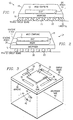
- FIGURE 3 is a perspective view of one embodiment of a copper plate expansion buffer insert between a semiconductor chip and interposer tape.
- a chip 30 can be attached to a copper plate 32 which operates as an expansion buffer insert.
- Copper plate 32 can include bond wire cut-outs 34 that provide openings for bond wires 36 to pass from chip 30 to contacts below copper plate 32.
- An electrically isolating adhesive layer 38 is coupled to copper plate 32 and provides a means for attaching copper plate 32 to interposer tape 40.
- Interposer tape 40 can include copper traces 42 that provide electrical connections from bond wires 36 to solder balls 44 that are positioned on the underside of interposer tape 40. It should be understood that a typical interposer tape 40 would include numerous traces 42 and solder balls 44.
- Copper plate 32 provides thermal cycling performance improvement for the ball grid array package. By matching copper plate 32 with the printed circuit board to produce similar thermal expansion above and below solder balls 44, the stress on solder balls 44 can be reduced without the need for underfill. Of course, copper plate 32 or other expansion buffer insert can produce additional stress on chip 30. However, chip 30, like most semiconductors (e.g., silicon), can be stressed numerous times without damage because chip 30 does not suffer from fatigue as do solder balls 44. Thus, the use of an expansion buffer insert such as copper plate 32 removes the need for underfill by better matching the thermal expansion of the printed circuit board.
- FIGURE 4 is a cross-sectional view of interposer tape 40 of FIGURE 3.
- interposer tape 40 provides a structure for copper traces 42 and solder balls 44. After attaching interposer tape 40 to insert 32, connections can then be made between bond wires 36 and traces 42, thus connecting chip 30 to the printed circuit board through solder balls 44.
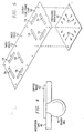
- FIGURE 5 is a perspective view of one embodiment of a copper lead frame strip and a singulated interposer for use in manufacturing ball grid array packages.
- a copper lead frame strip 50 can include index holes 52 defining separate copper plate expansion buffer inserts.
- Each copper plate insert has a plurality of associated bond wire cut-outs 54 similar to those shown in FIGURE 3.
- a singulated interposer 56 can be attached to copper lead frame strip 50 to form a base component for packaging semiconductor chips.
- Singulated interposer 56 can have copper traces 58 that receive bond wire connections through bond wire cut-outs 54. Traces 58 connect to associated solder balls on the underside of singulated interposer 56. Once singulated interposers 56 are attached to each copper plate insert, the combination can be used with existing manufacturing equipment to manufacture ball grid array packages.
- interposer 56 can be provided in a lead frame strip.
- the expansion buffer inserts may be singulated.
- both the expansion buffer inserts and interposers 56 can be provided in lead frame strips that are attached together. This can allow traditional mount, bond and mold equipment to be used to manufacture ball grid array packages with expansion buffer inserts.
Abstract
Description
- This invention relates in general to the field of semiconductor chip packaging, and more particularly to a ball grid array package.
- Ball grid array packages (e.g., the µStar BGA package available from TEXAS INSTRUMENTS) are near chip sized packages for packaging semiconductor chips. Conventionally ball grid array packages are provided with underfill when the package is attached to a printed circuit board in order to improve solder ball lifetimes. The need for underfill arises from the fact that the effective expansion of the package is closer to that of the semiconductor chip (e.g., silicon) than that of the printed circuit board. As a result, without the underfill to alleviate the stress, high solder stress would occur, and the solder balls would eventually fail after repeatedly being stressed. However, the underfill adds a time consuming step to the manufacturing process and limits reworkability.
- Particular and preferred aspects of the invention are set out in the accompanying independent and dependent claims. Features of the dependent claims may be combined with those of the independent claims as appropriate and in combinations other than those explicitly set out in the claims.
- In accordance with the present invention, a ball grip array package having an expansion buffer insert and a method of construction are provided. Through the provision of an expansion buffer insert it is possible to avoid having to use underfill in the package.
- According to one aspect of the present invention, the ball grid array package includes an interposer having traces on a first surface and associated solder balls on an opposite surface. An expansion buffer insert is provided and has bond wire openings and is coupled to the first surface of the interposer. A semiconductor chip is coupled to an opposite surface of the expansion buffer insert and is connected to the traces via bond wires. The package then has a mold compound encasing the semiconductor chip and the expansion buffer insert. In one embodiment the expansion buffer insert is a copper plate.
- According to another aspect of the present invention, a method is provided for manufacturing a ball grid array package. An expansion buffer insert is attached to a first surface of all interposer, where the expansion buffer insert has bond wire openings and the interposer has traces on the first surface and associated solder balls on an opposite surface. A semiconductor chip is attached to an opposite surface of the expansion buffer insert and connected to the traces via bond wires. The semiconductor chip and the expansion buffer insert are then encased in a mold compound. In certain embodiments, the expansion buffer insert and interposer can be singulated (formed as a single unit) or can be formed as one of many on a strip.
- It is thus possible to eliminate the need for underfill by reducing the stress on solder balls through the addition of an embedded expansion buffer insert (e.g., a copper plate) between the semiconductor chip and the interposer in a ball grid array package.
- The expansion buffer insert may advantageously have a thickness that is similar to a standard lead frame thickness, in which case the expansion buffer insert can form a part of a lead frame complete with index holes and to which the interposer can be attached. Thus, traditional mount, bond and mold equipment can be used to manufacture the ball grid array package with the expansion buffer insert. Also, interposer material usage is minimized.
- The expansion buffer insert may advantageously have a high thermal conductivity to provide improved thermal performance resulting from the good heat spreading abilities of the expansion buffer insert.
- Further technical advantages should be apparent from the drawings, description and claims.
- A more complete understanding of the present invention and advantages thereof may be acquired by referring to the following description taken in conjunction with the accompanying drawing, in which like reference numbers indicate like features, and wherein:
- FIGURE 1 is a cross-sectional view of a conventional ball grid array package attached to a printed circuit board and having underfill;
- FIGURE 2 is a cross-sectional view of one embodiment of a ball grid array package attached to a printed circuit board and having an expansion buffer insert;
- FIGURE 3 is a perspective view of one embodiment of a copper plate expansion buffer insert between a semiconductor chip and interposer tape;
- FIGURE 4 is a cross-section of the interposer tape of FIGURE 3; and
- FIGURE 5 is a perspective view of one embodiment of a copper lead frame strip and a singulated interposer for use in manufacturing ball grid array packages.
-
- FIGURE 1 is a cross-sectional view of a conventional ball grid array package, indicated generally at 10, attached to a printed circuit board and having underfill. As shown,
package 10 includes asemiconductor chip 12 having a die attach layer 14 (e.g., adhesive) that connectschip 12 to aninterposer 16. Amold compound 18 encaseschip 12 and dieattach 14 to protectchip 12 from the external environment. A plurality of solder balls are coupled to interposer 16 and provide connections to a printed circuit board, as shown.Underfill 22 is provided betweeninterposer 16 and the printed circuit board and is formed from a material that reduces the effect of thermal expansion. The purpose ofunderfill 22 is to alleviate stress onsolder balls 20 due to thermal expansion mismatch betweenpackage 10 and the printed circuit board and thereby extend the lifetime ofsolder balls 20. As mentioned above, the process of addingunderfill 22 is time-consuming and is performed afterpackage 10 has been mounted on the printed circuit board. - FIGURE 2 is a cross-sectional view of one embodiment of a ball grid array package, indicated generally at 24, attached to a printed circuit board and having an expansion buffer insert. As shown,
package 24 is similar topackage 10 of FIGURE 1. Anexpansion buffer insert 26 is positioned betweenchip 12 andinterposer 16 and is attached to interposer 16 by an electrically isolatingadhesive attach 28. Insert 26 can be constructed from copper or other material to provide a thermal expansion more similar to that of the printed circuit board. - In general, the thermal cycling performance of ball
grid array package 24 is a strong function of the printed circuit board material in thickness. By inserting expansion buffer insert 26 (such as a copper plate) underchip 12, the strain onsolder balls 20 can be reduced (e.g., 3%) for the same thermal conditions.Chip 12 may then experience a higher stress (e.g., 10% more). However,chip 12 can withstand such stress without damage or fatigue. Consequently,insert 26 reduces the stress on and extends the lifetime ofsolder balls 20 without the need forunderfill 22 and without degrading performance ofchip 12. - FIGURE 3 is a perspective view of one embodiment of a copper plate expansion buffer insert between a semiconductor chip and interposer tape. As shown, a
chip 30 can be attached to acopper plate 32 which operates as an expansion buffer insert.Copper plate 32 can include bond wire cut-outs 34 that provide openings forbond wires 36 to pass fromchip 30 to contacts belowcopper plate 32. An electrically isolatingadhesive layer 38 is coupled tocopper plate 32 and provides a means for attachingcopper plate 32 to interposertape 40.Interposer tape 40 can includecopper traces 42 that provide electrical connections frombond wires 36 tosolder balls 44 that are positioned on the underside ofinterposer tape 40. It should be understood that atypical interposer tape 40 would includenumerous traces 42 andsolder balls 44. -
Copper plate 32 provides thermal cycling performance improvement for the ball grid array package. By matchingcopper plate 32 with the printed circuit board to produce similar thermal expansion above and belowsolder balls 44, the stress onsolder balls 44 can be reduced without the need for underfill. Of course,copper plate 32 or other expansion buffer insert can produce additional stress onchip 30. However,chip 30, like most semiconductors (e.g., silicon), can be stressed numerous times without damage becausechip 30 does not suffer from fatigue as dosolder balls 44. Thus, the use of an expansion buffer insert such ascopper plate 32 removes the need for underfill by better matching the thermal expansion of the printed circuit board. - FIGURE 4 is a cross-sectional view of
interposer tape 40 of FIGURE 3. As shown,interposer tape 40 provides a structure forcopper traces 42 andsolder balls 44. After attachinginterposer tape 40 to insert 32, connections can then be made betweenbond wires 36 and traces 42, thus connectingchip 30 to the printed circuit board throughsolder balls 44. - FIGURE 5 is a perspective view of one embodiment of a copper lead frame strip and a singulated interposer for use in manufacturing ball grid array packages. As shown, a copper lead frame strip 50 can include
index holes 52 defining separate copper plate expansion buffer inserts. Each copper plate insert has a plurality of associated bond wire cut-outs 54 similar to those shown in FIGURE 3. Asingulated interposer 56 can be attached to copper lead frame strip 50 to form a base component for packaging semiconductor chips.Singulated interposer 56 can have copper traces 58 that receive bond wire connections through bond wire cut-outs 54.Traces 58 connect to associated solder balls on the underside ofsingulated interposer 56. Oncesingulated interposers 56 are attached to each copper plate insert, the combination can be used with existing manufacturing equipment to manufacture ball grid array packages. - In alternate embodiments,
interposer 56 can be provided in a lead frame strip. The expansion buffer inserts may be singulated. Further, both the expansion buffer inserts andinterposers 56 can be provided in lead frame strips that are attached together. This can allow traditional mount, bond and mold equipment to be used to manufacture ball grid array packages with expansion buffer inserts. - Although the present invention has been described in detail, it should be understood that various changes, substitutions and alterations can be made thereto without departing from the spirit and scope of the invention.
Claims (14)
- A ball grid array package, comprising:an interposer having traces on a first surface and associated solder balls on an opposite surface;an expansion buffer insert having bond wire openings, the expansion buffer insert having a first surface coupled to the first surface of the interposer;a semiconductor chip coupled to an opposite surface of the expansion buffer insert, the semiconductor chip connected to the traces via bond wires; anda mold compound encasing the semiconductor chip and the expansion buffer insert.
- A method of manufacturing a ball grid array package, comprising:attaching a first surface of an expansion buffer insert to a first surface of an interposer, where the expansion buffer insert has bond wire openings, and where the interposer has traces on the first surface and associated solder balls on an opposite surface of the interposer;attaching a semiconductor chip to an opposite surface of the expansion buffer insert;connecting the semiconductor chip to the traces via bond wires; andencasing the semiconductor chip and the expansion buffer insert in a mold compound.
- The package of claim 1 or the method of claim 2, wherein the expansion buffer insert is one of a plurality of expansion buffer inserts.
- The package or method of claim 3, wherein the expansion buffer inserts are formed in a lead frame strip.
- The package or method of claim 4, wherein the lead frame strip is a copper lead frame strip.
- The package of claim 1 or the method of claim 2, wherein the expansion buffer insert is a singulated insert.
- The package or method of any one of the preceding claims, wherein the interposer is a singulated interposer.
- The package or method of any one of claims 1 to 6, wherein the interposer is one of a plurality of interposers.
- The package or method of claim 8, wherein the plurality of interposers are formed in the, a or a further lead frame strip.
- The package or method of any one of the preceding claims, wherein the expansion buffer insert is a copper plate.
- The package or method of any one of the preceding claims, wherein the bond wire openings are formed by cut-outs in the or each expansion buffer insert.
- The package or method of any one of the preceding claims, wherein the traces are copper traces.
- The package or method of any one of the preceding claims, wherein the expansion buffer insert is coupled to the interposer by an adhesive attach layer, preferably by an electrically isolating adhesive attach layer.
- The package or method of any one of the preceding claims, wherein the semiconductor chip is attached to the expansion buffer insert by an adhesive attach layer.
Applications Claiming Priority (2)
| Application Number | Priority Date | Filing Date | Title |
|---|---|---|---|
| US6832897P | 1997-12-19 | 1997-12-19 | |
| US68328P | 1997-12-19 |
Publications (2)
| Publication Number | Publication Date |
|---|---|
| EP0926730A2 true EP0926730A2 (en) | 1999-06-30 |
| EP0926730A3 EP0926730A3 (en) | 2001-03-21 |
Family
ID=22081859
Family Applications (1)
| Application Number | Title | Priority Date | Filing Date |
|---|---|---|---|
| EP98310316A Withdrawn EP0926730A3 (en) | 1997-12-19 | 1998-12-16 | Ball grid array package and method of construction thereof |
Country Status (4)
| Country | Link |
|---|---|
| EP (1) | EP0926730A3 (en) |
| JP (1) | JPH11243162A (en) |
| KR (1) | KR19990063228A (en) |
| TW (1) | TW436940B (en) |
Cited By (1)
| Publication number | Priority date | Publication date | Assignee | Title |
|---|---|---|---|---|
| EP4231344A3 (en) * | 2022-01-28 | 2023-11-01 | InnoLux Corporation | Electronic device |
Families Citing this family (2)
| Publication number | Priority date | Publication date | Assignee | Title |
|---|---|---|---|---|
| JP2002026198A (en) | 2000-07-04 | 2002-01-25 | Nec Corp | Semiconductor device and manufacturing method therefor |
| US8614491B2 (en) * | 2009-04-07 | 2013-12-24 | Honeywell International Inc. | Package interface plate for package isolation structures |
Citations (2)
| Publication number | Priority date | Publication date | Assignee | Title |
|---|---|---|---|---|
| US5241133A (en) * | 1990-12-21 | 1993-08-31 | Motorola, Inc. | Leadless pad array chip carrier |
| US5598321A (en) * | 1995-09-11 | 1997-01-28 | National Semiconductor Corporation | Ball grid array with heat sink |
-
1998
- 1998-12-16 EP EP98310316A patent/EP0926730A3/en not_active Withdrawn
- 1998-12-18 KR KR1019980056324A patent/KR19990063228A/en not_active Application Discontinuation
- 1998-12-21 JP JP10361746A patent/JPH11243162A/en active Pending
- 1998-12-23 TW TW087121116A patent/TW436940B/en not_active IP Right Cessation
Patent Citations (2)
| Publication number | Priority date | Publication date | Assignee | Title |
|---|---|---|---|---|
| US5241133A (en) * | 1990-12-21 | 1993-08-31 | Motorola, Inc. | Leadless pad array chip carrier |
| US5598321A (en) * | 1995-09-11 | 1997-01-28 | National Semiconductor Corporation | Ball grid array with heat sink |
Cited By (1)
| Publication number | Priority date | Publication date | Assignee | Title |
|---|---|---|---|---|
| EP4231344A3 (en) * | 2022-01-28 | 2023-11-01 | InnoLux Corporation | Electronic device |
Also Published As
| Publication number | Publication date |
|---|---|
| TW436940B (en) | 2001-05-28 |
| JPH11243162A (en) | 1999-09-07 |
| KR19990063228A (en) | 1999-07-26 |
| EP0926730A3 (en) | 2001-03-21 |
Similar Documents
| Publication | Publication Date | Title |
|---|---|---|
| US6101100A (en) | Multi-electronic device package | |
| US7342305B1 (en) | Thermally enhanced cavity-down integrated circuit package | |
| US7656015B2 (en) | Packaging substrate having heat-dissipating structure | |
| US6201300B1 (en) | Printed circuit board with thermal conductive structure | |
| US6815251B1 (en) | High density modularity for IC's | |
| US6873043B2 (en) | Electronic assembly having electrically-isolated heat-conductive structure | |
| US5157480A (en) | Semiconductor device having dual electrical contact sites | |
| US6734552B2 (en) | Enhanced thermal dissipation integrated circuit package | |
| US6449159B1 (en) | Semiconductor module with imbedded heat spreader | |
| US5866949A (en) | Chip scale ball grid array for integrated circuit packaging | |
| EP0638931B1 (en) | Multi-chip module | |
| US7786593B2 (en) | Integrated circuit die with pedestal | |
| US20030209791A1 (en) | Semiconductor structure having stacked semiconductor devices | |
| US20040021477A1 (en) | Method for ball grid array chip packages having improved testing and stacking characteristics | |
| US20070138625A1 (en) | Semiconductor package with heat dissipating structure and method of manufacturing the same | |
| JP2006501677A (en) | Heat resistant package for block molded assemblies | |
| CA2306475A1 (en) | Method and construction for thermally enhancing a microelectronic package | |
| EP0977253A3 (en) | Flip-chip bonding of semiconductor chips | |
| US5243497A (en) | Chip on board assembly | |
| US6032355A (en) | Method of forming thermal conductive structure on printed circuit board | |
| US6320136B1 (en) | Layered printed-circuit-board and module using the same | |
| EP0926730A2 (en) | Ball grid array package and method of construction thereof | |
| US20020041039A1 (en) | Semiconductor device without use of chip carrier and method for making the same | |
| US6879050B2 (en) | Packaged microelectronic devices and methods for packaging microelectronic devices | |
| US7629682B2 (en) | Wafer level package configured to compensate size difference in different types of packages |
Legal Events
| Date | Code | Title | Description |
|---|---|---|---|
| PUAI | Public reference made under article 153(3) epc to a published international application that has entered the european phase |
Free format text: ORIGINAL CODE: 0009012 |
|
| AK | Designated contracting states |
Kind code of ref document: A2 Designated state(s): AT BE CH CY DE DK ES FI FR GB GR IE IT LI LU MC NL PT SE |
|
| AX | Request for extension of the european patent |
Free format text: AL;LT;LV;MK;RO;SI |
|
| PUAL | Search report despatched |
Free format text: ORIGINAL CODE: 0009013 |
|
| AK | Designated contracting states |
Kind code of ref document: A3 Designated state(s): AT BE CH CY DE DK ES FI FR GB GR IE IT LI LU MC NL PT SE |
|
| AX | Request for extension of the european patent |
Free format text: AL;LT;LV;MK;RO;SI |
|
| AKX | Designation fees paid | ||
| REG | Reference to a national code |
Ref country code: DE Ref legal event code: 8566 |
|
| STAA | Information on the status of an ep patent application or granted ep patent |
Free format text: STATUS: THE APPLICATION IS DEEMED TO BE WITHDRAWN |
|
| 18D | Application deemed to be withdrawn |
Effective date: 20010922 |