EP0924766A2 - Memory cell array, method of its manufacture and method of its use - Google Patents
Memory cell array, method of its manufacture and method of its use Download PDFInfo
- Publication number
- EP0924766A2 EP0924766A2 EP98120336A EP98120336A EP0924766A2 EP 0924766 A2 EP0924766 A2 EP 0924766A2 EP 98120336 A EP98120336 A EP 98120336A EP 98120336 A EP98120336 A EP 98120336A EP 0924766 A2 EP0924766 A2 EP 0924766A2
- Authority
- EP
- European Patent Office
- Prior art keywords
- word line
- trenches
- selection transistor
- memory cell
- memory cells
- Prior art date
- Legal status (The legal status is an assumption and is not a legal conclusion. Google has not performed a legal analysis and makes no representation as to the accuracy of the status listed.)
- Granted
Links
Images


Classifications
-
- H—ELECTRICITY
- H10—SEMICONDUCTOR DEVICES; ELECTRIC SOLID-STATE DEVICES NOT OTHERWISE PROVIDED FOR
- H10B—ELECTRONIC MEMORY DEVICES
- H10B12/00—Dynamic random access memory [DRAM] devices
-
- H—ELECTRICITY
- H10—SEMICONDUCTOR DEVICES; ELECTRIC SOLID-STATE DEVICES NOT OTHERWISE PROVIDED FOR
- H10B—ELECTRONIC MEMORY DEVICES
- H10B53/00—Ferroelectric RAM [FeRAM] devices comprising ferroelectric memory capacitors
- H10B53/30—Ferroelectric RAM [FeRAM] devices comprising ferroelectric memory capacitors characterised by the memory core region
-
- H—ELECTRICITY
- H10—SEMICONDUCTOR DEVICES; ELECTRIC SOLID-STATE DEVICES NOT OTHERWISE PROVIDED FOR
- H10B—ELECTRONIC MEMORY DEVICES
- H10B12/00—Dynamic random access memory [DRAM] devices
- H10B12/01—Manufacture or treatment
- H10B12/02—Manufacture or treatment for one transistor one-capacitor [1T-1C] memory cells
- H10B12/05—Making the transistor
- H10B12/053—Making the transistor the transistor being at least partially in a trench in the substrate
-
- H—ELECTRICITY
- H10—SEMICONDUCTOR DEVICES; ELECTRIC SOLID-STATE DEVICES NOT OTHERWISE PROVIDED FOR
- H10B—ELECTRONIC MEMORY DEVICES
- H10B12/00—Dynamic random access memory [DRAM] devices
- H10B12/30—DRAM devices comprising one-transistor - one-capacitor [1T-1C] memory cells
- H10B12/34—DRAM devices comprising one-transistor - one-capacitor [1T-1C] memory cells the transistor being at least partially in a trench in the substrate
-
- H—ELECTRICITY
- H10—SEMICONDUCTOR DEVICES; ELECTRIC SOLID-STATE DEVICES NOT OTHERWISE PROVIDED FOR
- H10B—ELECTRONIC MEMORY DEVICES
- H10B53/00—Ferroelectric RAM [FeRAM] devices comprising ferroelectric memory capacitors
-
- H—ELECTRICITY
- H10—SEMICONDUCTOR DEVICES; ELECTRIC SOLID-STATE DEVICES NOT OTHERWISE PROVIDED FOR
- H10B—ELECTRONIC MEMORY DEVICES
- H10B69/00—Erasable-and-programmable ROM [EPROM] devices not provided for in groups H10B41/00 - H10B63/00, e.g. ultraviolet erasable-and-programmable ROM [UVEPROM] devices
Definitions
- Memory cell arrangements in particular DRAM arrangements, ROM arrangements, EPROM arrangements and EEPROM arrangements, have a large number of memory cells, most of them matrix-shaped are arranged.
- the individual memory cells are each can be controlled via a bit line and a word line.
- the memory cells each have a memory element where information is stored.
- the storage The information takes place, for example, via a storage capacity stored charge, via a floating on a Gate stored charge, or through properties of a Transistor, for example the threshold voltage, or over the presence or absence of a manager Connection to the bit line.
- the individual memory cells are used to read out the information sequentially over the associated word line and bit line controlled and the information by voltage or Current evaluation read out (see for example Y. Nakagome et al, IEEE Journal of Solid-State Circuits, Vol. 26, No. 4, 1991, pages 465 to 470).
- the current rating is regarding to prefer reading speed to voltage evaluation, however, it requires increased circuitry.
- For Accelerating the reading process is often several to Example 256 memory cells combined into a cell block. The individual cell blocks are then read out in parallel. The reading process takes place in the individual cell block however, still sequential.
- Example DRAM devices or EEPROM devices becomes Writing information into the respective memory cell also via the associated bit line and the word line controlled.
- the bit line is at a voltage level applied to the information to be registered corresponds.
- the information is written in sequentially in all memory cells.
- the bit line each time from one state of tension to another state of tension be reloaded. This is electrical with a consumption Performance related, especially when deployed the memory cell arrangement in mobile devices such as Mobile phones, notebook computers, database computers or PDA (Personal Digital Assistant) is perceived as disturbing.
- PDA Personal Digital Assistant
- a DRAM cell arrangement is known from DE 19 519 160 C1, which can be produced with a memory cell area of 4F 2 , where F is the minimum structure size that can be produced in the respective technology.
- a vertical MOS transistor is provided per memory cell, the first source / drain region of which is connected to a storage node of a storage capacitor, the channel region of which is surrounded by a gate electrode and the second source / drain region of which is connected to a buried bit line .
- the gate electrodes of vertical MOS transistors adjacent along a word line adjoin one another and together form the word line.
- the invention is based on the problem of a memory cell arrangement specify which can be controlled in an improved manner is.
- the memory cell arrangement should have a Storage density can be produced, as in the Giga-Bit generations is required.
- a manufacturing process is also intended and an operating method for such a memory cell arrangement can be specified.
- the memory cells each have at least one one with respect to a main surface of the semiconductor substrate vertical selection transistor on that with a memory element connected is.
- the selection transistor is preferably connected between a bit line and the memory element.
- the bit lines can also be connected differently.
- the memory cells are each via a first word line and a second word line can be driven, the first Cross the word line and the second word line.
- the control a memory cell takes place only via the first word line and the second word line. This allows bit lines can be read out in parallel.
- the memory cells are likewise each driven via the first word line and the second word line.
- the bit line is only used to apply the voltage level corresponding to the information and not for control. Therefore, in order to write information corresponding to a predetermined voltage level, all of the bit lines can be supplied with the predetermined voltage level.
- the memory cells in which the associated information is to be stored are controlled via the first word lines and the second word lines. This is written into all corresponding memory cells in one cycle. Two processes are therefore sufficient for writing in digital information: first, writing one in parallel One "and second parallel registration of one Zero ". This speeds up the writing process considerably in comparison with the prior art.
- the bit line only has to be reloaded as often as the number of different items of information. In the case of digital information, the bit line only has to be reloaded twice the power consumption is reduced.
- this is also used for refreshing the information (refresh) exploited.
- the stored information via a shift register read out.
- the data word stored in the shift register is subsequently used to control the first word lines and of the second word lines, the bit line being on the respective voltage level is set.
- Bit line Due to the essential compared to the prior art lower number of required reloading operations Bit line is the power consumption when registered as well significantly reduced when refreshing information.
- a monocrystalline is used as the semiconductor substrate Silicon wafer or the monocrystalline silicon layer one Suitable SOI substrate.
- the memory cell arrangement is designed as a DRAM arrangement.
- the memory element is preferably configured as a storage capacitance, which can be implemented both in the semiconductor substrate, in particular as a trench capacitor, and on the main surface of the semiconductor substrate or above the main surface of the semiconductor substrate, in particular as a stacked capacitor.
- the usual storage dielectrics are suitable as the capacitor dielectric, in particular silicon oxide, combinations of silicon oxide and silicon nitride or high-epsilon dielectrics such as, for example, BST (barium strontium titanate), Ta 2 O 5 or SBT (strontium bismuth tantalate).
- the Memory cells each cell block are with a common bit line connected. This has the advantage that the bit line resistance is reduced. It also results from this new freedom for the design of the sense amplifier.
- the memory cells each a first selection transistor and a second selection transistor have that in series between the bit line and the storage element are switched.
- the first selection transistor from the first word line and the second selection transistor can be driven by the second word line.
- neighboring memory cells each have a common one first selection transistor and a common first word line exhibit.
- the neighboring memory cells have different ones second selection transistors and different second word lines. They are then shared over each first word line and the different second Word lines can be controlled.
- two are adjacent Memory cells with a common first selection transistor and different second selection transistors in one Semiconductor column arranged.
- the semiconductor column borders on the Main surface of the semiconductor substrate and has flanks, that cross the main surface of the semiconductor substrate. she will in particular by essentially parallel first ones Trenches and essentially parallel second trenches, that cross each other, defined.
- the common first selection transistor is designed as a vertical MOS transistor, whose gate electrode on at least one edge of the semiconductor column is arranged. In the area of the main area are the second selection transistors of the two adjacent memory cells arranged as planar MOS transistors.
- the gate electrodes the second selection transistors are located above the main surface of the semiconductor column. They are part of it of the different second word lines.
- the Is the gate electrode of the common first selection transistor Part of the first word line.
- the neighboring memory cells are arranged in a semiconductor column.
- first gate electrode of the common first selection transistor it is advantageous to be ring-shaped so that it surrounds the semiconductor column.
- the semiconductor columns are from along one of the first Word lines arranged adjacent pairs of memory cells so that their distance is less than the thickness of the first Gate electrodes parallel to the main surface, so limit the first Gate electrodes of adjacent semiconductor columns together and thus form the first word line.
- Cross to The first word line is the distance between adjacent semiconductor columns greater than twice the thickness of the first gate electrodes parallel to the main surface.
- the first word line can be in this case through self-adjusting process steps, the means making without using masks to be adjusted.
- the first selection transistor and along the second selection transistor to arrange at least one flank of a semiconductor column, the adjacent to the main surface of the semiconductor substrate and the the main surface has intersecting flanks.
- the first selection transistor and the second selection transistor are included arranged one above the other.
- a first gate electrode of the first Selection transistor and a second gate electrode of the second Selection transistors border on the respective edge of the Semiconductor column.
- the first gate electrode and the second gate electrode die Semiconductor column surrounds each ring.
- this configuration is produced in that in the main area of the semiconductor substrate first trenches and second trenches be etched.
- the first trenches run one below the other essentially parallel.
- the second trenches run also essentially parallel to each other.
- the first Trenches and the second trenches cross each other.
- Two neighboring ones first trenches and second trenches define one of the semiconductor columns.
- the cross section of the semiconductor columns enlarged at least one auxiliary structure so that the distance adjacent semiconductor columns in the direction of the first word lines less than in the direction of the second word lines is.
- each semiconductor column has a memory cell.
- the memory cells each have only one selection transistor which can be controlled via the first word line and the second word line.
- the selection transistor is implemented in particular as a MOS transistor, which has two gate electrodes between the source and drain region, which are part of the first word line and part of the second word line. This takes advantage of the fact that the stray field of the first word line and the stray field of the second word line overlap, so that a continuous conductive channel can be switched on by actuation via the first word line and the second word line.
- the selection transistor is advantageous to arrange the selection transistor on the flanks of a semiconductor column, which is delimited by adjacent first trenches and second trenches that intersect, and to arrange the first word line and the second word line on flanks of the semiconductor column one above the other . If the width and the mutual spacing of the first trenches and the second trenches each have a minimally producible structure size F, the memory cell arrangement can be realized with an area requirement of 4F 2 per memory cell.
- the semiconductor columns can both by etching the trenches in a semiconductor substrate as well as by selective epitaxy inside openings of a lattice-shaped insulation structure be formed.
- the grid-like insulation structure defines in the second case, the course of the trenches.
- each memory cell has the first and second word lines is controllable, the memory cell arrangement by appropriate control of the first and second word lines operate in the sense of a folded bitline architecture.
- a semiconductor substrate which has monocrystalline silicon at least in the region of a main surface 11 comprises a p-doped substrate body 12, an n + -doped silicon layer 13 arranged thereon, a first p-doped layer 14 arranged thereon and a second p-doped silicon layer arranged thereon 15 (see Figure 1).
- the p-doped substrate body 12 has a dopant concentration of 10 16 cm -3 .
- the n + -doped silicon layer 13 is produced by epitaxial growth in a thickness of 500 nm. It has a dopant concentration of 10 20 cm -3 .
- the first p-doped silicon layer 14 and the second p-doped silicon layer 15 have grown epitaxially and together have a thickness of 500 nm.
- the first p-doped silicon layer 14 has a thickness of 200 nm and a dopant concentration of 10 17 cm -3 .
- the second p-doped silicon layer 15 has a thickness of 300 nm and a dopant concentration of 10 16 cm -3 .
- a first trench mask 16 is then formed on the main surface 11 by depositing and structuring an SiO 2 layer.
- the SiO 2 layer is deposited in a TEOS process in a layer thickness of 150 nm and structured with the help of a photoresist mask by dry etching with CHF 3 , O 2 .
- the first trench mask 16 has strip-shaped openings which have a width of 250 nm and a mutual spacing of 250 nm. The width and the distance each correspond to a structure size F that can be minimally produced in the technology used.
- first trenches 17 are etched, the first trench mask 16 being used as an etching mask in a dry etching process with HBr, He, O 2 , NF 3 .
- the first trench mask 16 is then removed by wet chemical means, for example using HF (see FIG. 2).
- the depth of the first trenches 17 is 1100 nm.
- the first trenches 17 thus extend into the p-doped substrate body 12.
- Strip-shaped bit lines 13 ′ are formed from the n + -doped silicon layer 13.
- An SiO 2 layer 18 is subsequently deposited, which completely fills the first trenches 17.
- the SiO 2 layer 18 is deposited in a TEOS process with a layer thickness of 200 nm (see FIG. 3).
- a photoresist mask 19 is formed on the surface of the SiO 2 layer 18 and has strip-shaped openings.
- the strip-shaped openings of the photoresist mask 19 run transversely to the first trenches 17 (see FIG. 3 and FIG. 4).
- the strip-shaped openings in the photoresist mask 19 have a width of 250 nm and a mutual distance of 1250 nm.
- a second trench mask 18 ' is formed from the SiO 2 layer 18 by dry etching with Ar, CF 4 , CHF 3 , N 2 , He.
- the photoresist mask 19 is subsequently removed.
- the first trenches 17 remain filled with SiO 2 .
- SiO 2 spacers 19 are formed on flanks of the second trench mask 18 ′ perpendicular to the main surface 11 (see FIG. 5) .
- second trenches 110 are formed by anisotropic dry etching (see FIG. 5).
- the second trenches 110 are etched to a depth of 500 nm. They extend into the bit lines 13 'without, however, cutting through the bit lines 13'.
- the second trenches 110 must be so deep that the first p-doped silicon layer 14 is reliably severed.
- the width of the second trenches 110 is 90 nm. In comparison to the width of the strip-shaped openings in the second trench mask 18 ', it is reduced by the width of the SiO 2 spacer 190.
- the part of the second trench mask 18 ′ located in the first trenches 17 is etched to such an extent that first isolation structures 18 ′′ are formed from the second trench mask 18 ′ in the trenches 17 (see FIGS. 6 and 7).
- the first insulation structures 18 ′′ cover the bottom of the first trenches and extend into the upper region of the bit lines 13 ′.
- the height of the first insulation structures 18 ′′ is approximately 500 nm.
- a first dielectric layer 111 made of SiO 2 with a layer thickness of 5 nm is formed by thermal oxidation.
- a conductive layer 112 is applied to the first dielectric layer 111.
- the conductive layer 112 is formed from in-situ doped polysilicon in a layer thickness of 80 nm. Phosphorus is used as the dopant.
- the dopant concentration is 10 21 cm -3 .
- the conductive layer 112 completely fills the second trenches 110.
- the first trenches 17 are not filled by the conductive layer 112 (see FIG. 6 and FIG. 7).
- the conductive layer 112 is selectively etched to the first dielectric layer 111 by anisotropic etching with He, HBr, Cl 2 , C 2 F 6 .
- the conductive layer 112 is removed to a depth of 200 nm below the main surface 11.
- First word lines 112 ′ are formed from the conductive layer 112.
- the height of the first word lines 112 ′ is dimensioned such that it reliably covers the area in which the first dielectric layer 111 covers the flanks of the first p-doped silicon layer 14.
- the word line 112 ' is formed from ring-shaped elements which each surround one of the semiconductor columns. Annular elements adjacent in the direction of the first trenches 17 adjoin one another (see FIGS. 8 and 9).
- the first trenches 17 and the second trenches 110 are filled with a second insulation structure 113.
- the SiO 2 layer is deposited in a TEOS process with a layer thickness of 200 nm. The etching back takes place at CHF 3 , O 2 .
- the second insulation structure 113 is formed, the main surface 11 is exposed outside the first trenches 17 and the second trenches 110.
- a second dielectric layer 114 made of SiO 2 with a layer thickness of 5 nm is formed by thermal oxidation.
- Strip-shaped second word lines 115 and strip-shaped silicon nitride structures 116 are produced on the second dielectric layer 114 (see FIGS. 8 and 9).
- the second word lines 115 run parallel to the second trenches 110.
- a second conductive layer and a silicon nitride layer are deposited and structured in the form of a strip using a photoresist mask. The following etching process is used for this: CF 4 , O 2 , N 2 / He, HBr, Cl 2 , C 2 F 6 .
- the second word lines 115 are formed with a width of 250 nm, a distance of 250 nm, a length of 200 ⁇ m and a thickness of 150 nm.
- the second word lines 115 are formed, for example, from polysilicon doped in situ. Phosphorus is suitable as a dopant. The dopant concentration is 10 21 cm -3 .
- the strip-shaped silicon nitride structures 116 have the same dimensions as the second word lines 115 and have a thickness of 50 nm.
- silicon nitride spacers are formed on the flanks of the second word lines.
- the silicon nitride layer is deposited in a CVD process in a layer thickness of 30 nm.
- the etching is done with CF 4 , O 2 , N 2 .
- the etching is selective to SiO 2 .
- first n + -doped regions 118 are subsequently formed.
- the first n + -doped regions 118 are each arranged between adjacent first trenches 17, adjoin the main area 11 and adjoin the interface with the first p-doped silicon layer 14.
- a first n + -doped region 118 is provided in each semiconductor column, which is defined by respectively adjacent first trenches 17 and second trenches 110. It is located approximately in the middle between adjacent second trenches 110 (see FIG. 10 and FIG. 11).
- the first n + -doped regions 118 have a dopant concentration of 10 21 cm -3 and a depth of 300 nm.
- the implantation is carried out with phosphorus or with arsenic.
- a further photoresist mask (not shown) is formed, which is used as an implantation mask to form second n + -doped regions 119.
- Two n + -doped regions 119 are formed in each semiconductor column and are arranged on both sides of the respective first n + -doped region 118 between adjacent second trenches 110.
- the second p-doped silicon layer 15 adjoins the main surface 11 between the second n + -doped region 119 and the first n + -doped region 118.
- the depth of the second n + -doped regions 119 is 100 nm. It is less than the thickness of the second doped silicon layer 15.
- the implantation is carried out with phosphorus.
- One of the second word lines 115 runs between the first n + -doped region 118 and each of the second n + -doped regions 119 on the surface of the semiconductor columns (see FIG. 11).
- An SiO 2 layer 120 is then deposited and planarized by chemical mechanical polishing (CMP). The planar surface of the SiO 2 layer 120 is arranged approximately 500 nm above the main surface 11.
- Contact holes to the second n + -doped regions 119 in the SiO 2 layer 120 are subsequently opened using a photoresist mask and anisotropic etching, for example using Ar, CF 4 , CHF 3 .
- the contact holes are provided with storage nodes 121.
- a doped polysilicon layer is deposited over the entire surface and planarized by chemical-mechanical polishing.
- the storage nodes 121 are doped with phosphorus with a dopant concentration of 10 21 cm -3 in situ.
- the capacitor dielectric 122 is deposited in a layer thickness of 4 nm.
- a capacitor plate 123 made of doped polysilicon is applied to the capacitor dielectric 122.
- the capacitor plate 123 is formed by in situ doped deposition of polysilicon with phosphorus as the dopant and a dopant concentration of 10 21 cm -3 .
- each semiconductor column which is defined by two adjacent first trenches 17 and second trenches 110, comprises two memory cells. These two memory cells have a common first selection transistor, which consists of the bit line 13 ', the first n + -doped region 118 as source / drain regions and the part of the first p-doped silicon layer 14 arranged between them as the channel region, the first gate dielectric 11 'and the first word line 112' is formed.
- Each of the memory cells also has a second selection transistor, each of the first n + -doped region 118 and one of the second n + -doped regions 119 as source / drain regions and the part of the second p-doped silicon layer arranged therebetween 15 as the channel region, the second dielectric layer 114 as the gate dielectric and the second word line 115 arranged above the channel region.
- the two second selection transistors are connected in series with the common first selection transistor via the first n + -doped region 118.
- the second word lines 115 arranged above the second trenches 110 have no electrical function in this memory cell arrangement. Their function is to enable the contact hole etching for the storage nodes 121 selectively with respect to silicon nitride.
- the threshold voltage of the common first selection transistor is about the doping of the first p-doped silicon layer 14 set.
- the threshold voltage of the second selection transistors is about the doping of the second p-doped Silicon layer 15 set.
- the Threshold voltage of the second selection transistors through a special channel implantation can be set.
- the first word lines 112 run across the second Word lines 115 and have annular elements that each surround one of the semiconductor columns (see Figure 12).
- the first trenches 17 are formed with a width of a minimally producible structure size F and a distance of F, and the second trenches 110 with a width of F minus the width of the SiO 2 spacers 190 and a distance between adjacent second trenches 110 of 5F plus the width of the Si0 2 spacer 190, this results in a space requirement of 12F 2 for every two memory cells. This means that the memory cell arrangement can be produced with an area requirement of 6F 2 per memory cell.
- a semiconductor substrate which comprises an SOI substrate 21 onto which a first n + -doped silicon layer 22, a first p-doped silicon layer 23, a second n + -doped silicon layer 24, a second p-doped Silicon layer 25 and a third n + -doped layer 26 are grown epitaxially.
- the third n + -doped layer 26 adjoins a main surface 27 (see FIG. 13).
- the first n + -doped silicon layer 22 is formed in a layer thickness of 300 nm with the dopant As and a dopant concentration of 1 x 10 20 cm -3 .
- the first p-doped silicon layer 23 is formed in a layer thickness of 200 nm with a dopant concentration of 1 x 10 18 cm -3 boron.
- the second n + -doped layer 24 is formed in a layer thickness of 100 nm with a dopant concentration of 1 x 10 19 cm -3 and the dopant As.
- the second p-doped silicon layer 25 is formed in a layer thickness of 200 nm with a dopant concentration of 1 x 10 18 cm -3 with boron.
- the third n + -doped layer 26 is formed in a layer thickness of 200 nm with a dopant concentration of 1 x 10 19 cm -3 with the dopant As.
- a first trench mask 28 is formed on the main surface 27 by depositing and structuring an SiO 2 layer.
- the SiO 2 layer is deposited in a TEOS process with a layer thickness of 150 nm.
- a photoresist mask it is structured by anisotropic etching with CHF 3 , O 2 .
- first trenches 29 are etched.
- the first trenches 29 are produced by anisotropic etching with HBr, He, O 2 , NF 3 .
- the first trenches 29 extend into the first n + -doped silicon layer 22.
- the first trenches 29 are strip-shaped and have a width of 200 nm and a distance between adjacent first trenches 29 of 200 nm.
- the length of the first trenches 29 is 5 ⁇ m and the depth is 800 nm.
- silicon nitride spacers 210 are formed on flanks of the first trenches 29 which are essentially perpendicular to the main surface 27.
- a silicon nitride layer with a thickness of 70 nm is deposited and anisotropically etched with CF 4 , O 2 , N 2 to silicon. The thickness of the nitride layer corresponds to one third of the width of the first trenches 29.
- the space remaining between the silicon spacers 210 is subsequently filled with a first insulation structure 211.
- a first insulation structure 211 For this purpose, an SiO 2 layer is deposited in a TEOS process and anisotropically etched back with CHF 3 , O 2 until the main surface 27 is exposed (see FIG. 14).
- a second trench mask is formed on the main surface 27 by depositing an SiO 2 layer and a silicon nitride layer.
- the SiO 2 layer is deposited in a TEOS process with a thickness of 150 nm.
- the thickness of the silicon nitride layer is 70 nm.
- the nitride layer and the SiO 2 layer are structured by anisotropic etching with CHF 3 , O 2 .
- second trenches 212 are produced. Silicon is first anisotropically etched with HBr, He, O 2 , NF 3 .
- SiO2 is then selectively etched to nitride using C 2 F 6 , C 3 F 8 , the silicon nitride layer of the second trench mask serving as a hard mask. Then the silicon nitride spacer and at the same time the silicon nitride hard mask are removed by wet chemical means using H 3 PO 4 .
- the second trenches 212 run essentially perpendicular to the first trenches 29 (see FIG. 15, in which the section shown by XV-XV in FIG. 14 is shown).
- the second trenches 212 have a strip-shaped cross section with a width of 200 nm, a distance between adjacent second trenches 212 of 200 nm and a length of 5 ⁇ m.
- the depth of the second trenches 212 is 800 nm.
- the second trenches 212 thus also extend into the first n + -doped silicon layer 22.
- the first insulation structure 211 is then removed. This is done selectively by wet chemical etching of silicon oxide to silicon nitride and silicon with HF.
- a first gate oxide 213 with a thickness of 5 nm is formed by thermal oxidation.
- First word lines 214 are subsequently formed by depositing an in-situ doped polysilicon layer and anisotropically etching the doped polysilicon layer.
- the doped polysilicon layer is deposited doped with phosphorus. It has a thickness of 70 nm. This corresponds to a third of the width of the first trenches 29 and the second trenches 212.
- the space between the silicon nitride spacers 210 arranged on opposite flanks of one of the first trenches 29 is thus filled, the second trenches 212, the flanks of which essentially run perpendicular to the main surface 27 are covered with the thin first gate oxide 213, but not.
- the doped polysilicon layer is etched anisotropically with He, HBr, Cl 2 , C 2 F 6 .
- the anisotropic etching is continued until the word lines are at a height in the region of the second n + -doped silicon layer 24.
- the height of the first word lines 214 completely covers the first p-doped silicon layer 23 (see FIG. 16 and FIG. 17).
- Parts of the first word lines 214 each surround one of the Semiconductor columns, each with two adjacent first Trenches 29 and second trenches 212 are defined in an annular manner.
- the space remaining between the silicon nitride spacers 210 in the first trenches 29 is completely with the first word lines 214 filled. In the first trenches 29 therefore delimit ring-shaped elements of the first word lines 214 together.
- the first word lines 214 are thus formed by adjoining annular elements.
- a second insulation structure 215 is formed by deposition of an SiO 2 layer and anisotropic etching back, which fills up the free space remaining between adjacent first word lines 214 in the second trenches 212.
- the height of the second insulation structure 215 is greater than that of the first word lines 214.
- the second insulation structure 215 extends at most to the interface between the second n + -doped silicon layer 24 and the second p-doped silicon layer 25.
- the deposition of the SiO 2 layer takes place in a TEOS process. It is anisotropically etched with Ar, CF 4 , CHF 3 . With this anisotropic etching, first gate oxide located on the main surface 27 and in the upper region of the second trenches 212 is also removed.
- Silicon structures 216 are subsequently grown on exposed silicon surfaces by selective epitaxy.
- the selective epitaxy takes place in the temperature range from 700 ° C to 900 ° C using a process gas containing silane.
- the silicon structures 216 cover the exposed flanks in the region of the second trenches 212 above the second insulation structure 215. Furthermore, they cover the surface of the third n + -doped silicon layer 26.
- the silicon structures 216 have a dimension of 70 nm perpendicular to the silicon surface on which they are located grow up on. This corresponds to a third of the width of the second trenches 212.
- the second trenches 212 are therefore not filled.
- the flanks of the first trenches 29 are covered by the silicon nitride spacers 210, so that no silicon grows on the flanks of the first trenches 29 (see FIG. 18 and FIG. 19).
- Silicon nitride is selectively attacked to silicon by wet chemical etching with H 3 PO 4 . Such an etching exposes the flanks of the third n + -doped silicon layer 26 and the second p-doped silicon layer 25 at least partially. As a result, the height of the silicon nitride spacers 210 in the first trenches 29 is reduced (see FIG. 20).
- a second gate oxide 217 is formed by thermal oxidation exposed silicon areas formed. In particular arises the second gate oxide 217 on the exposed surface of the second p-doped silicon layer 25 in the first trenches 29 (see Figure 20 and Figure 21).
- the second gate oxide 217 is formed in a layer thickness of 5 nm.
- Second word lines 218 are formed by depositing an in-situ doped polysilicon layer and anisotropically etching back the doped polysilicon layer.
- the in-situ doped polysilicon layer is doped with phosphorus and has a dopant concentration of 10 21 cm -3 .
- the doped polysilicon layer is deposited to a thickness of 70 nm. This corresponds to a third of the width of the first trenches 29 and the second trenches 212.
- the anisotropic etching is continued until the flanks of the third n + -doped silicon layer 26 in the region of the first trenches 29 are partially exposed (see FIG. 20).
- the second word lines fill accordingly 218 the second trenches in the distance.
- the second Word lines 218 include annular elements, each surrounded one of the silicon pillars. In the second trenches 212 abut adjacent annular elements so that the second word lines 218 as a chain of adjacent one another annular elements are formed.
- the first trenches 29 are filled with a third insulation structure 219.
- a SiO 2 layer is deposited in a TEOS process and anisotropically etched with CHF 3 , O 2 .
- the third insulation structure 219 is flush with the main surface 27.
- storage nodes 220 arranged on the main surface 27 are formed.
- the storage nodes 220 are formed from the parts of the silicon structure 216 located on the main surface 27.
- the storage nodes 219 are electrically connected to the third n + -doped silicon layer 26.
- a capacitor dielectric 221 is then deposited over the entire surface.
- the capacitor dielectric 221 is formed from SiO 2 , a triple layer of SiO 2 , Si 3 N 4 and SiO 2 or a high-epsilon dielectric, for example BST (barium strontium titanate) or SBT (strontium bismuth tantalate).
- a capacitor plate 222 is applied to the capacitor dielectric 221.
- the capacitor plate 221 is formed by in situ doped deposition of polysilicon in a layer thickness of 200 nm and planarization of the doped polysilicon layer.
- the doped polysilicon layer is doped with phosphorus with a dopant concentration of 10 21 cm -3 (see Figure 22).
- FIG. 23 shows that designated XXIII-XXIII in FIG. 22 Cut.
- FIG. 24 shows that designated XXIV-XXIV in FIG. 22 Cut.
- the first word lines 214 and the second word lines 218 are each ring-shaped as a chain Elements are formed and run parallel to each other.
- the first word lines 214 and the second word lines 218 run across each other.
- each semiconductor column which is defined in each case by two adjacent first trenches 29 and second trenches 212, comprises a memory cell.
- the memory cell has a first selection transistor, which consists of the first n + -doped silicon layer 22 and the second n + -doped silicon layer 24 as source / drain regions, the first p-doped silicon layer 23 as a channel region, the first gate oxide 213 and of the first word line 214 is formed as a gate electrode.
- a second selection transistor of the memory cell is made up of the second n + -doped silicon layer 24 and the third n + -doped silicon layer 26 as a source / drain region, the second p-doped silicon layer 25 as a channel region, the second gate oxide 217 and the second word line 218 formed as a gate electrode.
- the first selection transistor and the second selection transistor are connected in series via the second n + -doped silicon layer 24, which acts as a common source / drain region.
- the first n + -doped silicon layer 22 acts as a common bit line.
- the second n + -doped silicon layer 24 is replaced by a p-doped silicon layer.
- each memory cell comprises only one selection transistor, which, however, is controlled via two gate electrodes which are arranged one above the other and whose stray fields are so large that they overlap.
- the overlapping stray fields when switched on, lead to the formation of a conductive channel from the first n + -doped silicon layer 22 to the third n + -doped silicon layer 26 through all p-doped silicon layers.
- the selection transistor acts like two selection transistors connected in series, since a conductive channel is only formed when both gate electrodes are activated.
Abstract
Description
Speicherzellenanordnungen, insbesondere DRAM-Anordnungen, ROM-Anordnungen, EPROM-Anordnungen und EEPROM-Anordnungen, weisen eine Vielzahl von Speicherzellen auf, die meist matrixförmig angeordnet sind. Die einzelnen Speicherzellen sind dabei jeweils über eine Bitleitung und eine Wortleitung ansteuerbar. Die Speicherzellen weisen jeweils ein Speicherelement auf, in dem Information gespeichert ist. Die Speicherung der Information erfolgt zum Beispiel über eine in einer Speicherkapazität gespeicherte Ladung, über eine auf einem floatenden Gate gespeicherte Ladung, oder über Eigenschaften eines Transistors, zum Beispiel der Einsatzspannung, oder über das Vorhandensein bzw. Nichtvorhandensein einer leitenden Verbindung zur Bitleitung.Memory cell arrangements, in particular DRAM arrangements, ROM arrangements, EPROM arrangements and EEPROM arrangements, have a large number of memory cells, most of them matrix-shaped are arranged. The individual memory cells are each can be controlled via a bit line and a word line. The memory cells each have a memory element where information is stored. The storage The information takes place, for example, via a storage capacity stored charge, via a floating on a Gate stored charge, or through properties of a Transistor, for example the threshold voltage, or over the presence or absence of a manager Connection to the bit line.
Zum Auslesen der Information werden die einzelnen Speicherzellen sequentiell über die zugehörige Wortleitung und Bitleitung angesteuert und die Information durch Spannungs- oder Strombewertung ausgelesen (siehe zum Beispiel Y. Nakagome et al, IEEE Journal of Solid-State Circuits, Vol. 26, Nr. 4, 1991, Seiten 465 bis 470). Die Strombewertung ist bezüglich der Lesegeschwindigkeit der Spannungsbewertung vorzuziehen, sie erfordert jedoch einen erhöhten Schaltungsaufwand. Zur Beschleunigung des Lesevorgangs werden vielfach mehrere, zum Beispiel 256 Speicherzellen zu einem Zellenblock zusammengefaßt. Die einzelnen Zellenblöcke werden dann parallel ausgelesen. Der Auslesevorgang in dem einzelnen Zellenblock erfolgt jedoch nach wie vor sequentiell.The individual memory cells are used to read out the information sequentially over the associated word line and bit line controlled and the information by voltage or Current evaluation read out (see for example Y. Nakagome et al, IEEE Journal of Solid-State Circuits, Vol. 26, No. 4, 1991, pages 465 to 470). The current rating is regarding to prefer reading speed to voltage evaluation, however, it requires increased circuitry. For Accelerating the reading process is often several to Example 256 memory cells combined into a cell block. The individual cell blocks are then read out in parallel. The reading process takes place in the individual cell block however, still sequential.
In elektrisch beschreibbaren Speicherzellenanordnungen, zum Beispiel DRAM-Anordnungen oder EEPROM-Anordnungen, wird zum Einschreiben von Information die jeweilige Speicherzelle ebenfalls über die zugehörige Bitleitung und die Wortleitung angesteuert. Gleichzeitig wird die Bitleitung mit einem Spannungspegel beaufschlagt, der der einzuschreibenden Information entspricht. Das Einschreiben der Information erfolgt sequentiell in alle Speicherzellen. Dabei muß die Bitleitung jedesmal von einem Spannungszustand zum anderen Spannungszustand umgeladen werden. Dieses ist mit einem Verbrauch elektrischer Leistung verbunden, der insbesondere beim Einsatz der Speicherzellenanordnung in mobilen Geräten wie zum Beispiel Mobiltelefone, Notebook-Computer, Datenbankrechner oder PDA (Personal Digital Assistant) als störend empfunden wird.In electrically writable memory cell arrangements, for Example DRAM devices or EEPROM devices, becomes Writing information into the respective memory cell also via the associated bit line and the word line controlled. At the same time, the bit line is at a voltage level applied to the information to be registered corresponds. The information is written in sequentially in all memory cells. The bit line each time from one state of tension to another state of tension be reloaded. This is electrical with a consumption Performance related, especially when deployed the memory cell arrangement in mobile devices such as Mobile phones, notebook computers, database computers or PDA (Personal Digital Assistant) is perceived as disturbing.
Bei DRAM-Anordnungen tritt darüber hinaus das Problem auf, daß die gespeicherte Information in regelmäßigen Zeitabständen wieder aufgefrischt werden muß. Dazu wird die Information zunächst sequentiell aus den Speicherzellen ausgelesen und anschließend wieder eingeschrieben. Auch hier tritt unerwünschter Leistungsverbrauch auf.The problem also arises with DRAM devices, that the stored information at regular intervals needs to be refreshed again. This is the information first read out sequentially from the memory cells and then registered again. Here, too, occurs more undesirably Power consumption on.
Ein weiteres Problem bei DRAM-Anordnungen stellt die von
Speichergeneration zu Speichergeneration zunehmende Speicherdichte
dar. Damit verbunden ist das Erfordernis einer erhöhten
Packungsdichte, das heißt einer Verringerung des Platzbedarfs
pro Speicherzelle. Aus DE 19 519 160 C1 ist eine DRAM-Zellenanordnung
bekannt, die mit einer Speicherzellenfläche
von 4F2 herstellbar ist, wobei F die in der jeweiligen Technologie
minimal herstellbare Strukturgröße ist. Pro Speicherzelle
ist dabei ein vertikaler MOS-Transistor vorgesehen,
dessen erstes Source-/Drain-Gebiet mit einem Speicherknoten
eines Speicherkondensators verbunden ist, dessen Kanalgebiet
ringförmig von einer Gateelektrode umschlossen wird und dessen
zweites Source-/Drain-Gebiet mit einer vergrabenen Bitleitung
verbunden ist. Die Gateelektroden von entlang einer
Wortleitung benachbarten vertikalen MOS-Transistoren grenzen
dabei aneinander und bilden gemeinsam die Wortleitung.Another problem with DRAM arrangements is the increasing memory density from memory generation to memory generation. This is associated with the need for an increased packaging density, that is to say a reduction in the space requirement per memory cell. A DRAM cell arrangement is known from
Der Erfindung liegt das Problem zugrunde, eine Speicherzellenanordnung anzugeben, die auf verbesserte Weise ansteuerbar ist. Insbesondere soll die Speicherzellenanordnung mit einer Speicherdichte herstellbar sein, wie sie in den Giga-Bit-Generationen erforderlich ist. Ferner soll ein Herstellverfahren und ein Betriebsverfahren für eine solche Speicherzellenanordnung angegeben werden.The invention is based on the problem of a memory cell arrangement specify which can be controlled in an improved manner is. In particular, the memory cell arrangement should have a Storage density can be produced, as in the Giga-Bit generations is required. A manufacturing process is also intended and an operating method for such a memory cell arrangement can be specified.
Dieses Problem wird gelöst durch eine Speicherzellenanordnung
gemäß Anspruch 1, ein Verfahren zu deren Herstellung gemäß
Anspruch 12 sowie durch Verfahren zu deren Betrieb gemäß Anspruch
19 und 20. Weitere Ausgestaltungen der Erfindung gehen
aus den abhängigen Ansprüchen hervor.This problem is solved by a memory cell arrangement
according to claim 1, a process for their preparation according to
Es ist ein Halbleitersubstrat mit einer Vielzahl Speicherzellen vorgesehen. Die Speicherzellen weisen jeweils mindestens einen in Bezug auf eine Hauptfläche des Halbleitersubstrats vertikalen Auswahltransistor auf, der mit einem Speicherelement verbunden ist. Vorzugsweise ist der Auswahltransistor zwischen eine Bitleitung und das Speicherelement geschaltet. Die Bitleitungen können jedoch auch anders verschaltet sein. Die Speicherzellen sind jeweils über eine erste Wortleitung und eine zweite Wortleitung ansteuerbar, wobei sich die erste Wortleitung und die zweite Wortleitung kreuzen. Die Ansteuerung einer Speicherzelle erfolgt nur über die erste Wortleitung und die zweite Wortleitung. Dadurch können Bitleitungen parallel ausgelesen werden.It is a semiconductor substrate with a large number of memory cells intended. The memory cells each have at least one one with respect to a main surface of the semiconductor substrate vertical selection transistor on that with a memory element connected is. The selection transistor is preferably connected between a bit line and the memory element. However, the bit lines can also be connected differently. The memory cells are each via a first word line and a second word line can be driven, the first Cross the word line and the second word line. The control a memory cell takes place only via the first word line and the second word line. This allows bit lines can be read out in parallel.
Im Fall einer elektrisch beschreibbaren Speicherzellenanordnung
werden die Speicherzellen ebenfalls jeweils über die erste
Wortleitung und die zweite Wortleitung angesteuert. Die
Bitleitung wird nur zum Anlegen des der Information entsprechenden
Spannungspegels und nicht zur Ansteuerung verwendet.
Daher können zum Einschreiben einer einem vorgegebenen Spannungspegel
entsprechenden Information alle Bitleitungen mit
dem vorgegebenen Spannungspegel beaufschlagt werden. Über die
ersten Wortleitungen und die zweiten Wortleitungen werden
diejenigen Speicherzellen angesteuert, in denen die zugehörige
Information gespeichert werden soll. Diese wird in einem
Takt in alle entsprechenden Speicherzellen eingeschrieben.
Zum Einschreiben einer digitalen Information sind daher zwei
Vorgänge ausreichend: erstens paralleles Einschreiben einer
![]()
![]()
Im Fall einer DRAM-Anordnung wird dieses auch für das Auffrischen der Information (refresh) ausgenutzt. Vorzugsweise wird dabei die gespeicherte Information über ein Schieberegister ausgelesen. Das im Schieberegister gespeicherte Datenwort wird nachfolgend zur Ansteuerung der ersten Wortleitungen und der zweiten Wortleitungen verwendet, wobei die Bitleitung auf die jeweiligen Spannungspegel gelegt wird.In the case of a DRAM arrangement, this is also used for refreshing the information (refresh) exploited. Preferably the stored information via a shift register read out. The data word stored in the shift register is subsequently used to control the first word lines and of the second word lines, the bit line being on the respective voltage level is set.
Bedingt durch die im Vergleich zum Stand der Technik wesentlich geringere Anzahl von erforderlichen Umladevorgängen der Bitleitung wird der Leistungsverbrauch beim Einschreiben sowie beim Auffrischen von Information deutlich verringert.Due to the essential compared to the prior art lower number of required reloading operations Bit line is the power consumption when registered as well significantly reduced when refreshing information.
Als Halbleitersubstrat ist insbesondere eine monokristalline Siliziumscheibe oder die monokristalline Siliziumschicht eines SOI-Substrats geeignet.In particular, a monocrystalline is used as the semiconductor substrate Silicon wafer or the monocrystalline silicon layer one Suitable SOI substrate.
Als Speicherelement sind alle in Speicherzellenanordnungen üblicherweise verwendeten Speicherelemente geeignet. Insbesondere sind Speicherelemente geeignet, die MOS-Transistoren mit unterschiedlichen elektrischen Eigenschaften aufweisen, wie sie vielfach in ROM-Anordnungen verwendet werden, Leitungsunterbrechungen, wie sie in ROM-Anordnungen verwendet werden, Schmelzsicherungen (sogenannten fuses), MOS-Transistoren mit floatendem Gate sowie Speicherkapazitäten geeignet. All are in memory cell arrangements as the memory element Usually used storage elements suitable. Especially memory elements are suitable, the MOS transistors with different electrical properties, as they are often used in ROM arrangements, line breaks, as used in ROM devices be fuses, MOS transistors with floating gate and storage capacities suitable.
Es liegt im Rahmen der Erfindung, die Speicherzellenanordnung als DRAM-Anordnung auszugestalten. In diesem Fall ist sowohl der Vorteil des schnelleren Datenzugriffs beim Lesen und Schreiben von Information als auch der Vorteil des geringeren Leistungsverbrauchs beim Schreiben und Auffrischen der Information nutzbar. In der DRAM-Anordnung ist das Speicherelement vorzugsweise als Speicherkapazität ausgestaltet, die sowohl im Halbleitersubstrat, insbesondere als Grabenkondensator, als auch an der Hauptfläche des Halbleitersubstrats bzw. oberhalb der Hauptfläche des Halbleitersubstrats, insbesondere als Stapelkondensator, realisiert sein kann. Als Kondensatordielektrikum sind die üblichen Speicherdielektrika geeignet, insbesondere Siliziumoxid, Kombinationen aus Siliziumoxid und Siliziumnitrid oder Hochepsilon-Dielektrika wie zum Beispiel BST (Barium-Strontium-Titanat), Ta2O5 oder SBT (Strontium-Wismuth-Tantalat).It is within the scope of the invention to design the memory cell arrangement as a DRAM arrangement. In this case, both the advantage of faster data access when reading and writing information and the advantage of lower power consumption when writing and refreshing the information can be used. In the DRAM arrangement, the memory element is preferably configured as a storage capacitance, which can be implemented both in the semiconductor substrate, in particular as a trench capacitor, and on the main surface of the semiconductor substrate or above the main surface of the semiconductor substrate, in particular as a stacked capacitor. The usual storage dielectrics are suitable as the capacitor dielectric, in particular silicon oxide, combinations of silicon oxide and silicon nitride or high-epsilon dielectrics such as, for example, BST (barium strontium titanate), Ta 2 O 5 or SBT (strontium bismuth tantalate).
Gemäß einer Ausgestaltung der Erfindung werden mehrere der Speicherzellen zu einem Zellenblock zusammengefaßt. Die Speicherzellen jedes Zellenblocks sind mit einer gemeinsamen Bitleitung verbunden. Dieses hat den Vorteil, daß der Bitleitungswiderstand reduziert wird. Ferner ergeben sich dadurch neue Freiheiten für das Design des Leseverstärkers.According to one embodiment of the invention, several of the Memory cells combined into a cell block. The memory cells each cell block are with a common bit line connected. This has the advantage that the bit line resistance is reduced. It also results from this new freedom for the design of the sense amplifier.
Es liegt im Rahmen der Erfindung, daß die Speicherzellen jeweils einen ersten Auswahltransistor und einen zweiten Auswahltransistor aufweisen, die in Reihe zwischen die Bitleitung und das Speicherelement geschaltet sind. Dabei ist der erste Auswahltransistor von der ersten Wortleitung und der zweite Auswahltransistor von der zweiten Wortleitung ansteuerbar. Dabei können im Hinblick auf eine erhöhte Packungsdichte benachbarte Speicherzellen jeweils einen gemeinsamen ersten Auswahltransistor und eine gemeinsame erste Wortleitung aufweisen. Die benachbarten Speicherzellen weisen unterschiedliche zweite Auswahltransistoren und unterschiedliche zweite Wortleitungen auf. Sie sind dann jeweils über die gemeinsame erste Wortleitung und die unterschiedlichen zweiten Wortleitungen ansteuerbar.It is within the scope of the invention that the memory cells each a first selection transistor and a second selection transistor have that in series between the bit line and the storage element are switched. Here is the first selection transistor from the first word line and the second selection transistor can be driven by the second word line. It can with regard to an increased packing density neighboring memory cells each have a common one first selection transistor and a common first word line exhibit. The neighboring memory cells have different ones second selection transistors and different second word lines. They are then shared over each first word line and the different second Word lines can be controlled.
Gemäß einer Ausgestaltung der Erfindung sind zwei benachbarte Speicherzellen mit einem gemeinsamen ersten Auswahltransistor und unterschiedlichen zweiten Auswahltransistoren in einer Halbleitersäule angeordnet. Die Halbleitersäule grenzt an die Hauptfläche des Halbleitersubstrats an und weist Flanken auf, die die Hauptfläche des Halbleitersubstrats kreuzen. Sie wird insbesondere durch im wesentlichen parallel verlaufende erste Gräben und im wesentlich parallel verlaufende zweite Gräben, die einander kreuzen, definiert. Der gemeinsame erste Auswahltransistor ist als vertikaler MOS-Transistor ausgebildet, dessen Gateelektrode an mindestens einer Flanke der Halbleitersäule angeordnet ist. Im Bereich der Hauptfläche sind die zweiten Auswahltransistoren der beiden benachbarten Speicherzellen als planare MOS-Transistoren angeordnet. Die Gateelektroden der zweiten Auswahltransistoren befinden sich jeweils oberhalb der Hauptfläche der Halbleitersäule. Sie sind Bestandteil der unterschiedlichen zweiten Wortleitungen. Die Gateelektrode des gemeinsamen ersten Auswahltransistors ist Bestandteil der ersten Wortleitung. Die benachbarten Speicherzellen sind in einer Halbleitersäule angeordnet.According to one embodiment of the invention, two are adjacent Memory cells with a common first selection transistor and different second selection transistors in one Semiconductor column arranged. The semiconductor column borders on the Main surface of the semiconductor substrate and has flanks, that cross the main surface of the semiconductor substrate. she will in particular by essentially parallel first ones Trenches and essentially parallel second trenches, that cross each other, defined. The common first selection transistor is designed as a vertical MOS transistor, whose gate electrode on at least one edge of the semiconductor column is arranged. In the area of the main area are the second selection transistors of the two adjacent memory cells arranged as planar MOS transistors. The gate electrodes the second selection transistors are located above the main surface of the semiconductor column. They are part of it of the different second word lines. The Is the gate electrode of the common first selection transistor Part of the first word line. The neighboring memory cells are arranged in a semiconductor column.
In dieser Ausgestaltung der Erfindung ist es vorteilhaft, die erste Gateelektrode des gemeinsamen ersten Auswahltransistors ringförmig auszubilden, so daß diese die Halbleitersäule umgibt. Werden die Halbleitersäulen von entlang einer der ersten Wortleitungen benachbarten Speicherzellenpaaren so angeordnet, daß ihr Abstand geringer ist als die Dicke der ersten Gateelektroden parallel zur Hauptfläche, so grenzen die ersten Gateelektroden benachbarter Halbleitersäulen aneinander an und bilden auf diese Weise die erste Wortleitung. Quer zur ersten Wortleitung ist der Abstand benachbarter Halbleitersäulen größer als die doppelte Dicke der ersten Gateelektroden parallel zur Hauptfläche. Die erste Wortleitung läßt sich in diesem Fall durch selbstjustierende Prozeßschritte, das heißt ohne Einsatz von zu justierenden Masken herstellen.In this embodiment of the invention, it is advantageous to first gate electrode of the common first selection transistor to be ring-shaped so that it surrounds the semiconductor column. The semiconductor columns are from along one of the first Word lines arranged adjacent pairs of memory cells so that their distance is less than the thickness of the first Gate electrodes parallel to the main surface, so limit the first Gate electrodes of adjacent semiconductor columns together and thus form the first word line. Cross to The first word line is the distance between adjacent semiconductor columns greater than twice the thickness of the first gate electrodes parallel to the main surface. The first word line can be in this case through self-adjusting process steps, the means making without using masks to be adjusted.
Es liegt ferner im Rahmen der Erfindung, den ersten Auswahltransistor und den zweiten Auswahltransistor jeweils entlang mindestens einer Flanke einer Halbleitersäule anzuordnen, die an die Hauptfläche des Halbleitersubstrats angrenzt und die die Hauptfläche kreuzende Flanken aufweist. Der erste Auswahltransistor und der zweite Auswahltransistor sind dabei übereinander angeordnet. Eine erste Gateelektrode des ersten Auswahltransistors und eine zweite Gateelektrode des zweiten Auswahltransistors grenzen dabei an die jeweilige Flanke der Halbleitersäule an.It is also within the scope of the invention, the first selection transistor and along the second selection transistor to arrange at least one flank of a semiconductor column, the adjacent to the main surface of the semiconductor substrate and the the main surface has intersecting flanks. The first selection transistor and the second selection transistor are included arranged one above the other. A first gate electrode of the first Selection transistor and a second gate electrode of the second Selection transistors border on the respective edge of the Semiconductor column.
Es liegt im Rahmen der Erfindung, daß in dieser Ausgestaltung die erste Gateelektrode und die zweite Gateelektrode die Halbleitersäule jeweils ringförmig umgibt. Vorzugsweise wird diese Ausgestaltung dadurch hergestellt, daß in der Hauptfläche des Halbleitersubstrats erste Gräben und zweite Gräben geätzt werden. Die ersten Gräben verlaufen untereinander jeweils im wesentlichen parallel. Die zweiten Gräben verlaufen untereinander ebenfalls im wesentlichen parallel. Die ersten Gräben und die zweiten Gräben kreuzen einander. Je zwei benachbarte erste Gräben und zweite Gräben definieren dabei eine der Halbleitersäulen. Vor der Herstellung der ersten Gateelektroden wird der Querschnitt der Halbleitersäulen durch mindestens eine Hilfsstruktur vergrößert, so daß der Abstand benachbarter Halbleitersäulen in Richtung der ersten Wortleitungen geringer als in Richtung der zweiten Wortleitungen ist. Im Bereich der zweiten Wortleitungen wird mit Hilfe mindestens einer zweiten Hilfsstruktur der Querschnitt der Halbleitersäulen so vergrößert, daß im Bereich der zweiten Wortleitungen der Abstand zwischen benachbarten Halbleitersäulen in Richtung der zweiten Wortleitungen geringer ist als in Richtung der ersten Wortleitungen. Die ersten Wortleitungen und die zweiten Wortleitungen werden dann selbstjustiert zum Beispiel durch Abscheidung einer Schicht und anisotropes Rückätzen der Schicht im Sinne einer Spacerbildung hergestellt. Da der Abstand benachbarter Halbleitersäulen in der einen Richtung geringer als in der anderen Richtung ist, grenzen benachbarte Gateelektroden in der Richtung mit geringerem Abstand aneinander an, während sie in der Richtung mit dem größeren Abstand voneinander beabstandet sind. Auf diese Weise entstehen kettenartige Leitungen, die parallel zueinander verlaufen. In dieser Ausgestaltung weist jede Halbleitersäule eine Speicherzelle auf.It is within the scope of the invention that in this embodiment the first gate electrode and the second gate electrode die Semiconductor column surrounds each ring. Preferably this configuration is produced in that in the main area of the semiconductor substrate first trenches and second trenches be etched. The first trenches run one below the other essentially parallel. The second trenches run also essentially parallel to each other. The first Trenches and the second trenches cross each other. Two neighboring ones first trenches and second trenches define one of the semiconductor columns. Before making the first gate electrodes is the cross section of the semiconductor columns enlarged at least one auxiliary structure so that the distance adjacent semiconductor columns in the direction of the first word lines less than in the direction of the second word lines is. In the area of the second word lines, at least a second auxiliary structure of the cross section of the semiconductor columns so enlarged that in the area of the second word lines the distance between adjacent semiconductor columns in the direction of the second word lines is less than in Direction of the first word lines. The first word lines and the second word lines are then self-aligned to Example by depositing a layer and anisotropic The layer is etched back to form a spacer. Since the distance between adjacent semiconductor columns in the one direction is less than the other, border adjacent gate electrodes in the direction with less Distance from each other while moving in the direction with the larger distance apart. To this This creates chain-like lines that are parallel to each other run. In this configuration, each semiconductor column has a memory cell.
Es liegt im Rahmen der Erfindung, daß die Speicherzellen jeweils nur einen Auswahltransistor aufweisen, der über die erste Wortleitung und die zweite Wortleitung ansteuerbar ist. Der Auswahltransistor ist insbesondere als MOS-Transistor realisiert, der zwischen Source- und Draingebiet zwei Gateelektroden, die Teil der ersten Wortleitung bzw. Teil der zweiten Wortleitung sind, aufweist. Dabei wird ausgenutzt, daß das Streufeld der ersten Wortleitung und das Streufeld der zweiten Wortleitung überlappen, so daß durch Ansteuerung über die erste Wortleitung und die zweite Wortleitung ein durchgehender leitfähiger Kanal einschaltbar ist. In Bezug auf die erzielbare Packungsdichte ist es dabei vorteilhaft, den Auswahltransistor an den Flanken einer Halbleitersäule, die durch benachbarte erste Gräben und zweite Gräben, die sich kreuzen, begrenzt wird, anzuordnen und die erste Wortleitung und die zweite Wortleitung an Flanken der Halbleitersäule übereinander anzuordnen. Beträgt die Breite und der gegenseitige Abstand der ersten Gräben sowie der zweiten Gräben jeweils eine minimal herstellbare Strukturgröße F, so laßt sich die Speicherzellenanordnung mit einem Flächenbedarf pro Speicherzelle von 4F2 realisieren.It is within the scope of the invention that the memory cells each have only one selection transistor which can be controlled via the first word line and the second word line. The selection transistor is implemented in particular as a MOS transistor, which has two gate electrodes between the source and drain region, which are part of the first word line and part of the second word line. This takes advantage of the fact that the stray field of the first word line and the stray field of the second word line overlap, so that a continuous conductive channel can be switched on by actuation via the first word line and the second word line. With regard to the achievable packing density, it is advantageous to arrange the selection transistor on the flanks of a semiconductor column, which is delimited by adjacent first trenches and second trenches that intersect, and to arrange the first word line and the second word line on flanks of the semiconductor column one above the other . If the width and the mutual spacing of the first trenches and the second trenches each have a minimally producible structure size F, the memory cell arrangement can be realized with an area requirement of 4F 2 per memory cell.
Die Halbleitersäulen können sowohl durch Ätzen der Gräben in einem Halbleitersubstrat als auch durch selektive Epitaxie innerhalb von Öffnungen einer gitterförmigen Isolationsstruktur gebildet werden. Die gitterförmige Isolationsstruktur definiert im zweiten Fall den Verlauf der Gräben. The semiconductor columns can both by etching the trenches in a semiconductor substrate as well as by selective epitaxy inside openings of a lattice-shaped insulation structure be formed. The grid-like insulation structure defines in the second case, the course of the trenches.
Da jede Speicherzelle über die erste und die zweite Wortleitung ansteuerbar ist, läßt sich die Speicherzellenanordnung durch entsprechende Ansteuerung der ersten und zweiten Wortleitungen im Sinne einer Folded-Bitline-Architektur betreiben.Because each memory cell has the first and second word lines is controllable, the memory cell arrangement by appropriate control of the first and second word lines operate in the sense of a folded bitline architecture.
Im folgenden werden Ausführungsbeispiele der Erfindung, die in den Figuren dargestellt sind, näher erläutert.
- Figur 1
- zeigt einen Schnitt durch ein Halbleitersubstrat mit einer ersten Grabenmaske.
Figur 2- zeigt den Schnitt durch das Halbleitersubstrat nach einer ersten Grabenätzung.
- Figur 3
- zeigt den Schnitt durch das Halbleitersubstrat nach Bildung einer zweiten Grabenmaske.
- Figur 4
- zeigt den in Figur 3 mit IV-IV bezeichneten Schnitt. Der in Figur 3 gezeichnete Schnitt ist in Figur 4 mit III-III bezeichnet.
- Figur 5
- zeigt den in Figur 4 dargestellten Schnitt nach einer zweiten Grabenätzung.
- Figur 6
- zeigt den in Figur 3 dargestellten Schnitt nach Bildung einer ersten dielektrischen Schicht und einer ersten leitfähigen Schicht.
- Figur 7
- zeigt den in Figur 6 mit VII-VII bezeichneten Schnitt. Der in Figur 6 dargestellte Schnitt ist in Figur 7 mit VI-VI bezeichnet.
- Figur 8
- zeigt den in Figur 6 dargestellten Schnitt durch das Halbleitersubstrat nach Bildung erster Wortleitungen, einer zweiten dielektrischen Schicht und zweiter Wortleitungen.
- Figur 9
- zeigt den in Figur 8 mit IX-IX bezeichneten Schnitt. In Figur 9 ist der in Figur 8 dargestellte Schnitt mit VIII-VIII bezeichnet.
- Figur 10
- zeigt den in Figur 8 dargestellten Schnitt nach Bildung von ersten n+-dotierten Gebieten und zweiten n+-dotierten Gebieten sowie nach Abscheidung einer Zwischenoxidschicht, Öffnung von Kontakten, nach Bildung eines Kondensatordielektrikums und einer Kondensatorplatte.
Figur 11- zeigt den in Figur 10 mit XI-XI bezeichneten
Schnitt. In
Figur 11 ist der in Figur 10 dargestellte Schnitt mit X-X bezeichnet. Figur 12- zeigt den in Figur 10 und Figur 11 mit XII-XII bezeichneten Schnitt. Die in Figur 10 und Figur 11 dargestellten Schnitte sind mit X-X bzw. XI-XI bezeichnet.
Figur 13- zeigt einen Schnitt durch ein Halbleitersubstrat nach Bildung erster Gräben.
Figur 14- zeigt den in
Figur 13 dargestellten Schnitt durch das Halbleitersubstrat nach Bildung von Nitridspacern an den Flanken der ersten Gräben und Auffüllen der ersten Gräben mit einer SiO2-Struktur. Figur 15- zeigt den in
Figur 14 mit XV-XV bezeichneten Schnitt durch das Halbleitersubstrat nach Bildung zweiter Gräben. Der inFigur 14 dargestellte Schnitt ist mit XIV-XIV bezeichnet. Figur 16- zeigt den in
Figur 14 gezeigten Schnitt durch das Halbleitersubstrat nach Bildung eines ersten Gatedielektrikums und erster Wortleitungen, die mit einer zweiten Isolationsstruktur bedeckt sind. Figur 17- zeigt den in
Figur 16 mit XVII-XVII bezeichneten Schnitt durch das Halbleitersubstrat. Der inFigur 16 dargestellte Schnitt durch das Halbleitersubstrat ist inFigur 17 mit XVI-XVI bezeichnet. Figur 18- zeigt den in
Figur 16 dargestellten Schnitt nach einer selektiven Epitaxie zur Bildung einer zweiten Hilfsstruktur. Figur 19- zeigt den in
Figur 18 mit XIX-XIX bezeichneten Schnitt. InFigur 19 ist der inFigur 18 dargestellte Schnitt mit XVIII-XVIII bezeichnet. - Figur 20
- zeigt den in
Figur 18 dargestellten Schnitt nach Rückätzen der ersten Hilfsstrukturen, Bilden eines zweiten Gatedielektrikums, zweiter Wortleitungen und einer dritten Isolationsstruktur sowie nach einer Implantation. Figur 21- zeigt den in Figur 20 mit XXI-XXI bezeichneten
Schnitt. In
Figur 21 ist mit XX-XX der in Figur 20 dargestellte Schnitt eingetragen. Figur 22- zeigt den in Figur 20 dargestellten Schnitt nach Bildung eines Kondensatordielektrikums und einer Kondensatorplatte.
Figur 23- zeigt den in
Figur 22 mit XXIII-XXIII bezeichneten Schnitt. Figur 24- zeigt den in
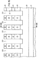
Figur 22 mit XIV-XIV bezeichneten Schnitt. Figur 25- zeigt eine Schaltung zum Einschreiben von Information in eine Speicherzellenanordnung mit ersten Wortleitungen und zweiten Wortleitungen.
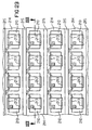
Figur 26- zeigt eine Schaltung zum Auslesen einer Speicherzellenanordnung mit ersten Wortleitungen und zweiten Wortleitungen und streifenförmigen, vergrabenen Bitleitungen.
- Figure 1
- shows a section through a semiconductor substrate with a first trench mask.
- Figure 2
- shows the section through the semiconductor substrate after a first trench etching.
- Figure 3
- shows the section through the semiconductor substrate after formation of a second trench mask.
- Figure 4
- shows the section labeled IV-IV in FIG. The section drawn in FIG. 3 is designated III-III in FIG.
- Figure 5
- shows the section shown in Figure 4 after a second trench etching.
- Figure 6
- shows the section shown in Figure 3 after formation of a first dielectric layer and a first conductive layer.
- Figure 7
- shows the section designated VII-VII in FIG. The section shown in Figure 6 is designated VI-VI in Figure 7.
- Figure 8
- shows the section shown in Figure 6 through the semiconductor substrate after formation of first word lines, a second dielectric layer and second word lines.
- Figure 9
- shows the section designated IX-IX in FIG. In Figure 9, the section shown in Figure 8 is designated VIII-VIII.
- Figure 10
- 8 shows the section shown in FIG. 8 after formation of first n + -doped regions and second n + -doped regions and after deposition of an intermediate oxide layer, opening of contacts, after formation of a capacitor dielectric and a capacitor plate.
- Figure 11
- shows the section designated XI-XI in FIG. In Figure 11, the section shown in Figure 10 is designated XX.
- Figure 12
- shows the section designated XII-XII in Figure 10 and Figure 11. The sections shown in Figure 10 and Figure 11 are designated XX and XI-XI.
- Figure 13
- shows a section through a semiconductor substrate after formation of first trenches.
- Figure 14
- shows the section shown in FIG. 13 through the semiconductor substrate after formation of nitride spacers on the flanks of the first trenches and filling of the first trenches with an SiO 2 structure.
- Figure 15
- shows the section designated XV-XV in FIG. 14 through the semiconductor substrate after formation of second trenches. The section shown in Figure 14 is designated XIV-XIV.
- Figure 16
- shows the section shown in FIG. 14 through the semiconductor substrate after formation of a first gate dielectric and first word lines, which are covered with a second insulation structure.
- Figure 17
- shows the section designated XVII-XVII in FIG. 16 through the semiconductor substrate. The section through the semiconductor substrate shown in FIG. 16 is designated XVI-XVI in FIG.
- Figure 18
- shows the section shown in Figure 16 after a selective epitaxy to form a second auxiliary structure.
- Figure 19
- shows the section designated XIX-XIX in FIG. In Figure 19, the section shown in Figure 18 is designated XVIII-XVIII.
- Figure 20
- shows the section shown in FIG. 18 after etching back the first auxiliary structures, forming a second gate dielectric, second word lines and a third insulation structure and after an implantation.
- Figure 21
- shows the section designated by XXI-XXI in FIG. In Figure 21, the section shown in Figure 20 is entered with XX-XX.
- Figure 22
- shows the section shown in Figure 20 after formation of a capacitor dielectric and a capacitor plate.
- Figure 23
- shows the section designated by XXIII-XXIII in FIG.
- Figure 24
- shows the section designated XIV-XIV in FIG.
- Figure 25
- shows a circuit for writing information into a memory cell arrangement with first word lines and second word lines.
- Figure 26
- shows a circuit for reading out a memory cell arrangement with first word lines and second word lines and strip-shaped, buried bit lines.
Die Darstellungen in den Figuren sind nicht maßstabsgerecht.The representations in the figures are not to scale.
Ein Halbleitersubstrat, das mindestens im Bereich einer
Hauptfläche 11 monokristallines Silizium aufweist, umfaßt einen
p-dotierten Substratkörper 12, eine darauf angeordnete
n+-dotierte Siliziumschicht 13, eine darauf angeordnete erste
p-dotierte Schicht 14 und eine darauf angeordnete zweite p-dotierte
Siliziumschicht 15 (siehe Figur 1). Der p-dotierte
Substratkörper 12 weist eine Dotierstoffkonzentration von
1016 cm-3 auf. Die n+-dotierte Siliziumschicht 13 ist durch
epitaktisches Aufwachsen in einer Dicke von 500 nm erzeugt.
Sie weist eine Dotierstoffkonzentration von 1020 cm-3 auf.
Die erste p-dotierte Siliziumschicht 14 und die zweite p-dotierte
Siliziumschicht 15 sind epitaktisch aufgewachsen und
weisen gemeinsam eine Dicke von 500 nm auf. Die erste p-dotierte
Siliziumschicht 14 weist eine Dicke von 200 nm und
eine Dotierstoffkonzentration von 1017 cm-3 auf. Die zweite
p-dotierte Siliziumschicht 15 weist eine Dicke von 300 nm und
eine Dotierstoffkonzentration von 1016 cm-3 auf.A semiconductor substrate which has monocrystalline silicon at least in the region of a
Anschließend wird auf der Hauptfläche 11 eine erste Grabenmaske
16 durch Abscheidung und Strukturierung einer SiO2-Schicht
gebildet. Die SiO2-Schicht wird in einem TEOS-Verfahren
in einer Schichtdicke von 150 nm abgeschieden und
mit Hilfe einer Photolackmaske durch Trockenätzen mit CHF3,
O2 strukturiert. Die erste Grabenmaske 16 weist streifenförmige
Öffnungen auf, die eine Breite von 250 nm und einen gegenseitigen
Abstand von 250 nm haben. Die Breite und der Abstand
entsprechen jeweils einer in der verwendeten Technologie
minimal herstellbaren Strukturgröße F.A
Nach Entfernen der Photolackmaske, die zur Bildung der ersten
Grabenmaske 16 verwendet wurde, werden erste Gräben 17 geätzt,
wobei die erste Grabenmaske 16 als Ätzmaske in einem
Trockenätzprozeß mit HBr, He, O2, NF3 verwendet wird. Anschließend
wird die erste Grabenmaske 16 naßchemisch zum Beispiel
mit HF entfernt (siehe Figur 2). Die Tiefe der ersten
Gräben 17 beträgt 1100 nm. Damit reichen die ersten Gräben 17
bis in den p-dotierten Substratkörper 12 hinein. Aus der n+-dotierten
Siliziumschicht 13 werden dabei streifenförmige
Bitleitungen 13' gebildet.After removing the photoresist mask that was used to form the
Nachfolgend wird eine SiO2-Schicht 18 abgeschieden, die die
ersten Gräben 17 vollständig auffüllt. Die SiO2-Schicht 18
wird in einem TEOS-Verfahren in einer Schichtdicke von 200 nm
abgeschieden (siehe Figur 3). Auf der Oberfläche der SiO2-Schicht
18 wird eine Photolackmaske 19 gebildet, die streifenförmige
Öffnungen aufweist. Die streifenförmigen Öffnungen
der Photolackmaske 19 verlaufen quer zu den ersten Gräben 17
(siehe Figur 3 und Figur 4). Die streifenförmigen Öffnungen
in der Photolackmaske 19 weisen eine Breite von 250 nm und
einen gegenseitigen Abstand von 1250 nm auf.An SiO 2 layer 18 is subsequently deposited, which completely fills the
Durch Trockenätzen mit Ar, CF4, CHF3, N2, He wird aus der
SiO2-Schicht 18 eine zweite Grabenmaske 18' gebildet. Nachfolgend
wird die Photolackmaske 19 entfernt. Beim Strukturieren
der zweiten Grabenmaske 18' bleiben die ersten Gräben 17
mit SiO2 gefüllt. Durch Abscheiden einer SiO2-Schicht in einem
TEOS-Verfahren in einer Schichtdicke von 80 nm und anisotropes
Ätzen mit CHF3, O2 werden an zur Hauptfläche 11
senkrechten Flanken der zweiten Grabenmaske 18' SiO2-Spacer
19 gebildet (siehe Figur 5). A second trench mask 18 'is formed from the SiO 2 layer 18 by dry etching with Ar, CF 4 , CHF 3 , N 2 , He. The
Unter Verwendung der zweiten Grabenmaske 18' und der SiO2-Spacer
190 werden durch anisotropes Trockenätzen zweite Gräben
110 gebildet (siehe Figur 5). Die zweiten Gräben 110 werden
in einer Tiefe von 500 nm geätzt. Sie reichen bis in die
Bitleitungen 13' hinein, ohne die Bitleitungen 13' jedoch zu
durchtrennen. Die zweiten Gräben 110 müssen so tief sein, daß
die erste p-dotierte Siliziumschicht 14 sicher durchtrennt
ist. Die Weite der zweiten Gräben 110 beträgt 90 nm. Sie ist
im Vergleich zur Weite der streifenförmigen Öffnungen in der
zweiten Grabenmaske 18' um die Breite der SiO2-Spacer 190 reduziert.Using the second trench mask 18 'and the SiO 2 spacer 190,
Durch anisotropes Ätzen mit CHF3, O2 werden anschließend die
SiO2-Spacer 190 und der obere Bereich der zweiten Grabenmaske
18' selektiv zu Silizium geätzt. Dabei wird der in den ersten
Gräben 17 befindliche Teil der zweiten Grabenmaske 18' soweit
geätzt, daß in den Gräben 17 erste Isolationsstrukturen 18''
aus der zweiten Grabenmaske 18' gebildet werden (siehe Figur
6 und Figur 7). Die ersten Isolationsstrukturen 18'' bedecken
den Boden der ersten Gräben und reichen bis in den oberen Bereich
der Bitleitungen 13'. Die Flanken der ersten p-dotierten
Siliziumschicht 14, der zweiten p-dotierten Siliziumschicht
15 und im oberen Bereich der Bitleitungen 13' werden
dabei freigelegt. Die Höhe der ersten Isolationsstrukturen
18'' beträgt etwa 500 nm.The SiO 2 spacers 190 and the upper region of the second trench mask 18 'are then selectively etched to silicon by anisotropic etching with CHF 3 , O 2 . The part of the
Durch thermische Oxidation wird eine erste dielektrische
Schicht 111 aus SiO2 in einer Schichtdicke von 5 nm gebildet.
Auf die erste dielektrische Schicht 111 wird eine leitfähige
Schicht 112 aufgebracht. Die leitfähige Schicht 112 wird aus
in situ dotiertem Polysilizium in einer Schichtdicke von 80
nm gebildet. Als Dotierstoff wird Phosphor verwendet. Die Dotierstoffkonzentration
beträgt 1021 cm-3. Die leitfähige
Schicht 112 füllt die zweiten Gräben 110 vollständig auf. Die
ersten Gräben 17 werden von der leitfähigen Schicht 112 nicht
aufgefüllt (siehe Figur 6 und Figur 7). A
Durch anisotropes Ätzen mit He, HBr, Cl2, C2F6 wird die leitfähige
Schicht 112 selektiv zur ersten dielektrischen Schicht
111 geätzt. Dabei wird die leitfähige Schicht 112 bis in eine
Tiefe von 200 nm unterhalb der Hauptfläche 11 entfernt. Dabei
werden aus der leitfähigen Schicht 112 erste Wortleitungen
112' gebildet. Die Höhe der ersten Wortleitungen 112' wird so
bemessen, daß sie den Bereich, in dem die erste dielektrische
Schicht 111 die Flanken der ersten p-dotierten Siliziumschicht
14 bedeckt, sicher überdeckt. Die Wortleitung 112'
wird aus ringförmigen Elementen gebildet, die jeweils eine
der Halbleitersäulen umgeben. In Richtung der ersten Gräben
17 benachbarte ringförmige Elemente grenzen dabei aneinander
(siehe Figur 8 und Figur 9). Durch Abscheiden und Rückätzen
einer SiO2-Schicht werden die ersten Gräben 17 und die zweiten
Gräben 110 mit einer zweiten Isolationsstruktur 113 aufgefüllt.
Die SiO2-Schicht wird in einem TEOS-Verfahren in einer
Schichtdicke von 200 nm abgeschieden. Das Rückätzen erfolgt
mit CHF3, O2. Bei der Bildung der zweiten Isolationsstruktur
113 wird die Hauptfläche 11 außerhalb der ersten
Gräben 17 und der zweiten Gräben 110 freigelegt.The
Durch thermische Oxidation wird eine zweite dielektrische
Schicht 114 aus SiO2 in einer Schichtdicke von 5 nm gebildet.
Auf der zweiten dielektrischen Schicht 114 werden streifenförmige
zweite Wortleitungen 115 und darauf streifenförmige
Siliziumnitridstrukturen 116 erzeugt (siehe Figur 8 und Figur
9). Die zweiten Wortleitungen 115 verlaufen parallel zu den
Zweiten Gräben 110. Zur Bildung der zweiten Wortleitungen
werden eine zweite leitfähige Schicht und eine Siliziumnitridschicht
abgeschieden und mit Hilfe einer Photolackmaske
streifenförmig strukturiert. Dazu wird folgender Ätzprozeß
verwendet: CF4, O2, N2/ He, HBr, Cl2, C2F6. Die zweiten Wortleitungen
115 werden in einer Breite von 250 nm, einem Abstand
von 250 nm, einer Länge von 200 µm und einer Dicke von
150 nm gebildet. Die zweiten Wortleitungen 115 werden zum
Beispiel aus in situ dotiertem Polysilizium gebildet. Als Dotierstoff
ist Phosphor geeignet. Die Dotierstoffkonzentration
beträgt 1021 cm-3. Die streifenförmigen Siliziumnitridstrukturen
116 weisen dieselben Abmessungen wie die zweiten Wortleitungen
115 auf und weisen eine Dicke von 50 nm auf.A
Durch Abscheiden einer Siliziumnitridschicht und anisotropes Ätzen der Siliziumnitridschicht werden an den Flanken der zweiten Wortleitungen 115 Siliziumnitridspacer gebildet. Die Siliziumnitridschicht wird in einem CVD-Verfahren in einer Schichtdicke von 30 nm abgeschieden. Die Ätzung erfolgt mit CF4, O2, N2. Die Ätzung erfolgt selektiv zu SiO2.By depositing a silicon nitride layer and anisotropically etching the silicon nitride layer, 115 silicon nitride spacers are formed on the flanks of the second word lines. The silicon nitride layer is deposited in a CVD process in a layer thickness of 30 nm. The etching is done with CF 4 , O 2 , N 2 . The etching is selective to SiO 2 .
Unter Verwendung einer Photolackmaske (nicht dargestellt) als
Implantationsmaske werden nachfolgend erste n+-dotierte Gebiete
118 gebildet. Die ersten n+-dotierten Gebiete 118 sind
jeweils zwischen benachbarten ersten Gräben 17 angeordnet,
grenzen an die Hauptfläche 11 und grenzen an die Grenzfläche
zur ersten p-dotierten Siliziumschicht 14 an. In jeder Halbleitersäule,
die durch jeweils benachbarte erste Gräben 17
und zweite Gräben 110 definiert wird, ist ein erstes n+-dotiertes
Gebiet 118 vorgesehen. Es befindet sich in etwa in
der Mitte zwischen benachbarten zweiten Gräben 110 (siehe Figur
10 und Figur 11). Die ersten n+-dotierten Gebiete 118
weisen eine Dotierstoffkonzentration von 1021 cm-3 auf und
eine Tiefe von 300 nm. Die Implantation erfolgt mit Phosphor
oder mit Arsen.Using a photoresist mask (not shown) as an implantation mask, first n + -doped
Nach Entfernen der Photolackmaske wird eine weitere Photolackmaske
(nicht dargestellt) gebildet, die als Implantationsmaske
zur Bildung zweiter n+-dotierter Gebiete 119 verwendet
wird. In jeder Halbleitersäule werden zwei n+-dotierte
Gebiete 119 gebildet, die beiderseits des jeweiligen ersten
n+-dotierten Gebietes 118 zwischen benachbarten zweiten Gräben
110 angeordnet sind. Zwischen dem zweiten n+-dotierten
Gebiet 119 und dem ersten n+-dotierten Gebiet 118 grenzt jeweils
die zweite p-dotierte Siliziumschicht 15 an die
Hauptfläche 11 an. Die Tiefe der zweiten n+-dotierten Gebiete
119 beträgt 100 nm. Sie ist geringer als die Dicke der zweiten
dotierten Siliziumschicht 15. Die Implantation erfolgt
mit Phosphor. Zwischen dem ersten n+-dotierten Gebiet 118 und
jedem der zweiten n+-dotierten Gebiete 119 verläuft an der
Oberfläche der Halbleitersäulen eine der zweiten Wortleitungen
115 (siehe Figur 11). Anschließend wird eine SiO2-Schicht
120 abgeschieden und durch chemisch-mechanisches Polieren
(CMP) planarisiert. Die planare Oberfläche der SiO2-Schicht
120 ist etwa 500 nm oberhalb der Hauptfläche 11 angeordnet.After the photoresist mask has been removed, a further photoresist mask (not shown) is formed, which is used as an implantation mask to form second n + -doped
Mit einer Photolackmaske und anisotropem Ätzen zum Beispiel
mit Ar, CF4, CHF3 werden nachfolgend Kontaktlöcher zu den
zweiten n+-dotierten Gebieten 119 in der SiO2-Schicht 120 geöffnet.
Die Kontaktlöcher werden mit Speicherknoten 121 versehen.
Dazu wird ganzflächig eine dotierte Polysiliziumschicht
abgeschieden und durch chemisch-mechanisches Polieren
planarisiert. Die Speicherknoten 121 werden mit Phosphor mit
einer Dotierstoffkonzentration von 1021 cm-3 in situ dotiert.Contact holes to the second n + -doped
Zum Öffnen der Kontaktlöcher für die Speicherknoten 121 ist
zwar eine photolithographisch erzeugte Photolackmaske erforderlich.
Deren Justierung ist jedoch unkritisch, da die zweiten
Wortleitungen 115 vollständig mit Siliziumnitrid bedeckt
sind und die Kontaktlochätzung selektiv zu Siliziumnitrid erfolgt
und somit eine Dejustage der Photolackmaske unkritisch
ist.To open the contact holes for the
Nachfolgend wird ein Kondensatordielektrikum 122 aus SiO2,
einer Dreifachschicht aus SiO2, Si3N4 und SiO2 oder einer
ferroelektrischen Schicht aus BST (Barium-Strontium-Titanat)
oder SBT (Strontium-Wismuth-Tantalat)abgeschieden. Das Kondensatordielektrikum
122 wird in einer Schichtdicke von 4 nm
abgeschieden. Auf das Kondensatordielektrikum 122 wird eine
Kondensatorplatte 123 aus dotiertem Polysilizium aufgebracht.
Die Kondensatorplatte 123 wird durch in situ dotierte Abscheidung
von Polysilizium mit Phosphor als Dotierstoff und
einer Dotierstoffkonzentration von 1021 cm-3 gebildet. A
In diesem Ausführungsbeispiel umfaßt jede Halbleitersäule,
die durch jeweils zwei benachbarte erste Gräben 17 und zweite
Gräben 110 definiert ist, zwei Speicherzellen. Diese zwei
Speicherzellen weisen einen gemeinsamen ersten Auswahltransistor
auf, der aus der Bitleitung 13', dem ersten n+-dotierten
Gebiet 118 als Source-/Drain-Gebiete und dem dazwischen angeordnete
Teil der ersten p-dotierten Siliziumschicht 14 als
Kanalgebiet, dem ersten Gatedielektrikum 11' und der ersten
Wortleitung 112' gebildet wird. Jede der speicherzellen weist
darüber hinaus einen zweiten Auswahltransistor auf, der jeweils
aus dem ersten n+-dotierten Gebiet 118 und einem der
zweiten n+-dotierten Gebiete 119 als Source-/Drain-Gebiete
sowie dem dazwischen angeordneten Teil der zweiten p-dotierten
Siliziumschicht 15 als Kanalgebiet, der zweiten
dielektrischen Schicht 114 als Gatedielektrikum und der oberhalb
des Kanalgebiets angeordneten zweiten Wortleitung 115
gebildet wird. Über das erste n+-dotierte Gebiet 118 sind die
beiden zweiten Auswahltransistoren mit dem gemeinsamen ersten
Auswahltransistor in Reihe verschaltet. Die oberhalb der
zweiten Gräben 110 angeordneten zweiten Wortleitungen 115 haben
in dieser Speicherzellenanordnung keine elektrische Funktion.
Ihre Funktion besteht darin, die Kontaktlochätzung für
die Speicherknoten 121 selektiv zu Siliziumnitrid zu ermöglichen.In this exemplary embodiment, each semiconductor column, which is defined by two adjacent
Die Einsatzspannung des gemeinsamen ersten Auswahltransistors
wird über die Dotierung der ersten p-dotierten Siliziumschicht
14 eingestellt. Die Einsatzspannung der zweiten Auswahltransistoren
wird über die Dotierung der zweiten p-dotierten
Siliziumschicht 15 eingestellt. Alternativ kann die
Einsatzspannung der zweiten Auswahltransistoren durch eine
spezielle Kanalimplantation eingestellt werden.The threshold voltage of the common first selection transistor
is about the doping of the first p-doped
Die ersten Wortleitungen 112' verlaufen quer zu den zweiten
Wortleitungen 115 und weisen ringförmige Elemente auf, die
jeweils eine der Halbleitersäulen umgeben (siehe Figur 12). The
Werden die ersten Gräben 17 mit einer Breite von einer minimal
herstellbaren Strukturgröße F und einem Abstand von F gebildet
und die zweiten Gräben 110 mit einer Breite von F abzüglich
der Breite der SiO2-Spacer 190 und einem Abstand zwischen
benachbarten zweiten Gräben 110 von 5F zuzüglich der
Breite der Si02-Spacer 190 so ergibt sich für jeweils zwei
Speicherzellen ein Platzbedarf von 12F2. Das heißt, die Speicherzellenanordnung
ist mit einem Flächenbedarf pro Speicherzelle
von 6F2 herstellbar.The
In einem zweiten Ausführungsbeispiel wird ein Halbleitersubstrat
verwendet, das ein SOI-Substrat 21 umfaßt, auf das
eine erste n+-dotierte Siliziumschicht 22, eine erste p-dotierte
Siliziumschicht 23, eine zweite n+-dotierte Siliziumschicht
24, eine zweite p-dotierte Siliziumschicht 25 und
eine dritte n+-dotierte Schicht 26 epitaktisch aufgewachsen
werden. Die dritte n+-dotierte Schicht 26 grenzt an eine
Hauptfläche 27 an (siehe Figur 13). Die erste n+-dotierte Siliziumschicht
22 wird in einer Schichtdicke von 300 nm mit
dem Dotierstoff As und einer Dotierstoffkonzentration von 1 x
1020 cm-3 gebildet. Die erste p-dotierte Siliziumschicht 23
wird in einer Schichtdicke von 200 nm mit einer Dotierstoffkonzentration
von 1 x 1018 cm-3 Bor gebildet. Die zweite
n+-dotierte Schicht 24 wird in einer Schichtdicke von 100 nm
mit einer Dotierstoffkonzentration von 1 x 1019 cm-3 und dem
Dotierstoff As gebildet. Die zweite p-dotierte Siliziumschicht
25 wird in einer Schichtdicke von 200 nm mit einer
Dotierstoffkonzentration von 1 x 1018 cm-3 mit Bor gebildet.
Die dritte n+-dotierte Schicht 26 wird in einer Schichtdicke
von 200 nm mit einer Dotierstoffkonzentration von 1 x 10¹⁹
cm-3 mit dem Dotierstoff As gebildet.In a second exemplary embodiment, a semiconductor substrate is used which comprises an
Auf der Hauptfläche 27 wird durch Abscheidung und Strukturierung
einer SiO2-Schicht eine erste Grabenmaske 28 gebildet.
Die SiO2-Schicht wird in einem TEOS-Verfahren in einer
Schichtdicke von 150 nm abgeschieden. Unter Verwendung einer
Photolackmaske wird sie durch anisotropes Ätzen mit CHF3, O2
strukturiert. Nach Entfernen der Photolackmaske werden erste
Gräben 29 geätzt. Die ersten Gräben 29 werden durch anisotropes
Ätzen mit HBr, He, O2, NF3 erzeugt. Die ersten Gräben 29
reichen bis in die erste n+-dotierte Siliziumschicht 22 hinein.
Die ersten Gräben 29 sind streifenförmig und weisen eine
Breite von 200 nm und einen Abstand zwischen benachbarten ersten
Gräben 29 von 200 nm auf. Die Länge der ersten Gräben 29
beträgt 5 µm und die Tiefe 800 nm.A
Nach Entfernen der ersten Grabenmaske 28 durch naßchemisches
Ätzen mit HF werden an zur Hauptfläche 27 im wesentlichen
senkrechten Flanken der ersten Gräben 29 Siliziumnitridspacer
210 gebildet. Dazu wird eine Siliziumnitridschicht in einer
Dicke von 70 nm abgeschieden und anisotrop mit CF4, O2, N2
selektiv zu Silizium geätzt. Die Dicke der Nitridschicht entspricht
einem Drittel der Weite der ersten Gräben 29.After removal of the
Der zwischen den Siliziumspacern 210 verbliebene Zwischenraum
wird nachfolgend mit einer ersten Isolationsstruktur 211 aufgefüllt.
Dazu wird eine SiO2-Schicht in einem TEOS-Verfahren
abgeschieden und anisotrop mit CHF3, O2 rückgeätzt, bis die
Hauptfläche 27 freigelegt ist (siehe Figur 14).The space remaining between the
Auf der Hauptfläche 27 wird eine zweite Grabenmaske durch Abscheiden
einer SiO2-Schicht und einer Siliziumnitridschicht
gebildet. Die SiO2-Schicht wird in einem TEOS-Verfahren mit
einer Dicke von 150 nm abgeschieden. Die Dicke der Siliziumnitridschicht
beträgt 70 nm. Unter Verwendung einer Photolackmaske
wird durch anisotropes Ätzen mit CHF3, O2 die Nitridschicht
und die SiO2-Schicht strukturiert. Nach Entfernen
der Photolackmaske werden zweite Gräben 212 erzeugt. Dabei
wird zunächst Silizium anisotrop mit HBr, He, O2, NF3 geätzt.
Nachfolgend wird SiO2 selektiv zu Nitrid mit C2F6, C3F8 geätzt,
wobei die Siliziumnitridschicht der zweiten Grabenmaske
als Hartmaske dient. Anschließend werden die Siliziumnitridspacer
und gleichzeitig die Siliziumnitrid-Hartmaske naßchemisch
mit H3PO4 entfernt. A second trench mask is formed on the
Die zweiten Gräben 212 verlaufen im wesentlichen senkrecht zu
den ersten Gräben 29 (siehe Figur 15, in der der in Figur 14
mit XV-XV dargestellte Schnitt gezeigt wird). Die zweiten
Gräben 212 weisen einen streifenförmigen Querschnitt auf mit
einer Breite von 200 nm, einem Abstand zwischen benachbarten
zweiten Gräben 212 von 200 nm und einer Länge von 5 µm. Die
Tiefe der zweiten Gräben 212 beträgt 800 nm. Die zweiten Gräben
212 reichen damit ebenfalls bis in die erste n+-dotierte
Siliziumschicht 22 hinein.The
Anschließend wird die erste Isolationsstruktur 211 entfernt.
Dieses erfolgt durch naßchemisches Ätzen von Siliziumoxid selektiv
zu Siliziumnitrid und Silizium mit HF.The
Durch thermische Oxidation wird ein erstes Gateoxid 213 in
einer Dicke von 5 nm gebildet. Durch Abscheiden einer in situ
dotierten Polysiliziumschicht und anisotropes Ätzen der dotierten
Polysiliziumschicht werden nachfolgend erste Wortleitungen
214 gebildet. Die dotierte Polysiliziumschicht wird
mit Phosphor dotiert abgeschieden. Sie weist eine Dicke von
70 nm auf. Das entspricht einem Drittel der Weite der ersten
Gräben 29 sowie der zweiten Gräben 212. Damit wird der Zwischenraum
zwischen den an gegenüberliegenden Flanken eines
der ersten Gräben 29 angeordneten Siliziumnitridspacern 210
aufgefüllt, die zweiten Gräben 212, deren im wesentlichen
senkrecht zur Hauptfläche 27 verlaufende Flanken nur mit dem
dünnen ersten Gateoxid 213 bedeckt sind, jedoch nicht. Das
Ätzen der dotierten Polysiliziumschicht erfolgt anisotrop mit
He, HBr, Cl2, C2F6. Das anisotrope Ätzen wird solange fortgesetzt,
bis die Wortleitungen in der Höhe im Bereich der zweiten
n+-dotierten Siliziumschicht 24 liegen. Die ersten Wortleitungen
214 überdecken in der Höhe die erste p-dotierte Siliziumschicht
23 vollständig (siehe Figur 16 und Figur 17).A
Teile der ersten Wortleitungen 214 umgeben jeweils eine der
Halbleitersäulen, die durch jeweils zwei benachbarte erste
Gräben 29 und zweite Gräben 212 definiert werden, ringförmig.
Der zwischen den Siliziumnitridspacern 210 verbliebene Freiraum
in den ersten Gräben 29 ist dabei vollständig mit den
ersten Wortleitungen 214 aufgefüllt. In den ersten Gräben 29
grenzen daher ringförmige Elemente der ersten Wortleitungen
214 zusammen. Die ersten Wortleitungen 214 werden somit gebildet
durch aneinandergrenzende ringförmige Elemente.Parts of the
Anschließend wird durch Abscheidung einer SiO2-Schicht und
anisotropes Rückätzen eine zweite Isolationsstruktur 215 gebildet,
die in den zweiten Gräben 212 den zwischen benachbarten
ersten Wortleitungen 214 verbliebenen Freiraum auffüllt.
Die Höhe der zweiten Isolationsstruktur 215 ist größer als
die der ersten Wortleitungen 214. Die zweite Isolationsstruktur
215 reicht maximal bis an die Grenzfläche zwischen der
zweiten n+-dotierten Siliziumschicht 24 und der zweiten p-dotierten
Siliziumschicht 25. Die Abscheidung der SiO2-Schicht
erfolgt in einem TEOS-Verfahren. Es wird anisotrop
geätzt mit Ar, CF4, CHF3. Bei dieser anisotropen Ätzung wird
auf der Hauptfläche 27 und im oberen Bereich der zweiten Gräben
212 befindliches erstes Gateoxid ebenfalls entfernt.Subsequently, a
Durch selektive Epitaxie werden nachfolgend auf freiliegenden
Siliziumoberflächen Siliziumstrukturen 216 aufgewachsen. Die
selektive Epitaxie erfolgt im Temperaturbereich von 700°C bis
900°C unter Verwendung eines Silan enthaltenden Prozeßgases.
Die Siliziumstrukturen 216 bedecken die freiliegenden Flanken
im Bereich der zweiten Gräben 212 oberhalb der zweiten Isolationsstruktur
215. Ferner bedecken sie die Oberfläche der
dritten n+-dotierten Siliziumschicht 26. Die Siliziumstrukturen
216 weisen eine Abmessung von 70 nm senkrecht zu der Siliziumoberfläche,
auf der sie aufwachsen, auf. Das entspricht
einem Drittel der Weite der zweiten Gräben 212. Die zweiten
Gräben 212 werden daher nicht aufgefüllt. Die Flanken der ersten
Gräben 29 sind durch die Siliziumnitridspacer 210 bedeckt,
so daß an den Flanken der ersten Gräben 29 kein Silizium
aufwächst (siehe Figur 18 und Figur 19).
Durch naßchemisches Ätzen mit H3PO4 wird Siliziumnitrid selektiv
zu Silizium angegriffen. Durch eine solche Ätzung werden
die Flanken der dritten n+-dotierten Siliziumschicht 26
und der zweiten p-dotierten Siliziumschicht 25 mindestens
teilweise freigelegt. Dadurch werden die Siliziumnitridspacer
210 in den ersten Gräben 29 in der Höhe reduziert (siehe Figur
20).Silicon nitride is selectively attacked to silicon by wet chemical etching with H 3 PO 4 . Such an etching exposes the flanks of the third n + -doped
Durch thermische Oxidation wird ein zweites Gateoxid 217 an
freiliegenden Siliziumflächen gebildet. Insbesondere entsteht
das zweite Gateoxid 217 an der freiliegenden Oberfläche der
zweiten p-dotierten Siliziumschicht 25 in den ersten Gräben
29 (siehe Figur 20 und Figur 21). Das zweite Gateoxid 217
wird in einer Schichtdicke von 5 nm gebildet.A
Durch Abscheiden einer in situ dotierten Polysiliziumschicht
und anisotropes Rückätzen der dotierten Polysiliziumschicht
werden zweite Wortleitungen 218 gebildet. Die in situ dotierte
Polysiliziumschicht wird mit Phosphor dotiert und weist
eine Dotierstoffkonzentration von 1021 cm-3 auf. Die dotierte
Polysiliziumschicht wird in einer Dicke von 70 nm abgeschieden.
Das entspricht einem Drittel der Weite der ersten Gräben
29 sowie der zweiten Gräben 212. Das anisotrope Ätzen wird
solange fortgesetzt, bis die Flanken der dritten n+-dotierten
Siliziumschicht 26 im Bereich der ersten Gräben 29 teilweise
freigelegt sind (siehe Figur 20).Second word lines 218 are formed by depositing an in-situ doped polysilicon layer and anisotropically etching back the doped polysilicon layer. The in-situ doped polysilicon layer is doped with phosphorus and has a dopant concentration of 10 21 cm -3 . The doped polysilicon layer is deposited to a thickness of 70 nm. This corresponds to a third of the width of the
Da die Weite der zweiten Gräben 212 im Bereich der Hauptfläche
durch die Siliziumstrukturen 216 auf etwa ein Drittel reduziert
ist, füllt die dotierte Polysiliziumschicht die zweiten
Gräben 212 auf. Entsprechend füllen die zweiten Wortleitungen
218 die zweiten Gräben in der Weite auf. Die zweiten
Wortleitungen 218 umfassen ringförmige Elemente, die jeweils
eine der Siliziumsäulen umgeben. In den zweiten Gräben 212
stoßen benachbarte ringförmige Elemente aneinander, so daß
die zweiten Wortleitungen 218 als Kette aneinander angrenzender
ringförmiger Elemente gebildet werden.Since the width of the
Die ersten Gräben 29 werden mit einer dritten Isolationsstruktur
219 aufgefüllt. Dazu wird eine SiO2-Schicht in
einem TEOS-Verfahren abgeschieden und anisotrop mit CHF3, O2
geätzt. Die dritte Isolationsstruktur 219 schließt in der Höhe
mit der Hauptfläche 27 ab.The
Durch Implantation mit Arsen mit einer Energie von 20 keV und
einer Dosis von 1014 cm-2 werden an der Hauptfläche 27 angeordnete
Speicherknoten 220 gebildet. Die Speicherknoten 220
werden aus den an der Hauptfläche 27 befindlichen Teilen der
Siliziumstruktur 216 gebildet. Die Speicherknoten 219 sind
mit der dritten n+-dotierten Siliziumschicht 26 elektrisch
verbunden.By implantation with arsenic with an energy of 20 keV and a dose of 10 14 cm -2 ,
Anschließend wird ganzflächig ein Kondensatordielektrikum 221
abgeschieden. Das Kondensatordielektrikum 221 wird aus SiO2,
einer Dreifachschicht aus SiO2, Si3N4 und SiO2 oder einem
Hochepsilon-Dielektrikum, zum Beispiel BST (Barium-Strontium-Titanat)
oder SBT (Strontium-Wismuth-Tantalat) gebildet.A
Auf das Kondensatordielektrikum 221 wird eine Kondensatorplatte
222 aufgebracht. Die Kondensatorplatte 221 wird durch
in situ dotierte Abscheidung von Polysilizium in einer
Schichtdicke von 200 nm und Planarisierung der dotierten Polysiliziumschicht
gebildet. Die dotierte Polysiliziumschicht
ist mit Phosphor mit einer Dotierstoffkonzentration von 1021
cm-3 dotiert (siehe Figur 22).A
Figur 23 zeigt den in Figur 22 mit XXIII-XXIII bezeichneten
Schnitt. Figur 24 zeigt den in Figur 22 mit XXIV-XXIV bezeichneten
Schnitt. Die ersten Wortleitungen 214 und die
zweiten Wortleitungen 218 sind jeweils als Kette ringförmiger
Elemente ausgebildet und verlaufen untereinander jeweils parallel.
Die ersten Wortleitungen 214 und die zweiten Wortleitungen
218 verlaufen quer zueinander.FIG. 23 shows that designated XXIII-XXIII in FIG. 22
Cut. FIG. 24 shows that designated XXIV-XXIV in FIG. 22
Cut. The
In dieser Ausführungsform der Speicherzellenanordnung umfaßt
jede Halbleitersäule, die jeweils durch zwei benachbarte erste
Gräben 29 und zweite Gräben 212 definiert wird, eine
Speicherzelle. Die Speicherzelle weist einen ersten Auswahltransistor
auf, der aus der ersten n+-dotierten Siliziumschicht
22 und der zweiten n+-dotierten Siliziumschicht 24
als Source-/Drain-Gebiete, der ersten p-dotierten Siliziumschicht
23 als Kanalbereich, dem ersten Gateoxid 213 und der
ersten Wortleitung 214 als Gateelektrode gebildet wird. Ein
zweiter Auswahltransistor der Speicherzelle wird aus der
zweiten n+-dotierten Siliziumschicht 24 und der dritten n+-dotierten
Siliziumschicht 26 als Source-/Drain-Gebiet, der
zweiten p-dotierten Siliziumschicht 25 als Kanalbereich, dem
zweiten Gateoxid 217 und der zweiten Wortleitung 218 als Gateelektrode
gebildet. Der erste Auswahltransistor und der
zweite Auswahltransistor sind über die zweite n+-dotierte Siliziumschicht
24, die als gemeinsames Source-/Drain-Gebiet
wirkt, in Reihe verschaltet. Die erste n+-dotierte Siliziumschicht
22 wirkt als gemeinsame Bitleitung.In this embodiment of the memory cell arrangement, each semiconductor column, which is defined in each case by two adjacent
In einer Variante dieses Ausführungsbeispiels wird die zweite
n+-dotierte Siliziumschicht 24 durch eine p-dotierte Siliziumschicht
ersetzt. In diesem Fall umfaßt jede Speicherzelle
nur einen Auswahltransistor, der jedoch über zwei Gateelektroden
angesteuert wird, die übereinander angeordnet sind und
deren Streufelder so groß sind, daß sie sich überlappen. Die
überlappenden Streufelder führen im eingeschalteten Zustand
dazu, daß sich ein leitender Kanal von der ersten n+-dotierten
Siliziumschicht 22 zur dritten n+-dotierten Siliziumschicht
26 durch alle p-dotierten Siliziumschichten hindurch
ausbildet. Der Auswahltransistor wirkt wie zwei in Reihe
verschaltete Auswahltransistoren, da sich ein leitender
Kanal nur bei Ansteuerung beider Gateelektroden ausbildet. In a variant of this exemplary embodiment, the second n + -doped
Zum Einschreiben einer Information in einer Speicherzellenanordnung mit ersten Wortleitungen WLXi, i = 1 bis n, und zweiten Wortleitungen WLYi, i = 1 bis n, und einer gemeinsamen Bitleitungsplatte BLP wird ein Datenwort über eine Datenleitung DL in ein erstes Schieberegister SR1 eingelesen. Parallel dazu wird das Datenwort über einen Inverter I invertiert und in ein zweites Schieberegister SR2 eingelesen. Die Ausgänge des ersten Schieberegisters SR1 sind über einen Schalter S1 mit den ersten Wortleitungen WLXi, i = 1 bis n, verbunden. Die Ausgänge des zweiten Schieberegisters sind über einen Schalter S0 mit den ersten Wortleitungen WLXi, i =1 bis n, verbunden.For writing information into a memory cell arrangement with first word lines WLXi, i = 1 to n, and second Word lines WLYi, i = 1 to n, and a common one Bit line plate BLP becomes a data word over a data line DL read into a first shift register SR1. Parallel for this purpose the data word is inverted via an inverter I. and read into a second shift register SR2. The exits of the first shift register SR1 are via a switch S1 connected to the first word lines WLXi, i = 1 to n. The outputs of the second shift register are over a switch S0 with the first word lines WLXi, i = 1 to n, connected.
Zum Einschreiben einer Information mit dem logischen Wert Eins wird der Schalter S1 so angesteuert, daß die Ausgänge des ersten Schieberegisters SR1 mit den ersten Wortleitungen WLXi, i = 1 bis n, verbunden sind. Die Bitleitungsplatte BLP wird mit einem Spannungswert beaufschlagt, der einer logischen Eins entspricht. Über die ersten Wortleitungen WLXi, i = 1 bis n, und die zweite Wortleitung WLYi, i = 1, werden die einzelnen Speicherzellen angesteuert, in denen eine logische Eins gespeichert wird. Auf diese Weise werden ohne Umladung der Bitleitungsplatte BLP alle Speicherzellen entlang der zweiten Wortleitung WLYi, i = 1, mit einer Eins beschrieben, in denen eine Eins gespeichert werden soll.For writing information with the logical value One of the switches S1 is controlled so that the outputs of the first shift register SR1 with the first word lines WLXi, i = 1 to n, are connected. The bit line plate BLP is supplied with a voltage value that is a logical One corresponds. Via the first word lines WLXi, i = 1 to n, and the second word line WLYi, i = 1, become the controlled individual memory cells in which a logical One is saved. This way, without transhipment the bit line plate BLP all memory cells along the second word line WLYi, i = 1, described with a one, in which a one should be stored.
Anschließend wird die Verbindung zwischen den ersten Wortleitungen WLXi, i = 1 bis n, und dem ersten Schieberegister SR1 durch entsprechende Ansteuerung des Schalters S1 getrennt und die Bitleitungsplatte BLP mit einem Spannungspegel beaufschlagt, der einer logischen Null entspricht. Nachfolgend wird der Schalter S0 so angesteuert, daß das zweite Schieberegister mit den ersten Wortleitungen WLXi, i = 1 bis n, verbunden ist. Nachfolgend werden über die ersten Wortleitungen WLXi, i = 1 bis n, und die zweiten Wortleitungen WLYi, i = 1, die einzelnen Speicherzellen angesteuert, in denen eine logische Null gespeichert werden soll. Das nächste Datenwort wird entsprechend eingelesen, wobei jetzt die zweite Wortleitung WLYi, i = 2, eingeschaltet wird. Für das Einlesen der folgenden Datenwörter wird der Laufindex i der zweiten Wortleitung WLYi weiter inkrementiert (siehe Figur 25).Then the connection between the first word lines WLXi, i = 1 to n, and the first shift register SR1 separated by appropriate control of switch S1 and a voltage level is applied to the bit line plate BLP, which corresponds to a logical zero. Below the switch S0 is driven so that the second shift register connected to the first word lines WLXi, i = 1 to n is. Below are about the first word lines WLXi, i = 1 to n, and the second word lines WLYi, i = 1, controlled the individual memory cells in which a logical Zero should be saved. The next data word is read accordingly, now using the second word line WLYi, i = 2, is switched on. For reading the following Data words become the run index i of the second word line WLYi incremented further (see Figure 25).
Zum Auslesen einer Speicherzellenanordnung mit ersten Wortleitungen WLXi, i = 1 bis n, und zweiten Wortleitungen WLYi, i = 1 bis n, und streifenförmigen Bitleitungen BLi, i = 1 bis n, werden die einzelnen Speicherzellen, die entlang einer streifenförmigen Bitleitung BLi angeordnet sind, nacheinander über die zugehörige erste Wortleitung WLXi und die zugehörigen zweiten Wortleitungen WLYi, i = 1 bis n, angesteuert (siehe Figur 26). Das Auslesen der Daten erfolgt parallel für alle Bitleitungen BLi, i = 1 bis n. Dieses parallele Auslesen erfolgt innerhalb eines Zellenblockes ZB. Zusätzlich dazu können mehrere Zellenblöcke definiert werden, die darüber hinaus parallel ausgelesen werden. Dadurch wird die Zeit für den Datenzugriff verkürzt.For reading out a memory cell arrangement with first word lines WLXi, i = 1 to n, and second word lines WLYi, i = 1 to n, and strip-shaped bit lines BLi, i = 1 to n, the individual memory cells that are along a strip-shaped bit line BLi are arranged one after the other via the associated first word line WLXi and the associated second word lines WLYi, i = 1 to n, driven (see Figure 26). The data is read out in parallel for all bit lines BLi, i = 1 to n. This parallel readout takes place within a cell block ZB. Additionally You can define several cell blocks that are above be read out in parallel. This is the time for shortens data access.
Zum Refresh von Daten in einer DRAM-Zellenanordnung werden zunächst die gespeicherten Informationen, wie anhand von Figur 26 geschildert, ausgelesen in ein Schieberegister und anschließend, wie anhand von Figur 25 geschildert, wieder eingelesen. Der Vorteil dieses Betriebsverfahrens liegt darin, daß die gespeicherte Information, die ausgelesen wird, nur zur Ansteuerung einer Wortleitung und nicht zum Anheben des zugehörigen Pegels in der Speicherzelle verwendet wird.For refreshing data in a DRAM cell arrangement first of all the stored information, as with reference to figure 26 described, read out in a shift register and then, as described with reference to Figure 25, read again. The advantage of this operating method is that that the stored information that is read out only to control a word line and not to raise the associated level in the memory cell is used.
Claims (21)
bei der die Speicherzellen jeweils einen ersten Auswahltransistor und einen zweiten Auswahltransistor aufweisen, die in Reihe geschaltet sind und wobei der erste Auswahltransistor von der ersten Wortleitung und der zweite Auswahltransistor von der zweiten Wortleitung ansteuerbar ist.Memory cell arrangement according to claim 1 or 2,
in which the memory cells each have a first selection transistor and a second selection transistor, which are connected in series, and wherein the first selection transistor can be driven by the first word line and the second selection transistor by the second word line.
bei der der zweite Auswahltransistor als in Bezug auf die Hauptfläche (27) des Halbleitersubstrats vertikaler Transistor ausgestaltet ist.Memory cell arrangement according to claim 4,
in which the second selection transistor is designed as a vertical transistor with respect to the main surface (27) of the semiconductor substrate.
bei der die Speicherzellen jeweils nur einen Auswahltransistor aufweisen, der über die erste Wortleitung und die zweite Wortleitung ansteuerbar ist.Memory cell arrangement according to claim 1 or 2,
in which the memory cells each have only one selection transistor which can be driven via the first word line and the second word line.
bei der als Speicherelement eine Speicherkapazität vorgesehen ist. Memory cell arrangement according to one of claims 1 to 9,
in which a storage capacity is provided as the storage element.
bei dem Speicherzellen gebildet werden, die jeweils mindestens einen vertikalen Auswahltransistor aufweisen, der mit einem Speicherelement verbunden ist, und die jeweils über eine erste Wortleitung und eine zweite Wortleitung ansteuerbar sind, wobei sich die erste Wortleitung und die zweite Wortleitung kreuzen.Method for producing a memory cell arrangement,
in which memory cells are formed, each having at least one vertical selection transistor, which is connected to a memory element, and which can be controlled via a first word line and a second word line, the first word line and the second word line crossing.
bei dem die ersten Hilfsstrukturen und/oder die zweiten Hilfsstrukturen durch konformes Abscheiden und anisotropes Ätzen und/oder durch selektive Epitaxie gebildet werden.A method according to claim 15,
in which the first auxiliary structures and / or the second auxiliary structures are formed by conformal deposition and anisotropic etching and / or by selective epitaxy.
Applications Claiming Priority (2)
| Application Number | Priority Date | Filing Date | Title |
|---|---|---|---|
| DE19756183 | 1997-12-17 | ||
| DE19756183 | 1997-12-17 |
Publications (3)
| Publication Number | Publication Date |
|---|---|
| EP0924766A2 true EP0924766A2 (en) | 1999-06-23 |
| EP0924766A3 EP0924766A3 (en) | 2000-09-20 |
| EP0924766B1 EP0924766B1 (en) | 2008-02-20 |
Family
ID=7852307
Family Applications (1)
| Application Number | Title | Priority Date | Filing Date |
|---|---|---|---|
| EP98120336A Expired - Lifetime EP0924766B1 (en) | 1997-12-17 | 1998-10-27 | Memory cell array and method of its manufacture |
Country Status (7)
| Country | Link |
|---|---|
| US (1) | US6229169B1 (en) |
| EP (1) | EP0924766B1 (en) |
| JP (1) | JPH11243183A (en) |
| KR (1) | KR100560648B1 (en) |
| CN (1) | CN1169223C (en) |
| DE (1) | DE59814170D1 (en) |
| TW (1) | TW402816B (en) |
Cited By (24)
| Publication number | Priority date | Publication date | Assignee | Title |
|---|---|---|---|---|
| EP1179850A2 (en) * | 2000-08-11 | 2002-02-13 | Fujio Masuoka | A semiconductor memory and its production process |
| EP1246247A2 (en) * | 2001-03-30 | 2002-10-02 | Fujio Masuoka | A semiconductor memory and its production process |
| US6806140B1 (en) | 2000-06-15 | 2004-10-19 | Samsung Electronics Co., Ltd. | Semiconductor memory device for eliminating floating body effect and method of fabricating the same |
| DE10152911B4 (en) * | 2000-10-28 | 2005-11-24 | Samsung Electronics Co., Ltd., Suwon | Integrated circuit devices having extended effective width active regions, and methods of making same |
| US7732816B2 (en) | 2001-06-18 | 2010-06-08 | Innovative Silicon Isi Sa | Semiconductor device |
| US8861247B2 (en) | 2009-04-27 | 2014-10-14 | Micron Technology, Inc. | Techniques for providing a direct injection semiconductor memory device |
| US8947965B2 (en) | 2009-07-27 | 2015-02-03 | Micron Technology Inc. | Techniques for providing a direct injection semiconductor memory device |
| US8964479B2 (en) | 2010-03-04 | 2015-02-24 | Micron Technology, Inc. | Techniques for sensing a semiconductor memory device |
| US8982633B2 (en) | 2009-05-22 | 2015-03-17 | Micron Technology, Inc. | Techniques for providing a direct injection semiconductor memory device |
| US9019759B2 (en) | 2010-03-15 | 2015-04-28 | Micron Technology, Inc. | Techniques for providing a semiconductor memory device |
| US9019788B2 (en) | 2008-01-24 | 2015-04-28 | Micron Technology, Inc. | Techniques for accessing memory cells |
| US9064730B2 (en) | 2009-03-04 | 2015-06-23 | Micron Technology, Inc. | Techniques for forming a contact to a buried diffusion layer in a semiconductor memory device |
| US9093311B2 (en) | 2009-03-31 | 2015-07-28 | Micron Technology, Inc. | Techniques for providing a semiconductor memory device |
| US9142264B2 (en) | 2010-05-06 | 2015-09-22 | Micron Technology, Inc. | Techniques for refreshing a semiconductor memory device |
| US9240496B2 (en) | 2009-04-30 | 2016-01-19 | Micron Technology, Inc. | Semiconductor device with floating gate and electrically floating body |
| US9257155B2 (en) | 2007-05-30 | 2016-02-09 | Micron Technology, Inc. | Integrated circuit having voltage generation circuitry for memory cell array, and method of operating and/or controlling same |
| US9263133B2 (en) | 2011-05-17 | 2016-02-16 | Micron Technology, Inc. | Techniques for providing a semiconductor memory device |
| US9276000B2 (en) | 2007-03-29 | 2016-03-01 | Micron Technology, Inc. | Manufacturing process for zero-capacitor random access memory circuits |
| US9331083B2 (en) | 2009-07-10 | 2016-05-03 | Micron Technology, Inc. | Techniques for providing a semiconductor memory device |
| US9553186B2 (en) | 2008-09-25 | 2017-01-24 | Micron Technology, Inc. | Recessed gate silicon-on-insulator floating body device with self-aligned lateral isolation |
| US9559216B2 (en) | 2011-06-06 | 2017-01-31 | Micron Technology, Inc. | Semiconductor memory device and method for biasing same |
| US9812179B2 (en) | 2009-11-24 | 2017-11-07 | Ovonyx Memory Technology, Llc | Techniques for reducing disturbance in a semiconductor memory device |
| US10304837B2 (en) | 2007-11-29 | 2019-05-28 | Ovonyx Memory Technology, Llc | Integrated circuit having memory cell array including barriers, and method of manufacturing same |
| US10418091B2 (en) | 2005-09-07 | 2019-09-17 | Ovonyx Memory Technology, Llc | Memory cell and memory cell array having an electrically floating body transistor, and methods of operating same |
Families Citing this family (62)
| Publication number | Priority date | Publication date | Assignee | Title |
|---|---|---|---|---|
| DE19845004C2 (en) * | 1998-09-30 | 2002-06-13 | Infineon Technologies Ag | DRAM cell arrangement and method for its production |
| DE19911148C1 (en) * | 1999-03-12 | 2000-05-18 | Siemens Ag | DRAM cell array has single vertical transistor memory cells with buried bit lines and low space requirement |
| DE19929211B4 (en) * | 1999-06-25 | 2005-10-06 | Infineon Technologies Ag | A method of manufacturing a MOS transistor and a DRAM cell array |
| DE19943760C1 (en) * | 1999-09-13 | 2001-02-01 | Infineon Technologies Ag | DRAM cell arrangement comprises a substrate with a recess containing a storage node of a capacitor |
| DE10125967C1 (en) * | 2001-05-29 | 2002-07-11 | Infineon Technologies Ag | DRAM cell arrangement used for a semiconductor storage device comprises a matrix arrangement of storage cells stacked over each other as layers, and a capacitor connected to the MOS transistor |
| US6567329B2 (en) | 2001-08-28 | 2003-05-20 | Intel Corporation | Multiple word-line accessing and accessor |
| US6842369B2 (en) | 2002-05-07 | 2005-01-11 | Hewlett-Packard Development Company, L.P. | Intermesh memory device |
| US6734063B2 (en) * | 2002-07-22 | 2004-05-11 | Infineon Technologies Ag | Non-volatile memory cell and fabrication method |
| US20040228168A1 (en) | 2003-05-13 | 2004-11-18 | Richard Ferrant | Semiconductor memory device and method of operating same |
| US6777260B1 (en) * | 2003-08-14 | 2004-08-17 | Silicon Storage Technology, Inc. | Method of making sub-lithographic sized contact holes |
| US7042030B2 (en) * | 2003-11-21 | 2006-05-09 | Texas Instruments Incorporated | High density memory array |
| JP4593960B2 (en) * | 2004-04-14 | 2010-12-08 | 白土 猛英 | Semiconductor memory device |
| US7098105B2 (en) * | 2004-05-26 | 2006-08-29 | Micron Technology, Inc. | Methods for forming semiconductor structures |
| US7247570B2 (en) | 2004-08-19 | 2007-07-24 | Micron Technology, Inc. | Silicon pillars for vertical transistors |
| US7442976B2 (en) | 2004-09-01 | 2008-10-28 | Micron Technology, Inc. | DRAM cells with vertical transistors |
| KR100618875B1 (en) * | 2004-11-08 | 2006-09-04 | 삼성전자주식회사 | Semiconductor memory device having vertical channel MOS transistor and method for manufacturing the same |
| US7120046B1 (en) | 2005-05-13 | 2006-10-10 | Micron Technology, Inc. | Memory array with surrounding gate access transistors and capacitors with global and staggered local bit lines |
| US7371627B1 (en) | 2005-05-13 | 2008-05-13 | Micron Technology, Inc. | Memory array with ultra-thin etched pillar surround gate access transistors and buried data/bit lines |
| US7902598B2 (en) * | 2005-06-24 | 2011-03-08 | Micron Technology, Inc. | Two-sided surround access transistor for a 4.5F2 DRAM cell |
| US7888721B2 (en) | 2005-07-06 | 2011-02-15 | Micron Technology, Inc. | Surround gate access transistors with grown ultra-thin bodies |
| US7768051B2 (en) | 2005-07-25 | 2010-08-03 | Micron Technology, Inc. | DRAM including a vertical surround gate transistor |
| US7696567B2 (en) | 2005-08-31 | 2010-04-13 | Micron Technology, Inc | Semiconductor memory device |
| US7683430B2 (en) | 2005-12-19 | 2010-03-23 | Innovative Silicon Isi Sa | Electrically floating body memory cell and array, and method of operating or controlling same |
| US7476933B2 (en) * | 2006-03-02 | 2009-01-13 | Micron Technology, Inc. | Vertical gated access transistor |
| US7842558B2 (en) | 2006-03-02 | 2010-11-30 | Micron Technology, Inc. | Masking process for simultaneously patterning separate regions |
| US7492632B2 (en) | 2006-04-07 | 2009-02-17 | Innovative Silicon Isi Sa | Memory array having a programmable word length, and method of operating same |
| US7933142B2 (en) | 2006-05-02 | 2011-04-26 | Micron Technology, Inc. | Semiconductor memory cell and array using punch-through to program and read same |
| US8069377B2 (en) | 2006-06-26 | 2011-11-29 | Micron Technology, Inc. | Integrated circuit having memory array including ECC and column redundancy and method of operating the same |
| US7542340B2 (en) | 2006-07-11 | 2009-06-02 | Innovative Silicon Isi Sa | Integrated circuit including memory array having a segmented bit line architecture and method of controlling and/or operating same |
| US7666797B2 (en) * | 2006-08-17 | 2010-02-23 | Micron Technology, Inc. | Methods for forming semiconductor constructions, and methods for selectively etching silicon nitride relative to conductive material |
| US7692949B2 (en) * | 2006-12-04 | 2010-04-06 | Qimonda North America Corp. | Multi-bit resistive memory |
| KR101406604B1 (en) | 2007-01-26 | 2014-06-11 | 마이크론 테크놀로지, 인코포레이티드 | Floating-body dram transistor comprising source/drain regions separated from the gated body region |
| US8085594B2 (en) | 2007-06-01 | 2011-12-27 | Micron Technology, Inc. | Reading technique for memory cell with electrically floating body transistor |
| US7923373B2 (en) | 2007-06-04 | 2011-04-12 | Micron Technology, Inc. | Pitch multiplication using self-assembling materials |
| US8194487B2 (en) | 2007-09-17 | 2012-06-05 | Micron Technology, Inc. | Refreshing data of memory cells with electrically floating body transistors |
| US8349662B2 (en) | 2007-12-11 | 2013-01-08 | Micron Technology, Inc. | Integrated circuit having memory cell array, and method of manufacturing same |
| US8014195B2 (en) | 2008-02-06 | 2011-09-06 | Micron Technology, Inc. | Single transistor memory cell |
| US8189376B2 (en) | 2008-02-08 | 2012-05-29 | Micron Technology, Inc. | Integrated circuit having memory cells including gate material having high work function, and method of manufacturing same |
| KR101132302B1 (en) * | 2008-03-07 | 2012-04-05 | 주식회사 하이닉스반도체 | Method of manufacturing semiconductor device |
| KR101145396B1 (en) * | 2008-04-04 | 2012-05-16 | 에스케이하이닉스 주식회사 | Method for forming vertical gate and method for manufacturing semiconductor device using the same |
| US7957206B2 (en) | 2008-04-04 | 2011-06-07 | Micron Technology, Inc. | Read circuitry for an integrated circuit having memory cells and/or a memory cell array, and method of operating same |
| KR101037495B1 (en) * | 2008-07-31 | 2011-05-26 | 주식회사 하이닉스반도체 | Method of fabricating high integrated semiconductor apparatus and semiconductor apparatus fabricated thereby |
| US8101497B2 (en) | 2008-09-11 | 2012-01-24 | Micron Technology, Inc. | Self-aligned trench formation |
| US7933140B2 (en) | 2008-10-02 | 2011-04-26 | Micron Technology, Inc. | Techniques for reducing a voltage swing |
| US7924630B2 (en) | 2008-10-15 | 2011-04-12 | Micron Technology, Inc. | Techniques for simultaneously driving a plurality of source lines |
| US8223574B2 (en) | 2008-11-05 | 2012-07-17 | Micron Technology, Inc. | Techniques for block refreshing a semiconductor memory device |
| US8213226B2 (en) | 2008-12-05 | 2012-07-03 | Micron Technology, Inc. | Vertical transistor memory cell and array |
| US8319294B2 (en) | 2009-02-18 | 2012-11-27 | Micron Technology, Inc. | Techniques for providing a source line plane |
| US8199595B2 (en) | 2009-09-04 | 2012-06-12 | Micron Technology, Inc. | Techniques for sensing a semiconductor memory device |
| US8310893B2 (en) | 2009-12-16 | 2012-11-13 | Micron Technology, Inc. | Techniques for reducing impact of array disturbs in a semiconductor memory device |
| US8416636B2 (en) | 2010-02-12 | 2013-04-09 | Micron Technology, Inc. | Techniques for controlling a semiconductor memory device |
| US8411513B2 (en) | 2010-03-04 | 2013-04-02 | Micron Technology, Inc. | Techniques for providing a semiconductor memory device having hierarchical bit lines |
| US8369177B2 (en) | 2010-03-05 | 2013-02-05 | Micron Technology, Inc. | Techniques for reading from and/or writing to a semiconductor memory device |
| US8207041B2 (en) | 2010-03-09 | 2012-06-26 | Micron Technology, Inc. | Semiconductor processing methods |
| CN102222524B (en) * | 2010-04-14 | 2014-07-16 | 旺宏电子股份有限公司 | Method for operating memory cell |
| JP2013045894A (en) * | 2011-08-24 | 2013-03-04 | Rexchip Electronics Corp | Three-dimensional dram with auxiliary electrode structure |
| KR20130139599A (en) * | 2012-06-13 | 2013-12-23 | 에스케이하이닉스 주식회사 | Semiconductor device, electronic system and manufacturing method for the same |
| US9728266B1 (en) | 2016-07-08 | 2017-08-08 | Micron Technology, Inc. | Memory device including multiple select gates and different bias conditions |
| US11164879B2 (en) | 2018-11-16 | 2021-11-02 | International Business Machines Corporation | Microelectronic device with a memory element utilizing stacked vertical devices |
| US11171142B2 (en) | 2018-11-16 | 2021-11-09 | International Business Machines Corporation | Integrated circuit with vertical structures on nodes of a grid |
| US10833089B2 (en) | 2018-11-16 | 2020-11-10 | International Business Machines Corporation | Buried conductive layer supplying digital circuits |
| US10804266B2 (en) | 2018-11-16 | 2020-10-13 | International Business Machines Corporation | Microelectronic device utilizing stacked vertical devices |
Citations (4)
| Publication number | Priority date | Publication date | Assignee | Title |
|---|---|---|---|---|
| US4168538A (en) * | 1977-09-06 | 1979-09-18 | Siemens Aktiengesellschaft | Monolithically integrated semiconductor store |
| JPH02188958A (en) * | 1989-01-17 | 1990-07-25 | Mitsubishi Electric Corp | Dynamic memory structure |
| DE4312651A1 (en) * | 1992-04-24 | 1993-10-28 | Mitsubishi Electric Corp | Dynamic random-access memory - provides grouped memory cells each cell contg. capacitor and FET with transfer and sub-transfer gates having respective threshold voltages which alternate between high and low values between cells. |
| DE19519160C1 (en) * | 1995-05-24 | 1996-09-12 | Siemens Ag | DRAM cell arrangement having packing density required for specified memory |
Family Cites Families (11)
| Publication number | Priority date | Publication date | Assignee | Title |
|---|---|---|---|---|
| JPH0821689B2 (en) * | 1990-02-26 | 1996-03-04 | 株式会社東芝 | Semiconductor memory device and manufacturing method thereof |
| US5289432A (en) * | 1991-04-24 | 1994-02-22 | International Business Machines Corporation | Dual-port static random access memory cell |
| JPH05218349A (en) * | 1992-02-04 | 1993-08-27 | Sony Corp | Semiconductor storage device |
| US5208172A (en) * | 1992-03-02 | 1993-05-04 | Motorola, Inc. | Method for forming a raised vertical transistor |
| DE59608588D1 (en) * | 1995-09-26 | 2002-02-21 | Infineon Technologies Ag | Self-amplifying DRAM memory cell arrangement |
| KR970018065A (en) * | 1995-09-29 | 1997-04-30 | 김광호 | Method of manufacturing metal wiring |
| KR100198662B1 (en) | 1996-05-16 | 1999-06-15 | 구본준 | Dram cell, dram and its fabrication method |
| US5990509A (en) * | 1997-01-22 | 1999-11-23 | International Business Machines Corporation | 2F-square memory cell for gigabit memory applications |
| US6072209A (en) * | 1997-07-08 | 2000-06-06 | Micro Technology, Inc. | Four F2 folded bit line DRAM cell structure having buried bit and word lines |
| US5907170A (en) * | 1997-10-06 | 1999-05-25 | Micron Technology, Inc. | Circuit and method for an open bit line memory cell with a vertical transistor and trench plate trench capacitor |
| TW393731B (en) * | 1997-12-01 | 2000-06-11 | Nanya Plastics Corp | DRAM sharing a bit line contact window with multi-memory cells and its manufacturing method |
-
1998
- 1998-10-27 DE DE59814170T patent/DE59814170D1/en not_active Expired - Fee Related
- 1998-10-27 EP EP98120336A patent/EP0924766B1/en not_active Expired - Lifetime
- 1998-10-29 TW TW087117960A patent/TW402816B/en not_active IP Right Cessation
- 1998-12-16 CN CNB981253814A patent/CN1169223C/en not_active Expired - Fee Related
- 1998-12-16 JP JP10358127A patent/JPH11243183A/en not_active Abandoned
- 1998-12-17 US US09/213,724 patent/US6229169B1/en not_active Expired - Fee Related
- 1998-12-17 KR KR1019980055576A patent/KR100560648B1/en not_active IP Right Cessation
Patent Citations (4)
| Publication number | Priority date | Publication date | Assignee | Title |
|---|---|---|---|---|
| US4168538A (en) * | 1977-09-06 | 1979-09-18 | Siemens Aktiengesellschaft | Monolithically integrated semiconductor store |
| JPH02188958A (en) * | 1989-01-17 | 1990-07-25 | Mitsubishi Electric Corp | Dynamic memory structure |
| DE4312651A1 (en) * | 1992-04-24 | 1993-10-28 | Mitsubishi Electric Corp | Dynamic random-access memory - provides grouped memory cells each cell contg. capacitor and FET with transfer and sub-transfer gates having respective threshold voltages which alternate between high and low values between cells. |
| DE19519160C1 (en) * | 1995-05-24 | 1996-09-12 | Siemens Ag | DRAM cell arrangement having packing density required for specified memory |
Non-Patent Citations (1)
| Title |
|---|
| PATENT ABSTRACTS OF JAPAN vol. 014, no. 463 (E-0988), 8. Oktober 1990 (1990-10-08) & JP 02 188958 A (MITSUBISHI ELECTRIC CORP), 25. Juli 1990 (1990-07-25) * |
Cited By (37)
| Publication number | Priority date | Publication date | Assignee | Title |
|---|---|---|---|---|
| DE10128928B4 (en) * | 2000-06-15 | 2011-11-03 | Samsung Electronics Co., Ltd. | Semiconductor memory device that has no floating body effect, and associated manufacturing method |
| US6806140B1 (en) | 2000-06-15 | 2004-10-19 | Samsung Electronics Co., Ltd. | Semiconductor memory device for eliminating floating body effect and method of fabricating the same |
| US7135726B2 (en) | 2000-08-11 | 2006-11-14 | Fujio Masuoka | Semiconductor memory and its production process |
| EP1179850A2 (en) * | 2000-08-11 | 2002-02-13 | Fujio Masuoka | A semiconductor memory and its production process |
| EP1179850A3 (en) * | 2000-08-11 | 2006-02-22 | Fujio Masuoka | A semiconductor memory and its production process |
| US7521753B2 (en) | 2000-10-28 | 2009-04-21 | Samsung Electronics Co., Ltd. | Integrated circuit devices having active regions with expanded effective widths |
| US7187032B2 (en) | 2000-10-28 | 2007-03-06 | Samsung Electronics Co., Ltd | Integrated circuit devices having active regions with expanded effective widths |
| DE10152911B4 (en) * | 2000-10-28 | 2005-11-24 | Samsung Electronics Co., Ltd., Suwon | Integrated circuit devices having extended effective width active regions, and methods of making same |
| DE10152911B9 (en) * | 2000-10-28 | 2013-04-18 | Samsung Electronics Co., Ltd. | Integrated circuit devices having extended effective width active regions, and methods of making same |
| EP1246247A3 (en) * | 2001-03-30 | 2006-04-12 | Fujio Masuoka | A semiconductor memory and its production process |
| EP1246247A2 (en) * | 2001-03-30 | 2002-10-02 | Fujio Masuoka | A semiconductor memory and its production process |
| US7732816B2 (en) | 2001-06-18 | 2010-06-08 | Innovative Silicon Isi Sa | Semiconductor device |
| US11031069B2 (en) | 2005-09-07 | 2021-06-08 | Ovonyx Memory Technology, Llc | Memory cell and memory cell array having an electrically floating body transistor, and methods of operating same |
| US10418091B2 (en) | 2005-09-07 | 2019-09-17 | Ovonyx Memory Technology, Llc | Memory cell and memory cell array having an electrically floating body transistor, and methods of operating same |
| US9276000B2 (en) | 2007-03-29 | 2016-03-01 | Micron Technology, Inc. | Manufacturing process for zero-capacitor random access memory circuits |
| US9257155B2 (en) | 2007-05-30 | 2016-02-09 | Micron Technology, Inc. | Integrated circuit having voltage generation circuitry for memory cell array, and method of operating and/or controlling same |
| US11081486B2 (en) | 2007-11-29 | 2021-08-03 | Ovonyx Memory Technology, Llc | Integrated circuit having memory cell array including barriers, and method of manufacturing same |
| US10304837B2 (en) | 2007-11-29 | 2019-05-28 | Ovonyx Memory Technology, Llc | Integrated circuit having memory cell array including barriers, and method of manufacturing same |
| US9019788B2 (en) | 2008-01-24 | 2015-04-28 | Micron Technology, Inc. | Techniques for accessing memory cells |
| US9553186B2 (en) | 2008-09-25 | 2017-01-24 | Micron Technology, Inc. | Recessed gate silicon-on-insulator floating body device with self-aligned lateral isolation |
| US9064730B2 (en) | 2009-03-04 | 2015-06-23 | Micron Technology, Inc. | Techniques for forming a contact to a buried diffusion layer in a semiconductor memory device |
| US9093311B2 (en) | 2009-03-31 | 2015-07-28 | Micron Technology, Inc. | Techniques for providing a semiconductor memory device |
| US9425190B2 (en) | 2009-04-27 | 2016-08-23 | Micron Technology, Inc. | Techniques for providing a direct injection semiconductor memory device |
| US8861247B2 (en) | 2009-04-27 | 2014-10-14 | Micron Technology, Inc. | Techniques for providing a direct injection semiconductor memory device |
| US9240496B2 (en) | 2009-04-30 | 2016-01-19 | Micron Technology, Inc. | Semiconductor device with floating gate and electrically floating body |
| US8982633B2 (en) | 2009-05-22 | 2015-03-17 | Micron Technology, Inc. | Techniques for providing a direct injection semiconductor memory device |
| US9331083B2 (en) | 2009-07-10 | 2016-05-03 | Micron Technology, Inc. | Techniques for providing a semiconductor memory device |
| US9679612B2 (en) | 2009-07-27 | 2017-06-13 | Micron Technology, Inc. | Techniques for providing a direct injection semiconductor memory device |
| US8964461B2 (en) | 2009-07-27 | 2015-02-24 | Micron Technology, Inc. | Techniques for providing a direct injection semiconductor memory device |
| US8947965B2 (en) | 2009-07-27 | 2015-02-03 | Micron Technology Inc. | Techniques for providing a direct injection semiconductor memory device |
| US9812179B2 (en) | 2009-11-24 | 2017-11-07 | Ovonyx Memory Technology, Llc | Techniques for reducing disturbance in a semiconductor memory device |
| US8964479B2 (en) | 2010-03-04 | 2015-02-24 | Micron Technology, Inc. | Techniques for sensing a semiconductor memory device |
| US9524971B2 (en) | 2010-03-15 | 2016-12-20 | Micron Technology, Inc. | Techniques for providing a semiconductor memory device |
| US9019759B2 (en) | 2010-03-15 | 2015-04-28 | Micron Technology, Inc. | Techniques for providing a semiconductor memory device |
| US9142264B2 (en) | 2010-05-06 | 2015-09-22 | Micron Technology, Inc. | Techniques for refreshing a semiconductor memory device |
| US9263133B2 (en) | 2011-05-17 | 2016-02-16 | Micron Technology, Inc. | Techniques for providing a semiconductor memory device |
| US9559216B2 (en) | 2011-06-06 | 2017-01-31 | Micron Technology, Inc. | Semiconductor memory device and method for biasing same |
Also Published As
| Publication number | Publication date |
|---|---|
| KR100560648B1 (en) | 2006-06-21 |
| EP0924766B1 (en) | 2008-02-20 |
| CN1220494A (en) | 1999-06-23 |
| EP0924766A3 (en) | 2000-09-20 |
| KR19990063147A (en) | 1999-07-26 |
| TW402816B (en) | 2000-08-21 |
| DE59814170D1 (en) | 2008-04-03 |
| CN1169223C (en) | 2004-09-29 |
| JPH11243183A (en) | 1999-09-07 |
| US6229169B1 (en) | 2001-05-08 |
Similar Documents
| Publication | Publication Date | Title |
|---|---|---|
| EP0924766B1 (en) | Memory cell array and method of its manufacture | |
| DE19519160C1 (en) | DRAM cell arrangement having packing density required for specified memory | |
| EP0744772B1 (en) | DRAM storage cell with vertical transistor and method for production thereof | |
| DE19928781C1 (en) | DRAM cell array has deep word line trenches for increasing transistor channel length and has no fixed potential word lines separating adjacent memory cells | |
| DE10038728A1 (en) | Semiconductor memory cell arrangement and method for the production thereof | |
| DE102005055853A1 (en) | Transistor array for semiconductor memory devices and method for fabricating a array of vertical channel transistors | |
| DE102004043858A1 (en) | Method for producing a memory cell, a memory cell arrangement and memory cell arrangement | |
| DE19620625C1 (en) | High packing density DRAM cell array | |
| DE102007013978A1 (en) | 3D channel field effect transistor, memory cell and integrated circuit | |
| EP0838092B1 (en) | Electrically erasable programmable rom memory cell array and a method of producing the same | |
| EP0946985B1 (en) | Memory cell arrangement and process for manufacturing the same | |
| DE19911148C1 (en) | DRAM cell array has single vertical transistor memory cells with buried bit lines and low space requirement | |
| EP0945901A1 (en) | DRAM cell array with vertical transistors and process of manufacture | |
| DE19811882A1 (en) | DRAM cell arrangement | |
| EP1125328B1 (en) | Method for producing a dram cell arrangement | |
| WO2000019529A1 (en) | Integrated circuit comprising vertical transistors, and a method for the production thereof | |
| DE19845004C2 (en) | DRAM cell arrangement and method for its production | |
| DE19832095C1 (en) | Stacked capacitor manufacturing process | |
| EP1129482B1 (en) | Method for producing a DRAM Cell System | |
| WO2001001481A1 (en) | Mos transistor and dram cell arrangement and method for the production thereof | |
| DE19646419C1 (en) | Method for producing an electrically writable and erasable read-only memory cell arrangement | |
| DE19637389C1 (en) | High packing density DRAM cell array production | |
| DE102005001904A1 (en) | Semiconductor memory, semiconductor device and method of making the same | |
| EP0887862A2 (en) | DRAM with gain memory cells | |
| DE19653107C2 (en) | Method for producing a memory cell arrangement |
Legal Events
| Date | Code | Title | Description |
|---|---|---|---|
| PUAI | Public reference made under article 153(3) epc to a published international application that has entered the european phase |
Free format text: ORIGINAL CODE: 0009012 |
|
| AK | Designated contracting states |
Kind code of ref document: A2 Designated state(s): DE FR GB IE IT |
|
| AX | Request for extension of the european patent |
Free format text: AL;LT;LV;MK;RO;SI |
|
| RIC1 | Information provided on ipc code assigned before grant |
Free format text: 7H 01L 27/108 A, 7H 01L 27/115 B, 7G 11C 11/408 B |
|
| PUAL | Search report despatched |
Free format text: ORIGINAL CODE: 0009013 |
|
| AK | Designated contracting states |
Kind code of ref document: A3 Designated state(s): AT BE CH CY DE DK ES FI FR GB GR IE IT LI LU MC NL PT SE |
|
| AX | Request for extension of the european patent |
Free format text: AL;LT;LV;MK;RO;SI |
|
| 17P | Request for examination filed |
Effective date: 20001017 |
|
| AKX | Designation fees paid |
Free format text: DE FR GB IE IT |
|
| RAP1 | Party data changed (applicant data changed or rights of an application transferred) |
Owner name: INFINEON TECHNOLOGIES AG |
|
| 17Q | First examination report despatched |
Effective date: 20051028 |
|
| RTI1 | Title (correction) |
Free format text: MEMORY CELL ARRAY AND METHOD OF ITS MANUFACTURE |
|
| GRAP | Despatch of communication of intention to grant a patent |
Free format text: ORIGINAL CODE: EPIDOSNIGR1 |
|
| GRAS | Grant fee paid |
Free format text: ORIGINAL CODE: EPIDOSNIGR3 |
|
| GRAA | (expected) grant |
Free format text: ORIGINAL CODE: 0009210 |
|
| AK | Designated contracting states |
Kind code of ref document: B1 Designated state(s): DE FR GB IE IT |
|
| REG | Reference to a national code |
Ref country code: GB Ref legal event code: FG4D Free format text: NOT ENGLISH |
|
| REG | Reference to a national code |
Ref country code: IE Ref legal event code: FG4D Free format text: LANGUAGE OF EP DOCUMENT: GERMAN |
|
| REF | Corresponds to: |
Ref document number: 59814170 Country of ref document: DE Date of ref document: 20080403 Kind code of ref document: P |
|
| REG | Reference to a national code |
Ref country code: IE Ref legal event code: FD4D |
|
| PG25 | Lapsed in a contracting state [announced via postgrant information from national office to epo] |
Ref country code: IE Free format text: LAPSE BECAUSE OF FAILURE TO SUBMIT A TRANSLATION OF THE DESCRIPTION OR TO PAY THE FEE WITHIN THE PRESCRIBED TIME-LIMIT Effective date: 20080220 |
|
| EN | Fr: translation not filed | ||
| PLBE | No opposition filed within time limit |
Free format text: ORIGINAL CODE: 0009261 |
|
| STAA | Information on the status of an ep patent application or granted ep patent |
Free format text: STATUS: NO OPPOSITION FILED WITHIN TIME LIMIT |
|
| 26N | No opposition filed |
Effective date: 20081121 |
|
| PG25 | Lapsed in a contracting state [announced via postgrant information from national office to epo] |
Ref country code: FR Free format text: LAPSE BECAUSE OF FAILURE TO SUBMIT A TRANSLATION OF THE DESCRIPTION OR TO PAY THE FEE WITHIN THE PRESCRIBED TIME-LIMIT Effective date: 20081212 |
|
| GBPC | Gb: european patent ceased through non-payment of renewal fee |
Effective date: 20081027 |
|
| PG25 | Lapsed in a contracting state [announced via postgrant information from national office to epo] |
Ref country code: IT Free format text: LAPSE BECAUSE OF FAILURE TO SUBMIT A TRANSLATION OF THE DESCRIPTION OR TO PAY THE FEE WITHIN THE PRESCRIBED TIME-LIMIT Effective date: 20080220 Ref country code: DE Free format text: LAPSE BECAUSE OF NON-PAYMENT OF DUE FEES Effective date: 20090501 |
|
| PG25 | Lapsed in a contracting state [announced via postgrant information from national office to epo] |
Ref country code: GB Free format text: LAPSE BECAUSE OF NON-PAYMENT OF DUE FEES Effective date: 20081027 |