EP0903638A1 - Process for manufacturing microstructured bodies - Google Patents
Process for manufacturing microstructured bodies Download PDFInfo
- Publication number
- EP0903638A1 EP0903638A1 EP98115393A EP98115393A EP0903638A1 EP 0903638 A1 EP0903638 A1 EP 0903638A1 EP 98115393 A EP98115393 A EP 98115393A EP 98115393 A EP98115393 A EP 98115393A EP 0903638 A1 EP0903638 A1 EP 0903638A1
- Authority
- EP
- European Patent Office
- Prior art keywords
- micrometers
- process according
- glycol
- selective
- produced
- Prior art date
- Legal status (The legal status is an assumption and is not a legal conclusion. Google has not performed a legal analysis and makes no representation as to the accuracy of the status listed.)
- Granted
Links
Classifications
-
- G—PHYSICS
- G03—PHOTOGRAPHY; CINEMATOGRAPHY; ANALOGOUS TECHNIQUES USING WAVES OTHER THAN OPTICAL WAVES; ELECTROGRAPHY; HOLOGRAPHY
- G03F—PHOTOMECHANICAL PRODUCTION OF TEXTURED OR PATTERNED SURFACES, e.g. FOR PRINTING, FOR PROCESSING OF SEMICONDUCTOR DEVICES; MATERIALS THEREFOR; ORIGINALS THEREFOR; APPARATUS SPECIALLY ADAPTED THEREFOR
- G03F7/00—Photomechanical, e.g. photolithographic, production of textured or patterned surfaces, e.g. printing surfaces; Materials therefor, e.g. comprising photoresists; Apparatus specially adapted therefor
- G03F7/20—Exposure; Apparatus therefor
- G03F7/2051—Exposure without an original mask, e.g. using a programmed deflection of a point source, by scanning, by drawing with a light beam, using an addressed light or corpuscular source
- G03F7/2053—Exposure without an original mask, e.g. using a programmed deflection of a point source, by scanning, by drawing with a light beam, using an addressed light or corpuscular source using a laser
- G03F7/2055—Exposure without an original mask, e.g. using a programmed deflection of a point source, by scanning, by drawing with a light beam, using an addressed light or corpuscular source using a laser for the production of printing plates; Exposure of liquid photohardening compositions
-
- G—PHYSICS
- G03—PHOTOGRAPHY; CINEMATOGRAPHY; ANALOGOUS TECHNIQUES USING WAVES OTHER THAN OPTICAL WAVES; ELECTROGRAPHY; HOLOGRAPHY
- G03F—PHOTOMECHANICAL PRODUCTION OF TEXTURED OR PATTERNED SURFACES, e.g. FOR PRINTING, FOR PROCESSING OF SEMICONDUCTOR DEVICES; MATERIALS THEREFOR; ORIGINALS THEREFOR; APPARATUS SPECIALLY ADAPTED THEREFOR
- G03F1/00—Originals for photomechanical production of textured or patterned surfaces, e.g., masks, photo-masks, reticles; Mask blanks or pellicles therefor; Containers specially adapted therefor; Preparation thereof
- G03F1/62—Pellicles, e.g. pellicle assemblies, e.g. having membrane on support frame; Preparation thereof
- G03F1/64—Pellicles, e.g. pellicle assemblies, e.g. having membrane on support frame; Preparation thereof characterised by the frames, e.g. structure or material, including bonding means therefor
-
- G—PHYSICS
- G03—PHOTOGRAPHY; CINEMATOGRAPHY; ANALOGOUS TECHNIQUES USING WAVES OTHER THAN OPTICAL WAVES; ELECTROGRAPHY; HOLOGRAPHY
- G03F—PHOTOMECHANICAL PRODUCTION OF TEXTURED OR PATTERNED SURFACES, e.g. FOR PRINTING, FOR PROCESSING OF SEMICONDUCTOR DEVICES; MATERIALS THEREFOR; ORIGINALS THEREFOR; APPARATUS SPECIALLY ADAPTED THEREFOR
- G03F7/00—Photomechanical, e.g. photolithographic, production of textured or patterned surfaces, e.g. printing surfaces; Materials therefor, e.g. comprising photoresists; Apparatus specially adapted therefor
- G03F7/0035—Multiple processes, e.g. applying a further resist layer on an already in a previously step, processed pattern or textured surface
-
- G—PHYSICS
- G03—PHOTOGRAPHY; CINEMATOGRAPHY; ANALOGOUS TECHNIQUES USING WAVES OTHER THAN OPTICAL WAVES; ELECTROGRAPHY; HOLOGRAPHY
- G03F—PHOTOMECHANICAL PRODUCTION OF TEXTURED OR PATTERNED SURFACES, e.g. FOR PRINTING, FOR PROCESSING OF SEMICONDUCTOR DEVICES; MATERIALS THEREFOR; ORIGINALS THEREFOR; APPARATUS SPECIALLY ADAPTED THEREFOR
- G03F7/00—Photomechanical, e.g. photolithographic, production of textured or patterned surfaces, e.g. printing surfaces; Materials therefor, e.g. comprising photoresists; Apparatus specially adapted therefor
- G03F7/20—Exposure; Apparatus therefor
- G03F7/2037—Exposure with X-ray radiation or corpuscular radiation, through a mask with a pattern opaque to that radiation
- G03F7/2039—X-ray radiation
-
- Y—GENERAL TAGGING OF NEW TECHNOLOGICAL DEVELOPMENTS; GENERAL TAGGING OF CROSS-SECTIONAL TECHNOLOGIES SPANNING OVER SEVERAL SECTIONS OF THE IPC; TECHNICAL SUBJECTS COVERED BY FORMER USPC CROSS-REFERENCE ART COLLECTIONS [XRACs] AND DIGESTS
- Y10—TECHNICAL SUBJECTS COVERED BY FORMER USPC
- Y10S—TECHNICAL SUBJECTS COVERED BY FORMER USPC CROSS-REFERENCE ART COLLECTIONS [XRACs] AND DIGESTS
- Y10S430/00—Radiation imagery chemistry: process, composition, or product thereof
- Y10S430/167—X-ray
- Y10S430/168—X-ray exposure process
Abstract
Description
Die Erfindung betrifft ein Verfahren zur Herstellung von Mikrostrukturkörpern mit Strukturtiefen von mehreren Mikrometern bis in den Millimeterbereich, bei Lateralabmessungen im Mikrometerbereich, durch Bestrahlen von Polymeren mit Röntgenstrahlung und nachfolgender Entwicklung mit geeigneten Entwicklermedien.The invention relates to a method for producing Microstructure bodies with structure depths of several micrometers down to the millimeter range, with lateral dimensions in the micrometer range, by irradiating polymers with X-rays and subsequent development with suitable developer media.
In der Mikroelektronik hat die konsequente Miniaturisierung und Integration zu einer unüberschaubaren Vielfalt neuer Produkte mit entsprechenden Technologien führt. Die Mikroelektronik hat in wenigen Jahren gegenüber anderen Industriezweigen einen gewaltigen Vorsprung in der Miniaturisierung gewonnen. Inzwischen zeichnet sich ab, daß in Zukunft auch andere Mikrotechniken eine große Bedeutung erlangen werden, wobei insbesondere die Mikromechanik und die integrierte Optik sowie die Mikrofluidik zu erwähnen sind. Solche Technologien eröffnen in Kombination mit der Mikroelektronik eine unvorstellbare Zahl neuer elektronischer, optischer, biologischer und mechanischer Funktionselemente. Bei einer Massenfertigung von nichtelektronischen Bauelementen, Systemkomponenten und Subsystemen der Mikrotechnik wird man naturgemäß die außerordentlich leistungsfähigen Fertigungsmethoden der Halbleitertechnik in möglichst großem Umfang nutzen. Gleichzeitig wurden klassische Methoden der Feinwerktechnik für die Mikromechanik ertüchtigt und mit entsprechend modifizierten Halbleiterfertigungsmethoden verschmolzen, um so die engen Grenzen der Siliziumplanartechnik verlassen und neue Gestaltungsmöglichkeiten erschließen zu können, die auf einer Vielzahl von Formen und Materialien aufbauen. Diese Forderung wird zum Beispiel im hohen Maße durch das LIGA-Verfahren erfüllt, das aus den Fertigungsschritten Lithographie, Galvanoformung und Abformung aufgebaut und am Kernforschungszentrum Karlsruhe entwickelt worden ist. Der wesentliche Fertigungsschritt des ursprünglichen LIGA-Verfahrens ist die strukturgenaue Bestrahlung des eingesetzten Polymers. Die prinzipielle Durchführbarkeit des LIGA-Verfahrens konnte anhand einfacher Mikrostrukturen mit einem speziell hergestellten Polymethylmethacrylat, im folgenden PMMA genannt, nachgewiesen werden. Darüber hinaus gibt es zahlreiche weitere Kunststoffe, die zur Bestrahlung mit Röntgenstrahlung entwickelt wurden. Insbesondere sind hier das Polyoximethylen (POM) und Polyester, insbesondere Polyglykolide/-laktide (DE - 41 41 352 A1) hervorzuheben.In microelectronics has consistent miniaturization and integration into an unmanageable variety of new products with appropriate technologies. Microelectronics has one over other industries in a few years enormous lead in miniaturization. In the meantime is emerging that in the future also other microtechnologies will gain great importance, in particular the micromechanics and the integrated optics as well as the Microfluidics are worth mentioning. Such technologies open up in Combination with microelectronics an unimaginable number new electronic, optical, biological and mechanical Functional elements. For mass production of non-electronic Components, system components and subsystems of the Microtechnology naturally becomes one of the most powerful Manufacturing methods of semiconductor technology in as much as possible large scale use. At the same time, classic methods of precision engineering for micromechanics and with merged according to modified semiconductor manufacturing methods, so the narrow limits of silicon planar technology leave and open up new design options can on a variety of shapes and materials build up. For example, this requirement is met to a high degree the LIGA process met that from the manufacturing steps Lithography, electroforming and impression set up and on Nuclear Research Center Karlsruhe has been developed. Of the essential manufacturing step of the original LIGA process is the structurally accurate irradiation of the polymer used. The principle feasibility of the LIGA process could based on simple microstructures with a specially manufactured Polymethyl methacrylate, hereinafter referred to as PMMA become. There are also numerous other plastics which is developed for irradiation with x-rays were. In particular, here are the polyoxymethylene (POM) and Polyesters, especially polyglycolides / lactides (DE - 41 41 352 A1) to be emphasized.
Der Einsatz des Epoxidresists SU8 für die Strukturierung mittels UV-Lithographie ist in mehreren Veröffentlichungen beschrieben worden. (High-Aspect-Ratio, Ultrathick, Negative-Tone Near-UV Photoresist for MEMS APPLICATIONS: M. Despont, H. Lorenz, N. Fahrin, J. Brügger, P. Renaud and P. Vettiger, Proc. of the 10th IEEE Int'l Workshop on Micro Electro Mechanical Systems (MEMS'97) Jan. 26-30, 1997, Nagoya, Japan; Micromachining applications of a high resolution ultrathick photoresist: Lee, La Bianca, et al., J. Vac. Sci. Technol. B.13(6), Nov/Dec 1995). Weiter werden Epoxidmischungen für die Kapselung von zum Beispiel mikroelektronischen, elektronischen oder optischen Bauteilen eingesetzt (siehe PROTAVIC-Broschüre).The use of the SU8 epoxy resist for structuring using UV lithography is described in several publications been. (High aspect ratio, ultrathick, negative tone Near-UV Photoresist for MEMS APPLICATIONS: M. Despont, H. Lorenz, N. Fahrin, J. Brügger, P. Renaud and P. Vettiger, Proc. of the 10th IEEE Int'l Workshop on Micro Electro Mechanical Systems (MEMS'97) Jan. 26-30, 1997, Nagoya, Japan; Micromachining applications of a high resolution ultrathick photoresist: Lee, La Bianca, et al., J. Vac. Sci. Technol. B.13 (6), Nov / Dec 1995). Next epoxy mixtures for the Encapsulation of, for example, microelectronic, electronic or optical components (see PROTAVIC brochure).
Bei der Herstellung komplexen dreidimensionaler Strukturen mit Strukturtiefen von mehreren Mikrometern bis in den Millimeterbereich nach dem oben genannten LIGA-Verfahren hat sich gezeigt, daß die bestehenden Kunststoffe einen hohen Bestrahlungsaufwand erfordern. Weiter hat sich gezeigt, daß bei der Entwicklung der bestrahlten Polymeranteile mit einem geeigneten Entwicklermedium die unbestrahlten Polymeranteile quellen, wobei feine Mikrostrukturen zerstört werden können. Andererseits können gequollene Polymeranteile beim Austrocknen zu Spannungsrissen führen, die bei der Galvanik unbrauchbare Mikrostrukturkörpern ergeben. Ein weiteres Problem besteht in der aufwendigen Verarbeitbarkeit bestimmter Kunststoffe, insbesondere von Polylaktiden und Polyglykoliden, die durch aufwendige Prägevorgänge, auf Substraten zur Bestrahlung aufgebracht werden müssen.In the production of complex three-dimensional structures with structure depths of several micrometers down to the millimeter range according to the LIGA procedure mentioned above demonstrated that the existing plastics require a high level of radiation require. It has also been shown that at Development of the irradiated polymer parts with a suitable one Development medium swell the unexposed polymer components, whereby fine microstructures can be destroyed. On the other hand, you can swollen polymer parts when drying to stress cracks lead to the useless microstructure bodies in electroplating surrender. Another problem is the complex Processability of certain plastics, especially polylactides and polyglycolides, which are made by complex embossing processes, have to be applied to substrates for irradiation.
UV-härtende Lacksysteme können zur Herstellung von Mikrostrukturen eingesetzt werden. Dabei ist allerdings eine Submikrometergenauigkeit, wie sie für optische und fluidische Komponenten oft notwendig ist, aufgrund von Beugungs-, Streu- und Interferenz-Effekten des eingesetzten Lichtes (Wellenlängen 300 nm bis 460 nm) nicht erreichbar, wenn die Schichtdicken im Mikro- und Millimeterbereich liegen.UV curing lacquer systems can be used to manufacture microstructures be used. However, there is a submicron accuracy, like those for optical and fluidic components is often necessary due to diffraction, scattering and Interference effects of the light used (wavelengths 300 nm to 460 nm) cannot be reached if the layer thicknesses in the Micro and millimeter range.
Aufgabe der Erfindung ist es, ein Polymer zu finden, welches einen geringen Bestrahlungsaufwand bei Bestrahlung mit Synchrotronstrahlung erfordert und unter dem Einfluß von Röntgenstrahlung depolymerisiert oder vernetzt wird und mit speziellen Entwicklern selektiv entfernbar ist. Das Polymere soll ferner eine einfache Probekörperherstellung aufweisen und keine Spannungsrisse und keine Fehlstellen zeigen. Eine weitgehende Kompatibilität mit Halbleiterfertigungsprozessen ist anzustreben.The object of the invention is to find a polymer which a low radiation expenditure when irradiated with synchrotron radiation requires and under the influence of X-rays is depolymerized or crosslinked and with special Developers is selectively removable. The polymer is also said to have a simple test specimen production and no stress cracks and show no defects. An extensive one Compatibility with semiconductor manufacturing processes should be sought.
Gegenstand der vorliegenden Erfindung ist ein Verfahren zur Herstellung von Mikrostrukturkörpern mit Strukturtiefen von mehreren Mikrometern bis in den Millimeterbereich durch bildmäßiges Bestrahlen von Polymeren mit Röntgenstrahlung, das dadurch gekennzeichnet ist, daß als Polymere UV- und lichthärtende Epoxidlacke verwendet werden. Als Röntgenstrahlung kann vorzugsweise Synchrotronstrahlung eingesetzt werden. Zur Durchführung des erfindungsgemäßen Verfahrens können die Epoxidlacke durch Pressen, Extrudieren, Prägen, Spritzgießen oder Spincoaten auf einen Träger aufgebracht werden. Das Verfahren kann mehrstufig durchgeführt werden.The present invention relates to a method for Manufacture of microstructure bodies with structure depths of several micrometers down to the millimeter range by means of an image Irradiation of polymers with X-rays, that is characterized in that UV and light curing as polymers Epoxy paints are used. As x-rays can preferably synchrotron radiation can be used. To carry out the epoxy lacquers of the process according to the invention by pressing, extruding, embossing, injection molding or spin coating be applied to a carrier. The process can be multi-stage be performed.
Überraschenderweise wurde gefunden, daß die aus dem Bereich der Halbleiterfertigung bzw. Kunststoffklebetechnik bekannten lichthärtenden Epoxidlacke durch Röntgenstrahlung strukturierbar sind und die oben genannten Forderungen erfüllen. Die Verwendbarkeit der unter Röntgenlicht aushärtenden Epoxidlacke zur Herstellung von Mikrostrukturkörpern, bei denen es auf ein hohes Aspektverhältnis ankommt, wie dies beispielsweise für das LIGA-Verfahren erforderlich ist, und die sich dabei ergebenden Vorteile waren überraschend und konnten aus den bisher bekannten Druckschriften nicht hergeleitet werden.Surprisingly, it was found that the area the semiconductor manufacturing or plastic adhesive technology known Light-curing epoxy varnishes can be structured using X-rays are and meet the above requirements. The usability of the epoxy lacquers which harden under X-ray light Manufacture of microstructure bodies where it is high Aspect ratio arrives, such as for the LIGA process is required, and the resulting benefits were surprising and could from the previously known Publications cannot be derived.
Nach dem erfindungsgemäßen Verfahren lassen sich Mikrostrukturkörper mit Strukturtiefen von 1 Mikrometer bis 10 Millimeter herstellen, so daß durch Bestrahlung mit Synchrotronstrahlung und Einwirkung selektiver Entwickler in einer Abtragstiefe von 1 µm bis 10000 µm bei lateralen Abmessungen im Mikrometer- bis in den Submikrometerbereich strukturiert werden kann. Als selektive Entwickler eignen sich organische Lösemittel und alkalische Medien, vorzugsweise zum Beispiel Propylenglykolmonomethylether-acetat (PGMEA), Hydroxidlösung mit Glykolanteilen oder alkoholische Alkalihydroxidlösungen.Microstructure bodies can be produced by the process according to the invention with structure depths from 1 micrometer to 10 millimeters produce so that by irradiation with synchrotron radiation and exposure to selective developers at a removal depth of 1 µm to 10000 µm with lateral dimensions in the micrometer to in the submicrometer range can be structured. As selective Developers are suitable organic solvents and alkaline Media, preferably for example propylene glycol monomethyl ether acetate (PGMEA), hydroxide solution with glycol components or alcoholic alkali hydroxide solutions.
Die Bestrahlung erfolgt beim erfindungsgemäßen Verfahren mittels energiereicher paralleler Strahlung aus Röntgenstrahlquellen. Die Wellenlängen dieser Strahlen liegen in einem Bereich von 0,1 nm bis 10 nm, vorzugsweise von 0,1 nm bis 1 nm. Derartige Bestrahlungen können beispielsweise an einem Synchrotron mit speziellen Vorabsorbern zum Beispiel aus Beryllium oder Polyimidfolie (zum Beispiel Kapton der Firma Dupont de Nemours) mit Bestrahlungszeiten von 1 Minute bis 300 Minuten bei einem mittleren Bingstrom von zum Beispiel 25 mA durchgeführt werden.The irradiation takes place in the method according to the invention using high-energy parallel radiation from X-ray sources. The wavelengths of these rays are in one Range from 0.1 nm to 10 nm, preferably from 0.1 nm to 1 nm. Such irradiations can be carried out, for example, on a synchrotron with special pre-absorbers, e.g. made of beryllium or Polyimide film (for example Kapton from Dupont de Nemours) with irradiation times from 1 minute to 300 minutes at one average Bing current of 25 mA, for example.
Der Bestrahlungsaufwand ist abhängig von der Elektronenenergie im Elektronenspeicherring, der vom Synchrotron abgezweigt ist. Im allgemeinen beträgt die Elektronenenergie 1,0 GeV bis 2,7 GeV.The irradiation effort depends on the electron energy in the electron storage ring, which branches off from the synchrotron is. In general, the electron energy is 1.0 GeV up to 2.7 GeV.
Zur bildmäßigen Bestrahlung werden üblicherweise spezielle Röntgenmasken beispielsweise aus einer Titan-, Beryllium- oder Diamantträgerfolie mit Gold- oder Wolfram-Absorberstrukturen verwendet.Special imaging is usually used for imaging X-ray masks, for example made of a titanium, beryllium or Diamond carrier foil with gold or tungsten absorber structures used.
Für das erfindungsgemäße Verfahren eignen sich besonders der Epoxidlack SU8 (vertrieben durch die Firma micro resist technology), oder die flüssigen Photoresists zum Ätzen von Leiterplatten der Firma Lackwerke Peters GmbH, die unter den Produktnamen ELPEMER bekannt geworden sind. Beispiele für weitere einsetzbare Komponenten sind die Schutzlacke der Firma Protex, die unter den Namen PROTAVIC PU und PROTAVIC UV auf dem Markt erhältlich sind.The are particularly suitable for the method according to the invention Epoxy paint SU8 (distributed by micro resist technology), or the liquid photoresists for etching Printed circuit boards from Lackwerke Peters GmbH, which are among the Product names ELPEMER have become known. examples for the company's protective coatings are other components that can be used Protex, which is called PROTAVIC PU and PROTAVIC UV on the Market are available.
Zur Herstellung von Mikrostrukturkörpern können Epoxidlacke durch übliche Verfahren wie zum Beispiel durch Pressen, Spritzguß, Extrusion oder Spincoaten bei Temperaturen zwischen 20 °C und 100 °C auf feste Träger, bevorzugt elektrisch leitende Metallträger wie Nickel, Kupfer, Stahl oder Titan, aufgebracht werden. Dabei können gegebenenfalls Haftschichten, Haftlacke oder spezielle Haftvermittler eingesetzt werden. Die Schichtdicke der Epoxidlacke auf den Trägern liegt im allgemeinen zwischen 1 µm und 10.000 µm, vorzugsweise zwischen 10 µm und 1.000 µm, insbesondere zwischen 100 µm und 800 µm.Epoxy lacquers can be used to manufacture microstructure bodies by conventional processes such as pressing, injection molding, Extrusion or spin coating at temperatures between 20 ° C and 100 ° C on solid supports, preferably electrically conductive Metal supports such as nickel, copper, steel or titanium, applied become. If necessary, adhesive layers, adhesive varnishes or special adhesion promoters can be used. The layer thickness the epoxy varnish is generally on the carriers between 1 µm and 10,000 µm, preferably between 10 µm and 1,000 µm, especially between 100 µm and 800 µm.
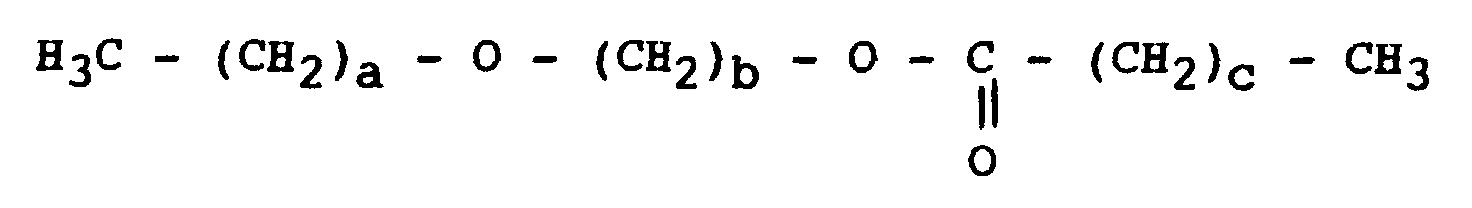
Nach dem bildmäßigen Bestrahlen wird mit geeigneten Entwicklermedien
entwickelt. Als Entwickler können Systeme auf
Basis von Alkylglycol-alkylether-alkylmonocarbonsäure-ester der
allgemeinen Formel
Das erfindungsgemäß Verfahren hat folgende Vorteile:
- Das eingesetzte Polymer ist mikrostrukturierbar; das Polymer ermöglicht die Herstellung von Mikrostrukturen bis hinab zu einer Strukturbreite von wenigen Mikrometern bei gleichzeitig hohem Aspektverhältnis (Verhältnis von Strukturhöhe zu Strukturbreite) von 5 : 1 bis 1000 : 1, vorzugsweise von 10 : 1 bis 100 : 1.
- Mit den angegebenen Epoxidlacken werden bei gleichem Bestrahlungsaufwand Mikrostrukturen mit wesentlich größeren Strukturtiefen erhalten als mit bekannten Kunststoffen. Im Vergleich zu Polymethyl-methacrylat (PMMA) liegt eine Steigerung der Empfindlichkeit um einen Faktor 100 bis 1000 vor.
- Es lassen sich Strukturen mit Strukturhöhen von zum Beispiel 500 µm bei lateralen Abmessungen im Submikrometer-Bereich herstellen, die keine Defekte aufweisen.
- Es ermöglicht, Strukturgenauigkeiten im Submikrometerbereich zu erzielen.
- Die Mikrostrukturen haben scharfe, steile Kanten und glatte Wände.
- Das Polymer ist bis 80 °C mechanisch stabil und hat eine ausreichende thermomechanische Festigkeit.
- Das Polymer übersteht Galvanikprozesse problemlos und ist beständig gegen zum Beispiel saure Kupfer- und Nickelbäder, Schwefelsäure und Amidoschwefelsäure sowie Komplexbildner. Bei Temperaturen zwischen 20 °C und 80 °C bleiben die Mikrostrukturen über 24 Stunden in den Galvanikbädern unverändert.
- Die Oberfläche des Kunststoffs ist glatt; er läßt sich in gleichmäßiger Schichtdicke auf dem Träger auftragen.
- Die angegebenen Entwickler haben eine sehr gute Selektivität.
- Diese Epoxidlacke sind für den LIGA-Prozeß hervorragend geeignet und auf den in der Halbleitertechnik verwendeten Anlagen sehr gut verarbeitbar.
- The polymer used can be microstructured; the polymer enables the production of microstructures down to a structure width of a few micrometers with a high aspect ratio (ratio of structure height to structure width) of 5: 1 to 1000: 1, preferably from 10: 1 to 100: 1.
- With the specified epoxy lacquers, microstructures with significantly greater structure depths are obtained with the same radiation expenditure than with known plastics. Compared to polymethyl methacrylate (PMMA) there is an increase in sensitivity by a factor of 100 to 1000.
- Structures with structural heights of, for example, 500 µm can be produced with lateral dimensions in the submicrometer range, which have no defects.
- It enables structural accuracy to be achieved in the submicrometer range.
- The microstructures have sharp, steep edges and smooth walls.
- The polymer is mechanically stable up to 80 ° C and has sufficient thermomechanical strength.
- The polymer easily survives electroplating processes and is resistant to, for example, acidic copper and nickel baths, sulfuric acid and amidosulfuric acid as well as complexing agents. At temperatures between 20 ° C and 80 ° C, the microstructures remain unchanged for 24 hours in the electroplating baths.
- The surface of the plastic is smooth; it can be applied to the carrier in a uniform layer thickness.
- The developers given have a very good selectivity.
- These epoxy coatings are ideally suited for the LIGA process and can be processed very well on the systems used in semiconductor technology.
Das erfindungsgemäße Verfahren wird anhand der folgenden Beispiele näher erläutert, ohne darauf beschränkt zu sein.The process according to the invention is illustrated by the following examples explained in more detail without being limited thereto.
Auf einen Träger mit den Abmessungen 100 mm Durchmesser und 0,5 mm Dicke aus Silizium (Wafer) wurde durch Spincoaten eine Schicht Epoxidlack SU8 von (505 ± 25) µm Schichtdicke aufgetragen. Dieser Resist wurde auf einer Hotplate bei 90 °C getrocknet und danach an einem Synchrotron mit 2,3 GeV Elektronen-Energie 35 Minuten bei einem mittleren Fingstrom von 20 mA und einem Scannerhub von 20 mm bei einer Scannergeschwindigkeit von 1 mm/s durch eine Röntgenmaske mit Teststrukturen (Felder mit sechskantigen Säulen von 1 µm bis 500 µm Durchmesser) bildmäßig bestrahlt. Die Entwicklung fand bei 25 °C mit PGMEA in 25 Minuten statt. Die Struktur war vollständig frei entwickelt. Der strukturierte Epoxidlack ist an typischen Strukturen völlig frei von Entwicklungsresten und zeigt eine hervorragende Entwickelbarkeit von Einzelsäulen bis in den Bereich von 5 µm (Schlüsselweite).On a carrier with the dimensions 100 mm diameter and A 0.5 mm thick silicon (wafer) was made by spin coating Layer of epoxy paint SU8 of (505 ± 25) µm layer thickness applied. This resist was on a hotplate at 90 ° C dried and then on a synchrotron with 2.3 GeV Electron energy 35 minutes with an average finger current of 20 mA and a scanner stroke of 20 mm at a scanner speed of 1 mm / s through an X-ray mask with test structures (Fields with hexagonal columns from 1 µm to 500 µm Diameter) irradiated imagewise. The development took place at 25 ° C with PGMEA in 25 minutes. The structure was complete freely developed. The structured epoxy paint is typical Structures completely free of development residues and shows one Excellent developability from single columns to the area of 5 µm (width across flats).
Vergleichsbeispiel 1: Ein Probekörper aus PMMA wurde unter den entsprechenden Bedingungen 60 Minuten bestrahlt und mit dem für PMMA optimierten Entwickler (GG-Entwickler) entwickelt. Der Abtrag betrug nur 100 µm. Bei den entsprechenden Säulenstrukturen war maximal die Säule mit einem Durchmesser von 50 µm vorhanden. Säulen mit kleinerem Durchmesser waren verbogen oder zerstört. Comparative Example 1: A test specimen made of PMMA was irradiated under the appropriate conditions for 60 minutes and developed with the developer (GG developer) optimized for PMMA. The removal was only 100 µm. With the corresponding column structures, the maximum column size was 50 µm. Smaller diameter columns were bent or destroyed.
Wie der Vergleich dieser beiden Beispiele zeigt, müssen Strukturhöhen von etwa 500 µm bei PMMA unter gleichen Bedingungen mindestens 10 Stunden bestrahlt werden. Hierbei sind Aspektverhältnisse bis zu 40 erreichbar. Bei SU8 dagegen lassen sich dickere Strukturen bei kürzerer Bestrahlungszeit mit höherem Aspektverhältnis wirtschaftlicher und gleichzeitig mit höherer Qualität herstellen.As the comparison of these two examples shows, must Structural heights of around 500 µm with PMMA under the same conditions be irradiated for at least 10 hours. Here are Aspect ratios up to 40 achievable. Leave it at SU8 thicker structures with shorter exposure times higher aspect ratio more economical and at the same time with produce higher quality.
Auf eine Trägerplatte aus Kupfer wurde der Epoxidlack ELPEMER SD 2054 mit einer Dicke von 300 µm durch Spincoaten aufgebracht und an einem Synchrotron mit 2,3 GeV Elektronen-Energie 15 Minuten bei einem mittleren Ringstrom von 20 mA und einem Scannerhub von 20 mm durch eine Röntgenmaske mit Spektrometerstrukturen bildmäßig bestrahlt. Zur nachfolgenden Entwicklung wurde eine fünfprozentige Lösung von Natriumhydroxid in 1 : 1 Wasser/Glykol bei 25 °C und 75 Minuten eingesetzt. Die Struktur war vollständig frei entwickelt. Das strukturierte Epoxid zeigt an den typischen Gitterzähnen der Spektrometerstruktur eine hervorragende Abbildung der funktionsbestimmenden Zahnkanten. Das Spektrometer ist frei von singulären und statistischen Fehlstellen.The epoxy paint ELPEMER was applied to a copper carrier plate SD 2054 with a thickness of 300 µm applied by spin coating and on a synchrotron with 2.3 GeV electron energy 15 Minutes with an average ring current of 20 mA and a Scanner stroke of 20 mm through an X-ray mask with spectrometer structures irradiated imagewise. To the subsequent development was a five percent solution of sodium hydroxide in 1: 1 water / glycol used at 25 ° C and 75 minutes. The The structure was completely free. The structured Epoxy shows the typical grid teeth of the spectrometer structure an excellent illustration of the function determining Tooth edges. The spectrometer is free of singular and statistical defects.
Vergleichsbeispiel 2: Ein Probekörper aus PMMA auf Kupfer mit einer Schichtdicke von 300 µm wurde unter den gleichen Bedingungen bestrahlt, bis eine PMMA-typische Bestrahldosis für 300 µm eingelagert wurde. Die Bestrahlzeit betrug 6 Stunden. Die Entwicklung erfolgte mit GG-Entwickler. Bei den Zähnen ergab sich ein Dunkelabtrag sowie eine Verrundung der Strukturen über die ganze Zahnhöhe. Die so erzeugte Struktur weist singuläre und statistische Fehlstellen auf. Comparative Example 2: A test specimen made of PMMA on copper with a layer thickness of 300 μm was irradiated under the same conditions until a radiation dose typical for PMMA for 300 μm was stored. The irradiation time was 6 hours. The development was carried out with GG developers. With the teeth, there was a dark erosion and a rounding of the structures over the entire tooth height. The structure created in this way has singular and statistical defects.
Wie der Vergleich dieser beiden Beispiel zeigt, kann die vorgegebene Gitterstruktur für ein Mikrospektrometer mit den typischen Gitterzähnen mit PMMA realisiert werden, wenn erfahrungsgemäß die Mikrostruktur unter 150 µm dick ist. Bei SD 2054 dagegen kann die zu bestrahlende Schicht dicker sein; trotzdem entsteht bei deutlich kürzerer Bestrahlungszeit eine Gitterstruktur mit einwandfreier Zahnform.As the comparison of these two examples shows, the default Grid structure for a microspectrometer with the typical Lattice teeth can be realized with PMMA if experience has shown the microstructure is less than 150 µm thick. With SD 2054 on the other hand, the layer to be irradiated can be thicker; Nevertheless arises with a significantly shorter irradiation time Lattice structure with perfect tooth shape.
Claims (9)
Applications Claiming Priority (2)
| Application Number | Priority Date | Filing Date | Title |
|---|---|---|---|
| DE19741492A DE19741492A1 (en) | 1997-09-19 | 1997-09-19 | Process for the production of microstructure bodies |
| DE19741492 | 1997-09-19 |
Publications (2)
| Publication Number | Publication Date |
|---|---|
| EP0903638A1 true EP0903638A1 (en) | 1999-03-24 |
| EP0903638B1 EP0903638B1 (en) | 2002-09-18 |
Family
ID=7843022
Family Applications (1)
| Application Number | Title | Priority Date | Filing Date |
|---|---|---|---|
| EP98115393A Expired - Lifetime EP0903638B1 (en) | 1997-09-19 | 1998-08-17 | Process for manufacturing microstructured bodies |
Country Status (9)
| Country | Link |
|---|---|
| US (1) | US6251567B1 (en) |
| EP (1) | EP0903638B1 (en) |
| JP (1) | JPH11160871A (en) |
| KR (1) | KR19990029914A (en) |
| CN (1) | CN1145846C (en) |
| AT (1) | ATE224553T1 (en) |
| CA (1) | CA2247777C (en) |
| DE (2) | DE19741492A1 (en) |
| TW (1) | TW515932B (en) |
Cited By (6)
| Publication number | Priority date | Publication date | Assignee | Title |
|---|---|---|---|---|
| EP1035910A1 (en) * | 1997-10-09 | 2000-09-20 | Caliper Technologies Corporation | Microfluidic systems incorporating varied channel depths |
| WO2000074119A1 (en) * | 1999-05-28 | 2000-12-07 | Mitsubishi Denki Kabushiki Kaisha | X-ray exposure apparatus, x-ray exposing method, x-ray mask, x-ray mirror, synchrotron radiator, synchrotron radiating method, and semiconductor device |
| US6947519B2 (en) | 2000-09-18 | 2005-09-20 | Canon Kabushiki Kaisha | X-ray exposure apparatus and method, semiconductor manufacturing apparatus, and microstructure |
| US8961764B2 (en) | 2010-10-15 | 2015-02-24 | Lockheed Martin Corporation | Micro fluidic optic design |
| US9067207B2 (en) | 2009-06-04 | 2015-06-30 | University Of Virginia Patent Foundation | Optical approach for microfluidic DNA electrophoresis detection |
| US9322054B2 (en) | 2012-02-22 | 2016-04-26 | Lockheed Martin Corporation | Microfluidic cartridge |
Families Citing this family (17)
| Publication number | Priority date | Publication date | Assignee | Title |
|---|---|---|---|---|
| US6764652B2 (en) * | 2001-01-24 | 2004-07-20 | The Regents Of The University Of Michigan | Micromachined device for receiving and retaining at least one liquid droplet, method of making the device and method of using the device |
| EP2390721B1 (en) | 2001-08-01 | 2016-03-23 | THE STATE OF OREGON, acting by and through THE STATE BOARD OF HIGHER EDUCATION on behalf of PORTLAND STATE UNIVERSITY | Method for making patterned polymeric structures, particularly microstructures |
| US6740474B2 (en) * | 2001-11-06 | 2004-05-25 | Eastman Kodak Company | Technique for making deep microstructures in photoresist |
| US7459127B2 (en) * | 2002-02-26 | 2008-12-02 | Siemens Healthcare Diagnostics Inc. | Method and apparatus for precise transfer and manipulation of fluids by centrifugal and/or capillary forces |
| US6858378B1 (en) * | 2002-04-17 | 2005-02-22 | Sandia National Laboratories | Photoimageable composition |
| JP4296062B2 (en) * | 2002-08-30 | 2009-07-15 | 服部 正 | Method for manufacturing pattern forming mold |
| US7094354B2 (en) * | 2002-12-19 | 2006-08-22 | Bayer Healthcare Llc | Method and apparatus for separation of particles in a microfluidic device |
| US6916090B2 (en) * | 2003-03-10 | 2005-07-12 | Hewlett-Packard Development Company, L.P. | Integrated fluid ejection device and filter |
| JP3892407B2 (en) * | 2003-03-25 | 2007-03-14 | 富士通株式会社 | Imaging device |
| US7435381B2 (en) * | 2003-05-29 | 2008-10-14 | Siemens Healthcare Diagnostics Inc. | Packaging of microfluidic devices |
| US20040265171A1 (en) * | 2003-06-27 | 2004-12-30 | Pugia Michael J. | Method for uniform application of fluid into a reactive reagent area |
| US20040265172A1 (en) * | 2003-06-27 | 2004-12-30 | Pugia Michael J. | Method and apparatus for entry and storage of specimens into a microfluidic device |
| US20080257754A1 (en) * | 2003-06-27 | 2008-10-23 | Pugia Michael J | Method and apparatus for entry of specimens into a microfluidic device |
| US7347617B2 (en) * | 2003-08-19 | 2008-03-25 | Siemens Healthcare Diagnostics Inc. | Mixing in microfluidic devices |
| US7282324B2 (en) | 2004-01-05 | 2007-10-16 | Microchem Corp. | Photoresist compositions, hardened forms thereof, hardened patterns thereof and metal patterns formed using them |
| GB0419990D0 (en) * | 2004-09-09 | 2004-10-13 | Suisse Electronique Microtech | Marking articles |
| US8148055B2 (en) * | 2006-06-30 | 2012-04-03 | Infineon Technologies Ag | Method for developing a photoresist |
Citations (6)
| Publication number | Priority date | Publication date | Assignee | Title |
|---|---|---|---|---|
| US4756989A (en) * | 1984-07-11 | 1988-07-12 | Asahi Kasei Kogyo Kabushiki Kaisha | Image-forming materials sensitive to high-energy beam |
| EP0375929A2 (en) * | 1988-12-30 | 1990-07-04 | International Business Machines Corporation | Method for patterning cationic curable photoresist |
| US5153898A (en) * | 1986-07-11 | 1992-10-06 | Canon Kabushiki Kaisha | X-ray reduction projection exposure system of reflection type |
| EP0547419A1 (en) * | 1991-12-14 | 1993-06-23 | BASF Aktiengesellschaft | Process for making microstructures |
| US5415977A (en) * | 1991-03-12 | 1995-05-16 | Basf Aktiengesellschaft | Production of micromoldings having a high aspect ratio |
| EP0851295A1 (en) * | 1996-12-27 | 1998-07-01 | Ecole Polytechnique Federale De Lausanne | Process for the fabrication of microstructures by multilayer conformation of a photosensitive resin et microstructures obtained therewith |
-
1997
- 1997-09-19 DE DE19741492A patent/DE19741492A1/en not_active Withdrawn
-
1998
- 1998-08-17 EP EP98115393A patent/EP0903638B1/en not_active Expired - Lifetime
- 1998-08-17 AT AT98115393T patent/ATE224553T1/en not_active IP Right Cessation
- 1998-08-17 DE DE59805591T patent/DE59805591D1/en not_active Expired - Lifetime
- 1998-09-17 TW TW087115454A patent/TW515932B/en active
- 1998-09-18 KR KR1019980038606A patent/KR19990029914A/en active IP Right Grant
- 1998-09-18 CA CA2247777A patent/CA2247777C/en not_active Expired - Fee Related
- 1998-09-18 CN CNB981195032A patent/CN1145846C/en not_active Expired - Fee Related
- 1998-09-18 JP JP10264934A patent/JPH11160871A/en active Pending
- 1998-09-21 US US09/157,518 patent/US6251567B1/en not_active Expired - Fee Related
Patent Citations (6)
| Publication number | Priority date | Publication date | Assignee | Title |
|---|---|---|---|---|
| US4756989A (en) * | 1984-07-11 | 1988-07-12 | Asahi Kasei Kogyo Kabushiki Kaisha | Image-forming materials sensitive to high-energy beam |
| US5153898A (en) * | 1986-07-11 | 1992-10-06 | Canon Kabushiki Kaisha | X-ray reduction projection exposure system of reflection type |
| EP0375929A2 (en) * | 1988-12-30 | 1990-07-04 | International Business Machines Corporation | Method for patterning cationic curable photoresist |
| US5415977A (en) * | 1991-03-12 | 1995-05-16 | Basf Aktiengesellschaft | Production of micromoldings having a high aspect ratio |
| EP0547419A1 (en) * | 1991-12-14 | 1993-06-23 | BASF Aktiengesellschaft | Process for making microstructures |
| EP0851295A1 (en) * | 1996-12-27 | 1998-07-01 | Ecole Polytechnique Federale De Lausanne | Process for the fabrication of microstructures by multilayer conformation of a photosensitive resin et microstructures obtained therewith |
Non-Patent Citations (3)
| Title |
|---|
| H. LORENZ ET AL.: "Mechanical Characterization of a New High-Aspect-Ratio Near UV-Photorsist", MICROELECTRONIC ENGINEERING, vol. 41/42, 1998, pages 371- - 374, XP004111658 * |
| H.LORENZ ET AL.: "High-aspect-ratio, ultrathick, negative-tone photoresist and its application for MEMS", SNSORS AND ACTUATORS A, vol. 64, no. 1, 1998, pages 33 - 39, XP004102135 * |
| Y. ZHAANG ET AL.: "IGH aspect ratio micromachining Teflon by direct exposure to synchrotron radiation", APPL.PHYS. LETT., vol. 67, no. 6, 7 August 1995 (1995-08-07), pages 872 - 874, XP000674181 * |
Cited By (12)
| Publication number | Priority date | Publication date | Assignee | Title |
|---|---|---|---|---|
| EP1035910A1 (en) * | 1997-10-09 | 2000-09-20 | Caliper Technologies Corporation | Microfluidic systems incorporating varied channel depths |
| EP1035910A4 (en) * | 1997-10-09 | 2002-07-31 | Caliper Techn Corp | Microfluidic systems incorporating varied channel depths |
| US6517234B1 (en) | 1997-10-09 | 2003-02-11 | Caliper Technologies Corp. | Microfluidic systems incorporating varied channel dimensions |
| WO2000074119A1 (en) * | 1999-05-28 | 2000-12-07 | Mitsubishi Denki Kabushiki Kaisha | X-ray exposure apparatus, x-ray exposing method, x-ray mask, x-ray mirror, synchrotron radiator, synchrotron radiating method, and semiconductor device |
| US6947518B2 (en) | 1999-05-28 | 2005-09-20 | Mitsubishi Denki Kabushiki Kaisha | X-ray exposure apparatus, X-ray exposure method, X-ray mask, X-ray mirror, synchrotron radiation apparatus, synchrotron radiation method and semiconductor device |
| US6947519B2 (en) | 2000-09-18 | 2005-09-20 | Canon Kabushiki Kaisha | X-ray exposure apparatus and method, semiconductor manufacturing apparatus, and microstructure |
| US9067207B2 (en) | 2009-06-04 | 2015-06-30 | University Of Virginia Patent Foundation | Optical approach for microfluidic DNA electrophoresis detection |
| US9649631B2 (en) | 2009-06-04 | 2017-05-16 | Leidos Innovations Technology, Inc. | Multiple-sample microfluidic chip for DNA analysis |
| US9656261B2 (en) | 2009-06-04 | 2017-05-23 | Leidos Innovations Technology, Inc. | DNA analyzer |
| US8961764B2 (en) | 2010-10-15 | 2015-02-24 | Lockheed Martin Corporation | Micro fluidic optic design |
| US9322054B2 (en) | 2012-02-22 | 2016-04-26 | Lockheed Martin Corporation | Microfluidic cartridge |
| US9988676B2 (en) | 2012-02-22 | 2018-06-05 | Leidos Innovations Technology, Inc. | Microfluidic cartridge |
Also Published As
| Publication number | Publication date |
|---|---|
| CN1212382A (en) | 1999-03-31 |
| US6251567B1 (en) | 2001-06-26 |
| JPH11160871A (en) | 1999-06-18 |
| DE19741492A1 (en) | 1999-03-25 |
| CA2247777C (en) | 2010-06-29 |
| CN1145846C (en) | 2004-04-14 |
| EP0903638B1 (en) | 2002-09-18 |
| ATE224553T1 (en) | 2002-10-15 |
| DE59805591D1 (en) | 2002-10-24 |
| TW515932B (en) | 2003-01-01 |
| CA2247777A1 (en) | 1999-03-19 |
| KR19990029914A (en) | 1999-04-26 |
Similar Documents
| Publication | Publication Date | Title |
|---|---|---|
| EP0903638B1 (en) | Process for manufacturing microstructured bodies | |
| DE4024275C2 (en) | ||
| DE2655455C2 (en) | Method for producing a mask and lacquer structure for use in the method | |
| DE3930087A1 (en) | POSITIVELY WORKING RADIATION-SENSITIVE MIXTURE AND PRODUCTION OF RADIATION-SENSITIVE RECORDING MATERIAL THEREOF | |
| EP0051166A1 (en) | Process for the stress-free development of irradiated polymethylmethacrylate layers | |
| EP0141389A2 (en) | Process for the production of image-wise structured resists, and dry resist therefor | |
| EP0019122A2 (en) | Process for the phototechnical production of relief structures | |
| DE3842354C2 (en) | ||
| DE2847764C2 (en) | Photosensitive material and process for forming ultrafine patterns | |
| EP0547419B1 (en) | Process for making microstructures | |
| DE4303923A1 (en) | Process for removing plastics from microstructures | |
| DE4234423C2 (en) | Metal or semiconductor substrates coated with a resist and method for achieving stable resist-substrate adhesion | |
| EP0503377A1 (en) | Process for making micro structure having a high aspect ratio | |
| EP0580052A2 (en) | Process for making microstructures | |
| DE4107662A1 (en) | METHOD FOR PRODUCING MICROFORMED BODIES WITH A HIGH ASPECT RATIO | |
| US6682870B1 (en) | Enhanced adhesion for LIGA microfabrication by using a buffer layer | |
| DE102011050722B4 (en) | Method for producing a multilayer structure with a microstructured surface | |
| DE60306682T2 (en) | A HAFTSCHICHT COMPREHENSIVE MICROSTRUCTURE AND METHOD FOR THE PRODUCTION OF SUCH A MICROSTRUCTURE | |
| DE4310976C1 (en) | Vitreous carbon@ used as carrier for x=ray resist material and mask for deep lithography | |
| DE3028308A1 (en) | Integrated semiconductor circuit prodn. - by electron bombardment, UV irradiation and alkali treatment of a phenolic condensation resin having a photosensitive lacquer | |
| Vlnieska | Synthesis and chemical characterization of photoresists for X-ray imaging | |
| DE4229244A1 (en) | Process for the production of microstructure bodies | |
| Fischer et al. | Large area, cost effective X-ray masks for high energy photons | |
| DE4329445A1 (en) | Process for the delamination of microstructures | |
| DD272141A1 (en) | METHOD FOR PRODUCING SILICYL-CONTAINING NEGATIVE RESISTANT IMAGES |
Legal Events
| Date | Code | Title | Description |
|---|---|---|---|
| PUAI | Public reference made under article 153(3) epc to a published international application that has entered the european phase |
Free format text: ORIGINAL CODE: 0009012 |
|
| AK | Designated contracting states |
Kind code of ref document: A1 Designated state(s): AT BE CH DE FR GB IT LI NL |
|
| AX | Request for extension of the european patent |
Free format text: AL;LT;LV;MK;RO;SI |
|
| 17P | Request for examination filed |
Effective date: 19990922 |
|
| AKX | Designation fees paid |
Free format text: AT BE CH DE FR GB IT LI NL |
|
| 17Q | First examination report despatched |
Effective date: 20000526 |
|
| GRAG | Despatch of communication of intention to grant |
Free format text: ORIGINAL CODE: EPIDOS AGRA |
|
| GRAG | Despatch of communication of intention to grant |
Free format text: ORIGINAL CODE: EPIDOS AGRA |
|
| GRAH | Despatch of communication of intention to grant a patent |
Free format text: ORIGINAL CODE: EPIDOS IGRA |
|
| RAP1 | Party data changed (applicant data changed or rights of an application transferred) |
Owner name: STEAG MICROPARTS GMBH |
|
| RIN1 | Information on inventor provided before grant (corrected) |
Inventor name: SPITZNER, ULRIKE Inventor name: SCHAEFERMEIER, BERNHARD Inventor name: BALLHORN, RALPH-ULRICH Inventor name: KAPITZKA, NORBERT Inventor name: REINECKE, HOLGER, DR. |
|
| GRAH | Despatch of communication of intention to grant a patent |
Free format text: ORIGINAL CODE: EPIDOS IGRA |
|
| GRAA | (expected) grant |
Free format text: ORIGINAL CODE: 0009210 |
|
| AK | Designated contracting states |
Kind code of ref document: B1 Designated state(s): AT BE CH DE FR GB IT LI NL |
|
| REF | Corresponds to: |
Ref document number: 224553 Country of ref document: AT Date of ref document: 20021015 Kind code of ref document: T |
|
| REG | Reference to a national code |
Ref country code: GB Ref legal event code: FG4D Free format text: NOT ENGLISH |
|
| REG | Reference to a national code |
Ref country code: CH Ref legal event code: NV Representative=s name: SCHMAUDER & PARTNER AG PATENTANWALTSBUERO Ref country code: CH Ref legal event code: EP |
|
| REF | Corresponds to: |
Ref document number: 59805591 Country of ref document: DE Date of ref document: 20021024 |
|
| GBT | Gb: translation of ep patent filed (gb section 77(6)(a)/1977) |
Effective date: 20021030 |
|
| ET | Fr: translation filed | ||
| PLBE | No opposition filed within time limit |
Free format text: ORIGINAL CODE: 0009261 |
|
| STAA | Information on the status of an ep patent application or granted ep patent |
Free format text: STATUS: NO OPPOSITION FILED WITHIN TIME LIMIT |
|
| 26N | No opposition filed |
Effective date: 20030619 |
|
| REG | Reference to a national code |
Ref country code: CH Ref legal event code: PFA Owner name: BOEHRINGER INGELHEIM MICROPARTS GMBH Free format text: STEAG MICROPARTS GMBH#HAUERT 7#44227 DORTMUND (DE) -TRANSFER TO- BOEHRINGER INGELHEIM MICROPARTS GMBH#HAUERT 7#44227 DORTMUND (DE) |
|
| REG | Reference to a national code |
Ref country code: FR Ref legal event code: CD |
|
| REG | Reference to a national code |
Ref country code: CH Ref legal event code: PCAR Free format text: SCHMAUDER & PARTNER AG PATENT- UND MARKENANWAELTE VSP;ZWAENGIWEG 7;8038 ZUERICH (CH) |
|
| PGFP | Annual fee paid to national office [announced via postgrant information from national office to epo] |
Ref country code: NL Payment date: 20090814 Year of fee payment: 12 Ref country code: GB Payment date: 20090827 Year of fee payment: 12 Ref country code: DE Payment date: 20090821 Year of fee payment: 12 Ref country code: CH Payment date: 20090825 Year of fee payment: 12 Ref country code: AT Payment date: 20090814 Year of fee payment: 12 |
|
| PGFP | Annual fee paid to national office [announced via postgrant information from national office to epo] |
Ref country code: BE Payment date: 20090915 Year of fee payment: 12 |
|
| PGFP | Annual fee paid to national office [announced via postgrant information from national office to epo] |
Ref country code: IT Payment date: 20090821 Year of fee payment: 12 |
|
| BERE | Be: lapsed |
Owner name: *STEAG MICROPARTS G.M.B.H. Effective date: 20100831 |
|
| REG | Reference to a national code |
Ref country code: NL Ref legal event code: V1 Effective date: 20110301 |
|
| REG | Reference to a national code |
Ref country code: CH Ref legal event code: PL |
|
| GBPC | Gb: european patent ceased through non-payment of renewal fee |
Effective date: 20100817 |
|
| PG25 | Lapsed in a contracting state [announced via postgrant information from national office to epo] |
Ref country code: LI Free format text: LAPSE BECAUSE OF NON-PAYMENT OF DUE FEES Effective date: 20100831 Ref country code: CH Free format text: LAPSE BECAUSE OF NON-PAYMENT OF DUE FEES Effective date: 20100831 |
|
| REG | Reference to a national code |
Ref country code: FR Ref legal event code: ST Effective date: 20110502 |
|
| PG25 | Lapsed in a contracting state [announced via postgrant information from national office to epo] |
Ref country code: AT Free format text: LAPSE BECAUSE OF NON-PAYMENT OF DUE FEES Effective date: 20100817 Ref country code: IT Free format text: LAPSE BECAUSE OF NON-PAYMENT OF DUE FEES Effective date: 20100817 Ref country code: NL Free format text: LAPSE BECAUSE OF NON-PAYMENT OF DUE FEES Effective date: 20110301 |
|
| REG | Reference to a national code |
Ref country code: DE Ref legal event code: R119 Ref document number: 59805591 Country of ref document: DE Effective date: 20110301 |
|
| PG25 | Lapsed in a contracting state [announced via postgrant information from national office to epo] |
Ref country code: FR Free format text: LAPSE BECAUSE OF NON-PAYMENT OF DUE FEES Effective date: 20100831 Ref country code: BE Free format text: LAPSE BECAUSE OF NON-PAYMENT OF DUE FEES Effective date: 20100831 Ref country code: DE Free format text: LAPSE BECAUSE OF NON-PAYMENT OF DUE FEES Effective date: 20110301 |
|
| PG25 | Lapsed in a contracting state [announced via postgrant information from national office to epo] |
Ref country code: GB Free format text: LAPSE BECAUSE OF NON-PAYMENT OF DUE FEES Effective date: 20100817 |
|
| PGFP | Annual fee paid to national office [announced via postgrant information from national office to epo] |
Ref country code: FR Payment date: 20090914 Year of fee payment: 12 |