EP0901182A2 - GPS wave antenna apparatus - Google Patents
GPS wave antenna apparatus Download PDFInfo
- Publication number
- EP0901182A2 EP0901182A2 EP98306947A EP98306947A EP0901182A2 EP 0901182 A2 EP0901182 A2 EP 0901182A2 EP 98306947 A EP98306947 A EP 98306947A EP 98306947 A EP98306947 A EP 98306947A EP 0901182 A2 EP0901182 A2 EP 0901182A2
- Authority
- EP
- European Patent Office
- Prior art keywords
- gps wave
- antenna element
- wave antenna
- antenna apparatus
- gps
- Prior art date
- Legal status (The legal status is an assumption and is not a legal conclusion. Google has not performed a legal analysis and makes no representation as to the accuracy of the status listed.)
- Withdrawn
Links
Images


Classifications
-
- H—ELECTRICITY
- H01—ELECTRIC ELEMENTS
- H01Q—ANTENNAS, i.e. RADIO AERIALS
- H01Q23/00—Antennas with active circuits or circuit elements integrated within them or attached to them
-
- G—PHYSICS
- G01—MEASURING; TESTING
- G01S—RADIO DIRECTION-FINDING; RADIO NAVIGATION; DETERMINING DISTANCE OR VELOCITY BY USE OF RADIO WAVES; LOCATING OR PRESENCE-DETECTING BY USE OF THE REFLECTION OR RERADIATION OF RADIO WAVES; ANALOGOUS ARRANGEMENTS USING OTHER WAVES
- G01S19/00—Satellite radio beacon positioning systems; Determining position, velocity or attitude using signals transmitted by such systems
- G01S19/01—Satellite radio beacon positioning systems transmitting time-stamped messages, e.g. GPS [Global Positioning System], GLONASS [Global Orbiting Navigation Satellite System] or GALILEO
- G01S19/13—Receivers
- G01S19/35—Constructional details or hardware or software details of the signal processing chain
- G01S19/36—Constructional details or hardware or software details of the signal processing chain relating to the receiver frond end
-
- H—ELECTRICITY
- H01—ELECTRIC ELEMENTS
- H01Q—ANTENNAS, i.e. RADIO AERIALS
- H01Q1/00—Details of, or arrangements associated with, antennas
- H01Q1/12—Supports; Mounting means
- H01Q1/22—Supports; Mounting means by structural association with other equipment or articles
-
- H—ELECTRICITY
- H01—ELECTRIC ELEMENTS
- H01Q—ANTENNAS, i.e. RADIO AERIALS
- H01Q1/00—Details of, or arrangements associated with, antennas
- H01Q1/36—Structural form of radiating elements, e.g. cone, spiral, umbrella; Particular materials used therewith
- H01Q1/38—Structural form of radiating elements, e.g. cone, spiral, umbrella; Particular materials used therewith formed by a conductive layer on an insulating support
-
- H—ELECTRICITY
- H01—ELECTRIC ELEMENTS
- H01Q—ANTENNAS, i.e. RADIO AERIALS
- H01Q7/00—Loop antennas with a substantially uniform current distribution around the loop and having a directional radiation pattern in a plane perpendicular to the plane of the loop
Definitions
- the present invention relates to a GPS (Global Positioning System) wave antenna apparatus mounted on part of an automobile and the like.
- GPS Global Positioning System
- an antenna element of thin-plate conductor is formed on the surface of a dielectric block made of ceramics and the like as a patch antenna, and this patch antenna is placed on the surface of a printed circuit board.
- an LNA Low Noise Amplifier
- a transistor, a resistor and a capacitor is mounted on the back of the printed circuit board.
- a ground plate is generally formed on the back of the antenna.
- the GPS wave antenna apparatus having the above constitution causes the following problem. Since the printed circuit board is bonded to the patch antenna having a considerably great thickness, the total thickness of the antenna apparatus is increased. Since, furthermore, the ground plate is mounted on the back of the patch antenna, the thickness of the antenna apparatus is increased greater or greater. Since the antenna apparatus has a three-layered structure of the patch antenna, printed circuit board and ground plate, its structure is considerably complicated, its manufacture is difficult, and its manufacturing cost is high.
- An object of the present invention is to provide a GPS wave antenna apparatus which is not only capable of receiving a GPS wave satisfactorily, but also simple in constitution, low in manufacturing costs, and easy to maintain and control.
- the GPS wave antenna apparatus of the present invention has the following constitution.
- the characteristic constitution other than the above will be clarified in the embodiment of the present invention.
- a GPS wave antenna apparatus comprising a substrate unit having a printed board on which an antenna constituting element including a GPS wave antenna element is mounted integrally as one component, a case having an opening portion at one end, for detachably receiving the substrate unit through the opening portion, and a conductive plate attached to the case so as to block the opening portion and arranged opposite to the GPS wave antenna element at a fixed distance therebetween.
- an antenna constituting element including a GPS wave antenna element having a thin-film conductive pattern is formed on a single printed board integrally with each other as one component to be constituted as a substrate unit.
- the antenna apparatus is therefore capable of receiving a GPS wave satisfactorily and made compact greatly.
- the antenna apparatus has a two-layered structure of a substrate unit and a conductive plate; however, since the conductive plate is used as a lid for blocking an opening portion of a case, the antenna apparatus is substantially constituted of a single layer. Consequently, the apparatus is easy in constitution and low in manufacturing costs. Since, moreover, the apparatus is easy to assemble and disassemble, its maintenance and control can be performed very satisfactorily.
- reference numeral 10 indicates a substrate unit
- numeral 20 shows a case
- numeral 30 denotes a conductive plate.
- the substrate unit 10 has a printed board 11 on which an antenna constituting element including a GPS wave antenna element 12 is mounted integrally as one component. More specifically, the antenna element 12 has a thin-film conductive pattern P and is formed on the surface of the printed board 11, and the substrate unit 10 includes a low noise amplifier 13 provided near a corner portion of the back of the printed board 11, and a feeder 14 constituted of a coaxial cable one end of which is connected to a feeder section of the antenna element 12 through the low noise amplifier 13.
- One end of the low noise amplifier 13 is electrically connected to the feeder section of the antenna element 12, and the other end thereof is electrically connected to a conductive portion of the feeder 14.
- a connector 15 is attached to the tip of the feeder 14.
- the thin-film conductive pattern P of the antenna element 12 is formed of a compound line including thin, narrow conductive lines (e.g., copper-made strip conductive lines) arranged in parallel and an almost rectangular conductive loop including a short side of the compound line, thereby constituting a right-hand circular polarization antenna element.
- the antenna element 12 is so formed that it radiates circularly polarized wave in a direction perpendicular to the plane on which the rectangular loop is formed.
- Arc-shaped cutaway portions a1, a2, a3 and a4, which are to be guided and fitted to the mounting columns of the case 20 (described later), are provided at four corners of the printed board.
- the case 20 is integrally molded by ABS resin so as to be shaped like a box, and its one end serves as an opening portion 21 capable of detachably receiving the substrate unit 10.
- a feeder lead-through hole 22 is provided at part of the wall of the case 20, and the mounting columns b1, b2, b3 and b4 are provided at four corners of the inner surface of the case 20.
- the outer surfaces of these mounting columns b1 to b4 serve to guide the arc-shaped cutaway portions al to a4 formed at the four corners of the printed board.
- the conductive plate 30 is constituted of a rectangular aluminum plate having a thickness of about 2 mm and has screw insertion holes c1, c2, c3 and c4 at four corners thereof. These screw insertion holes c1 to c4 correspond to screw holes of the mounting columns b1 to b4.
- the conductive plate 30 is mounted on the case 20 as a lid for blocking the opening portion 21 of the case 20. Thus, the conductive plate 30 is arranged opposite to the GPS wave antenna element 12 at a fixed distance between them. Since the conductive plate 30 is so arranged, even when the antenna is mounted on an automobile, the influence of diffused reflection due to peripheral metal members can be eliminated, and the antenna characteristics can be prevented from deteriorating.
- the substrate unit 10 is inserted into a hollow of the case 20 through the opening portion 21 thereof. Since, in this case, the arc-shaped cutaway portions a1 to a4 at the four corners of the substrate unit 10 are slidably fitted on the outer surfaces of the mounting columns b1 to b4, the unit 10 can be smoothly inserted using the columns b1 to b4 as a guide.
- a spacer is interposed between the unit 10 and each of the columns b1 to b4, as indicated by broken line X, and then the conductive plate 30 is brought into contact with the opening portion 21 of the case 20 as a lid.
- a screw (not shown) is inserted into the screw hole of each of the columns b1 to b4 through a corresponding one of the screw insertion holes c1 to c4. The antenna apparatus can thus be easily assembled.
- the antenna apparatus can easily be disassembled by reversing the above procedure, its maintenance is easy to perform.
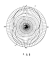
- FIG. 3 is a view of experimental result of directivity of the antenna apparatus according to the embodiment of the present invention, showing a vertical plane radiation pattern which is formed in a direction perpendicular to thin-film conductive pattern P when the substrate unit 10 is arranged horizontally.
- solid curved line A indicates the characteristics of a discrete antenna excluding the conductive plate 30 (substrate unit 10 only), and broken curved line B does the characteristics of the antenna including the conductive plate 30.
- the GPS wave antenna apparatus can be modified as follows:
Abstract
Description
- The present invention relates to a GPS (Global Positioning System) wave antenna apparatus mounted on part of an automobile and the like.
- In a conventionally-known GPS wave antenna apparatus, an antenna element of thin-plate conductor is formed on the surface of a dielectric block made of ceramics and the like as a patch antenna, and this patch antenna is placed on the surface of a printed circuit board. In most cases, an LNA (Low Noise Amplifier) including a transistor, a resistor and a capacitor is mounted on the back of the printed circuit board. For the above antenna using a dielectric, a ground plate is generally formed on the back of the antenna.
- The GPS wave antenna apparatus having the above constitution causes the following problem. Since the printed circuit board is bonded to the patch antenna having a considerably great thickness, the total thickness of the antenna apparatus is increased. Since, furthermore, the ground plate is mounted on the back of the patch antenna, the thickness of the antenna apparatus is increased greater or greater. Since the antenna apparatus has a three-layered structure of the patch antenna, printed circuit board and ground plate, its structure is considerably complicated, its manufacture is difficult, and its manufacturing cost is high.
- An object of the present invention is to provide a GPS wave antenna apparatus which is not only capable of receiving a GPS wave satisfactorily, but also simple in constitution, low in manufacturing costs, and easy to maintain and control.
- To attain the above object, the GPS wave antenna apparatus of the present invention has the following constitution. The characteristic constitution other than the above will be clarified in the embodiment of the present invention.
- According to an aspect of the present invention, there is provided a GPS wave antenna apparatus comprising a substrate unit having a printed board on which an antenna constituting element including a GPS wave antenna element is mounted integrally as one component, a case having an opening portion at one end, for detachably receiving the substrate unit through the opening portion, and a conductive plate attached to the case so as to block the opening portion and arranged opposite to the GPS wave antenna element at a fixed distance therebetween.
- In the GPS wave antenna apparatus having the above constitution, an antenna constituting element including a GPS wave antenna element having a thin-film conductive pattern is formed on a single printed board integrally with each other as one component to be constituted as a substrate unit. The antenna apparatus is therefore capable of receiving a GPS wave satisfactorily and made compact greatly. The antenna apparatus has a two-layered structure of a substrate unit and a conductive plate; however, since the conductive plate is used as a lid for blocking an opening portion of a case, the antenna apparatus is substantially constituted of a single layer. Consequently, the apparatus is easy in constitution and low in manufacturing costs. Since, moreover, the apparatus is easy to assemble and disassemble, its maintenance and control can be performed very satisfactorily.
- This summary of the invention does not necessarily describe all necessary features so that the invention may also be a sub-combination of these described features.
- The invention can be more fully under stood from the following detailed description when taken in conjunction with the accompanying drawings, in which:
- FIG. 1 is a cutaway, perspective view of the constitution of a GPS wave antenna apparatus according to an embodiment of the present invention;
- FIG. 2 is an exploded, perspective view depicting the GPS wave antenna apparatus of FIG. 1 top side down; and
- FIG. 3 is a view of a vertical plane radiation pattern showing experimental results of directivity of the GPS wave antenna apparatus according to the embodiment of the present invention.
-
- In FIGS. 1 and 2,
reference numeral 10 indicates a substrate unit,numeral 20 shows a case, andnumeral 30 denotes a conductive plate. - The
substrate unit 10 has a printedboard 11 on which an antenna constituting element including a GPSwave antenna element 12 is mounted integrally as one component. More specifically, theantenna element 12 has a thin-film conductive pattern P and is formed on the surface of the printedboard 11, and thesubstrate unit 10 includes alow noise amplifier 13 provided near a corner portion of the back of the printedboard 11, and afeeder 14 constituted of a coaxial cable one end of which is connected to a feeder section of theantenna element 12 through thelow noise amplifier 13. - One end of the
low noise amplifier 13 is electrically connected to the feeder section of theantenna element 12, and the other end thereof is electrically connected to a conductive portion of thefeeder 14. Aconnector 15 is attached to the tip of thefeeder 14. - The thin-film conductive pattern P of the
antenna element 12 is formed of a compound line including thin, narrow conductive lines (e.g., copper-made strip conductive lines) arranged in parallel and an almost rectangular conductive loop including a short side of the compound line, thereby constituting a right-hand circular polarization antenna element. Theantenna element 12 is so formed that it radiates circularly polarized wave in a direction perpendicular to the plane on which the rectangular loop is formed. - Arc-shaped cutaway portions a1, a2, a3 and a4, which are to be guided and fitted to the mounting columns of the case 20 (described later), are provided at four corners of the printed board.
- The
case 20 is integrally molded by ABS resin so as to be shaped like a box, and its one end serves as anopening portion 21 capable of detachably receiving thesubstrate unit 10. A feeder lead-throughhole 22 is provided at part of the wall of thecase 20, and the mounting columns b1, b2, b3 and b4 are provided at four corners of the inner surface of thecase 20. The outer surfaces of these mounting columns b1 to b4 serve to guide the arc-shaped cutaway portions al to a4 formed at the four corners of the printed board. - The
conductive plate 30 is constituted of a rectangular aluminum plate having a thickness of about 2 mm and has screw insertion holes c1, c2, c3 and c4 at four corners thereof. These screw insertion holes c1 to c4 correspond to screw holes of the mounting columns b1 to b4. Theconductive plate 30 is mounted on thecase 20 as a lid for blocking theopening portion 21 of thecase 20. Thus, theconductive plate 30 is arranged opposite to the GPSwave antenna element 12 at a fixed distance between them. Since theconductive plate 30 is so arranged, even when the antenna is mounted on an automobile, the influence of diffused reflection due to peripheral metal members can be eliminated, and the antenna characteristics can be prevented from deteriorating. - To fabricate the foregoing antenna apparatus, the
substrate unit 10 is inserted into a hollow of thecase 20 through theopening portion 21 thereof. Since, in this case, the arc-shaped cutaway portions a1 to a4 at the four corners of thesubstrate unit 10 are slidably fitted on the outer surfaces of the mounting columns b1 to b4, theunit 10 can be smoothly inserted using the columns b1 to b4 as a guide. - When the
substrate unit 10 reaches the innermost portion of thecase 20, a spacer is interposed between theunit 10 and each of the columns b1 to b4, as indicated by broken line X, and then theconductive plate 30 is brought into contact with theopening portion 21 of thecase 20 as a lid. A screw (not shown) is inserted into the screw hole of each of the columns b1 to b4 through a corresponding one of the screw insertion holes c1 to c4. The antenna apparatus can thus be easily assembled. - Since, furthermore, the antenna apparatus can easily be disassembled by reversing the above procedure, its maintenance is easy to perform.
- FIG. 3 is a view of experimental result of directivity of the antenna apparatus according to the embodiment of the present invention, showing a vertical plane radiation pattern which is formed in a direction perpendicular to thin-film conductive pattern P when the
substrate unit 10 is arranged horizontally. In FIG. 3, solid curved line A indicates the characteristics of a discrete antenna excluding the conductive plate 30 (substrate unit 10 only), and broken curved line B does the characteristics of the antenna including theconductive plate 30. - As illustrated in FIG. 3, it was confirmed that the directivity of the antenna apparatus was strengthened upward (toward the upper portion of FIG. 3). (Modifications)
- The GPS wave antenna apparatus according to the above embodiment can be modified as follows:
- i) A GPS wave antenna element other than the right-hand circular polarization antenna element can be used.
- ii) The
case 20 can be formed of resin other than ABS resin. - iii) The
conductive plate 30 can be formed of brass, iron or the like as well as aluminum. - iv) The feeder section can be detachably connected to the low noise amplifier.
-
-
- [1] A GPS wave antenna apparatus comprises
a
substrate unit 10 having a printedboard 11 on which an antenna constituting element including a GPSwave antenna element 12 is mounted integrally as one component, acase 20 having anopening portion 21 at one end, for detachably receiving thesubstrate unit 10 through theopening portion 21, and aconductive plate 30 attached to thecase 20 so as to block theopening portion 21 and arranged opposite to the GPSwave antenna element 12 at a fixed distance therebetween. - [2] In the GPS wave antenna apparatus according
to the above item [1], the GPS
wave antenna element 12 has a thin-film conductive pattern, and thesubstrate unit 10 includes alow noise amplifier 13 provided on the printedboard 11 and afeeder 14 connected to a feeder section of theantenna element 12 through thelow noise amplifier 13. - [3] In the GPS wave antenna apparatus according
to the above item [1], the GPS
wave antenna element 12 includes a loop antenna element. - [4] A GPS wave antenna apparatus comprises a GPS
wave
loop antenna element 12 having a thin-film conductive pattern formed on a printedboard 11, asubstrate unit 10 on which a constituting element including theloop antenna element 12 is mounted integrally as one component, alow noise amplifier 13 provided on the printedboard 11, and afeeder 14 connected to a feeder section of theloop antenna element 12 through thelow noise amplifier 13. - [5] The GPS wave antenna apparatus according to
the above item [4] further comprises a
conductive plate 30 arranged opposite to the GPS waveloop antenna element 12 at a fixed distance therebetween. The directivity of the GPS wave antenna apparatus can thus be stabilized. - [6] In the GPS wave antenna apparatus according
to the above item [5], the
conductive plate 30 is arranged under theloop antenna element 12. A GPS wave antenna apparatus requires an upward directivity. The apparatus of the present invention can be prevented from being out of directivity due to an object under the apparatus. - [7] In the GPS wave antenna apparatus according
to the above item [5], the
conductive plate 30 is provided so as to cover an underside of the low noise amplifier. Theconductive plate 30 prevents noise generated from thelow noise amplifier 13 from being transmitted downward. - [8] In the GPS wave antenna apparatus according
to the above item [4], the
loop antenna element 12 is formed on one side of the printedboard 11, and thelow noise amplifier 13 is formed on the other side thereof. The formation of theelement 12 andamplifier 13 improves the layout of the apparatus. - [9] In the GPS wave antenna apparatus according
to the above item [8], the one side of the printed
board 11 on which theloop antenna element 12 is formed, is located in an innermost portion of acase 20. Since theloop antenna element 12 is fixed in thecase 20 stably in such a manner that they are close to each other, the reception characteristics are stabilized. If the other side of the printedboard 11 on which thelow noise amplifier 13 is formed is located in the innermost portion of thecase 20, a gap is caused between thesubstrate 11 andcase 20. Since basically thecase 20 has a dielectric constant, the reception characteristics are varied with a value of the gap. The simple structure of the apparatus of the present invention prevents the reception characteristics from being varied. -
Claims (9)
- A GPS wave antenna apparatus characterized by comprising:a substrate unit (10) having a printed board (11) on which an antenna constituting element including a GPS wave antenna element (12) is mounted integrally as one component;a case (20) having an opening portion (21) at one end, for detachably receiving the substrate unit (10) through the opening portion (21); anda conductive plate (30) attached to the case (20) so as to block the opening portion (21) and arranged opposite to the GPS wave antenna element (12) at a fixed distance therebetween.
- The GPS wave antenna apparatus according to claim 1, characterized in that the GPS wave antenna element (12) has a thin-film conductive pattern, and the substrate unit (10) includes a low noise amplifier (13) provided on the printed board (11) and a feeder (14) connected to a feeder section of the antenna element (12) through the low noise amplifier (13).
- The GPS wave antenna apparatus according to claim 1, characterized in that the GPS wave antenna element (12) includes a loop antenna element.
- A GPS wave antenna apparatus characterized by comprising:a GPS wave loop antenna element (12) having a thin-film conductive pattern formed on a printed board (11);a substrate unit (10) on which a constituting element including the loop antenna element (12) is mounted integrally as one component;a low noise amplifier (13) provided on the printed board (11); anda feeder (14) connected to a feeder section of the loop antenna element (12) through the low noise amplifier (13).
- The GPS wave antenna apparatus according to claim 4, characterized by further comprising a conductive plate (30) arranged opposite to the GPS wave loop antenna element (12) at a fixed distance therebetween.
- The GPS wave antenna apparatus according to claim 5, characterized in that the conductive plate (30) is arranged under the loop antenna element (12).
- The GPS wave antenna apparatus according to claim 5, characterized in that the conductive plate (30) is provided so as to cover an underside of the low noise amplifier (13).
- The GPS wave antenna apparatus according to claim 4, characterized in that the loop antenna element (12) is formed on one side of the printed board (11), and the low noise amplifier (13) is formed on other side thereof.
- The GPS wave antenna apparatus according to claim 8, characterized in that the one side of the printed board (11) on which the loop antenna element (12) is formed, is located in an innermost portion of a case (20).
Applications Claiming Priority (3)
| Application Number | Priority Date | Filing Date | Title |
|---|---|---|---|
| JP239641/97 | 1997-09-04 | ||
| JP23964197 | 1997-09-04 | ||
| JP9239641A JPH1188034A (en) | 1997-09-04 | 1997-09-04 | Antenna system for gps wave |
Publications (2)
| Publication Number | Publication Date |
|---|---|
| EP0901182A2 true EP0901182A2 (en) | 1999-03-10 |
| EP0901182A3 EP0901182A3 (en) | 2000-07-12 |
Family
ID=17047741
Family Applications (1)
| Application Number | Title | Priority Date | Filing Date |
|---|---|---|---|
| EP98306947A Withdrawn EP0901182A3 (en) | 1997-09-04 | 1998-08-28 | GPS wave antenna apparatus |
Country Status (3)
| Country | Link |
|---|---|
| US (1) | US6016128A (en) |
| EP (1) | EP0901182A3 (en) |
| JP (1) | JPH1188034A (en) |
Cited By (7)
| Publication number | Priority date | Publication date | Assignee | Title |
|---|---|---|---|---|
| WO2002097469A1 (en) * | 2001-05-25 | 2002-12-05 | Ralf Unger | Device and method for receiving signals emitted from satellites |
| FR2843653A1 (en) * | 2002-08-14 | 2004-02-20 | Zbigniew Sagan | Plate antenna for electronic apparatus has sheet of insulating material with loop-shaped radiating element on one side and feed line on other |
| DE10214071B4 (en) * | 2001-03-28 | 2004-05-06 | Communications Research Laboratory, Independent Administrative Institution, Koganei | Process for obtaining azimuth information |
| EP1742296A1 (en) * | 2005-07-08 | 2007-01-10 | Fujitsu Ltd. | Antenna and RFID tag mounting the same |
| EP1843431A1 (en) * | 2005-01-24 | 2007-10-10 | Fujitsu Ltd. | Antenna and rfid tag mounted with same |
| EP2752940A1 (en) * | 2013-01-07 | 2014-07-09 | Harada Industry Of America, Inc. | Antenna assembly |
| US9716318B2 (en) | 2014-10-22 | 2017-07-25 | Laird Technologies, Inc. | Patch antenna assemblies |
Families Citing this family (15)
| Publication number | Priority date | Publication date | Assignee | Title |
|---|---|---|---|---|
| WO1999013528A1 (en) * | 1997-09-10 | 1999-03-18 | Rangestar International Corporation | Loop antenna assembly for telecommunications devices |
| TW484249B (en) * | 2000-10-20 | 2002-04-21 | Hon Hai Prec Ind Co Ltd | Antenna module |
| GB0122163D0 (en) * | 2001-09-13 | 2001-10-31 | Tagtec Ltd | Wireless communication system |
| US7411555B2 (en) * | 2003-02-20 | 2008-08-12 | Texas Instruments Incorporated | Folded monoplole antenna, bent, tapped, or both, and systems incorporating same |
| US20040227681A1 (en) * | 2003-05-14 | 2004-11-18 | Inpaq Technology Co., Ltd. | Signal receiving antenna for the system of GPS etc. |
| JP2005012376A (en) * | 2003-06-17 | 2005-01-13 | Mitsumi Electric Co Ltd | Antenna device |
| JP4178406B2 (en) * | 2003-09-09 | 2008-11-12 | ミツミ電機株式会社 | PORTABLE ELECTRONIC DEVICE AND ANTENNA DEVICE USED FOR THE SAME |
| US7289075B2 (en) | 2003-12-10 | 2007-10-30 | Asahi Glass Company, Limited | Planar antenna |
| TWI239678B (en) * | 2004-05-14 | 2005-09-11 | Benq Corp | Antenna device and mobile unit using the same |
| JP4513964B2 (en) * | 2005-02-23 | 2010-07-28 | ミツミ電機株式会社 | Planar antenna |
| JP4868874B2 (en) * | 2005-03-29 | 2012-02-01 | 富士通テン株式会社 | Loop antenna, antenna system using the antenna, and vehicle equipped with the antenna system |
| CN101079516B (en) * | 2006-05-24 | 2013-02-27 | 松下电器产业株式会社 | Antenna device |
| JP2008109464A (en) * | 2006-10-26 | 2008-05-08 | Mitsumi Electric Co Ltd | Antenna device |
| US10608348B2 (en) | 2012-03-31 | 2020-03-31 | SeeScan, Inc. | Dual antenna systems with variable polarization |
| US10490908B2 (en) | 2013-03-15 | 2019-11-26 | SeeScan, Inc. | Dual antenna systems with variable polarization |
Citations (8)
| Publication number | Priority date | Publication date | Assignee | Title |
|---|---|---|---|---|
| US3813674A (en) * | 1972-01-05 | 1974-05-28 | Secr Defence | Cavity backed dipole-slot antenna for circular polarization |
| EP0346125A2 (en) * | 1988-06-08 | 1989-12-13 | Nec Corporation | Microwave integrated apparatus for satellite broadcasting receiver |
| EP0643437A1 (en) * | 1993-09-10 | 1995-03-15 | Ford Motor Company Limited | Slot antenna with reduced ground plane |
| JPH07115318A (en) * | 1993-10-20 | 1995-05-02 | Aisin Seiki Co Ltd | Loop antenna for circular polarized wave |
| JPH07176930A (en) * | 1993-12-20 | 1995-07-14 | Murata Mfg Co Ltd | Antenna |
| US5585806A (en) * | 1993-12-28 | 1996-12-17 | Mitsumi Electric Co., Ltd. | Flat antenna apparatus having a shielded circuit board |
| EP0751581A1 (en) * | 1995-01-18 | 1997-01-02 | Nippon Antenna Kabushiki Kaisha | Loop antenna for circularly polarized wave |
| US5625365A (en) * | 1995-03-10 | 1997-04-29 | Trimble Navigation Limited | Dual-frequency microwave radio antenna system |
Family Cites Families (2)
| Publication number | Priority date | Publication date | Assignee | Title |
|---|---|---|---|---|
| US4717921A (en) * | 1984-11-15 | 1988-01-05 | Toyota Jidosha Kabushiki Kaisha | Automobile antenna system |
| US5300936A (en) * | 1992-09-30 | 1994-04-05 | Loral Aerospace Corp. | Multiple band antenna |
-
1997
- 1997-09-04 JP JP9239641A patent/JPH1188034A/en active Pending
-
1998
- 1998-08-28 EP EP98306947A patent/EP0901182A3/en not_active Withdrawn
- 1998-09-02 US US09/145,590 patent/US6016128A/en not_active Expired - Fee Related
Patent Citations (8)
| Publication number | Priority date | Publication date | Assignee | Title |
|---|---|---|---|---|
| US3813674A (en) * | 1972-01-05 | 1974-05-28 | Secr Defence | Cavity backed dipole-slot antenna for circular polarization |
| EP0346125A2 (en) * | 1988-06-08 | 1989-12-13 | Nec Corporation | Microwave integrated apparatus for satellite broadcasting receiver |
| EP0643437A1 (en) * | 1993-09-10 | 1995-03-15 | Ford Motor Company Limited | Slot antenna with reduced ground plane |
| JPH07115318A (en) * | 1993-10-20 | 1995-05-02 | Aisin Seiki Co Ltd | Loop antenna for circular polarized wave |
| JPH07176930A (en) * | 1993-12-20 | 1995-07-14 | Murata Mfg Co Ltd | Antenna |
| US5585806A (en) * | 1993-12-28 | 1996-12-17 | Mitsumi Electric Co., Ltd. | Flat antenna apparatus having a shielded circuit board |
| EP0751581A1 (en) * | 1995-01-18 | 1997-01-02 | Nippon Antenna Kabushiki Kaisha | Loop antenna for circularly polarized wave |
| US5625365A (en) * | 1995-03-10 | 1997-04-29 | Trimble Navigation Limited | Dual-frequency microwave radio antenna system |
Non-Patent Citations (1)
| Title |
|---|
| PATENT ABSTRACTS OF JAPAN vol. 1995, no. 10, 30 November 1995 (1995-11-30) -& JP 07 176930 A (MURATA MFG CO LTD), 14 July 1995 (1995-07-14) * |
Cited By (13)
| Publication number | Priority date | Publication date | Assignee | Title |
|---|---|---|---|---|
| DE10214071B4 (en) * | 2001-03-28 | 2004-05-06 | Communications Research Laboratory, Independent Administrative Institution, Koganei | Process for obtaining azimuth information |
| US6774843B2 (en) | 2001-03-28 | 2004-08-10 | Communications Research Laboratory, Independent Administrative Institution | Method for acquiring azimuth information |
| WO2002097469A1 (en) * | 2001-05-25 | 2002-12-05 | Ralf Unger | Device and method for receiving signals emitted from satellites |
| FR2843653A1 (en) * | 2002-08-14 | 2004-02-20 | Zbigniew Sagan | Plate antenna for electronic apparatus has sheet of insulating material with loop-shaped radiating element on one side and feed line on other |
| WO2004017463A2 (en) * | 2002-08-14 | 2004-02-26 | Zbigniew Sagan | Electronic apparatus with patch antenna |
| WO2004017463A3 (en) * | 2002-08-14 | 2004-05-06 | Zbigniew Sagan | Electronic apparatus with patch antenna |
| EP1843431A4 (en) * | 2005-01-24 | 2009-04-15 | Fujitsu Ltd | Antenna and rfid tag mounted with same |
| EP1843431A1 (en) * | 2005-01-24 | 2007-10-10 | Fujitsu Ltd. | Antenna and rfid tag mounted with same |
| US7667658B2 (en) | 2005-01-24 | 2010-02-23 | Fujitsu Limited | Antenna and RFID tag with same mounted |
| US7408467B2 (en) | 2005-07-08 | 2008-08-05 | Fujitsu Limited | Antenna and RFID tag mounting the same |
| EP1742296A1 (en) * | 2005-07-08 | 2007-01-10 | Fujitsu Ltd. | Antenna and RFID tag mounting the same |
| EP2752940A1 (en) * | 2013-01-07 | 2014-07-09 | Harada Industry Of America, Inc. | Antenna assembly |
| US9716318B2 (en) | 2014-10-22 | 2017-07-25 | Laird Technologies, Inc. | Patch antenna assemblies |
Also Published As
| Publication number | Publication date |
|---|---|
| EP0901182A3 (en) | 2000-07-12 |
| JPH1188034A (en) | 1999-03-30 |
| US6016128A (en) | 2000-01-18 |
Similar Documents
| Publication | Publication Date | Title |
|---|---|---|
| US6016128A (en) | GPS wave antenna apparatus | |
| US7756556B2 (en) | RF antenna integrated into a control device installed into a wall switch box | |
| US6285327B1 (en) | Parasitic element for a substrate antenna | |
| US6031494A (en) | Handy-phone with shielded high and low frequency circuits and planar antenna | |
| US20090046026A1 (en) | Circularly polarized antenna | |
| US7463204B2 (en) | Feeding structure of antenna device for motor vehicle and antenna device | |
| US5270722A (en) | Patch-type microwave antenna | |
| US7077666B2 (en) | On-vehicle electronic circuit unit | |
| US20050128122A1 (en) | Integrated circuit for a radar device in a hermetically sealed housing comprising a patch antenna formed from a bent component from sheet metal | |
| US6975270B2 (en) | Antenna unit | |
| US7064722B1 (en) | Dual polarized broadband tapered slot antenna | |
| EP0725457B1 (en) | Integral type flat antenna provided with converter function | |
| US7312754B2 (en) | Planar antenna capable of decreasing the number of parts | |
| JPH05167345A (en) | Antenna | |
| US20090303151A1 (en) | Low profile gps antenna assembly | |
| JP2000068722A (en) | Antenna for multi-frequency | |
| JP2956598B2 (en) | Planar antenna | |
| JPH08204424A (en) | Plane antenna unit and position measuring instrument using the unit | |
| JPH06169211A (en) | Antenna mounting structure | |
| US20220059923A1 (en) | Antenna device for vehicle | |
| US20040263402A1 (en) | Planar antenna having adjustable mounting portion | |
| JP3234484B2 (en) | Antenna unit | |
| JP4649371B2 (en) | In-vehicle antenna device | |
| JP2001332920A (en) | Unit | |
| JP3142299B2 (en) | Microstrip antenna |
Legal Events
| Date | Code | Title | Description |
|---|---|---|---|
| PUAI | Public reference made under article 153(3) epc to a published international application that has entered the european phase |
Free format text: ORIGINAL CODE: 0009012 |
|
| 17P | Request for examination filed |
Effective date: 19980918 |
|
| AK | Designated contracting states |
Kind code of ref document: A2 Designated state(s): DE ES FR GB IT NL SE |
|
| AX | Request for extension of the european patent |
Free format text: AL;LT;LV;MK;RO;SI |
|
| PUAL | Search report despatched |
Free format text: ORIGINAL CODE: 0009013 |
|
| AK | Designated contracting states |
Kind code of ref document: A3 Designated state(s): AT BE CH CY DE DK ES FI FR GB GR IE IT LI LU MC NL PT SE |
|
| AX | Request for extension of the european patent |
Free format text: AL;LT;LV;MK;RO;SI |
|
| AKX | Designation fees paid |
Free format text: DE ES FR GB IT NL SE |
|
| 17Q | First examination report despatched |
Effective date: 20030506 |
|
| STAA | Information on the status of an ep patent application or granted ep patent |
Free format text: STATUS: THE APPLICATION IS DEEMED TO BE WITHDRAWN |
|
| 18D | Application deemed to be withdrawn |
Effective date: 20040722 |