EP0887681B1 - Fault tolerant projective display having redundant light modulators - Google Patents
Fault tolerant projective display having redundant light modulators Download PDFInfo
- Publication number
- EP0887681B1 EP0887681B1 EP98303406A EP98303406A EP0887681B1 EP 0887681 B1 EP0887681 B1 EP 0887681B1 EP 98303406 A EP98303406 A EP 98303406A EP 98303406 A EP98303406 A EP 98303406A EP 0887681 B1 EP0887681 B1 EP 0887681B1
- Authority
- EP
- European Patent Office
- Prior art keywords
- light
- array
- display
- pixel
- light modulator
- Prior art date
- Legal status (The legal status is an assumption and is not a legal conclusion. Google has not performed a legal analysis and makes no representation as to the accuracy of the status listed.)
- Expired - Lifetime
Links
Images


Classifications
-
- H—ELECTRICITY
- H04—ELECTRIC COMMUNICATION TECHNIQUE
- H04N—PICTORIAL COMMUNICATION, e.g. TELEVISION
- H04N5/00—Details of television systems
- H04N5/74—Projection arrangements for image reproduction, e.g. using eidophor
- H04N5/7416—Projection arrangements for image reproduction, e.g. using eidophor involving the use of a spatial light modulator, e.g. a light valve, controlled by a video signal
- H04N5/7441—Projection arrangements for image reproduction, e.g. using eidophor involving the use of a spatial light modulator, e.g. a light valve, controlled by a video signal the modulator being an array of liquid crystal cells
-
- G—PHYSICS
- G02—OPTICS
- G02B—OPTICAL ELEMENTS, SYSTEMS OR APPARATUS
- G02B26/00—Optical devices or arrangements for the control of light using movable or deformable optical elements
- G02B26/08—Optical devices or arrangements for the control of light using movable or deformable optical elements for controlling the direction of light
- G02B26/0816—Optical devices or arrangements for the control of light using movable or deformable optical elements for controlling the direction of light by means of one or more reflecting elements
- G02B26/0833—Optical devices or arrangements for the control of light using movable or deformable optical elements for controlling the direction of light by means of one or more reflecting elements the reflecting element being a micromechanical device, e.g. a MEMS mirror, DMD
- G02B26/0841—Optical devices or arrangements for the control of light using movable or deformable optical elements for controlling the direction of light by means of one or more reflecting elements the reflecting element being a micromechanical device, e.g. a MEMS mirror, DMD the reflecting element being moved or deformed by electrostatic means
-
- G—PHYSICS
- G02—OPTICS
- G02B—OPTICAL ELEMENTS, SYSTEMS OR APPARATUS
- G02B26/00—Optical devices or arrangements for the control of light using movable or deformable optical elements
- G02B26/08—Optical devices or arrangements for the control of light using movable or deformable optical elements for controlling the direction of light
- G02B26/0816—Optical devices or arrangements for the control of light using movable or deformable optical elements for controlling the direction of light by means of one or more reflecting elements
- G02B26/0833—Optical devices or arrangements for the control of light using movable or deformable optical elements for controlling the direction of light by means of one or more reflecting elements the reflecting element being a micromechanical device, e.g. a MEMS mirror, DMD
- G02B26/085—Optical devices or arrangements for the control of light using movable or deformable optical elements for controlling the direction of light by means of one or more reflecting elements the reflecting element being a micromechanical device, e.g. a MEMS mirror, DMD the reflecting means being moved or deformed by electromagnetic means
-
- G—PHYSICS
- G02—OPTICS
- G02B—OPTICAL ELEMENTS, SYSTEMS OR APPARATUS
- G02B26/00—Optical devices or arrangements for the control of light using movable or deformable optical elements
- G02B26/08—Optical devices or arrangements for the control of light using movable or deformable optical elements for controlling the direction of light
- G02B26/0816—Optical devices or arrangements for the control of light using movable or deformable optical elements for controlling the direction of light by means of one or more reflecting elements
- G02B26/0833—Optical devices or arrangements for the control of light using movable or deformable optical elements for controlling the direction of light by means of one or more reflecting elements the reflecting element being a micromechanical device, e.g. a MEMS mirror, DMD
- G02B26/0858—Optical devices or arrangements for the control of light using movable or deformable optical elements for controlling the direction of light by means of one or more reflecting elements the reflecting element being a micromechanical device, e.g. a MEMS mirror, DMD the reflecting means being moved or deformed by piezoelectric means
-
- G—PHYSICS
- G02—OPTICS
- G02B—OPTICAL ELEMENTS, SYSTEMS OR APPARATUS
- G02B26/00—Optical devices or arrangements for the control of light using movable or deformable optical elements
- G02B26/08—Optical devices or arrangements for the control of light using movable or deformable optical elements for controlling the direction of light
- G02B26/10—Scanning systems
- G02B26/101—Scanning systems with both horizontal and vertical deflecting means, e.g. raster or XY scanners
-
- G—PHYSICS
- G09—EDUCATION; CRYPTOGRAPHY; DISPLAY; ADVERTISING; SEALS
- G09G—ARRANGEMENTS OR CIRCUITS FOR CONTROL OF INDICATING DEVICES USING STATIC MEANS TO PRESENT VARIABLE INFORMATION
- G09G3/00—Control arrangements or circuits, of interest only in connection with visual indicators other than cathode-ray tubes
- G09G3/001—Control arrangements or circuits, of interest only in connection with visual indicators other than cathode-ray tubes using specific devices not provided for in groups G09G3/02 - G09G3/36, e.g. using an intermediate record carrier such as a film slide; Projection systems; Display of non-alphanumerical information, solely or in combination with alphanumerical information, e.g. digital display on projected diapositive as background
- G09G3/002—Control arrangements or circuits, of interest only in connection with visual indicators other than cathode-ray tubes using specific devices not provided for in groups G09G3/02 - G09G3/36, e.g. using an intermediate record carrier such as a film slide; Projection systems; Display of non-alphanumerical information, solely or in combination with alphanumerical information, e.g. digital display on projected diapositive as background to project the image of a two-dimensional display, such as an array of light emitting or modulating elements or a CRT
-
- G—PHYSICS
- G09—EDUCATION; CRYPTOGRAPHY; DISPLAY; ADVERTISING; SEALS
- G09G—ARRANGEMENTS OR CIRCUITS FOR CONTROL OF INDICATING DEVICES USING STATIC MEANS TO PRESENT VARIABLE INFORMATION
- G09G3/00—Control arrangements or circuits, of interest only in connection with visual indicators other than cathode-ray tubes
- G09G3/007—Use of pixel shift techniques, e.g. by mechanical shift of the physical pixels or by optical shift of the perceived pixels
-
- G—PHYSICS
- G09—EDUCATION; CRYPTOGRAPHY; DISPLAY; ADVERTISING; SEALS
- G09G—ARRANGEMENTS OR CIRCUITS FOR CONTROL OF INDICATING DEVICES USING STATIC MEANS TO PRESENT VARIABLE INFORMATION
- G09G3/00—Control arrangements or circuits, of interest only in connection with visual indicators other than cathode-ray tubes
- G09G3/20—Control arrangements or circuits, of interest only in connection with visual indicators other than cathode-ray tubes for presentation of an assembly of a number of characters, e.g. a page, by composing the assembly by combination of individual elements arranged in a matrix no fixed position being assigned to or needed to be assigned to the individual characters or partial characters
- G09G3/34—Control arrangements or circuits, of interest only in connection with visual indicators other than cathode-ray tubes for presentation of an assembly of a number of characters, e.g. a page, by composing the assembly by combination of individual elements arranged in a matrix no fixed position being assigned to or needed to be assigned to the individual characters or partial characters by control of light from an independent source
- G09G3/3433—Control arrangements or circuits, of interest only in connection with visual indicators other than cathode-ray tubes for presentation of an assembly of a number of characters, e.g. a page, by composing the assembly by combination of individual elements arranged in a matrix no fixed position being assigned to or needed to be assigned to the individual characters or partial characters by control of light from an independent source using light modulating elements actuated by an electric field and being other than liquid crystal devices and electrochromic devices
- G09G3/346—Control arrangements or circuits, of interest only in connection with visual indicators other than cathode-ray tubes for presentation of an assembly of a number of characters, e.g. a page, by composing the assembly by combination of individual elements arranged in a matrix no fixed position being assigned to or needed to be assigned to the individual characters or partial characters by control of light from an independent source using light modulating elements actuated by an electric field and being other than liquid crystal devices and electrochromic devices based on modulation of the reflection angle, e.g. micromirrors
-
- G—PHYSICS
- G09—EDUCATION; CRYPTOGRAPHY; DISPLAY; ADVERTISING; SEALS
- G09G—ARRANGEMENTS OR CIRCUITS FOR CONTROL OF INDICATING DEVICES USING STATIC MEANS TO PRESENT VARIABLE INFORMATION
- G09G2330/00—Aspects of power supply; Aspects of display protection and defect management
- G09G2330/08—Fault-tolerant or redundant circuits, or circuits in which repair of defects is prepared
-
- H—ELECTRICITY
- H04—ELECTRIC COMMUNICATION TECHNIQUE
- H04N—PICTORIAL COMMUNICATION, e.g. TELEVISION
- H04N5/00—Details of television systems
- H04N5/14—Picture signal circuitry for video frequency region
- H04N5/21—Circuitry for suppressing or minimising disturbance, e.g. moiré or halo
Definitions
- the present invention relates to two dimensional image display systems. More particularly, the present invention relates to fault correction for non-working or damaged pixels of light modulator arrays using separately mounted redundant light modulator arrays.
- High resolution display systems based on discrete two dimensional arrays of reflective or transmissive elements (visually recognized as "pixels") are used in portable computers, LCD multimedia projectors, high definition televisions, flat panel displays, and virtual reality eyewear.
- pixels discrete two dimensional arrays of reflective or transmissive elements
- LCD multimedia projectors high definition televisions
- flat panel displays flat panel displays
- virtual reality eyewear As compared to conventional scanning or projection devices (e.g. cathode ray tubes or video projectors), such devices operate at low voltages, making them power efficient, and generally do not require long optical paths for operation, making them space efficient.
- a typical two dimensional array (using, for example, LCD's that control light transmission or micro-mirrors that control light reflection) may have a million or more discrete elements, with failure of only two or three elements making the display system useless. Even worse, initially operable two dimensional arrays may degrade in performance due to pinpoint screen damage, electronic failures, or mechanical wear and stiction problems. Particularly worrisome are display driver or mounting defects that can cause entire rows or columns of elements in the two dimensional array to simultaneously fail.
- fault tolerance should allow for failure of single display elements, multiple display elements, or even failure of multiple rows or columns of display elements without appreciably diminishing display quality.
- fault correction in such a fault tolerant system can be accomplished dynamically, and failure of array elements may even be corrected in real time.
- a display system comprising
- Fault correction employs redundant rows or arrays that are optically moved into position to fully or partially replace defective rows in a two dimensional light modulator array.
- a display system having a light source and a display surface (which can include a reflective screen, transmissive screen, or even a human eye by use of direct retinal scanning) is used to display an image produced by a two dimensional light modulator array in an optical path between the light source and the display surface.
- the two dimensional light modulator array has a plurality of light modulators arranged in rows to modulate light from the light source, with at least one row having light modulators susceptible to failure.
- a redundant light modulator array having a second plurality of light modulators arranged in at least one row can be used to modulate light from the light source, with its light ordinarily being reflected away from the display surface, absorbed, or otherwise made non-perceptible (for example, by shuttering to prevent light hitting the redundant light modulator array).
- an optical element such as a mirror, shutter, etc.
- an optical element is operated to selectively direct light incident on the redundant light modulator array toward the display surface to substitute for at least one failed light modulator in the row of light modulators in the two dimensional light modulator array.
- Such a system advantageously allows for effectively replacing one light modulator, one or more rows of the two dimensional light modulator, or even large portions of the two dimensional light modulator with appropriately sized redundant light modulators.
- redundant multiple rows edging (or surrounding) a two dimensional light modulator array can be moved by a movable element to replace edge positioned light modulators.
- microelectromechanical pivoting or deformable mirrors controllably movable in response to applied electrostatic or electromagnetic forces are preferred for reflective displays.
- Such mirror systems are commercially available from Texas Instruments as part of a Digital Mirror Device (DMD) color projection system.
- DMD Digital Mirror Device
- switchable diffractive light valves such as developed by Silicon Light Machines, Sunnyvale, CA may be used.
- displays based on ferroelectric, electroluminescent, or twisted nematic liquid crystals can also be used. Also suitable are displays that can directly switch to an appropriate transmissive gray level without requiring use of time resolved gray levels such as needed for bistable reflective devices.
- any device capable of modifying gray levels with a frequency exceeding about 10HZ, or more typically, with a frequency between about 100HZ and 1000Hz, whether directly in response to variable analog current such as with liquid crystals, or through time based techniques such as employed by digital micromirrors or diffractive light valves, can be used in the present invention.
- Figure 1 is a schematic, partially broken away view of a fault tolerant display system 10 capable of supporting mechanisms for mechanically or optically compensating for failed, defective, or intermittently operating pixels in a display.
- Figure 1 illustrates both a transmissive display system 20 and a reflective display 40 supported by a movable element 14 on a common fixed substrate 12.
- the transmissive display system 20 includes a row and column array 24 of light transmissive display elements 28 to selectively transmit or absorb light from a light source 22, while the reflective display system 40 includes a row and column array 42 of pivotal mirrors 44 that selectively alter reflective direction of light from light source 50.
- a given display will usually contain either transmissive elements (such as a conventional active matrix LCD projector, LCD display, or ferroelectric fluid display) or reflective elements (such as a digital micromirror disclosed, for example, in U.S. Patent 5,535,047 to Hornbeck), although certain embodiments may combine transmissive and reflective elements for operation (e.g. a stacked transmissive/reflective display using LCD's and a selectively deformable sheet mirror as discussed later in connection with Figure 10).
- transmissive elements such as a conventional active matrix LCD projector, LCD display, or ferroelectric fluid display
- reflective elements such as a digital micromirror disclosed, for example, in U.S. Patent 5,535,047 to Hornbeck
- each display element 28 in the light transmissive display system 20 can be selectively controlled to absorb incident light or allow its transmission to an image sensor such as a viewer's eye (either directly or in conjunction with intervening projective optics, magnifiers, or reflectors, not shown).
- an image sensor such as a viewer's eye
- absorption of an incident light ray 32 by an absorbing display element 26 is shown, as is transmission of an incident light ray 30 through a transmissive display element 28.
- Each display element in the display system is designed to switch between gray scale states in response to control signals sent by control electronics 90 (which can be patterned on the substrate through conventional electronic photolithographic techniques as illustrated, or as a separate control module interfaced with the display through appropriate control leads).
- control electronics 90 which can be patterned on the substrate through conventional electronic photolithographic techniques as illustrated, or as a separate control module interfaced with the display through appropriate control leads.
- Gray scale images can also be produced by controlling the bistable position of each pivotal mirror 44 in the light reflective display system, with each mirror selectively controlled to reflect incident light to an absorber (not shown) or allow its transmission to a viewer's eye (again, either directly or in conjunction with intervening projective optics, magnifiers, or reflectors, not shown).
- ray 58 illustrates reflection of an incident light ray 56 from light source 50 toward an absorber (not shown) using a mirror 48 pivoted through some angle. Reflection of an incident light ray 52 from light source 50 toward a viewer (or projective optics, not shown) is illustrated by light ray 54 reflected from an oppositely tilted mirror 46.
- a suitable position bistable mirror (operated with electrostatic actuators) for the present invention is described in U.S. Patent 5,535,047 to Hornbeck.
- alternative reflective display systems can be employed, including deformable mirrors, mirrors operated with electromagnetic actuators, or any other conventional reflective system known to those skilled in the art.
- switching between light absorbing and light reflecting can again be controlled using control electronics 90.
- Switching speed for display elements of any of the foregoing devices will generally be in the millisecond, microsecond, or even nanosecond range, depending on the particular display architecture.
- use of high speed switching techniques in conjunction with inherent temporal smoothing of a viewer's eye (or other light integrative image sensor) allows for generation of gray levels using high speed switched bistable devices (stable reflective/transmissive or non-reflective/absorptive), with the portion of time that each display element is switched to reflect or transmit light being proportional to the perceived gray level. For example, if the critical light flicker fusion frequency for a viewer is about 60 Hz, a display element switchable at 6 KHz could switch about a 100 times between a light reflective and a non-reflective state without appearing to flicker.
- the bistable display element By adjusting the proportion of time in each reflective/nonreflective display state, the bistable display element can be used to generate a gray level display.
- the bistable display element By use of colored light sources and such high speed switching it is even possible to use generate full color displays such as disclosed, for example, in U.S. Patent 5,592,188 to Doherty et al., assigned to Texas Instruments, Inc.
- systems of colored filters can be used to provide color, as well as gray level displays.
- the array includes a mechanism to physically displace rows or columns in the display array in response to signals sent by control electronics 90.
- this mechanism can include the movable element 14, a piezovibrator capable of independently moving in two orthogonal directions as shown by arrows 16 and 18.
- the movable element can be a one dimensional piezovibrator, a movable linear stage, an angular arm, or any other conventional mechanism for periodically moving transmissive system 20 (or system 40) through a distance.
- Movement is generally through a distance corresponding to integral multiples of each row or column distance in the array 24 or array 42.
- the movable element 14 can physically move a certain distance sufficient to allow each row in the array 42 to occupy for a brief time the position of an adjacent row.
- the movable element 14 can be operated to periodically displace each row in the array 24 (or array 42) by two, three, or more rows with respect to its initial starting position with respect to the fixed substrate 12.
- the movable element can displace an array 24 (or array 42) in a column direction, as well as in a row direction, to give full two dimensional movement.
- FIG. 1 shows compensation for failure of individual or multiple display elements in such a fault tolerant display 10 in a schematically illustrated display 110.
- Figures 2, 3, 4, and 5 shows compensation for a single failed display element 124 in a schematically illustrated display 110.
- pixel displacement can be arbitrary, with row displacement, column displacement, angular displacement, displacement in pixel blocks (using, for example, combinations of row and column displacement) being used. All functioning display elements are shown in a light transmissive (or light reflective) state, with the failed display element 124 being in a light absorptive (or light non-reflective) state.
- the array is not limited to substantially square or rectangular display pixels, with circular, elliptical, hexagonal, or other suitable geometries. Because of wide availability however, typically an array of rectangular display elements arranged in a rectangular grid are used (eg. 1024 rows by 768 columns of rectangular display elements).
- the display 110 can be transmissive, reflective, emissive, a combination of transmissive and reflective, or any other display architecture able to provide high speed gray scale adjustment to individual pixels.
- the display 110 will typically include a two dimensional array of display elements for transmissive or reflective display of an image.
- Figures 2 through 5 show a variable light intensity source 114 and a one dimensional partial section of a two dimensional physical pixel array 120 consisting of an array of display elements 121-127 (including failed display element 124).
- Display elements 121-126 are each controlled to display a white pixel in the absence of unintended display element failures, while display element 127 is controlled to provide a gray pixel (e.g. by time modulation of bistable reflective or transmissive elements, or direct gray scale presentation with LCD's).
- the display elements 121-127 collectively provide a virtual pixel array 130 consisting of the pixel image of display elements 131-137 developed by application of the variable intensity light source 114 to the physical pixel array 120.
- the intensity of the light source is indicated within the variable light intensity source 114 (intensity 100 in Figure 2, in arbitrary units), the percentage transmissivity/reflectivity of each display element 121-127 is respectively indicated (eg.
- the virtual pixel array 130 is what a viewer would see when looking at the display, even if the physical pixel array 120 is undergoing high speed movement in conjunction with image processing driven pixel intensity remapping as discussed in conjunction with Figures 3-5.
- the light modulator array of Figure 2 can be physically displaced by a single column to effectively share light (through time averaging) between the dark display pixel 134 of the virtual pixel array 130 and an adjacent pixel 135.
- the physical displacement is both high speed and oscillatory, with the physical pixels being displaced one column and returned to their original position several tens, hundreds, thousands, or even tens of thousands times each second.
- the virtual pixel array 130 now does not have a single dark pixel 134, but instead blurs the array to have two gray pixels 134 and 135, each virtual pixel having a gray level of 50 instead of the desired gray level of 100.
- the originally gray pixel 137 (having an original gray level of 20 derived from pixel 127 as seen in Figure 2) derives half of its share of light with the adjacent physical pixel element 126, brightening the virtual display pixel element 137 from a gray level of 20 to a gray level of 60 (20% + 100% divided by 2 to equal 60% light transmission/reflection/transmission).
- FIG. 4 Providing a deblurred, rescaled image with the proper relative gray scale for a virtual pixel display elements is schematically illustrated in Figure 4.
- image grayscale of pixels 121, 122, 126, and 127 are scaled down to 50 to match the shared grayscale intensity of the dark display pixel and the adjacent pixel.
- pixel 123 is scaled to have a grayscale intensity of 50 while physically in a position that provides virtual pixel 133, and a gray scale intensity of 100 when moved one column leftward into the position that generates virtual pixel 134.
- pixel 125 is scaled to have a grayscale intensity of 100 while physically in a position that provides virtual pixel 135, and a gray scale intensity of 50 when moved one column leftward into the position that generates virtual pixel 136.
- the virtual pixel array 130 now displays a uniform grayscale intensity of 50 for each pixel element 131-136.
- pixel 126 must be scaled to have a grayscale intensity of 50 while physically in a position that provides virtual pixel 136, and a gray scale intensity of 10 when moved one column leftward into the position that generates virtual pixel 137.
- this rescaled image (with elements 131-136 having a perceived grayscale of 50, and element 137 having a perceived gray scale of 10) is corrected for brightness by doubling (100 to 200) the light intensity of the light intensity source 114. This brings the perceived gray level back to the target value of 100 for pixels 131-136 (and 20 for pixel 137) in the virtual pixel array 130.
- oscillatory movement of a physical pixel array 120 is not limited to single pixel displacements.
- Figure 6, which substantially corresponds to the array illustrated in Figure 3, shows displacement of the physical pixel array 120 by three pixel elements.
- the target value of all pixel elements in Figure 6 is 100, with the single failed pixel having a gray level of 0.
- the shown displacement allows light from a single failed modulator to be spread among three pixels, decreasing the required intensification of the light intensity source 114 to bring the perceived level back to its target gray level value of 100.
- Oscillatory pixel displacement can correspond to five, ten, or more columns (or rows) using suitable actuators and pixel arrays having a suitably high switching speed.
- oscillatory movement can be two dimensional.
- movement could be by sequential and repeated column displacement often pixels leftward, one row upward, ten columns rightward, and one row downward back to the original position, to provide a high aspect rectangular pixel displacement orbit (as compared to the square orbit of Figure 7).
- Other repeating patterns can of course be employed as desired.
- a light modulator failure compensation system 80 requires a light modulator failure identification unit 81 to identify malfunctioning light modulators (physical pixels in a one or two dimensional physical pixel array). Failure identification can be a one-time electronic or optical inspection at a manufacturing facility, or more preferably can be made "on the fly" during device warm-up or operation. Optical identification can be as simple as inspecting an array to see which element is anomalously bright (or dark). Electronic identification can rely on addressing each light modulator to switch optical states (gray levels) while simultaneously measuring capacitance, resistance, or any other suitable electrical switching response properties, with failures being identified by inappropriate electrical responses. For example, an electrostatically actuated micromirror held in a non-reflective state by stiction, damaged supports, or blocking debris would not report a normally expected capacitance change during switching, allowing it to be identified as a failed light modulator.
- the oscillatory pixel displacement unit 82 is utilized to distribute light from two or more physical pixels to each respective virtual pixel in a virtual pixel array seen by a viewer.
- the physical pixel array is moved by mechanical (as seen in Figures 4-7), optical (as seen in the following Figure 9), or opto-mechanical techniques (as seen in the following Figure 10) that cause periodic displacement of the physical array of light.
- the extent, directionality, speed, and path of physical pixel array movement can be controlled by on-board or external digital or analog controllers, and can be optionally adjusted to provide for better image compensation. For example, a one dimensional movement of the physical pixel array with a two or three pixel movement shift may be initially adequate for light distribution. However, as additional light modulators fail, two dimensional movement at a higher speed may be required to provide adequate image quality.
- Positional and velocity information from the light modulator failure identification unit 81 and the oscillatory pixel displacement unit 82 is passed to image processing software or firmware in the image shift compensator 83.
- the software can be onboard (directly formed on the substrate as seen in Figure 1), or can be a separate memory and logic module (digital or analog) connected to the oscillatory pixel displacement unit and the electronics necessary for driving pixel image display.
- the compensator 83 is used to shift image position in coordination with periodic displacement of the oscillatory pixel displacement unit 82.
- the digital information used to provide a pixel image is periodically shifted one or more pixels in coordination with the movement of the physical array, so that two or more physical pixels together create a virtual pixel. For example, as each pixel was physically moved leftward two pixels, the pixel image display was moved rightward by two pixels, causing each virtual pixel to appear to remain unchanged (and unblurred), even though three physical pixels are actually providing light to a single virtual pixel.
- the image shift compensator 83 can optionally provide for subpixel display precision using various hyperacuity techniques.
- sub-pixel edge placement is enabled if specific light modulators are turned on not only while at integral pixel distance intervals, but for some amount of time while at a fractional distance from each integral pixel position.
- hyperacuity techniques based on timing can arbitrarily increase effective display resolution, and are particularly useful for minimizing aliasing features that are easily detected by human viewers.
- Image intensity rescaling unit 84 modifies some or all of the displayed gray levels of light modulators in the physical pixel array.
- the image intensity rescaling unit 84 controls this gray level adjustment, with those light modulators positioned adjacent to a failed light modulator generally having the greatest differential gray level adjustment, and/or requiring rapid switching of gray levels (depending on their physical pixel position relative to the virtual pixel).
- variable light source intensification unit 85 (corresponding to light source 50 of Figure 1). Compensation for loss of image brightness is possible by simply increasing brightness of the light source intensification unit 85. Such brightness correction is easier if a large number of physical pixels provide each virtual pixel, with a 2:1 physical to virtual pixel ratio (such as discussed in connection with Figures 2-5) requiring a doubling of light source brightness, while a 10:1 ratio only requires about a 10% increase in brightness to provide a fully corrected image 86.
- a variable light source intensification unit 85 may not be required to satisfy viewer expectations.
- an approximately corrected image 86 will be displayed, with brightness losses in the vicinity of failed pixel elements being imperceptible or at least not bothersome to a viewer.
- the present invention contemplates selective image display intensity adjustments in the region of the failed pixels, with minimal or negligible corrections to far removed regions (for example, those regions positioned ten to a hundred pixels away from the failed pixel). Again, because of known limits to human visual perception, such limited compensation may provide adequate fault correction for viewers.
- the image shift compensator unit 83 can utilize information about the position and velocity of the effective array motion to determine the appropriate image shift and intensity corrections such as described in connection with Figure 8. For example, an implementation which utilizes oscillatory translation over a distance of 20 pixels may have uniform velocity in the center of the oscillation, but will move slower at the endpoints.
- the image shift compensator can obtain information about the motion through position feedback, through velocity feedback, or through other means of prescribing motion, such as a constraining motion to be a function of time, and make corrections as necessary to display a deblurred image.
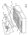
- Figure 9 illustrates a schematic, partially broken away view of a fault tolerant display system 210 capable of supporting mechanisms for optically compensating for failed, defective, or intermittently operating pixels in a display.
- Figure 9 illustrates a mirror based reflective display 240 having row and column physical arrays 242 of pivotal mirrors 244 fixedly mounted to rotate with respect to a substrate 212.
- various other reflective or transmissive display devices including those discussed in connection with Figure 1, can be used in the present invention.
- a virtual gray scale pixel array image 280 on a screen 282 can be produced by controlling the bistable position of each pivotal mirror 244 in the physical array 242, with each mirror selectively controlled to reflect incident light to an absorber (not shown) or allow its transmission to screen 282 via a pixel image displacement mirror 270 (pivotably mounted on an actuator 272) either directly or in conjunction with intervening projective optics, magnifiers, or fixed reflectors (not shown).
- an incident light beam 256 from light source 250 strikes the physical array 242 of light modulators, and is reflected in a desired image pattern toward mirror 270.
- the mirror 270 can be rotated (for example, at a 10Hz, 100HZ, 1000Hz, or greater frequency) by an actuator 272 to displace the beam by a distance corresponding to one or more virtual pixels of the virtual gray scale pixel array image 280.
- Operation of actuator 272 for pivoting the mirror in direction 274 can be enabled in either one, two, or three dimensions by electrostatic attraction, electromagnetic attraction, a piezovibrator, a movable linear stage, an angular arm, or any other conventional mechanism for periodically effecting rotation or movement of mirror 270.
- on-board control electronics 290 can be used for implementing various image processing module units previously described in connection with Figure 8, including mirror fault identification, image rescaling, optional hyperacuity processing and control of mirror 270 for virtual pixel movement.
- Movement of mirror 270 is generally through a distance corresponding to integral multiples of each row or column distance in the virtual gray scale pixel array image 280.
- the mirror 270 can rotate a certain distance sufficient to allow each row 284 in the array 280 to occupy for a brief time the position of an adjacent row 286.
- full two dimensional movement pixel displacement is also possible.
- Figure 10 illustrates yet another embodiment of the present invention for fault tolerant correction of damaged physical pixel arrays.
- Fault tolerant display system 310 supports redundant arrays 385 mounted on substrate 312 for mechanically or optically compensating for failed, defective, or intermittently operating pixels in a display.
- System 310 includes a mirror based reflective display 340 having a row and column physical array 342 of pivotal mirrors 344 mounted for bistable rotation with respect to a substrate 312.
- the reflective display 340 is further mounted on a movable element 314, similar to that discussed in connection with Figure 1, for supporting oscillatory movement of array 342.
- various other reflective or transmissive display devices including those discussed in connection with Figure 1, can be used in the present invention.
- multiple redundant rows or columns are contemplated for operation of alternative embodiments of the present invention, with complete duplication of all rows or columns of physical array 342 being within the scope of the invention.
- a virtual gray scale pixel array image 380 on a screen 382 can be produced by controlling the bistable position of each pivotal mirror 344 in the physical array 342 of light modulators, with each mirror selectively controlled to reflect incident light to an absorber (not shown) or allow its transmission to screen 382 to provide a virtual pixel array image 380.
- incident light beam 356 from light source 350 striking the redundant array 385 of light modulators is ordinarily reflected away from the screen 382.
- the physical array 342 can be oscillated (by piezovibrator 314 in directions 316 and 318, for example) and subjected to various image processing techniques such as discussed in connection with Figure 8 to provide adequate fault correction.
- the foregoing described techniques may be unable to fully compensate for the faults.
- a mirror 370 can be rotated in direction 374 by actuator 372 to map the reflected beam from the redundant array 385 from its initial virtual position (rows 384) onto the position of failed virtual rows 386.
- operation of actuator 372 for pivoting the mirror can be enabled in either one, two, or three dimensions by electrostatic attraction, electromagnetic attraction, a piezovibrator, a movable linear stage, an angular arm, or any other conventional mechanism for periodically effecting rotation or movement of mirror 370.
- the mirror 370 can be fixed in position to direct a virtual pixel image from redundant rows to overlap rows of failed pixels.
- large numbers of redundant rows including as many redundant rows as are present in the physical array 342, can be positioned beside the physical array.
- two highly defective physical arrays can be positioned to project an overlapping virtual array, with the second physical array turning on (when required) only those pixels that are positioned to replace failed pixels in the first physical array.
- Such an embodiment of the present invention allows two costly, yet defective, physical arrays to cooperate to emulate a non-defective array. Since failure rates currently approach 80% to 90% for many varieties of high pixel density physical arrays, the present invention of combining two defective physical arrays can be cost effective.
- overlapping virtual projections from redundant rows and the physical array can be employed in conjunction with an oscillatory fault compensation mechanism such as describe in connection with Figures 1-8.
- the mirror 370 can be rotated in one or two dimensions to track oscillatory movement of the physical array, in a manner similar to that described in connection with Figure 9. This allows large scale row defects to be completely compensated for by virtual projections of redundant arrays, while isolated pixel failures can be corrected for using oscillatory movement and image processing such as discussed in connection with Figures 1-8.
- oscillatory movement allows for straightforward replacement of failed pixels on an array edge.
- the physical array can be surrounded by ten or twenty rows (or columns) of redundant arrays that are transiently moved into position to provide replacement virtual pixels.
Description
- The present invention relates to two dimensional image display systems. More particularly, the present invention relates to fault correction for non-working or damaged pixels of light modulator arrays using separately mounted redundant light modulator arrays.
- High resolution display systems based on discrete two dimensional arrays of reflective or transmissive elements (visually recognized as "pixels") are used in portable computers, LCD multimedia projectors, high definition televisions, flat panel displays, and virtual reality eyewear. As compared to conventional scanning or projection devices (e.g. cathode ray tubes or video projectors), such devices operate at low voltages, making them power efficient, and generally do not require long optical paths for operation, making them space efficient.
- However, widespread adoption of such devices for consumer display systems has been hindered by low manufacturing yields. A typical two dimensional array (using, for example, LCD's that control light transmission or micro-mirrors that control light reflection) may have a million or more discrete elements, with failure of only two or three elements making the display system useless. Even worse, initially operable two dimensional arrays may degrade in performance due to pinpoint screen damage, electronic failures, or mechanical wear and stiction problems. Particularly worrisome are display driver or mounting defects that can cause entire rows or columns of elements in the two dimensional array to simultaneously fail.
- What is needed is an apparatus and technique for providing fault tolerance in two dimensional light modulator arrays of reflective or transmissive elements used in display systems. Fault tolerance should allow for failure of single display elements, multiple display elements, or even failure of multiple rows or columns of display elements without appreciably diminishing display quality. Preferably, fault correction in such a fault tolerant system can be accomplished dynamically, and failure of array elements may even be corrected in real time.
- According to the present invention there is provided a display system comprising
- a light source,
- a display surface,
- a two dimensional light modulator array in an optical path between the light source and the display surface, the two dimensional light modulator array having a plurality of light modulators arranged in rows to modulate light from the source, with at least one row being susceptible to failure,
- a redundant light modulator array having a second plurality of light modulators arranged in at least one row to modulate light from the light source, and
- an optical element positioned to selectively direct light incident on the redundant light modulator array toward the display surface to substitute for at least one failed row of light modulators in the two dimensional light modulator array.
-
- Fault correction employs redundant rows or arrays that are optically moved into position to fully or partially replace defective rows in a two dimensional light modulator array. For example, a display system having a light source and a display surface (which can include a reflective screen, transmissive screen, or even a human eye by use of direct retinal scanning) is used to display an image produced by a two dimensional light modulator array in an optical path between the light source and the display surface. The two dimensional light modulator array has a plurality of light modulators arranged in rows to modulate light from the light source, with at least one row having light modulators susceptible to failure. A redundant light modulator array having a second plurality of light modulators arranged in at least one row can be used to modulate light from the light source, with its light ordinarily being reflected away from the display surface, absorbed, or otherwise made non-perceptible (for example, by shuttering to prevent light hitting the redundant light modulator array). However, if one or more light modulators fail, an optical element (such as a mirror, shutter, etc.), is operated to selectively direct light incident on the redundant light modulator array toward the display surface to substitute for at least one failed light modulator in the row of light modulators in the two dimensional light modulator array. Such a system advantageously allows for effectively replacing one light modulator, one or more rows of the two dimensional light modulator, or even large portions of the two dimensional light modulator with appropriately sized redundant light modulators. As will be appreciated, redundant multiple rows edging (or surrounding) a two dimensional light modulator array can be moved by a movable element to replace edge positioned light modulators. In certain embodiments, it is contemplated to combine movable elements, redundant light modulator arrays, and optical elements to provide various fault correction modes.
- Because of ease of manufacture, predictable performance, and durability, arrays of microelectromechanical pivoting or deformable mirrors controllably movable in response to applied electrostatic or electromagnetic forces are preferred for reflective displays. Such mirror systems are commercially available from Texas Instruments as part of a Digital Mirror Device (DMD) color projection system. Alternatively, switchable diffractive light valves such as developed by Silicon Light Machines, Sunnyvale, CA may be used. In addition, displays based on ferroelectric, electroluminescent, or twisted nematic liquid crystals can also be used. Also suitable are displays that can directly switch to an appropriate transmissive gray level without requiring use of time resolved gray levels such as needed for bistable reflective devices. Generally any device capable of modifying gray levels with a frequency exceeding about 10HZ, or more typically, with a frequency between about 100HZ and 1000Hz, whether directly in response to variable analog current such as with liquid crystals, or through time based techniques such as employed by digital micromirrors or diffractive light valves, can be used in the present invention.
- Figure 1 is a schematic representation of an exemplary two dimensional light modulator array attached to a fixed substrate by an intermediary movable element to allow for controlled physical displacement of the light modulators in row or column directions, with the light modulators being electrostatically actuated bistable mirrors or liquid crystal light absorbers/transmitters that modulate light projected from a light source;
- Figure 2 schematically illustrates a gray scale light modulator array (physical array) for modulating a variable intensity light source, with the light modulator displaying a virtual pixel array, with a single defective light modulator resulting in a dark display pixel;
- Figure 3 schematically illustrates the light modulator array of Figure 2 physically displaced by a single column to effectively share light between the dark display pixel and adjacent pixels;
- Figure 4 schematically illustrates the light modulator array of Figure 3 after image rescaling to adjust image intensity of remaining pixels to match the shared greyscale intensity of the dark display pixel and the adjacent pixel;
- Figure 5 schematically illustrates the light modulator array of Figure 4 after light intensity rescaling to provide a desired greyscale intensity approximating the gray scale background of Figure 2;
- Figure 6 illustrates a light modulator array physically displaced by multiple columns to effectively share light between the dark display pixel and several adjacent pixels;
- Figure 7 is a light modulator array physically displaced by in two dimensions (such as the illustrated rectangular movement) to effectively share light between the dark display pixel and several row and column adjacent pixels;
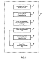
- Figure 8 is a flowchart schematically illustrating modules used for implementing a light modulator failure compensation system;
- Figure 9 illustrates an optical oscillatory pixel displacement system; and Figure 10 illustrates an alternative fault tolerant light modulator array projection system having multiple redundant rows or columns to substitute for non-functioning light modulator rows or columns.
-
- Figure 1 is a schematic, partially broken away view of a fault
tolerant display system 10 capable of supporting mechanisms for mechanically or optically compensating for failed, defective, or intermittently operating pixels in a display. For teaching purposes, Figure 1 illustrates both atransmissive display system 20 and areflective display 40 supported by amovable element 14 on a common fixedsubstrate 12. As shown, thetransmissive display system 20 includes a row andcolumn array 24 of lighttransmissive display elements 28 to selectively transmit or absorb light from alight source 22, while thereflective display system 40 includes a row andcolumn array 42 ofpivotal mirrors 44 that selectively alter reflective direction of light fromlight source 50. However, as will be appreciated, a given display will usually contain either transmissive elements (such as a conventional active matrix LCD projector, LCD display, or ferroelectric fluid display) or reflective elements (such as a digital micromirror disclosed, for example, in U.S. Patent 5,535,047 to Hornbeck), although certain embodiments may combine transmissive and reflective elements for operation (e.g. a stacked transmissive/reflective display using LCD's and a selectively deformable sheet mirror as discussed later in connection with Figure 10). - In operation, each
display element 28 in the lighttransmissive display system 20 can be selectively controlled to absorb incident light or allow its transmission to an image sensor such as a viewer's eye (either directly or in conjunction with intervening projective optics, magnifiers, or reflectors, not shown). In Figure 1, absorption of anincident light ray 32 by an absorbingdisplay element 26 is shown, as is transmission of anincident light ray 30 through atransmissive display element 28. Each display element in the display system is designed to switch between gray scale states in response to control signals sent by control electronics 90 (which can be patterned on the substrate through conventional electronic photolithographic techniques as illustrated, or as a separate control module interfaced with the display through appropriate control leads). As will be appreciated, various conventional light absorbers, ferroelectric fluid displays, LCD displays, or other known light display elements supporting at least two or more light transmissivity states (eg. 256 gray scale) can be used in the present invention. - Gray scale images can also be produced by controlling the bistable position of each
pivotal mirror 44 in the light reflective display system, with each mirror selectively controlled to reflect incident light to an absorber (not shown) or allow its transmission to a viewer's eye (again, either directly or in conjunction with intervening projective optics, magnifiers, or reflectors, not shown). In Figure 1,ray 58 illustrates reflection of anincident light ray 56 fromlight source 50 toward an absorber (not shown) using amirror 48 pivoted through some angle. Reflection of anincident light ray 52 fromlight source 50 toward a viewer (or projective optics, not shown) is illustrated bylight ray 54 reflected from an oppositelytilted mirror 46. A suitable position bistable mirror (operated with electrostatic actuators) for the present invention is described in U.S. Patent 5,535,047 to Hornbeck. As will be appreciated, alternative reflective display systems can be employed, including deformable mirrors, mirrors operated with electromagnetic actuators, or any other conventional reflective system known to those skilled in the art. As withdisplay 20, switching between light absorbing and light reflecting can again be controlled usingcontrol electronics 90. - Switching speed for display elements of any of the foregoing devices will generally be in the millisecond, microsecond, or even nanosecond range, depending on the particular display architecture. Advantageously, use of high speed switching techniques in conjunction with inherent temporal smoothing of a viewer's eye (or other light integrative image sensor) allows for generation of gray levels using high speed switched bistable devices (stable reflective/transmissive or non-reflective/absorptive), with the portion of time that each display element is switched to reflect or transmit light being proportional to the perceived gray level. For example, if the critical light flicker fusion frequency for a viewer is about 60 Hz, a display element switchable at 6 KHz could switch about a 100 times between a light reflective and a non-reflective state without appearing to flicker. By adjusting the proportion of time in each reflective/nonreflective display state, the bistable display element can be used to generate a gray level display. By use of colored light sources and such high speed switching it is even possible to use generate full color displays such as disclosed, for example, in U.S. Patent 5,592,188 to Doherty et al., assigned to Texas Instruments, Inc. Alternatively, systems of colored filters can be used to provide color, as well as gray level displays.
- Unfortunately, in practice it is difficult to manufacture large arrays having hundreds of thousands, or even millions, of the foregoing high switching speed display elements without at least some individual display elements being uncontrollable through mechanical or electrical failure. To compensate for such failures, the array includes a mechanism to physically displace rows or columns in the display array in response to signals sent by
control electronics 90. As illustrated in Figure 1, this mechanism can include themovable element 14, a piezovibrator capable of independently moving in two orthogonal directions as shown byarrows array 24 orarray 42. For example, themovable element 14 can physically move a certain distance sufficient to allow each row in thearray 42 to occupy for a brief time the position of an adjacent row. Alternatively, in addition to adjacent rows, themovable element 14 can be operated to periodically displace each row in the array 24 (or array 42) by two, three, or more rows with respect to its initial starting position with respect to the fixedsubstrate 12. As an extension to one dimensional movement, and as illustrated with respect to Figure 1, the movable element can displace an array 24 (or array 42) in a column direction, as well as in a row direction, to give full two dimensional movement. - Compensation for failure of individual or multiple display elements in such a fault
tolerant display 10 is best described in conjunction with Figures 2, 3, 4, and 5, which shows compensation for a single faileddisplay element 124 in a schematically illustrateddisplay 110. As will be appreciated, although the following description of operation is based on a portion of a single row, pixel displacement can be arbitrary, with row displacement, column displacement, angular displacement, displacement in pixel blocks (using, for example, combinations of row and column displacement) being used. All functioning display elements are shown in a light transmissive (or light reflective) state, with the faileddisplay element 124 being in a light absorptive (or light non-reflective) state. In addition, it will be appreciated that the array is not limited to substantially square or rectangular display pixels, with circular, elliptical, hexagonal, or other suitable geometries. Because of wide availability however, typically an array of rectangular display elements arranged in a rectangular grid are used (eg. 1024 rows by 768 columns of rectangular display elements). - For ease of illustration, in Figure 2 only a portion of a single row of
display 110 in the vicinity of the faileddisplay element 124 is shown. Thedisplay 110 can be transmissive, reflective, emissive, a combination of transmissive and reflective, or any other display architecture able to provide high speed gray scale adjustment to individual pixels. Thedisplay 110 will typically include a two dimensional array of display elements for transmissive or reflective display of an image. Figures 2 through 5 show a variablelight intensity source 114 and a one dimensional partial section of a two dimensionalphysical pixel array 120 consisting of an array of display elements 121-127 (including failed display element 124). As will be appreciated, even though the following discussion is made in terms of gray levels, by use of fixed or movable colored filters, colored emissive displays, or other suitable color producing mechanism, correction of faulty colored display elements is within the scope of the present invention. - Display elements 121-126 are each controlled to display a white pixel in the absence of unintended display element failures, while
display element 127 is controlled to provide a gray pixel (e.g. by time modulation of bistable reflective or transmissive elements, or direct gray scale presentation with LCD's). The display elements 121-127 collectively provide avirtual pixel array 130 consisting of the pixel image of display elements 131-137 developed by application of the variable intensitylight source 114 to thephysical pixel array 120. The intensity of the light source is indicated within the variable light intensity source 114 (intensity 100 in Figure 2, in arbitrary units), the percentage transmissivity/reflectivity of each display element 121-127 is respectively indicated (eg. 0%, 50%, 100%), and the perceived gray level of thevirtual pixel array 130 shown (on a scale of 0 to 100, with 100 being the brightest and 0 being black). In effect, thevirtual pixel array 130 is what a viewer would see when looking at the display, even if thephysical pixel array 120 is undergoing high speed movement in conjunction with image processing driven pixel intensity remapping as discussed in conjunction with Figures 3-5. - As can be seen by inspection of Figure 2,
display element 124 of thephysical pixel array 120 has failed, so that thevirtual pixel array 130 has a correspondingdark pixel element 134. However, if the failure ofdisplay element 124 can be determined, remedial measures to mitigate or entirely correct the failure can be employed. As seen in Figure 3, the light modulator array of Figure 2 can be physically displaced by a single column to effectively share light (through time averaging) between thedark display pixel 134 of thevirtual pixel array 130 and anadjacent pixel 135. The physical displacement is both high speed and oscillatory, with the physical pixels being displaced one column and returned to their original position several tens, hundreds, thousands, or even tens of thousands times each second. It is envisaged that, oscillations on the order of 30 to 100 Hz are generally suitable. Absent any image processing, thevirtual pixel array 130 now does not have a singledark pixel 134, but instead blurs the array to have twogray pixels pixel 127 as seen in Figure 2) derives half of its share of light with the adjacentphysical pixel element 126, brightening the virtualdisplay pixel element 137 from a gray level of 20 to a gray level of 60 (20% + 100% divided by 2 to equal 60% light transmission/reflection/transmission). - Providing a deblurred, rescaled image with the proper relative gray scale for a virtual pixel display elements is schematically illustrated in Figure 4. As seen in Figure 4, image grayscale of
pixels virtual pixel element 133,pixel 123 is scaled to have a grayscale intensity of 50 while physically in a position that providesvirtual pixel 133, and a gray scale intensity of 100 when moved one column leftward into the position that generatesvirtual pixel 134. Similarly,pixel 125 is scaled to have a grayscale intensity of 100 while physically in a position that providesvirtual pixel 135, and a gray scale intensity of 50 when moved one column leftward into the position that generatesvirtual pixel 136. As a result, thevirtual pixel array 130 now displays a uniform grayscale intensity of 50 for each pixel element 131-136. In addition, to provide a correct gray scale forvirtual pixel 137,pixel 126 must be scaled to have a grayscale intensity of 50 while physically in a position that providesvirtual pixel 136, and a gray scale intensity of 10 when moved one column leftward into the position that generatesvirtual pixel 137. As seen in Figure 5, this rescaled image (with elements 131-136 having a perceived grayscale of 50, andelement 137 having a perceived gray scale of 10) is corrected for brightness by doubling (100 to 200) the light intensity of thelight intensity source 114. This brings the perceived gray level back to the target value of 100 for pixels 131-136 (and 20 for pixel 137) in thevirtual pixel array 130. - As will be appreciated, oscillatory movement of a
physical pixel array 120 is not limited to single pixel displacements. Figure 6, which substantially corresponds to the array illustrated in Figure 3, shows displacement of thephysical pixel array 120 by three pixel elements. In contrast to the array illustrated in Figures 2-5, the target value of all pixel elements in Figure 6 is 100, with the single failed pixel having a gray level of 0. The shown displacement allows light from a single failed modulator to be spread among three pixels, decreasing the required intensification of thelight intensity source 114 to bring the perceived level back to its target gray level value of 100. Oscillatory pixel displacement can correspond to five, ten, or more columns (or rows) using suitable actuators and pixel arrays having a suitably high switching speed. - It will be understood that, oscillatory movement can be two dimensional. Figure 7, which substantially corresponds to the array illustrated in Figure 3, shows displacement of the
physical pixel array 120 in two dimensions. Movement is by sequential and repeated column displacement of one pixel leftward, one row upward, one column rightward, and one row downward back to the original position. Again, the target value of all pixel elements is 100, with the single failed pixel having a gray level of 0. This two dimensional displacement allows light from a single failed modulator to be spread among four adjacent pixels, decreasing the required intensification of thelight intensity source 114 to bring the perceived level back to its target gray level value of 100. Oscillatory pixel displacement can be varied to have other oscillatory patterns. For example, movement could be by sequential and repeated column displacement often pixels leftward, one row upward, ten columns rightward, and one row downward back to the original position, to provide a high aspect rectangular pixel displacement orbit (as compared to the square orbit of Figure 7). Other repeating patterns can of course be employed as desired. - The foregoing image processing and display mechanisms are schematically illustrated with reference to Figure 8. In operation, a light modulator
failure compensation system 80 requires a light modulatorfailure identification unit 81 to identify malfunctioning light modulators (physical pixels in a one or two dimensional physical pixel array). Failure identification can be a one-time electronic or optical inspection at a manufacturing facility, or more preferably can be made "on the fly" during device warm-up or operation. Optical identification can be as simple as inspecting an array to see which element is anomalously bright (or dark). Electronic identification can rely on addressing each light modulator to switch optical states (gray levels) while simultaneously measuring capacitance, resistance, or any other suitable electrical switching response properties, with failures being identified by inappropriate electrical responses. For example, an electrostatically actuated micromirror held in a non-reflective state by stiction, damaged supports, or blocking debris would not report a normally expected capacitance change during switching, allowing it to be identified as a failed light modulator. - If any light modulators have failed, the oscillatory pixel displacement unit 82 is utilized to distribute light from two or more physical pixels to each respective virtual pixel in a virtual pixel array seen by a viewer. The physical pixel array is moved by mechanical (as seen in Figures 4-7), optical (as seen in the following Figure 9), or opto-mechanical techniques (as seen in the following Figure 10) that cause periodic displacement of the physical array of light. The extent, directionality, speed, and path of physical pixel array movement can be controlled by on-board or external digital or analog controllers, and can be optionally adjusted to provide for better image compensation. For example, a one dimensional movement of the physical pixel array with a two or three pixel movement shift may be initially adequate for light distribution. However, as additional light modulators fail, two dimensional movement at a higher speed may be required to provide adequate image quality.
- Positional and velocity information from the light modulator
failure identification unit 81 and the oscillatory pixel displacement unit 82 is passed to image processing software or firmware in theimage shift compensator 83. Again, the software can be onboard (directly formed on the substrate as seen in Figure 1), or can be a separate memory and logic module (digital or analog) connected to the oscillatory pixel displacement unit and the electronics necessary for driving pixel image display. Thecompensator 83 is used to shift image position in coordination with periodic displacement of the oscillatory pixel displacement unit 82. In operation, the digital information used to provide a pixel image is periodically shifted one or more pixels in coordination with the movement of the physical array, so that two or more physical pixels together create a virtual pixel. For example, as each pixel was physically moved leftward two pixels, the pixel image display was moved rightward by two pixels, causing each virtual pixel to appear to remain unchanged (and unblurred), even though three physical pixels are actually providing light to a single virtual pixel. - As will be appreciated by those skilled in the art, the
image shift compensator 83 can optionally provide for subpixel display precision using various hyperacuity techniques. For example, sub-pixel edge placement is enabled if specific light modulators are turned on not only while at integral pixel distance intervals, but for some amount of time while at a fractional distance from each integral pixel position. While generally requiring a higher frequency of oscillation of the physical array, hyperacuity techniques based on timing can arbitrarily increase effective display resolution, and are particularly useful for minimizing aliasing features that are easily detected by human viewers. - Information from
units intensity rescaling unit 84. As previously described in connection with Figures 2-5, therescaling unit 84 modifies some or all of the displayed gray levels of light modulators in the physical pixel array. The imageintensity rescaling unit 84 controls this gray level adjustment, with those light modulators positioned adjacent to a failed light modulator generally having the greatest differential gray level adjustment, and/or requiring rapid switching of gray levels (depending on their physical pixel position relative to the virtual pixel). - The loss in overall brightness can optionally be corrected by use of a variable light source intensification unit 85 (corresponding to light
source 50 of Figure 1). Compensation for loss of image brightness is possible by simply increasing brightness of the lightsource intensification unit 85. Such brightness correction is easier if a large number of physical pixels provide each virtual pixel, with a 2:1 physical to virtual pixel ratio (such as discussed in connection with Figures 2-5) requiring a doubling of light source brightness, while a 10:1 ratio only requires about a 10% increase in brightness to provide a fully correctedimage 86. As will be appreciated by those skilled in the art, because of greater viewer acceptance of generalized or localized brightness variations as compared to point or line defects, use of a variable lightsource intensification unit 85 may not be required to satisfy viewer expectations. In such a case, an approximately correctedimage 86 will be displayed, with brightness losses in the vicinity of failed pixel elements being imperceptible or at least not bothersome to a viewer. The present invention contemplates selective image display intensity adjustments in the region of the failed pixels, with minimal or negligible corrections to far removed regions (for example, those regions positioned ten to a hundred pixels away from the failed pixel). Again, because of known limits to human visual perception, such limited compensation may provide adequate fault correction for viewers. - As will be appreciated, movement of the two dimensional light modulator array (whether mechanical or optical or opto-mechanical) does not have to be exclusively through stepwise translation. Instead, movement may occur continuously over a distance of multiple pixels, with acceleration and deceleration occurring when a change of direction of motion is required. Such a continuous motion profile would result in the physical pixels occupying specific virtual pixel locations for different amounts of time. With appropriate modifications, the image
shift compensator unit 83 can utilize information about the position and velocity of the effective array motion to determine the appropriate image shift and intensity corrections such as described in connection with Figure 8. For example, an implementation which utilizes oscillatory translation over a distance of 20 pixels may have uniform velocity in the center of the oscillation, but will move slower at the endpoints. The image shift compensator can obtain information about the motion through position feedback, through velocity feedback, or through other means of prescribing motion, such as a constraining motion to be a function of time, and make corrections as necessary to display a deblurred image. - The present invention provides an alternative to physically moving the array; as discussed in connection with Figure 1, to create a correspondence of two or more physical pixels to each virtual pixel. Figure 9 illustrates a schematic, partially broken away view of a fault
tolerant display system 210 capable of supporting mechanisms for optically compensating for failed, defective, or intermittently operating pixels in a display. For teaching purposes, Figure 9 illustrates a mirror basedreflective display 240 having row and columnphysical arrays 242 ofpivotal mirrors 244 fixedly mounted to rotate with respect to asubstrate 212. However, as those skilled in the art will appreciate, various other reflective or transmissive display devices, including those discussed in connection with Figure 1, can be used in the present invention. - In operation, a virtual gray scale
pixel array image 280 on ascreen 282 can be produced by controlling the bistable position of eachpivotal mirror 244 in thephysical array 242, with each mirror selectively controlled to reflect incident light to an absorber (not shown) or allow its transmission to screen 282 via a pixel image displacement mirror 270 (pivotably mounted on an actuator 272) either directly or in conjunction with intervening projective optics, magnifiers, or fixed reflectors (not shown). As shown in Figure 9, an incident light beam 256 fromlight source 250 strikes thephysical array 242 of light modulators, and is reflected in a desired image pattern towardmirror 270. Themirror 270 can be rotated (for example, at a 10Hz, 100HZ, 1000Hz, or greater frequency) by anactuator 272 to displace the beam by a distance corresponding to one or more virtual pixels of the virtual gray scalepixel array image 280. Operation ofactuator 272 for pivoting the mirror indirection 274 can be enabled in either one, two, or three dimensions by electrostatic attraction, electromagnetic attraction, a piezovibrator, a movable linear stage, an angular arm, or any other conventional mechanism for periodically effecting rotation or movement ofmirror 270. - In a manner similar to that previously discussed in connection with Figure 1, on-
board control electronics 290 can be used for implementing various image processing module units previously described in connection with Figure 8, including mirror fault identification, image rescaling, optional hyperacuity processing and control ofmirror 270 for virtual pixel movement. Movement ofmirror 270 is generally through a distance corresponding to integral multiples of each row or column distance in the virtual gray scalepixel array image 280. For example, in the illustrated embodiment, themirror 270 can rotate a certain distance sufficient to allow eachrow 284 in thearray 280 to occupy for a brief time the position of anadjacent row 286. As will be appreciated, by use of a two dimensional movement ofmirror 270, full two dimensional movement pixel displacement is also possible. - Figure 10 illustrates yet another embodiment of the present invention for fault tolerant correction of damaged physical pixel arrays. Fault
tolerant display system 310 supportsredundant arrays 385 mounted onsubstrate 312 for mechanically or optically compensating for failed, defective, or intermittently operating pixels in a display.System 310 includes a mirror basedreflective display 340 having a row and columnphysical array 342 ofpivotal mirrors 344 mounted for bistable rotation with respect to asubstrate 312. Thereflective display 340 is further mounted on amovable element 314, similar to that discussed in connection with Figure 1, for supporting oscillatory movement ofarray 342. As those skilled in the art will appreciate, various other reflective or transmissive display devices, including those discussed in connection with Figure 1, can be used in the present invention. In addition, multiple redundant rows or columns are contemplated for operation of alternative embodiments of the present invention, with complete duplication of all rows or columns ofphysical array 342 being within the scope of the invention. - In operation, a virtual gray scale
pixel array image 380 on ascreen 382 can be produced by controlling the bistable position of eachpivotal mirror 344 in thephysical array 342 of light modulators, with each mirror selectively controlled to reflect incident light to an absorber (not shown) or allow its transmission to screen 382 to provide a virtualpixel array image 380. In the absence of any pixel defects, incident light beam 356 fromlight source 350 striking theredundant array 385 of light modulators is ordinarily reflected away from thescreen 382. If there are a few point light modulator defects, thephysical array 342 can be oscillated (bypiezovibrator 314 indirections physical array 342 resulting in non-operative virtual pixels (for example, those failed virtual rows 386), the foregoing described techniques may be unable to fully compensate for the faults. - Fortunately, the embodiment of the invention described in relation to Figure 10 allows for large scale compensation of numerous row or column faults. A
mirror 370 can be rotated indirection 374 byactuator 372 to map the reflected beam from theredundant array 385 from its initial virtual position (rows 384) onto the position of failedvirtual rows 386. Like the embodiment of the invention discussed with reference to Figure 9, operation ofactuator 372 for pivoting the mirror can be enabled in either one, two, or three dimensions by electrostatic attraction, electromagnetic attraction, a piezovibrator, a movable linear stage, an angular arm, or any other conventional mechanism for periodically effecting rotation or movement ofmirror 370. Themirror 370 can be fixed in position to direct a virtual pixel image from redundant rows to overlap rows of failed pixels. This can be a one time adjustment of mirror position, or more typically the mirror can be dynamically moved after operation of light modulator failure identification unit (such as described in connection with Figure 8) to create an overlap of the redundant virtual pixels and the failed virtual pixels. In certain embodiments of the invention, large numbers of redundant rows, including as many redundant rows as are present in thephysical array 342, can be positioned beside the physical array. In practice, two highly defective physical arrays can be positioned to project an overlapping virtual array, with the second physical array turning on (when required) only those pixels that are positioned to replace failed pixels in the first physical array. Such an embodiment of the present invention allows two costly, yet defective, physical arrays to cooperate to emulate a non-defective array. Since failure rates currently approach 80% to 90% for many varieties of high pixel density physical arrays, the present invention of combining two defective physical arrays can be cost effective. - As seen in Figure 10, overlapping virtual projections from redundant rows and the physical array can be employed in conjunction with an oscillatory fault compensation mechanism such as describe in connection with Figures 1-8. In those situations where the
physical array 342 of light modulators is oscillating indirections 316 or 318 (as a result of operation of piezovibrator 314), themirror 370 can be rotated in one or two dimensions to track oscillatory movement of the physical array, in a manner similar to that described in connection with Figure 9. This allows large scale row defects to be completely compensated for by virtual projections of redundant arrays, while isolated pixel failures can be corrected for using oscillatory movement and image processing such as discussed in connection with Figures 1-8. In addition, as those skilled in the art will appreciate, oscillatory movement allows for straightforward replacement of failed pixels on an array edge. For example, the physical array can be surrounded by ten or twenty rows (or columns) of redundant arrays that are transiently moved into position to provide replacement virtual pixels.
Claims (7)
- A display system comprisinga lightsource (250),a display surface (282),a two dimensional light modulator array (242) in an optical path between the light source (250) and the display surface 282), the two dimensional light modulator array (242) having a plurality of light modulators (244) arranged in rows to modulate light from the light source (250), with at least one row being susceptible to failure,a redundant light modulator array (242) for substituting said at least one row, said redundant light modulator (242) having a second plurality of light modulators (244) arranged in at least one row to modulate light from the light source (250), characterized byan optical element (270) positioned to selectively direct light incident on the redundant light modulator array (242) toward the display surface (282) to substitute for at least one failed row of light modulators in the two dimensional light modulator array (242).
- The display system of claim 1, wherein the plurality of light modulators (244) reflect light.
- The display system of claim 1 or 2, wherein the optical element (270) selectively directs light incident on at least two rows of the redundant light modulator array (242) to substitute for at least two failed rows of light modulators in the two dimensional light modulator array (242).
- The display system of claim 2 or 3, wherein the optical element (270) further comprises an actuator (272) to move the optical element (270) between predetermined positions.
- The display system of claim 4, wherein the two dimensional light modulator array (342) is movable with respect to the optical element (370), and wherein the optical element (370) is movable to track movement of the two dimensional light modulator array (342).
- The display system of claim 5, wherein the actuator (372) moves the optical element (370) at a frequency greater than about 10kHz.
- The display system of any preceding claim, wherein the redundant light modulator array (242) has substantially as many light modulators as the two dimensional light modulator array (242).
Applications Claiming Priority (2)
| Application Number | Priority Date | Filing Date | Title |
|---|---|---|---|
| US08/883,418 US5815303A (en) | 1997-06-26 | 1997-06-26 | Fault tolerant projective display having redundant light modulators |
| US883418 | 1997-06-26 |
Publications (3)
| Publication Number | Publication Date |
|---|---|
| EP0887681A2 EP0887681A2 (en) | 1998-12-30 |
| EP0887681A3 EP0887681A3 (en) | 2000-01-26 |
| EP0887681B1 true EP0887681B1 (en) | 2002-01-30 |
Family
ID=25382540
Family Applications (1)
| Application Number | Title | Priority Date | Filing Date |
|---|---|---|---|
| EP98303406A Expired - Lifetime EP0887681B1 (en) | 1997-06-26 | 1998-04-30 | Fault tolerant projective display having redundant light modulators |
Country Status (4)
| Country | Link |
|---|---|
| US (1) | US5815303A (en) |
| EP (1) | EP0887681B1 (en) |
| JP (1) | JP4002675B2 (en) |
| DE (1) | DE69803633T2 (en) |
Families Citing this family (190)
| Publication number | Priority date | Publication date | Assignee | Title |
|---|---|---|---|---|
| US6985127B1 (en) * | 1994-09-01 | 2006-01-10 | The United States Of America As Represented By The Secretary Of The Navy | Programmable gray-scale liquid crystal display |
| US6969635B2 (en) * | 2000-12-07 | 2005-11-29 | Reflectivity, Inc. | Methods for depositing, releasing and packaging micro-electromechanical devices on wafer substrates |
| DE19830896A1 (en) * | 1998-07-10 | 2000-06-08 | Mivatec Gmbh | Photo plot process for high-energy recording of a computer-stored raster image on a light-sensitive recording medium |
| WO2000069171A1 (en) * | 1999-05-11 | 2000-11-16 | Digital Electronic Cinema, Inc. | A system and method for defect elimination in large array pixel projectors |
| US7167297B2 (en) * | 2000-08-30 | 2007-01-23 | Reflectivity, Inc | Micromirror array |
| US7569849B2 (en) | 2001-02-16 | 2009-08-04 | Ignis Innovation Inc. | Pixel driver circuit and pixel circuit having the pixel driver circuit |
| EP2267520B1 (en) | 2001-02-27 | 2018-07-25 | Dolby Laboratories Licensing Corporation | A method and device for displaying an image |
| US7023606B2 (en) | 2001-08-03 | 2006-04-04 | Reflectivity, Inc | Micromirror array for projection TV |
| US7145520B2 (en) * | 2001-11-07 | 2006-12-05 | Eastman Kodak Company | Display apparatus box using a spatial light modulator |
| US8687271B2 (en) | 2002-03-13 | 2014-04-01 | Dolby Laboratories Licensing Corporation | N-modulation displays and related methods |
| ES2675880T3 (en) | 2002-03-13 | 2018-07-13 | Dolby Laboratories Licensing Corporation | Failure compensation of light emitting element on a monitor |
| EP2386758A1 (en) | 2002-10-09 | 2011-11-16 | Abbott Diabetes Care Inc. | A method of pumping a predetermined dose of a medical fluid |
| US7727181B2 (en) | 2002-10-09 | 2010-06-01 | Abbott Diabetes Care Inc. | Fluid delivery device with autocalibration |
| US7993108B2 (en) | 2002-10-09 | 2011-08-09 | Abbott Diabetes Care Inc. | Variable volume, shape memory actuated insulin dispensing pump |
| CA2419704A1 (en) | 2003-02-24 | 2004-08-24 | Ignis Innovation Inc. | Method of manufacturing a pixel with organic light-emitting diode |
| US7679407B2 (en) | 2003-04-28 | 2010-03-16 | Abbott Diabetes Care Inc. | Method and apparatus for providing peak detection circuitry for data communication systems |
| CA2443206A1 (en) | 2003-09-23 | 2005-03-23 | Ignis Innovation Inc. | Amoled display backplanes - pixel driver circuits, array architecture, and external compensation |
| DE10345370A1 (en) * | 2003-09-26 | 2005-04-28 | Zeiss Carl Jena Gmbh | Projection apparatus for television device, senses positional offsets in individual opto-mechanical elements and corrects accordingly |
| DE10345371A1 (en) * | 2003-09-26 | 2005-04-28 | Zeiss Carl Jena Gmbh | Arrangement for imaging |
| US6999227B2 (en) * | 2003-10-31 | 2006-02-14 | Intel Corporation | Projection system |
| CA2472671A1 (en) | 2004-06-29 | 2005-12-29 | Ignis Innovation Inc. | Voltage-programming scheme for current-driven amoled displays |
| CA2490858A1 (en) | 2004-12-07 | 2006-06-07 | Ignis Innovation Inc. | Driving method for compensated voltage-programming of amoled displays |
| US20140111567A1 (en) | 2005-04-12 | 2014-04-24 | Ignis Innovation Inc. | System and method for compensation of non-uniformities in light emitting device displays |
| US8599191B2 (en) | 2011-05-20 | 2013-12-03 | Ignis Innovation Inc. | System and methods for extraction of threshold and mobility parameters in AMOLED displays |
| US10013907B2 (en) | 2004-12-15 | 2018-07-03 | Ignis Innovation Inc. | Method and system for programming, calibrating and/or compensating, and driving an LED display |
| US9275579B2 (en) | 2004-12-15 | 2016-03-01 | Ignis Innovation Inc. | System and methods for extraction of threshold and mobility parameters in AMOLED displays |
| JP5128287B2 (en) | 2004-12-15 | 2013-01-23 | イグニス・イノベイション・インコーポレーテッド | Method and system for performing real-time calibration for display arrays |
| US9171500B2 (en) | 2011-05-20 | 2015-10-27 | Ignis Innovation Inc. | System and methods for extraction of parasitic parameters in AMOLED displays |
| US9799246B2 (en) | 2011-05-20 | 2017-10-24 | Ignis Innovation Inc. | System and methods for extraction of threshold and mobility parameters in AMOLED displays |
| US9280933B2 (en) | 2004-12-15 | 2016-03-08 | Ignis Innovation Inc. | System and methods for extraction of threshold and mobility parameters in AMOLED displays |
| US8576217B2 (en) | 2011-05-20 | 2013-11-05 | Ignis Innovation Inc. | System and methods for extraction of threshold and mobility parameters in AMOLED displays |
| US10012678B2 (en) | 2004-12-15 | 2018-07-03 | Ignis Innovation Inc. | Method and system for programming, calibrating and/or compensating, and driving an LED display |
| CA2495726A1 (en) | 2005-01-28 | 2006-07-28 | Ignis Innovation Inc. | Locally referenced voltage programmed pixel for amoled displays |
| CA2496642A1 (en) | 2005-02-10 | 2006-08-10 | Ignis Innovation Inc. | Fast settling time driving method for organic light-emitting diode (oled) displays based on current programming |
| EP1863559A4 (en) | 2005-03-21 | 2008-07-30 | Abbott Diabetes Care Inc | Method and system for providing integrated medication infusion and analyte monitoring system |
| US7768408B2 (en) | 2005-05-17 | 2010-08-03 | Abbott Diabetes Care Inc. | Method and system for providing data management in data monitoring system |
| US7620437B2 (en) | 2005-06-03 | 2009-11-17 | Abbott Diabetes Care Inc. | Method and apparatus for providing rechargeable power in data monitoring and management systems |
| US7852298B2 (en) | 2005-06-08 | 2010-12-14 | Ignis Innovation Inc. | Method and system for driving a light emitting device display |
| CA2510855A1 (en) * | 2005-07-06 | 2007-01-06 | Ignis Innovation Inc. | Fast driving method for amoled displays |
| CA2518276A1 (en) | 2005-09-13 | 2007-03-13 | Ignis Innovation Inc. | Compensation technique for luminance degradation in electro-luminance devices |
| US7756561B2 (en) | 2005-09-30 | 2010-07-13 | Abbott Diabetes Care Inc. | Method and apparatus for providing rechargeable power in data monitoring and management systems |
| US7583190B2 (en) | 2005-10-31 | 2009-09-01 | Abbott Diabetes Care Inc. | Method and apparatus for providing data communication in data monitoring and management systems |
| US8947297B2 (en) * | 2006-01-30 | 2015-02-03 | The Invention Science Fund I, Llc | Positional display elements |
| US8344966B2 (en) | 2006-01-31 | 2013-01-01 | Abbott Diabetes Care Inc. | Method and system for providing a fault tolerant display unit in an electronic device |
| TWI450247B (en) * | 2006-02-10 | 2014-08-21 | Ignis Innovation Inc | Method and system for pixel circuit displays |
| WO2007118332A1 (en) | 2006-04-19 | 2007-10-25 | Ignis Innovation Inc. | Stable driving scheme for active matrix displays |
| CA2556961A1 (en) | 2006-08-15 | 2008-02-15 | Ignis Innovation Inc. | Oled compensation technique based on oled capacitance |
| US8579853B2 (en) | 2006-10-31 | 2013-11-12 | Abbott Diabetes Care Inc. | Infusion devices and methods |
| EP2860721B1 (en) * | 2007-02-01 | 2021-09-01 | Dolby Laboratories Licensing Corporation | Calibration of displays having spatially-variable backlight |
| US20090322800A1 (en) | 2008-06-25 | 2009-12-31 | Dolby Laboratories Licensing Corporation | Method and apparatus in various embodiments for hdr implementation in display devices |
| US8560082B2 (en) | 2009-01-30 | 2013-10-15 | Abbott Diabetes Care Inc. | Computerized determination of insulin pump therapy parameters using real time and retrospective data processing |
| US8531755B2 (en) * | 2009-02-16 | 2013-09-10 | Micronic Laser Systems Ab | SLM device and method combining multiple mirrors for high-power delivery |
| WO2010100273A2 (en) * | 2009-03-06 | 2010-09-10 | Micronic Laser Systems Ab | Variable overlap method and device for stitching together lithographic stripes |
| US8467972B2 (en) | 2009-04-28 | 2013-06-18 | Abbott Diabetes Care Inc. | Closed loop blood glucose control algorithm analysis |
| US10319307B2 (en) | 2009-06-16 | 2019-06-11 | Ignis Innovation Inc. | Display system with compensation techniques and/or shared level resources |
| CA2688870A1 (en) | 2009-11-30 | 2011-05-30 | Ignis Innovation Inc. | Methode and techniques for improving display uniformity |
| US9311859B2 (en) | 2009-11-30 | 2016-04-12 | Ignis Innovation Inc. | Resetting cycle for aging compensation in AMOLED displays |
| CA2669367A1 (en) | 2009-06-16 | 2010-12-16 | Ignis Innovation Inc | Compensation technique for color shift in displays |
| US9384698B2 (en) | 2009-11-30 | 2016-07-05 | Ignis Innovation Inc. | System and methods for aging compensation in AMOLED displays |
| EP3173014B1 (en) | 2009-07-23 | 2021-08-18 | Abbott Diabetes Care, Inc. | Real time management of data relating to physiological control of glucose levels |
| US8633873B2 (en) | 2009-11-12 | 2014-01-21 | Ignis Innovation Inc. | Stable fast programming scheme for displays |
| US10996258B2 (en) | 2009-11-30 | 2021-05-04 | Ignis Innovation Inc. | Defect detection and correction of pixel circuits for AMOLED displays |
| CA2686174A1 (en) * | 2009-12-01 | 2011-06-01 | Ignis Innovation Inc | High reslution pixel architecture |
| US8803417B2 (en) | 2009-12-01 | 2014-08-12 | Ignis Innovation Inc. | High resolution pixel architecture |
| CA2687631A1 (en) | 2009-12-06 | 2011-06-06 | Ignis Innovation Inc | Low power driving scheme for display applications |
| CA2692097A1 (en) | 2010-02-04 | 2011-08-04 | Ignis Innovation Inc. | Extracting correlation curves for light emitting device |
| US10176736B2 (en) | 2010-02-04 | 2019-01-08 | Ignis Innovation Inc. | System and methods for extracting correlation curves for an organic light emitting device |
| US20140313111A1 (en) | 2010-02-04 | 2014-10-23 | Ignis Innovation Inc. | System and methods for extracting correlation curves for an organic light emitting device |
| US10163401B2 (en) | 2010-02-04 | 2018-12-25 | Ignis Innovation Inc. | System and methods for extracting correlation curves for an organic light emitting device |
| US9881532B2 (en) | 2010-02-04 | 2018-01-30 | Ignis Innovation Inc. | System and method for extracting correlation curves for an organic light emitting device |
| US10089921B2 (en) | 2010-02-04 | 2018-10-02 | Ignis Innovation Inc. | System and methods for extracting correlation curves for an organic light emitting device |
| EP2542941B1 (en) * | 2010-03-05 | 2015-05-06 | Micronic Mydata AB | 1.5d slm for lithography |
| CA2696778A1 (en) | 2010-03-17 | 2011-09-17 | Ignis Innovation Inc. | Lifetime, uniformity, parameter extraction methods |
| US9161448B2 (en) | 2010-03-29 | 2015-10-13 | Semprius, Inc. | Laser assisted transfer welding process |
| US9142468B2 (en) | 2010-08-26 | 2015-09-22 | Semprius, Inc. | Structures and methods for testing printable integrated circuits |
| US9899329B2 (en) | 2010-11-23 | 2018-02-20 | X-Celeprint Limited | Interconnection structures and methods for transfer-printed integrated circuit elements with improved interconnection alignment tolerance |
| US8907991B2 (en) | 2010-12-02 | 2014-12-09 | Ignis Innovation Inc. | System and methods for thermal compensation in AMOLED displays |
| US9606607B2 (en) | 2011-05-17 | 2017-03-28 | Ignis Innovation Inc. | Systems and methods for display systems with dynamic power control |
| WO2012156942A1 (en) | 2011-05-17 | 2012-11-22 | Ignis Innovation Inc. | Systems and methods for display systems with dynamic power control |
| US9530349B2 (en) | 2011-05-20 | 2016-12-27 | Ignis Innovations Inc. | Charged-based compensation and parameter extraction in AMOLED displays |
| US9466240B2 (en) | 2011-05-26 | 2016-10-11 | Ignis Innovation Inc. | Adaptive feedback system for compensating for aging pixel areas with enhanced estimation speed |
| CN106910464B (en) | 2011-05-27 | 2020-04-24 | 伊格尼斯创新公司 | System for compensating pixels in a display array and pixel circuit for driving light emitting devices |
| US8934259B2 (en) | 2011-06-08 | 2015-01-13 | Semprius, Inc. | Substrates with transferable chiplets |
| US8901579B2 (en) | 2011-08-03 | 2014-12-02 | Ignis Innovation Inc. | Organic light emitting diode and method of manufacturing |
| US9070775B2 (en) | 2011-08-03 | 2015-06-30 | Ignis Innovations Inc. | Thin film transistor |
| US9412727B2 (en) | 2011-09-20 | 2016-08-09 | Semprius, Inc. | Printing transferable components using microstructured elastomeric surfaces with pressure modulated reversible adhesion |
| US9324268B2 (en) | 2013-03-15 | 2016-04-26 | Ignis Innovation Inc. | Amoled displays with multiple readout circuits |
| US9385169B2 (en) | 2011-11-29 | 2016-07-05 | Ignis Innovation Inc. | Multi-functional active matrix organic light-emitting diode display |
| US10089924B2 (en) | 2011-11-29 | 2018-10-02 | Ignis Innovation Inc. | Structural and low-frequency non-uniformity compensation |
| US8937632B2 (en) | 2012-02-03 | 2015-01-20 | Ignis Innovation Inc. | Driving system for active-matrix displays |
| US9190456B2 (en) | 2012-04-25 | 2015-11-17 | Ignis Innovation Inc. | High resolution display panel with emissive organic layers emitting light of different colors |
| US9747834B2 (en) | 2012-05-11 | 2017-08-29 | Ignis Innovation Inc. | Pixel circuits including feedback capacitors and reset capacitors, and display systems therefore |
| US8922544B2 (en) | 2012-05-23 | 2014-12-30 | Ignis Innovation Inc. | Display systems with compensation for line propagation delay |
| US9786223B2 (en) | 2012-12-11 | 2017-10-10 | Ignis Innovation Inc. | Pixel circuits for AMOLED displays |
| US9336717B2 (en) | 2012-12-11 | 2016-05-10 | Ignis Innovation Inc. | Pixel circuits for AMOLED displays |
| US9830857B2 (en) | 2013-01-14 | 2017-11-28 | Ignis Innovation Inc. | Cleaning common unwanted signals from pixel measurements in emissive displays |
| WO2014108879A1 (en) | 2013-01-14 | 2014-07-17 | Ignis Innovation Inc. | Driving scheme for emissive displays providing compensation for driving transistor variations |
| US9721505B2 (en) | 2013-03-08 | 2017-08-01 | Ignis Innovation Inc. | Pixel circuits for AMOLED displays |
| EP3043338A1 (en) | 2013-03-14 | 2016-07-13 | Ignis Innovation Inc. | Re-interpolation with edge detection for extracting an aging pattern for amoled displays |
| DE112014001402T5 (en) | 2013-03-15 | 2016-01-28 | Ignis Innovation Inc. | Dynamic adjustment of touch resolutions of an Amoled display |
| WO2014174427A1 (en) | 2013-04-22 | 2014-10-30 | Ignis Innovation Inc. | Inspection system for oled display panels |
| TW201504727A (en) * | 2013-07-24 | 2015-02-01 | Hon Hai Prec Ind Co Ltd | Backlight module and display device |
| DE112014003719T5 (en) | 2013-08-12 | 2016-05-19 | Ignis Innovation Inc. | compensation accuracy |
| US9741282B2 (en) | 2013-12-06 | 2017-08-22 | Ignis Innovation Inc. | OLED display system and method |
| US9761170B2 (en) | 2013-12-06 | 2017-09-12 | Ignis Innovation Inc. | Correction for localized phenomena in an image array |
| US9502653B2 (en) | 2013-12-25 | 2016-11-22 | Ignis Innovation Inc. | Electrode contacts |
| US10997901B2 (en) | 2014-02-28 | 2021-05-04 | Ignis Innovation Inc. | Display system |
| US10176752B2 (en) | 2014-03-24 | 2019-01-08 | Ignis Innovation Inc. | Integrated gate driver |
| DE102015206281A1 (en) | 2014-04-08 | 2015-10-08 | Ignis Innovation Inc. | Display system with shared level resources for portable devices |
| WO2015193433A2 (en) | 2014-06-18 | 2015-12-23 | X-Celeprint Limited | Micro assembled high frequency devices and arrays |
| CN110010750B (en) | 2014-06-18 | 2021-11-09 | 艾克斯展示公司技术有限公司 | Micro-assembly LED display |
| US9929053B2 (en) | 2014-06-18 | 2018-03-27 | X-Celeprint Limited | Systems and methods for controlling release of transferable semiconductor structures |
| US9865600B2 (en) | 2014-06-18 | 2018-01-09 | X-Celeprint Limited | Printed capacitors |
| EP3157858B1 (en) | 2014-06-18 | 2018-12-26 | X-Celeprint Limited | Systems and methods for controlling release of transferable semiconductor structures |
| EP3158593A1 (en) | 2014-06-18 | 2017-04-26 | X-Celeprint Limited | Systems and methods for preparing gan and related materials for micro assembly |
| US11472171B2 (en) | 2014-07-20 | 2022-10-18 | X Display Company Technology Limited | Apparatus and methods for micro-transfer-printing |
| US9716082B2 (en) | 2014-08-26 | 2017-07-25 | X-Celeprint Limited | Micro assembled hybrid displays and lighting elements |
| US9537069B1 (en) | 2014-09-25 | 2017-01-03 | X-Celeprint Limited | Inorganic light-emitting diode with encapsulating reflector |
| US9468050B1 (en) | 2014-09-25 | 2016-10-11 | X-Celeprint Limited | Self-compensating circuit for faulty display pixels |
| US9799719B2 (en) | 2014-09-25 | 2017-10-24 | X-Celeprint Limited | Active-matrix touchscreen |
| US9818725B2 (en) | 2015-06-01 | 2017-11-14 | X-Celeprint Limited | Inorganic-light-emitter display with integrated black matrix |
| US9991163B2 (en) | 2014-09-25 | 2018-06-05 | X-Celeprint Limited | Small-aperture-ratio display with electrical component |
| US9799261B2 (en) | 2014-09-25 | 2017-10-24 | X-Celeprint Limited | Self-compensating circuit for faulty display pixels |
| CA2872563A1 (en) | 2014-11-28 | 2016-05-28 | Ignis Innovation Inc. | High pixel density array architecture |
| CA2879462A1 (en) | 2015-01-23 | 2016-07-23 | Ignis Innovation Inc. | Compensation for color variation in emissive devices |
| CA2889870A1 (en) | 2015-05-04 | 2016-11-04 | Ignis Innovation Inc. | Optical feedback system |
| US9640715B2 (en) | 2015-05-15 | 2017-05-02 | X-Celeprint Limited | Printable inorganic semiconductor structures |
| CA2892714A1 (en) | 2015-05-27 | 2016-11-27 | Ignis Innovation Inc | Memory bandwidth reduction in compensation system |
| US9871345B2 (en) | 2015-06-09 | 2018-01-16 | X-Celeprint Limited | Crystalline color-conversion device |
| US10102794B2 (en) | 2015-06-09 | 2018-10-16 | X-Celeprint Limited | Distributed charge-pump power-supply system |
| US11061276B2 (en) | 2015-06-18 | 2021-07-13 | X Display Company Technology Limited | Laser array display |
| US10133426B2 (en) | 2015-06-18 | 2018-11-20 | X-Celeprint Limited | Display with micro-LED front light |
| US9704821B2 (en) | 2015-08-11 | 2017-07-11 | X-Celeprint Limited | Stamp with structured posts |
| US10255834B2 (en) | 2015-07-23 | 2019-04-09 | X-Celeprint Limited | Parallel redundant chiplet system for controlling display pixels |
| US10373554B2 (en) | 2015-07-24 | 2019-08-06 | Ignis Innovation Inc. | Pixels and reference circuits and timing techniques |
| CA2898282A1 (en) | 2015-07-24 | 2017-01-24 | Ignis Innovation Inc. | Hybrid calibration of current sources for current biased voltage progra mmed (cbvp) displays |
| US10657895B2 (en) | 2015-07-24 | 2020-05-19 | Ignis Innovation Inc. | Pixels and reference circuits and timing techniques |
| CA2900170A1 (en) | 2015-08-07 | 2017-02-07 | Gholamreza Chaji | Calibration of pixel based on improved reference values |
| US9640108B2 (en) | 2015-08-25 | 2017-05-02 | X-Celeprint Limited | Bit-plane pulse width modulated digital display system |
| US10468363B2 (en) | 2015-08-10 | 2019-11-05 | X-Celeprint Limited | Chiplets with connection posts |
| US10380930B2 (en) | 2015-08-24 | 2019-08-13 | X-Celeprint Limited | Heterogeneous light emitter display system |
| US10230048B2 (en) | 2015-09-29 | 2019-03-12 | X-Celeprint Limited | OLEDs for micro transfer printing |
| CA2909813A1 (en) | 2015-10-26 | 2017-04-26 | Ignis Innovation Inc | High ppi pattern orientation |
| US10066819B2 (en) | 2015-12-09 | 2018-09-04 | X-Celeprint Limited | Micro-light-emitting diode backlight system |
| US10091446B2 (en) | 2015-12-23 | 2018-10-02 | X-Celeprint Limited | Active-matrix displays with common pixel control |
| US9786646B2 (en) | 2015-12-23 | 2017-10-10 | X-Celeprint Limited | Matrix addressed device repair |
| US9930277B2 (en) | 2015-12-23 | 2018-03-27 | X-Celeprint Limited | Serial row-select matrix-addressed system |
| US9928771B2 (en) | 2015-12-24 | 2018-03-27 | X-Celeprint Limited | Distributed pulse width modulation control |
| US10361677B2 (en) | 2016-02-18 | 2019-07-23 | X-Celeprint Limited | Transverse bulk acoustic wave filter |
| US10200013B2 (en) | 2016-02-18 | 2019-02-05 | X-Celeprint Limited | Micro-transfer-printed acoustic wave filter device |
| US10109753B2 (en) | 2016-02-19 | 2018-10-23 | X-Celeprint Limited | Compound micro-transfer-printed optical filter device |
| US10217730B2 (en) | 2016-02-25 | 2019-02-26 | X-Celeprint Limited | Efficiently micro-transfer printing micro-scale devices onto large-format substrates |
| US10193025B2 (en) | 2016-02-29 | 2019-01-29 | X-Celeprint Limited | Inorganic LED pixel structure |
| US10150326B2 (en) | 2016-02-29 | 2018-12-11 | X-Celeprint Limited | Hybrid document with variable state |
| US10150325B2 (en) | 2016-02-29 | 2018-12-11 | X-Celeprint Limited | Hybrid banknote with electronic indicia |
| US10153256B2 (en) | 2016-03-03 | 2018-12-11 | X-Celeprint Limited | Micro-transfer printable electronic component |
| US10153257B2 (en) | 2016-03-03 | 2018-12-11 | X-Celeprint Limited | Micro-printed display |
| US10103069B2 (en) | 2016-04-01 | 2018-10-16 | X-Celeprint Limited | Pressure-activated electrical interconnection by micro-transfer printing |
| US10199546B2 (en) | 2016-04-05 | 2019-02-05 | X-Celeprint Limited | Color-filter device |
| US10008483B2 (en) | 2016-04-05 | 2018-06-26 | X-Celeprint Limited | Micro-transfer printed LED and color filter structure |
| US9997102B2 (en) | 2016-04-19 | 2018-06-12 | X-Celeprint Limited | Wirelessly powered display and system |
| US10198890B2 (en) | 2016-04-19 | 2019-02-05 | X-Celeprint Limited | Hybrid banknote with electronic indicia using near-field-communications |
| US10360846B2 (en) | 2016-05-10 | 2019-07-23 | X-Celeprint Limited | Distributed pulse-width modulation system with multi-bit digital storage and output device |
| US10622700B2 (en) | 2016-05-18 | 2020-04-14 | X-Celeprint Limited | Antenna with micro-transfer-printed circuit element |
| US9997501B2 (en) | 2016-06-01 | 2018-06-12 | X-Celeprint Limited | Micro-transfer-printed light-emitting diode device |
| US10453826B2 (en) | 2016-06-03 | 2019-10-22 | X-Celeprint Limited | Voltage-balanced serial iLED pixel and display |
| US11137641B2 (en) | 2016-06-10 | 2021-10-05 | X Display Company Technology Limited | LED structure with polarized light emission |
| US10222698B2 (en) | 2016-07-28 | 2019-03-05 | X-Celeprint Limited | Chiplets with wicking posts |
| US11064609B2 (en) | 2016-08-04 | 2021-07-13 | X Display Company Technology Limited | Printable 3D electronic structure |
| US9980341B2 (en) | 2016-09-22 | 2018-05-22 | X-Celeprint Limited | Multi-LED components |
| US10157880B2 (en) | 2016-10-03 | 2018-12-18 | X-Celeprint Limited | Micro-transfer printing with volatile adhesive layer |
| US10782002B2 (en) | 2016-10-28 | 2020-09-22 | X Display Company Technology Limited | LED optical components |
| US10347168B2 (en) | 2016-11-10 | 2019-07-09 | X-Celeprint Limited | Spatially dithered high-resolution |
| TWI739949B (en) | 2016-11-15 | 2021-09-21 | 愛爾蘭商艾克斯展示公司技術有限公司 | Micro-transfer-printable flip-chip structures and methods |
| US10600671B2 (en) | 2016-11-15 | 2020-03-24 | X-Celeprint Limited | Micro-transfer-printable flip-chip structures and methods |
| US10395966B2 (en) | 2016-11-15 | 2019-08-27 | X-Celeprint Limited | Micro-transfer-printable flip-chip structures and methods |
| DE102017222059A1 (en) | 2016-12-06 | 2018-06-07 | Ignis Innovation Inc. | Pixel circuits for reducing hysteresis |
| US10297502B2 (en) | 2016-12-19 | 2019-05-21 | X-Celeprint Limited | Isolation structure for micro-transfer-printable devices |
| US10438859B2 (en) | 2016-12-19 | 2019-10-08 | X-Celeprint Limited | Transfer printed device repair |
| CN106527059A (en) * | 2016-12-31 | 2017-03-22 | 俞庆平 | Interested region use method in laser direct writing field |
| US10832609B2 (en) | 2017-01-10 | 2020-11-10 | X Display Company Technology Limited | Digital-drive pulse-width-modulated output system |
| US10396137B2 (en) | 2017-03-10 | 2019-08-27 | X-Celeprint Limited | Testing transfer-print micro-devices on wafer |
| US11024608B2 (en) | 2017-03-28 | 2021-06-01 | X Display Company Technology Limited | Structures and methods for electrical connection of micro-devices and substrates |
| US10714018B2 (en) | 2017-05-17 | 2020-07-14 | Ignis Innovation Inc. | System and method for loading image correction data for displays |
| US11025899B2 (en) | 2017-08-11 | 2021-06-01 | Ignis Innovation Inc. | Optical correction systems and methods for correcting non-uniformity of emissive display devices |
| US10832935B2 (en) | 2017-08-14 | 2020-11-10 | X Display Company Technology Limited | Multi-level micro-device tethers |
| US10971078B2 (en) | 2018-02-12 | 2021-04-06 | Ignis Innovation Inc. | Pixel measurement through data line |
| US10832934B2 (en) | 2018-06-14 | 2020-11-10 | X Display Company Technology Limited | Multi-layer tethers for micro-transfer printing |
| US10714001B2 (en) | 2018-07-11 | 2020-07-14 | X Display Company Technology Limited | Micro-light-emitting-diode displays |
| US10748793B1 (en) | 2019-02-13 | 2020-08-18 | X Display Company Technology Limited | Printing component arrays with different orientations |
Family Cites Families (18)
| Publication number | Priority date | Publication date | Assignee | Title |
|---|---|---|---|---|
| EP0460890A3 (en) * | 1990-06-06 | 1992-11-25 | Texas Instruments Incorporated | Optical tracking system |
| JPH04194814A (en) * | 1990-11-22 | 1992-07-14 | Minolta Camera Co Ltd | Light beam scanning optical system |
| US5132723A (en) * | 1991-09-05 | 1992-07-21 | Creo Products, Inc. | Method and apparatus for exposure control in light valves |
| CA2081753C (en) * | 1991-11-22 | 2002-08-06 | Jeffrey B. Sampsell | Dmd scanner |
| US5231388A (en) * | 1991-12-17 | 1993-07-27 | Texas Instruments Incorporated | Color display system using spatial light modulators |
| JP3547015B2 (en) * | 1993-01-07 | 2004-07-28 | ソニー株式会社 | Image display device and method for improving resolution of image display device |
| JP3318904B2 (en) * | 1993-07-14 | 2002-08-26 | テキサス インスツルメンツ インコーポレイテツド | Projector equipment |
| US5517347A (en) * | 1993-12-01 | 1996-05-14 | Texas Instruments Incorporated | Direct view deformable mirror device |
| US5600459A (en) * | 1993-12-20 | 1997-02-04 | Roy; Howard S. | Multiple-shutter flat-panel display having individually controlled pixels and method for making same |
| US5729245A (en) * | 1994-03-21 | 1998-03-17 | Texas Instruments Incorporated | Alignment for display having multiple spatial light modulators |
| US5673106A (en) * | 1994-06-17 | 1997-09-30 | Texas Instruments Incorporated | Printing system with self-monitoring and adjustment |
| US5504504A (en) * | 1994-07-13 | 1996-04-02 | Texas Instruments Incorporated | Method of reducing the visual impact of defects present in a spatial light modulator display |
| US5630027A (en) * | 1994-12-28 | 1997-05-13 | Texas Instruments Incorporated | Method and apparatus for compensating horizontal and vertical alignment errors in display systems |
| US5592188A (en) * | 1995-01-04 | 1997-01-07 | Texas Instruments Incorporated | Method and system for accentuating intense white display areas in sequential DMD video systems |
| US5612713A (en) * | 1995-01-06 | 1997-03-18 | Texas Instruments Incorporated | Digital micro-mirror device with block data loading |
| JP3549647B2 (en) * | 1995-06-13 | 2004-08-04 | 富士写真フイルム株式会社 | Image exposure method using display panel |
| US5877844A (en) * | 1995-06-13 | 1999-03-02 | Fuji Photo Film Co., Ltd. | Image exposure method using display panel |
| US5699168A (en) * | 1995-06-22 | 1997-12-16 | Texas Instruments Incorporated | Grayscale printing with sliding window memory |
-
1997
- 1997-06-26 US US08/883,418 patent/US5815303A/en not_active Expired - Lifetime
-
1998
- 1998-04-30 EP EP98303406A patent/EP0887681B1/en not_active Expired - Lifetime
- 1998-04-30 DE DE69803633T patent/DE69803633T2/en not_active Expired - Lifetime
- 1998-06-17 JP JP17027898A patent/JP4002675B2/en not_active Expired - Fee Related
Also Published As
| Publication number | Publication date |
|---|---|
| JP4002675B2 (en) | 2007-11-07 |
| EP0887681A2 (en) | 1998-12-30 |
| JPH1124016A (en) | 1999-01-29 |
| DE69803633T2 (en) | 2002-06-13 |
| US5815303A (en) | 1998-09-29 |
| EP0887681A3 (en) | 2000-01-26 |
| DE69803633D1 (en) | 2002-03-14 |
Similar Documents
| Publication | Publication Date | Title |
|---|---|---|
| EP0887681B1 (en) | Fault tolerant projective display having redundant light modulators | |
| EP0887690B1 (en) | Fault tolerant light modulator display system | |
| EP0887689B1 (en) | Optical row displacement for a fault tolerant projective display | |
| KR100346879B1 (en) | Display device and method of reducing the visual impact of defects | |
| TWI778098B (en) | Light emitter architecture for scanning display device | |
| EP0657760A1 (en) | Image simulation and projection system | |
| JP5402791B2 (en) | projector | |
| US7034784B2 (en) | Optical shifter and optical display system | |
| US20060176323A1 (en) | Optical system and method for increasing image resolution and/or dithering in projection applications | |
| JP2008039795A (en) | Multi-display system | |
| JP6492427B2 (en) | Liquid crystal display device, electronic apparatus, and driving method of liquid crystal display device | |
| US20060176362A1 (en) | Optical system and method for increasing image resolution and/or dithering in printing applications | |
| US11297290B2 (en) | Projector and method for controlling projector | |
| US8567956B2 (en) | Projector | |
| US20070177113A1 (en) | Digital image projection methods and apparatus thereof | |
| JP5059446B2 (en) | Display device, projection display device, optical path shift element control circuit, and optical path shift element | |
| JP4346125B2 (en) | Display system | |
| US11095862B2 (en) | Optical module having pixel shifting mechanism transitioning to first state or second state, method for controlling the same, and projection-type display apparatus | |
| US20080055340A1 (en) | Display apparatus including optical modulator and image controlling method | |
| KR20060030606A (en) | Micro-mirror optical modulator and projection display apparatus using of the same | |
| JP2002357809A (en) | Picture display device | |
| CN117666123A (en) | Image source assembly, display device and vehicle | |
| JP2024502701A (en) | Image projector with laser scanning on spatial light modulator | |
| JP2020154197A (en) | Optical module and control method of the same, and projection type display device | |
| JPH08262565A (en) | Picture projection device |
Legal Events
| Date | Code | Title | Description |
|---|---|---|---|
| PUAI | Public reference made under article 153(3) epc to a published international application that has entered the european phase |
Free format text: ORIGINAL CODE: 0009012 |
|
| AK | Designated contracting states |
Kind code of ref document: A2 Designated state(s): DE FR GB |
|
| AX | Request for extension of the european patent |
Free format text: AL;LT;LV;MK;RO;SI |
|
| PUAL | Search report despatched |
Free format text: ORIGINAL CODE: 0009013 |
|
| AK | Designated contracting states |
Kind code of ref document: A3 Designated state(s): AT BE CH CY DE DK ES FI FR GB GR IE IT LI LU MC NL PT SE |
|
| AX | Request for extension of the european patent |
Free format text: AL;LT;LV;MK;RO;SI |
|
| RIC1 | Information provided on ipc code assigned before grant |
Free format text: 7G 02B 26/08 A, 7H 04N 5/74 B |
|
| 17P | Request for examination filed |
Effective date: 20000726 |
|
| AKX | Designation fees paid |
Free format text: DE FR GB |
|
| 17Q | First examination report despatched |
Effective date: 20000919 |
|
| GRAG | Despatch of communication of intention to grant |
Free format text: ORIGINAL CODE: EPIDOS AGRA |
|
| GRAG | Despatch of communication of intention to grant |
Free format text: ORIGINAL CODE: EPIDOS AGRA |
|
| GRAH | Despatch of communication of intention to grant a patent |
Free format text: ORIGINAL CODE: EPIDOS IGRA |
|
| GRAH | Despatch of communication of intention to grant a patent |
Free format text: ORIGINAL CODE: EPIDOS IGRA |
|
| GRAA | (expected) grant |
Free format text: ORIGINAL CODE: 0009210 |
|
| REG | Reference to a national code |
Ref country code: GB Ref legal event code: IF02 |
|
| AK | Designated contracting states |
Kind code of ref document: B1 Designated state(s): DE FR GB |
|
| REF | Corresponds to: |
Ref document number: 69803633 Country of ref document: DE Date of ref document: 20020314 |
|
| ET | Fr: translation filed | ||
| PLBE | No opposition filed within time limit |
Free format text: ORIGINAL CODE: 0009261 |
|
| STAA | Information on the status of an ep patent application or granted ep patent |
Free format text: STATUS: NO OPPOSITION FILED WITHIN TIME LIMIT |
|
| 26N | No opposition filed | ||
| REG | Reference to a national code |
Ref country code: FR Ref legal event code: PLFP Year of fee payment: 19 |
|
| PGFP | Annual fee paid to national office [announced via postgrant information from national office to epo] |
Ref country code: GB Payment date: 20160324 Year of fee payment: 19 Ref country code: FR Payment date: 20160323 Year of fee payment: 19 |
|
| PGFP | Annual fee paid to national office [announced via postgrant information from national office to epo] |
Ref country code: DE Payment date: 20160321 Year of fee payment: 19 |
|
| REG | Reference to a national code |
Ref country code: DE Ref legal event code: R119 Ref document number: 69803633 Country of ref document: DE |
|
| GBPC | Gb: european patent ceased through non-payment of renewal fee |
Effective date: 20170430 |
|
| REG | Reference to a national code |
Ref country code: FR Ref legal event code: ST Effective date: 20171229 |
|
| PG25 | Lapsed in a contracting state [announced via postgrant information from national office to epo] |
Ref country code: DE Free format text: LAPSE BECAUSE OF NON-PAYMENT OF DUE FEES Effective date: 20171103 Ref country code: FR Free format text: LAPSE BECAUSE OF NON-PAYMENT OF DUE FEES Effective date: 20170502 |
|
| PG25 | Lapsed in a contracting state [announced via postgrant information from national office to epo] |
Ref country code: GB Free format text: LAPSE BECAUSE OF NON-PAYMENT OF DUE FEES Effective date: 20170430 |