BACKGROUND OF THE INVENTION
1.Field of the Invention
The present invention relates to an antenna device,
for example, AM broadcasting, FM broadcasting, TV
broadcasting or wireless telephone, etc., which is
particularly attached to a body of an automobile, etc.
2.Related Art of the Invention
With the development of car multimedia times, in the
recent years, not only AM/FM radio but also various radio
units such as TV, a radio telephone or a navigation system
are being mounted also on an automobile, and it is expected
that, in the future, information and service which are
supplied by radio waves are more and more increased
so that the importance of the antenna is more and more
heightened.
In general, in the case of equipping an automobile
or the like with an antenna, a car body formed of a
conductive base plate adversely affects the performance
of the antenna such as a directional gain. Conventionally,
considering that the antenna is installed to a car body,
for example, a monopole, a rod antenna, a V dipole antenna
or the like are employed as the antenna used for the
automobile. Most of those antennas are provided so as to
project a long bar-shaped antenna element from the car
body.
However, as described above, the antenna provided so
as to project from the car body the long bar-shaped antenna
element or the like which is generally used for the
automobile suffers from various problems such that not
only the beauty of the appearance is lost, but also wind
sound occurs, there is a risk that the antenna is robbed,
the antenna must be removed when washing the automobile,
and so on.
SUMMARY OF THE INVENTION
The present invention has been made to eliminate the
above problems with the conventional antennas, and
therefore an object of the present invention is to provide
an antenna device which is capable of being equipped in
the vicinity of a body of an automobile or being integrated
with the body so as to be equipped on a plane and also
capable of being downsized so an to be equipped even in
a small location.
In order to achieve the above object, according to
one aspect of the present invention, an antenna device
includes at least one linear conductor each having at least
one bent or curved portion for a feeder section.
According to another aspect of the present invention,
in the above antenna device, the linear conductor has four
or more even numbers of bent or curved portions.
According to further aspect of the present invention,
the above antenna device includes at least one or more
spiral linear conductor for the feeder section.
The above structure enables the antenna to be disposed
within a slender casing.
According to further aspect of the present invention,
an antenna device is disposed in the vicinity of a
conductive base plate so that an earth terminal of the
antenna is connected to the conductive base plate.
The above structure enables to obtain desired
impedance characteristic and directivity.
According to still another aspect of the present
invention, an antenna device is disposed in the vicinity
of a conductive base plate, and a switching device is
disposed between an earth terminal of the antenna and the
conductive base plate.
The above structure enables to select desired
impedance characteristic and directivity.
According to still another aspect of the present
invention, an antenna device includes an antenna formed
of an antenna element group into which a plurality of
antenna elements are unified by a single feeder section.
The above structure enables to realize an antenna
small in size and high in gain covers a desired frequency
band.
According to still another aspect of the present
invention, an antenna device includes an antenna formed
of an antenna element group in which taps are formed at
predetermined positions of a plurality of antenna
elements, respectively, and those taps are joined
together to form a single feeder section.
The above structure enables to realize an antenna
small in size and high in gain which covers a desired
frequency band by an easy feeding method.
According to still another aspect of the present
invention, in an antenna device, tuning frequency is
controlled by setting the coupling of opposed open
terminal portions of an antenna element.
According to still another aspect of the present
invention, in an antenna device, a tuning frequency is
controlled by setting the coupling of an open terminal
of an antenna element and a neutral point thereof or
opposed portions thereof in the vicinity of the neutral
point.
According to yet another aspect of the present
invention, in an antenna device, at least one linear
conductor is connected to both poles of a coil,
respectively, and an earth terminal is formed at the
neutral point of the coil, and a tap is formed at a
predetermined position of the respective linear
conductors or the coil, from which a feeding terminal is
led out.
According to yet another aspect of the present
invention, in an antenna device, one or more linear
conductors are provided for a feeder section through a
coil.
According to still another aspect of the present
invention, in the above antenna device, at least one
antenna is selected from a plurality of antennas under
control.
According to yet another aspect of the present
invention, in the above antenna device, an antenna maximum
in a receiver input is selected under control in the
control for selecting a plurality of antennas.
According to still another aspect of the present
invention, in the antenna device as defined in the above,
an antenna minimum in multi-pass interference level is
selected under control in the control for selecting a
plurality of antennas.
According to yet another aspect of the present
invention, in the antenna device as defined in the above,
the antenna element is disposed in a recess of the
conductive base plate.
According to still another aspect of the present
invention, an antenna device is comprised of: a main
antenna element a predetermined portion of which is
grounded; at least one antenna element which is disposed
close to the main antenna element, which is relatively
shorter than the main antenna element, and both ends of
which are not grounded; and at least one antenna element
which is disposed closed to the main antenna element, which
is relatively longer than the main antenna element, and
both ends of which are not grounded.
According to yet another aspect of the present
invention, an antenna device is comprised of: a
conductive base plate; and an antenna element, an earth
portion of which is connected to the conductive base plate
and disposed close to the conductive base plate, wherein
at least a region of the conductive base plate which is
opposed to the antenna element is disposed on a
communication counterpart side with respect to the
antenna element.
According to still another aspect of the present
invention, an antenna device is comprised of: a
conductive base plate; a plurality of antenna elements,
an earth portion of which is connected to the conductive
base plate, which are disposed close to the conductive
base plate in correspondence with the tuning frequencies
of plural bands, and which is different in length from
each other; and a plurality of feeder sections disposed
on each of the plurality of antenna elements.
According to yet another aspect of the present
invention, an antenna device is comprised of: a
conductive base plate; and an antenna element disposed
close to the conductive base plate; wherein a
predetermined portion of the antenna element is formed
of a coil or zigzag-shaped conductor; and wherein one end
of the antenna element is grounded to the conductive base
plate.
According to still another aspect of the present
invention, an antenna device is comprised of: a
conductive base plate; and at least two antenna elements
which are disposed close to the conductive base plate and
different in length from each other; wherein the
respective predetermined portions of the antenna elements
are formed of coil or zigzag-shaped conductor; and wherein
the respective one ends of the antenna elements are
commonly grounded to the conductive base plate.
The above structure enables to further reduce the size
of the antenna device without changing a gain.
According to yet another aspect of the present
invention, in an antenna device, an antenna element is
wholly formed of a coil or zigzag-shaped conductor and
formed in a shape having at least one bent or curved
portion.
The above structure further reduces the antenna
device in size.
According to yet another aspect of the present
invention, an antenna device is comprised of: a
conductive base plate; and an antenna element one end of
which is grounded to the conductive base plate and which
is disposed close to the conductive base plate; wherein
a feeder section is connected to an insulator disposed
on the conductive base plate as a junction point.
The above and other objects and features of the
present invention will be more apparent from the following
description taken in conjunction with the accompanying
drawings.
BRIEF DESCRIPTION OF THE DRAWINGS
In the accompanying drawings:
DETAILED DESCRIPTION OF THE PREFERRED EMBODIMENTS
Hereinafter, a description will be given in more
detail based on embodiments of the present invention with
reference to the accompanying drawings.
First, a principle of the present invention will be
described. As described in the above "Description of the
Related Art", in the conventional antenna, in the case
where the antenna is disposed close to the conductive base
plate, a car body that is formed of the conductive base
plate affects the antenna performance such as the
directional gain as in the monopole antenna. The present
invention is designed to realize an antenna which provides
non-directivity, improves the directional gain, and
obtains a high selectivity utilizing the effect on the
antenna of the conductive base plate adversely.
(Embodiment 1)
FIGS. 1(a) and 1(b) are schematic diagrams showing
examples of an antenna device according to a first
embodiment of the present invention. That is, FIG. 1(a)
shows an antenna device in which an antenna element 101
is formed of a linear conductor having two bent portions,
a feeding terminal 102 is disposed at a predetermined
position of the antenna element 101, and one end portion
103 of the antenna element 101 in grounded. Also, FIG.
1(b) shows an antenna device in which an antenna element
104 is formed of a linear conductor having four bent
portions, a feeding terminal 102 is disposed at a
predetermined position of the antenna element 104, and
one end portion 103 of the antenna element 104 is grounded.
In this way, the antenna device according to this
embodiment can reduce an equipment area since the antenna
element of the monopole antenna is bent.
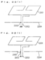
FIGS. 2(a) and 2(b) are schematic diagrams showing
other examples in which an antenna device having the same
structure as that of the above antenna device is disposed
close to a conductive base plate. That is, FIG. 2(a) shows
an antenna device in which an antenna element 201 is formed
of a linear conductor having two bent portions, the antenna
element 201 is disposed close to a conductive base plate
205 in such a manner that an antenna plane is in parallel
with the conductive base plate 205, a feeding terminal
202 is disposed at a predetermined position of the antenna
element 201, and one end portion 203 of the antenna element
201 is grounded to the conductive base plate 205. Also,
FIG. 2(b) shows an antenna device in which an antenna
element 204 is formed of a linear conductor having four
bent portions, the antenna element 204 is disposed close
to a conductive base plate 205 in such a manner that an
antenna plane is in parallel with the conductive base plate
205, a feeding terminal 202 is disposed at a predetermined
position of the antenna element 204, and one end portion
203 of the antenna element 204 is grounded to the
conductive base plate 205. In this way, the antenna
device according to this embodiment can reduce an
equipment area, and also improves the directional gain
performance since the antenna device according to the
above-described first embodiment is disposed close to the
conductive base plate 205 in such a manner that the antenna
plane is in parallel with the conductive base plate 205.
It should be noted that the number of bent portions of
the antenna element is not limited to or by the number
described in the above examples. The same is also applied
to the following embodiments.
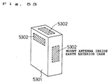
The concrete example of the antenna of FIG.2( a ) is
shown in FIG. 85. In FIG.85 an antenna element 8501 of
a linear conductor having two bent portions has such
constitution that an antenna plane is disposed in parallel
with a conductive base plate 8504 with certain space and
an one edge of the antenna element 8501 is connected to
one edge of a conductive plate 8503 which earthes the
antenna element 8501 and is provided vertical to the
conductive base plate 8504. In this embodiment the area
of a plane formed by the antenna element 8501 is
substantially equal to the area of the conductive base
plate 8504. There is a feeding terminal 8502 in the way
of the antenna element 8501.
The conductive plate 8503 has enough width against
the width of the antenna element 8501. That is the plate
8503 has such wide width so that it is not effected on
practical use by the reactance determined by a tuning
frequency of the antenna element 8501. As the result the
plate 8503 serves as an earth. If the width is not enough
the plate 8503 is integrated with the antenna element 8503
so that antenna element 8501 and the plate 8503 becomes
an antenna element as a whole which is different from the
present invention. When the wave length is 940 mm, whole
length of the antenna element 8501 is 220 mm and the width
is 2 mm and these are compact sizes. The plane of the
antenna element 8501 can be inclined against the
conductive base plate 8504 so far as the useful voltage
is generated between the antenna element 8501 and the base
plate 8504. When the area of the base plate 8504 is larger
for example four times than the area of the antenna plane,
the gain is same for vertical polarization wave and the
gain becomes less for horizontal polarization wave.
The difference between the embodiment and the prior
antenna is that for example the capability of prior
reverse F antenna becomes inferior when an antenna
element becomes near to the ground plate however the
capability of the embodiment becomes superior on the
contrary.
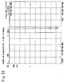
FIG.86 shows the impedance characteristics and the
VSWR characteristics of the antenna of FIG. 85. FIG. 87
shows the directional gain performance. As shown FIG. 87
the antenna of FIG. 85 has nearly circle shape directional
gain performance against a vertical polarization wave.
Now the number or shape of the antenna is not
restricted by such embodiment.
The distance between the base palate and the antenna
element is preferably 1/40 of wave length or more.
(Embodiment 2)
FIGS. 3(a) and 3(b) are schematic diagrams showing
examples of an antenna device according to a second
embodiment of the present invention. That is, FIG. 3(a)
shows an antenna device in which an antenna element 301
is formed of a linear conductor having four bent portions
to constitute a dipole antenna, a feeding terminal 302
is disposed at a predetermined position of the antenna
element 301, and one end portion 303 of the antenna element
301 is grounded. Also, FIG. 3(b) shows an antenna device
in which an antenna element 304 is formed of a linear
conductor having eight bent portions to constitute a
dipole antenna, a feeding terminal 302 is disposed at a
predetermined position of the antenna element 304, and
one end portion 303 of the antenna element 304 is grounded.
In this way, the antenna device according to this
embodiment can reduce an equipment area since the antenna
element of the dipole antenna is bent so as to be wound.
FIGS. 4(a) and 4(b) are schematic diagrams showing
other examples in which an antenna device having the same
structure as that of the above antenna device is disposed
close to a conductive base plate, respectively. That is,
FIG. 4(a) shows an antenna device in which an antenna
element 401 is formed of a linear conductor having four
bent portions to constitute a dipole antenna, the antenna
element 401 is disposed close to a conductive base plate
405 in such a manner that an antenna plane is in parallel
with the conductive base plate 405, a feeding terminal
402 is disposed at a predetermined position of the antenna
element 401, and one end portion 403 of the antenna element
401 is grounded to the conductive base plate 405. Also,
FIG. 4(b) shows an antenna device in which an antenna
element 404 is formed of a linear conductor having eight
bent portions to constitute a dipole antenna, the antenna
element 404 is disposed close to a conductive base plate
405 in such a manner that an antenna plane is in parallel
with the conductive base plate 405, a feeding terminal
402 is disposed at a predetermined position of the antenna
element 401, and one end portion 403 of the antenna element
404 is grounded to the conductive base plate 405. In this
way, the antenna device according to this embodiment can
reduce an equipment area, and also improves the
directional gain performance in the case where the antenna
device is disposed close to the conductive base plate 405
in such a manner that the antenna plane is in parallel
with the conductive base plate 405.
(Embodiment 3)
FIGS. 5(a) and 5(b) are schematic diagrams showing
examples of an antenna device according to a third
embodiment of the present invention. That is, FIG. 5(a)
shows an antenna device which is structured in such a
manner that three monopole antenna elements 501a, 501b
and 501c each having two bent portions and being different
in element length from each other are disposed on the same
plane, reactance elements 502a, 502b, 502c and 504 are
connected between the taps of the antenna elements 501a,
501b and 501c and a feeding terminal 503 and between the
feeding terminal 503 and an earth terminal 505 to adjust
an impedance, respectively. Also, FIG. 5(b) shows an
antenna device in which the antenna elements 501a, 501b
and 501c of the above antenna device shown in FIG. 5(a)
are changed to antenna elements 506a, 506b and 506c having
four bent portions.
In the above structure, the tuning frequencies of the
respective antenna elements are set at given intervals,
thereby being capable of realizing an antenna device
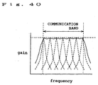
having a desired frequency band. FIG. 40 is a diagram
showing the composed frequency bands in case of an antenna
having seven antenna elements, in which the frequency band
width of one antenna element is narrow, but the frequency
characteristic of a wide frequency band can be provided
by composing the respective frequency band widths.
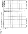
The concrete embodiments of such band composing are
shown by VSWR characteristics in FIGS. 88 to 93. It is
examples using four antenna elements which have different
tuning frequencies of
196.5MHZ(FIG.88),198.75MHZ(FIG.89),200.5MHZ(FIG.90),2
03.75MHZ(FIG.91). FIG. 92 shows the VSWR when such
antenna elements are composed with band. This shows wide
band composing. FIG. 93 shows five times extended graph
on longitudinal axis for the FIG. 92.
FIGS. 6(a) and 6(b) are schematic structural diagrams
showing examples in which an antenna device having the
same structure as that of FIG. 5(a) or 5(b) is disposed
close to a conductive base plate, respectively. These
antenna devices are structured in such a manner that the
antenna device having the same structure as that of FIG.
5(a) or 5(b) is disposed close to a conductive base plate
607 so that an antenna plane is in parallel with the
conductive base plate 607. That is, FIG. 6(a) shows an
antenna device which is structured in such a manner that
three monopole antenna elements 601a, 601b and 601c each
having two bent portions and being different in element
length from each other are disposed on the same plane so
as to be close to the conductive base plate 607, reactance
elements 602a, 602b, 602c and 604 are connected between
the taps of the antenna elements 601a, 601b and 601c and
a feeding terminal 603 and between the feeding terminal
603 and an earth terminal 605 to adjust an impedance,
respectively. Also, FIG. 6(b) shows an antenna device in
which the antenna elements 601a, 601b and 601c of the above
antenna device shown in FIG. 6(a) are changed to antenna
elements 606a, 606b and 606c having four bent portions.
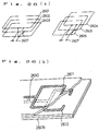
FIGS. 7(a) and 7(b) are schematic diagrams showing
other examples of an antenna device according to this
embodiment. That is, FIG. 7(a) shows the structure of an
antenna device having the same structure as that of FIG.
5(a) as described above, in which frequency band composing
reactance elements 708a and 708b are disposed between the
respective antenna elements 701a, 701b and 701c. Also,
FIG. 7(b) shows the structure of an antenna device having
the same structure as that of FIG. 5(b) as described above,
in which frequency band composing reactance elements 708a
and 708b are disposed between the respective antenna
elements 706a, 706b and 706c. In the structures of FIGS.
5(a) and 5(b), the respective reactance elements 502a,
502b and 502c are also used to compose the frequency bands.
On the other hand, in this embodiment, the adjustment of
impedance and the adjustment of frequency composition are
liable to be implemented because the function of composing
the frequency bands is separated.
FIGS. 8(a) and 8(b) are schematic diagrams showing
still other examples of an antenna device according to
this embodiment. These antenna devices are structured in
such a manner that an antenna device having the same
structure as that of FIG. 7(a) or 7(b) is disposed close
to a conductive base plate 807 so that an antenna plane
is in parallel with the conductive base plate 807. That
is, FIG. 8(a) shows the structure of an antenna device
having the same structure as that of FIG. 6(a) as described
above, in which frequency band composing reactance
elements 808a and 808b are disposed between the respective
antenna elements 801a, 801b and 801c. Also, FIG. 8(b)
shows the structure of an antenna device having the same
structure as that of FIG. 6(b) as described above, in which
frequency band composing reactance elements 808a and 808b
are disposed between the respective antenna elements 806a,
806b and 806c.
(Embodiment 4)
FIGS. 9(a) and 9(b) are schematic diagrams showing
an antenna device according to a fourth embodiment of the
present invention. That is, FIG. 9(a) shows an antenna
device which is structured in such a manner that three
dipole antenna elements 901a, 901b and 901c each having
four bent portions and being different in element length
from each other are disposed on the same plane, reactance
elements 902a, 902b, 902c and 904 are connected between
the taps of the antenna elements 901a, 901b and 901c and
a feeding terminal 903 and between the feeding terminal
903 and an earth terminal 905 to adjust an impedance,
respectively. Also, FIG. 9(b) shows an antenna device in
which the antenna devices 901a, 901b and 901c of the above
antenna device shown in FIG. 9(a) are changed to antenna
elements 906a, 906b and 906c having eight bent portions.
In the above structure, the tuning frequencies of the
respective antenna elements are set at given intervals,
thereby being capable of realizing an antenna device
having a desired frequency band.
FIGS. 10(a) and 10(b) are schematic diagrams showing
other examples of an antenna device according to this
embodiment. These antenna devices are structured in such
a manner that an antenna device having the same structure
as that of FIG. 9(a) or 9(b) is disposed close to a
conductive base plate 1007 so that an antenna plane is
in parallel with the conductive base plate 1007. That is,
FIG. 10(a) shows an antenna device which is structured
in such a manner that three dipole antenna elements 1001,
1002 and 1003 each having four bent portions and being
different in element length from each other are disposed
on the same plane so as to be close to a conductive base
plate 1007, reactance elements 1004, 1005, 1006 and 1009
are connected between the taps of the antenna elements
1001, 1002 and 1003 and a feeding terminal 1008 and between
the feeding terminal 1008 and an earth terminal 1010 to
adjust an impedance, respectively. Also, FIG. 10(b)
shows an antenna device in which the antenna devices 1001,
1002 and 1003 of the above antenna device shown in FIG.
10(a) are changed to antenna elements 1011, 1012 and 1013
having eight bent portions.
FIGS. 11(a) and 11(b) are schematic structural
diagrams showing still other examples of an antenna device
according to this embodiment. That is, FIG. 11(a) shows
the structure of an antenna device having the same
structure as that of FIG. 9(a) as described above, in which
frequency band composing reactance elements 1114, 1115,
1116 and 1117 are disposed separately at two locations
between the respective antenna elements 1101, 1102 and
1103. Also, FIG. 11(b) shows the structure of an antenna
device having the same structure as that of FIG. 9(b) as
described above, in which frequency band composing
reactance elements 1114, 1115, 1116 and 1117 are disposed
separately at two locations between the respective
antenna elements 1111, 1112 and 1113. In the structures
of FIGS. 9(a) and 9(b), the respective reactance elements
902a, 902b and 902c are also used to compose the frequency
bands. On the other hand, in this embodiment, the
adjustment of impedance and the adjustment of frequency
composition are liable to be implemented because the
function of composing the frequency bands is separated.
FIGS. 12(a) and 12(b) are schematic structural
diagrams showing still other examples of an antenna device
according to this embodiment. These antenna devices are
structured in such a manner that an antenna device having
the same structure as that of FIG. 11(a) or 11(b) is
disposed close to a conductive base plate 1207 so that
an antenna plane is in parallel with the conductive base
plate 1207. That is, FIG. 12(a) shows the structure of
an antenna device having the same structure as that of
FIG. 10(a) as described above, in which frequency band
composing reactance elements 1214, 1215, 1216 and 1217
are disposed separately at two locations between the
respective antenna elements 1201, 1202 and 1203. Also,
FIG. 12(b) shows the structure of an antenna device having
the same structure as that of FIG. 10(b) as described above,
in which frequency band composing reactance elements 1214,
1215, 1216 and 1217 are disposed separately at two
locations between the respective antenna elements 1211,
1212 and 1213.
(Embodiment 5)
FIGS. 13(a) and 13(b) are schematic structural
diagrams showing antenna devices according to a fifth
embodiment of the present invention. That is, FIG. 13(a)
shows an antenna device in which the respective antenna
elements 1301, 1302 and 1303 of three dipole antennas
different in element length from each other are formed
on a printed board 1304. Also, FIG. 13(b) shows an antenna
device in which a conductive base plate 1308 is formed
in the same structure as that of FIG. 13(a) as described
above, on a surface of the printed board 1304 opposite
to the antenna element 1320. In this way, with the
structure where the antenna elements 1301, 1302 and 1303
(1305, 1306 and 1307) and the conductive base plate 1308
are formed using the printed board, a space occupied by
the antenna can be saved, the manufacture is simplified,
and the reliability and stability of performance are also
improved.
FIGS. 14(a) and 14(b) are schematic structural
diagrams showing other examples of an antenna device
according to this embodiment. Those antenna devices are
structured such that in the same structure as that of FIG.
13(a) as described above, a conductor for composing the
frequency bands is formed on a surface of the printed board
opposite to the antenna elements so as to cross the antenna
elements. That is, FIG. 14(a) shows an antenna device in
which the respective antenna elements 1401, 1402 and 1403
of three dipole antennas different in element length from
each other are formed on a printed board 1404, and two
conductors 1405 are formed on a surface of the printed
board 1404 opposite to the surface on which the antenna
element 1410 is disposed, so as to cross the antenna
element. Also, FIG. 14(b) shows an antenna device in
which a conductive base plate 1406 is closely formed at
an opposite side of the antenna element 1410 in the antenna
device having the same structure as that of FIG. 14(a)
as described above. The conductive base plate 1406 may
be formed on the printed board using a multi-layer printed
board The above structure facilitates the manufacture
of the frequency band composing element.
(Embodiment 6)
FIGS. 15(a) and 15(b) are schematic diagrams showing
antenna devices according to a sixth embodiment of the
present invention. This embodiment is directed to an
antenna device structured such that antenna elements 1501,
1502 and 1503 are received in a recess 1505 defined in
the conductive base plate 1504. This structure
eliminates a projection of the antenna device from a car
body such as an automobile, and also the interaction of
the peripheral end portion of the antenna element 1510
with the conductive base plate 1504 enables to improve
the directional gain performance.
FIGS. 16(a) and 16(b) are schematic structural
diagrams showing other examples of an antenna device
according to this embodiment. In the antenna device shown
in FIG. 16(a), an antenna 1610 made up of antenna elements
1601, 1602 and 1603 and an antenna 1620 made up of antenna
elements 1606, 1607 and 1608 are disposed on the same plane
and also received in a recess 1605 defined in a conductive
base plate 1604. In this example, the antenna 1610 and
the antenna 1620 are made up of antennas different in size
and shape, but they may be identical in size and shape.
The antennas are disposed so that the respective feeder
sections are close to the antennas. Also, FIG. 16(b) is
a diagram showing an example in which the same antenna
is disposed close to a planer conductive base plate 1609.
FIGS. 17(a) and 17(b) are schematic structural
diagrams showing still other examples of an antenna device
according to this embodiment. In the antenna device shown
in FIG. 17(a), an upper antenna 1710 and a lower antenna
1720 which are made up of antenna elements 1701, 1702 and
1703 are disposed upper and lower, and also received in
a recess 1705 defined in a conductive base plate 1704.
In this example, the antenna 1710 and the antenna 1720
are structurally identical in size and shape, but they
may be different in size and shape. Also, FIG. 17(b) is
a diagram showing an example in which the same antenna
is disposed close to a planer conductive base plate 1706.
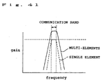
In the case where the respective antenna elements are
identical in size with each other in this way, all of the
tuning frequencies are identical with each other.
Therefore, the frequency band width of the entire antenna
device is identical with that in case of a single element,
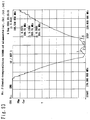
but as shown in FIG. 41, because the gains of the respective
antenna elements are accumulated in comparison with a case
in which the antenna element is single, the gain of the
entire antenna device is heightened, thereby being
capable of realizing a high-gain and high-selective
antenna.
FIGS. 18(a) and 18(b) are schematic structural
diagrams showing still other examples of an antenna device
according to this embodiment. In the antenna device shown
in FIG. 18(a), three antennas 1801, 1802 and 1803 made
up of a plurality of dipole antenna elements each having
a bent portion are formed using a multi-layer printed board
1806, and then received in a recess 1805 defined in a
conductive base plate 1804. In this example, those three
antennas 1801, 1802 and 1803 are structurally identical
in size and shape, but they may be different in size and
shape. Also, three antennas are provided in this example,
but four or more antennas may be formed into layers. FIG.
18(b) is a diagram showing an example in which the same
antenna is disposed close to a planer conductive base plate
1807. In this way, with the structure in which a plurality
of antennas are laminated using a multi-layer printed
board, an antenna high in gain and high in selectivity
can be readily obtained.
(Embodiment 7)
FIGS. 19(a) and 19(b) are schematic structural
diagrams showing two examples of an antenna according to
a seventh embodiment of the present invention. The
antenna according to this embodiment is structured such
that two linear conductors each having four bent portions
are provided for a feeder section. That is, FIG. 19(a)
shows the same antenna device as that shown in FIG. 3(b)
as described above, which includes two linear conductors
1902 and 1903 whose curving directions at the bent portions
are reverse to each other with respect to a feeder point
1901, and FIG. 19(b) shows the antenna device that includes
two linear conductors 1904 and 1905 whose curving
directions at the bent portions are identical with respect
to the feeder point 1901. These configurations enable the
antenna to be downsized on a plane and additionally enables
to realize the non-directivity.
On the other hand, FIG. 20(a) shows an antenna device
having an antenna element 2002 designed such that a length
of from a feeder section 2001 to a first bent point P is
relatively longer than a length of from the first bent
point P to a second bent point Q. Also, FIG. 20(b) shows
an antenna device having an antenna element 2002 designed
such that a length of from a feeder section 2001 to a first
bent point P is relatively shorter than a length of from
the first bent point P to a second bent point Q. The above
structures enable the antenna device to be equipped in
a slender location.
In this embodiment, two linear conductors are
provided for the feeder section, but the present invention
is not limited by or to this structure, and may be applied
to one linear conductor. Likewise, the number of bent
portions is not limited by or to those embodiments.
Also, in this embodiment, the linear conductors are
bent. Instead, they may be curved or spirally shaped.
For example, as shown in FIG. 21(a), the antenna device
may be structured to include two linear conductors 2102
and 2103 whose curving directions at the curved portions
are reverse with respect to the feeder section 2101, or
structured to include two linear conductors 2104 and 2105
whose curved directions at the curved portions are
identical with respect to the feeder section 2101. Also,
as shown in FIG. 21(b), the antenna device may be
structured to include two spiral linear conductors 2106
and 2107 whose winding directions are reverse with respect
to the feeder section 2101, or structured to include two
spiral linear conductors 2108 and 2109 whose winding
directions are identical with respect to the feeder
section 2101.
Also, in the case of producing the antenna according
to this embodiment, the antenna element may be formed by
machining a metal member, or may be formed on a substrate
by using a printed wiring. The use of the printed wiring
extremely simplifies the production of the antenna,
thereby being capable of expecting a reduction of the costs,
downsizing and an improvement in reliability.
The antennas of this embodiment can be likewise
applied to the following embodiments.
(Embodiment 8)
FIGS. 22(a) and 22(b) are schematic structural
diagrams showing examples of an antenna device according
to an eighth embodiment of the present invention. The
antenna device according to this embodiment is structured
such that an antenna element is disposed close to the
conductive base plate, and an earth terminal of the antenna
is connected to the base plate. For example, as shown in
FIG. 22(a), an antenna element 2201 is disposed close to
a base plate 2204, and its earth terminal 2203 is connected
to the base plate 2204. Although this antenna device is
similar to the structure of FIG. 4(b), they are different
in that a feeding terminal 2202 is disposed at a position
where the feeding terminal 2202 penetrates the conductive
base plate 2204. The above structure enables to obtain
desired impedance characteristic and directivity.
Also, FIG. 22(b) is structured to provide a switching
element between an earth terminal of the antenna and the
conductive base plate. As shown in the figure, a
switching element 2205 is disposed between the earth
terminal 2203 of the antenna element 2201 and the
conductive base plate 2204, and a state in which optimum
radio wave propagation is obtained is selected by
connecting or disconnecting the earth terminal 2203 and
the conductive base plate 2204. In this case, the
switching element 2205 is structured so as to be remotely
controlled so that control is made in response to a
radio wave receiving state. In this example, in the
case where the earth terminal 2203 is connected to the
conductive base plate 2204, the antenna forms a vertical
polarization antenna, but in the case where the earth
terminal 2203 is not connected to the conductive base plate
2204, it forms a horizontal polarization antenna.
Also, in the above FIG. 22(b), the feeder terminal
2202 penetrates the conductive base plate 2204, but the
present invention is not limited by or to this example.
For example, as shown in FIG. 23, the feeding terminal
2302 and the earth terminal 2303 may not penetrate the
conductive base plate 2304.
FIGS. 24(a) and 24(b) show positional relation
between a conductive base plate and an antenna according
to this embodiment. As shown in FIG. 24(a), a conductive
base plate 2402 plane and an antenna 2401 plane are so
disposed as to be in parallel with each other at a distance
h. In this case, the directivity of the antenna 2401 can
be changed to a desired direction by controlling the
distance h. Also, in the case where the antenna 2401 and
the conductive base plate 2402 approach each other, the
tuning frequency is heightened, whereas in the case where
they are away from each other, the tuning frequency is
lowered. Therefore, it may be structured such that the
distance h is controlled according to the radio wave
receiving state. For example, the control of the distance
h may be made by moving the antenna 2401 perpendicularly
with respect to the antenna plane by using a feed mechanism,
a slide mechanism not shown or the like. Alternatively,
an insulating spacer not shown is interposed between the
antenna 2401 and the conductive base plate 2402, and the
spacer is moved in parallel with the antenna plane, to
thereby adjust the mount of inserting the spacer. In this
example, in order to obtain a desired antenna performance
at the time of producing the antenna, the size of the spacer
may be decided. The spacer between the base plate and the
antenna can be made of a material low in dielectric factor
such as foam styrene.
Also, as shown in FIG. 24(b), the conductive base
plate 2402 and the antenna 2403 may be disposed
three-dimensionally such that a predetermined angle (in
this example = 90°) is defined between the conductive
base plate 2402 plane and the antenna 2403 plane. The
predetermined angle may be adjusted by a hinge mechanism
or the like, thereby enabling the control of directivity
of the antenna 2403.
Further, in this embodiment, one antenna element is
used. However, the present invention is not limited by
or to this but may use two or more antenna elements. Also,
the base plate is formed of a single conductor, but a body
of an automobile, etc., is available as the base plate.
(Embodiment 9)
FIGS. 25(a) and 25(b) are schematic diagrams showing
examples of an antenna device according to a ninth
embodiment of the present invention, in which a plurality
of antenna elements are disposed within a predetermined
area, and one antenna is structured by an antenna group
with a single feeder. As shown in FIG. 25(a), a plurality
of antenna elements 2501, 2502 and 2503 are modified in
a single feeder, and one antenna is structured by an
antenna element group. For example, each of plural
elements covers a different frequency, thereby being
capable of realizing an antenna wide in frequency band
which covers a desired frequency band as a whole. In
particular, in the arrangement shown in FIG. 25(a), since
the element length of the outer antenna 2501 is naturally
longer than the element length of the inner antenna 2503,
it is easy to set the antenna 2501 longer in element length
to a relatively low tuning frequency, and the antenna 2503
shorter in element length to a relatively high tuning
frequency, thereby being capable of structuring an
antenna that covers a wide frequency band as a whole.
Also, as shown in FIG. 25(b), the antenna device may
be structured in such a manner that a plurality of antenna
elements are provided on the same plane, but they do not
come into each other.
Also, in the case where frequency bands covered by
each of plural antenna elements are identical with each
other, the antenna efficiency can be enhanced.
Further, in order to obtain isolation between the
individual antenna elements, distances between the
respective antenna elements may be defined by intervals
necessary to obtain predetermined isolation.
Alternatively, an isolator or reflector may be connected
to the individual antenna elements.
In this embodiment, the number of antenna elements
is 2 or 3. However, the present invention is not limited
by or to this as long as the number of antenna elements
is two or more.
(Embodiment 10)
FIGS. 26(a) and 26(b) are schematic diagrams showing
examples of an antenna device according to a tenth
embodiment of the present invention. A difference of this
embodiment from the above ninth embodiment resides in that
as shown in FIG. 26(a), antenna elements 2601, 2602 and
2063, or 2604, 2605 and 2606 are so arranged to be laminated
in a direction perpendicular to a reference plane. An
arrangement state of the antenna elements on the plane
of projection is that all of the antenna elements may be
superimposed on each other as shown in the left drawing,
the antenna elements may be partially overlapped with each
other as shown in the right drawing, or they may be
separated from each other. FIG. 26(b) shows an applied
example of this embodiment, that is, a partially cut view
showing antennas 2611 and 2612 formed on a multi-layer
printed board 2609 using a printed wiring in a state where
the arrangement of the antennas on the horizontal plane
are partially overlapped. The coupling of both the
elements at a predetermined position is enabled by making
a conductor pass through a through-hole 2610.
(Embodiment 11)
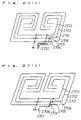
FIGS. 27(a) and 27(b) are schematic diagrams showing
examples of an antenna device according to an eleventh
embodiment of the present invention, and FIG. 27(a) shows
an example of a feeder section of an antenna in which a
plurality of antenna element groups are modified in a
single feeder. As shown in FIG. 27(a), taps 2704, 2705
and 2706 are formed at predetermined positions of the
respective antenna elements 2701, 2702 and 2703, and then
connected to a feeding terminal 2707. In this example,
the directions of those taps are identical between all
of the antenna elements, but may be set arbitrarily for
each of the antenna elements.
FIG. 27(b) shows an antenna in which electrodes
extending from a feeding terminal to the tap positions
of the respective antenna elements are made common. As
shown in the figure, taps 2704, 2705 and 2706 are formed
at predetermined positions of the respective antenna
elements 2701, 2702 and 2703, and an electrode 2708
extending from the tap positions to the feeding terminal
2707 is commonly used. With this structure, not only the
structure is simplified but also the space can be saved
by disposing the electrode 2708, for example, in parallel
with the outermost antenna element 2701.
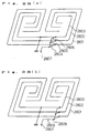
Also, FIGS. 28(a) and 28(b) show antennas providing
the taps of the respective antenna elements through
reactance elements. As shown in FIG. 28(a), the
respective antenna elements 2801, 2802 and 2803 may be
connected to a feeding terminal 2807 through reactance
elements 2804, 2805 and 2806, respectively, or as shown
in FIG. 28(b), a reactance element 2809 may be disposed
in a common electrode 2808 between the feeding terminal
2807 and the tap positions. In this example, as shown in
FIGS. 9(a) and 9(b), a reactance element may be disposed
between the feeding terminal and the earth terminal. In
this way, the use of an appropriate reactance element
enables to obtain a desired impedance, frequency band and
maximum efficiency. A variable reactance element may be
used while being adjusted as the reactance element.
(Embodiment 12)
FIG. 29 is a schematic diagram showing an example of
an antenna device according to a twelfth embodiment of
the present invention, in which a plurality of antenna
elements are disposed within a predetermined area which
is in the vicinity of a conductive base plate, one antenna
is structured by an antenna group with a single feeder,
and an earth terminal of its feeding section is connected
to the conductive base plate. As shown in FIG. 29, a
plurality of antenna elements 2901, 2902 and 2903 are
modified in a single feeder by a feeding terminal 2907
disposed to penetrate a conductive base plate 2909, one
antenna is structured by an antenna group, and an earth
terminal 2908 of the feeder section is connected to the
conductive base plate 2909. The above structure enables
a downsized and high-gain antenna to be equipped on the
plane in the vicinity of the conductive base plate.
(Embodiment 13)
FIGS. 30(a) to 30(c) are schematic diagrams showing
examples of an antenna device according to a thirteenth
embodiment of the present invention.
As shown in FIG. 30(a), an interval between opposed
portions 3001 and 3002 of an antenna element at an open
terminal side thereof is set to a predetermined distance,
and coupling of those portions is controlled to control
a tuning frequency.
Also, setting of the coupling of those opposed
portions 3001 and 3002 of the antenna element at the open
terminal side thereof may be made by providing a dielectric
3003 as shown in FIG. 30(b), or may be connected to each
other through a reactance element 3004 as shown in FIG.
30(c). In this example, the coupling may be controlled
by the dielectric 3003 being structured to be movable,
or the coupling may be controlled by a variable reactance
as the reactance element 3004.
Also, in this embodiment, the number of antenna
elements is one, but as shown in FIGS. 25(a) and 25(b),
the number of antenna elements may be two or more. Thus,
the present invention is not limited by or to this example.
(Embodiment 14)
FIGS. 31(a) to 31(c) are schematic diagrams showing
examples of an antenna device according to a fourteenth
embodiment of the present invention.
As shown in FIG. 31(a), distances between open
terminal sides 3101 and 3102 of the antenna element and
a neutral point 3103 or opposed portions 3111, 3112 in
the vicinity of the neutral point 3103 is set to a
predetermined distance, to thereby control a tuning
frequency.
Also, the setting of the coupling the open terminal
sides of the antenna element with the neutral point 3103
or the opposed portions in the vicinity of the neutral
point may be made by providing a dielectric 3104 as shown
in FIGS. 31(b) and 31(c), or may be connected to each other
through a reactance element 3105 or 3106 as shown in FIGS.
31(b) and 31(c). In this example, like the above
thirteenth embodiment, the coupling may be controlled
with the dielectric element 3104 being structurally
movable, or the coupling may be controlled with variable
reactance as the reactance elements 3101 and 3102.
Similarly, in this embodiment, the number of antenna
elements is one, but as in the antennas shown in FIGS.
25(a) and 25(b), the number of antenna elements may be
two or more. Thus, the present invention is not limited
by or to this example.
(Embodiment 15)
FIGS. 32(a) and 32(b) are schematic diagrams showing
examples of an antenna device according to a fifteenth
embodiment of the present invention. In the antenna
devices according to this embodiment, at least one linear
conductor is connected to both poles of a coil,
respectively, an earth terminal is extended from a neutral
point of the coil, a tap is formed at the respective linear
conductors or predetermined position of the coil, and a
feeding terminal is led out from the tap. As shown in FIG.
32(a), a coil 3203 has linear conductors 3201 and 3202
on both ends thereof, respectively. An earth terminal
3206 is extended from a neutral point of the coil 3203,
and a tap 3204 is formed at a predetermined position of
the linear conductor (in this example, 3202) so that a
feeding terminal 3205 is led out from the tap.
Alternatively, as shown in FIG. 32(b), a tap 3204 may be
formed at a predetermined position of the coil 3203 to
lead out the feeding terminal 3205.
The above structure enables the tuning frequency of
the antenna to be adjusted by the number of winding of
the coil, and also enables the downsizing and a wide
frequency band to be realized.
FIGS. 33(a) and 33(b) show cases in which a coil has
a plurality of linear conductors. As shown in FIG. 33(a),
a coil 3307 has a plurality of linear conductors 3301,
3302 and 3303 and 3304, 3305 and 3306 on both ends thereof,
respectively. An earth terminal 3311 is extended from a
neutral point 3310 of the coil 3307, and a tap 3308 is
formed at a predetermined position of the linear conductor
(in this example, 3304, 3305 and 3306) so that a feeding
terminal 3309 is led out from the tap. Alternatively, as
shown in FIG. 33(b), a tap 3312 may be formed at a
predetermined position of the coil 3307 to lead out the
feeding terminal 3309. In this example, the number of
one-sided linear conductors is three, but the present
invention is not limited by or to this and the number of
linear conductors may be two or more.
Also, in this embodiment, the shape of the linear
conductor that forms an antenna element is straight, but
it may have at least one bent or curved portion or be
spirally shaped. The present invention is not limited by
or to this.
(Embodiment 16)
FIG. 34 is a schematic diagram showing an example of
an antenna device according to a sixteenth embodiment of
the present invention. The antenna device according to
this embodiment is structured to include one or two groups
each consisting of a plurality of linear conductors
through coils for a feeder section. As shown in FIG. 34,
electrodes 3407 and 3408 each resulting from grouping a
plurality of linear conductors 3401, 3402, 3403 and 3404,
3405, 3406 are connected to a feeder section 3411 through
coils 3409 and 3410. The above structure enables the
tuning frequency of the antenna to be adjusted by the
number of winding of the coils and also enables the
downsizing and a wide frequency band to be realized.
(Embodiment 17)
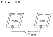
FIG. 35 is a schematic diagram showing an example of
an antenna device according to a seventeenth embodiment
of the present invention. In the antenna device according
to this embodiment, a plurality of antennas made up of
a plurality of antenna element groups are located in a
predetermined area, to conduct diversity reception where
an antenna which is optimum to a receiving state is
selected from those antennas. For example, in FIG. 35,
one antenna by which optimum radio wave propagation
is obtained is selected from two antennas 3501 and 3502
by a diversity change-over switch 3503 connected to a
feeder section. In this example, the number of antennas
is not limited to two as in this embodiment, but may be
three or more. Also, the kind of antenna is not limited
to the antenna with the shape shown in FIG. 35 but other
kinds of antennas described in the above-described
embodiments or the combination of different kinds of
antennas may be applied.
Also, in the control for selecting an optimum antenna
from a plurality of antennas, control for selecting an
antenna maximum in a receiver input may be conducted.
Alternatively, control for selecting an antenna minimum
in a multi-pass interference level may be conducted.
Further, a balanced-to-unbalanced transformer, a
mode transformer or an impedance transformer may be
connected to the respective antenna element feeder
sections or the feeder section of the antenna obtained
by converting a plurality of antenna element groups in
a single feeder according to the above embodiments 1 to
17.
(Embodiment 18)
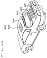
FIG. 36 is a perspective view for explanation of an
example of a location where an antenna device is equipped
according to an eighteenth embodiment of the present
invention. In this embodiment, there is described an
equipment location where an automobile is equipped with
an antenna. The equipped antenna is an antenna device
described in the above respective embodiments. The
equipment location of the antenna is, as shown in FIG.
36, a rear spoiler 3601, a trunk lid rear panel 3602, a
rear tray 3603, a roof spoiler 3604, a roof box 3606 or
a roof 3605 such as a sun roof visor.
Also, in the case where the antenna is intended to
be equipped vertically, for example, as shown in FIG. 37(a),
the antenna may be equipped on both end portions 3703 of
spoilers 3701 and 3702, an end portion 3703 of a sun visor,
etc., of an automobile, or as shown in FIG. 37(b), it may
be equipped on a pillar portion 3704. It is needless to
say that the present invention is not limited to these
examples, and the antenna can be equipped on other portions
of the automobile if they are inclined to some degree with
respect to a horizontal plane. The equipment of the
antenna on those positions enables the antenna to be liable
to receive desired polarization.
As described above, in the respective antenna devices
according to the present invention, since the antenna
plane and the car body plane which is a conductive base
plate can be disposed close to each other in parallel,
the antenna can be equipped without being projected from
the car body, and also since an area occupied by the antenna
is small, the antenna can be equipped in a small space.
Therefore, the beauty of the appearance is improved, the
occurrence of a wind sound can be suppressed, and further
problems such as a risk that the antenna is robbed, the
removal of the antenna when washing the automobile, and
so on can be eliminated.
(Embodiment 19)
FIG. 38 is a schematic diagram showing an example of
a mobile communication apparatus having an antenna device
according to a nineteenth embodiment of the present
invention. As shown in FIG. 38, an antenna 3801 which is
any one of the antennas described in the above embodiments
is equipped on the ceiling portion of a car body 3805 of
an automobile or the like. In this example, if the antenna
3801 is received in a recess 3806 formed in the ceiling
portion, there is no case in which the antenna is projected
from the outline of the car body 3805. The antenna 3801
is connected to a communication unit 3804 made up of an
amplifier 3802, a modulator/demodulator 3803 and so on
mounted inside of the car body 3805.
(Embodiment 20)
FIGS. 39(a) and 39(b) are schematic diagrams showing
examples of a portable telephone having an antenna device
according to a twentieth embodiment of the present
invention. FIG. 39(a) shows an example in which a
conductive shield case 3902 disposed inside of a resin
case 3901 of the portable telephone is utilized as a
conductive base plate, and an antenna 3903 is disposed
on an inner side surface of the case 3901 so as to be in
parallel with the shield case 3902. Also, FIG. 39(b)
shows an example in which an antenna 3904 is disposed on
an outer top portion of the resin case 3901 of the portable
telephone, and a conductive base plate 3905 is disposed
on an inner portion opposite to the antenna 3904 across
the case 3901. In this example, the top portion of the
shield case 3902 is not employed as the conductive base
plate because normally there is a small area. In both of
FIGS. 39(a) and 39(b), the antenna to be used may be, in
particular, an antenna the number of bent portions of which
or the number of windings is large because such an antenna
can be readily downsized among the antennas described in
the above respective embodiments.
The use of the above structure enables
electromagnetic wave interference on a human body to be
reduced without lowering the antenna efficiency if the
conductive base plate is at the side of the human body
because the directional gain of the conductive base plate
side is extremely smaller than that of the antenna side.
In the above eighteenth embodiment, there is
described the example in which the antenna device is
equipped on the automobile. However, the present
invention is not limited to this example, and may be
applied to other movable bodies such as an aircraft or
ship. Alternatively, the antenna device is not limited
to the movable bodies but may be equipped on a road surface,
a shoulder, a fare gate, within a tunnel of a traffic road
such as a superhighway, and also a wall surface and window
of a building, etc.
Also, in the above nineteenth embodiment, the antenna
device for the movable communication unit is described
as an example. However, the present invention is not
limited to this embodiment. For example, the present
invention is available to a device that receives or
transmits a radio wave such as a television, a radio
cassette and a radio unit.
Further, in the above twentieth embodiment, the
portable telephone is described as an example. However,
the present invention is not limited to this. For example,
the present invention is also applicable to other portable
radio unit such as PHS, a pocket bell or a navigation
system.
(Embodiment 21)
FIGS. 42(a) and 42(b) are schematic structural
diagrams showing an antenna device according to a
twenty-first embodiment of the present invention. That
is, FIG. 42(a) shows an antenna device that is a monopole
wide frequency band antenna, which is made up of a main
antenna element 4202 one end of which is connected to a
ground 4204, an antenna element 4201 disposed close to
the main antenna element 4202, longer in element length
than the antenna element 4202 and having both ends not
grounded, and an antenna element 4203 shorter in element
length than the antenna element 4202 and having both ends
not grounded. The main antenna element 4202 has a tap
which is connected to a feeder point 4206 through an
impedance adjustment reactance element 4205. Also, FIG.
42(b) shows an example in which the antenna elements 4201,
4202 and 4203 of the antenna device shown in FIG. 42(a)
are formed on the printed board 4207 by using a printed
wiring.
FIGS. 43(a) and 43(b) show examples in which the
antenna device of the above embodiment is of the dipole
type. That is, FIG. 43(a) shows an antenna device that
is a dipole wide-frequency band antenna, which is made
up of a main antenna element 4302 a center portion of which
is connected to a ground 4304, an antenna element 4301
disposed close to the main antenna element 4302, longer
in element length than the antenna element 4302 and not
grounded anywhere, and an antenna element 4303 shorter
in element length than the antenna element 4302 and not
grounded anywhere. The main antenna element 4302 has a
tap which is connected to a feeder point 4306 through an
impedance adjustment reactance element 4305. Also, FIG.
43(b) shows an example in which the antenna elements 4301,
4302 and 4303 of the antenna device shown in FIG. 43(a)
are formed on the printed board 4307 by using a printed
wiring.
The above structure makes the frequency band wide,
the gain high and the adjustment easy with a simple
structure.
In the above embodiment, the antenna element shorter
than the main antenna element and the antenna element
longer than the main antenna element which are disposed
close to the main antenna element are formed by one piece,
respectively. However, the present invention is not
limited by this example, and two or more shorter antenna
elements and longer antenna elements may be provided,
respectively.
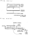
(Embodiment 22)
FIGS. 44(a) and 44(b) are schematic structural
diagrams showing antenna devices according to a
twenty-second embodiment of the present invention. That
is, FIG. 44(a) is similar to the antenna device in which
the conductive base plate is disposed close to the antenna
element as described, for example, in FIG. 10(a) and 10(b),
but the antenna device of FIG. 44(a) is different from
such antenna device in that the size of the conductive
base plate 4404 disposed close to the antenna elements
4401, 4402 and 4403 is set to be substantially equal to
or smaller than that of the outermost antenna element 4401.
This structure improves the horizontal polarization gain
in comparison with a case in which the conductive base
plate is larger than the antenna element.
Also, FIG. 44(b) shows an example in which the antenna
device shown above in FIG. 44(a) is received in a recess
formed in, for example, a movable body, a communication
unit case, a house wall, other device cases, etc., in which
the antenna earth (conductive base plate) 4404 is not
connected to the case earth. This structure enables a
high gain to be obtained in both of the horizontal and
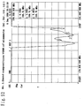
vertical polarizations. The FIG. 94 shows a directional
gain performance of the antenna for the vertical
polarization wave. The distance between the antenna
earth and case earth(namely separate distance)
are (a)10mm,(b)30mm,(c)80mm,(d)150mm respectively and
they shows that the gain becomes higher according to the
distance becomes smaller. That is the capability becomes
improved as the antenna earth and the case earth comes
nearer. Further in this example in order to prevent a
protrusion of the antenna from the outside case, the
antenna earth 4404 is installed within a concave part which
is formed at such cases of movile body, transmission case,
house wall, and soon. But the capability of the antenna
is same even when the antenna element is provided to with
suitable short distance the plane surface of a case earth.
Such embodiment is included in the claimed present
invention.
Now in the above embodiment balance type is used
as the antenna element but unbalance type antenna element
can be used.
(Embodiment 23)
FIGS. 45(a) and 45(b) are schematic structural
diagrams showing examples of an antenna device according
to a twenty-third embodiment of the present invention.
This embodiment shows an example of how close the
conductive base plate should be disposed to the antenna
element, and FIG. 45(a) shows an example in which there
is provided one antenna element. That is, a distance h
between the antenna element 4501 (accurately, an antenna
earth connection portion) and a conductive base plate 4502
is set within the limit of 0.01 to 0.25 times (that is,
0.01λ to 0.25λ) as large as the wavelength λ in the
resonance frequency f of the antenna. This structure
makes the gain high and the adjustment easy.
Also, FIG. 45(b) shows a case in which four antenna
elements are provided, and antenna elements 4503, 4504,
4505 and 4506 are disposed at different distances from
a conductive base plate 4507, respectively. As shown in
FIG. 45(b), in the case where the element length is
different among the respective antenna elements, as the
element length is shortened, the resonance frequency of
the antenna element is heightened more, and the wavelength
is shortened. Accordingly, a distance h1 of the antenna
element 4506 shortest in element length is set to be the
smallest, a distance h2 of the antenna element 4503 longest
in element length is set to be the largest, and a distance
of the intermediate antenna elements 4504 and 4505 may
be set according to the wavelength in the resonance
frequency of the respective antenna elements. In this
case, the respective distances between the respective
antenna elements 4503, 4504, 4505, 4506 and the conductive
base plate 4507 are set so as to satisfy the conditions
of 0.01 to 0.25 times (that is, 0.01λ to 0.25λ) with respect
to the respective wavelengths in the resonance frequency
of the respective antenna elements as described above.
(Embodiment 24)
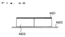
FIG. 46 is a schematic structural diagram showing an
example of an antenna device according to a twenty-fourth
embodiment of the present invention. In this embodiment,
a high dielectric material is provided between an antenna
element 4601 and a conductive base plate 4602. Therefore,
this embodiment is applicable to the structure of the
embodiments in which the conductive base plate is disposed
close to the antenna element among the above-described
antenna devices. In this example, the provision of the
high dielectric material between the antenna element and
the conductive base plate enables a distance between the
antenna element and the conductive base plate to be
equivalently reduced.
(Embodiment 25)
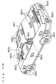
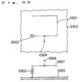
FIG. 47 is a perspective view showing an example in
which an antenna device is applied to a car body according
to a twenty-fifth embodiment of the present invention.
That is, any antenna devices of the above-described
embodiments according to the present invention are
located at four positions of a car body pillar portion
4701 at the front, rear, right and left sides of an
automobile and at one position of a roof portion, that
is, at five positions in total, to thereby provide a
diversity structure by those plane antennas. This
structure enables excellent transmission and reception
with respect to both of the horizontal and vertical
polarizations. In this example, there are five positions
at which the antennas are located, but the locations are
not limited by this.
(Embodiment 26)
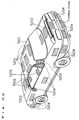
FIG. 48 is a perspective view showing an example in
which locations where an antenna device is equipped are
applied to the respective parts of a car body according
to a twenty-sixth embodiment of the present invention.
That is, any antenna devices of the above-described
embodiments according to the present invention are fitted
to any location or a plurality of locations which are on
the surface of a car body 4801 where the antenna device
can be located, such as a roof panel, a bonnet, a body
pillar portion, a body side, a bumper, a tire wheel or
a floor of the car body 4801 of an automobile. In FIG.
48, an antenna 4802 is equipped on a location where the
antenna plane is substantially horizontal, an antenna
4803 is equipped at a location where the antenna plane
is obliquely inclined, and an antenna 4804 is equipped
at a location where the antenna plane is substantially
vertical. The figure shows appropriate locations where
the antenna should be equipped, and it is unnecessary to
equip the antenna on all the locations. Also, it is
needless to say that the antenna may be disposed at
locations other than those shown in the figure. Also, the
kind of the automobile is not limited by a motor car as
shown, but an automobile such as a bus or a motortruck
is also acceptable.
An antenna 4805 is located such that the antenna plane
is horizontal, and in particular, located on a rear side
(under side) of the floor, and the directional
characteristic is directed to a road surface. Therefore,
the antenna 4805 is suitable for communication with a
radio wave source located on (or buried under) a road
used for communication, detection of a location where the
car body is situated, etc.
As usual, a radio wave used for a TV or FM
broadcasting is a radio wave that mainly includes a
horizontal polarization, and a radio wave used for
a portable telephone, a radio communication unit, etc.,
is a radio wave that mainly includes a vertical
polarization. It is determined whether it is suitable for
the horizontal polarization or the vertical polarization
according to a direction of locating the antenna. As
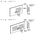
shown in FIG. 49(a), in an unbalanced three-element
antenna 4902 disposed in parallel with a face of a vertical
conductive base plate 4901 which is a part of the car body
4801 so that an earth terminal thereof is connected to
the conductive base plate 4901, since an electric field
is horizontal as shown in the right figure, and the
sensitivity can be enhanced with respect to the horizontal
polarization, it is effective as a horizontal
polarization antenna. This can be realized by equipping
the antenna 4804 of FIG. 48 on the locations indicated
by the antenna 4804. Also, because the antenna 4802 is
an antenna disposed in parallel with a horizontal face
of the car body 4801, its electric field is vertical so
that the sensitivity becomes high with respect to the
vertical polarization. Therefore, it is effective as the
vertical polarization antenna. Further, an antenna 4803
is located so as to be obliquely inclined, has a balanced
sensitivity between the horizontal polarization and the
vertical polarization according to the inclined degree,
and can be used, hardly depending on the polarization
direction. FIG. 49(b) shows an example of a balanced
antenna which is effective as the horizontal polarization
antenna as in the above description.
(Embodiment 27)
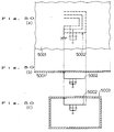
FIGS. 50(a) to 50(c) are schematic diagrams showing
the structures of an antenna device according to a
twenty-seventh embodiment of the present invention. A
difference of the antenna device according to this
embodiment from the above-described antenna devices
resides in that a direction of transmitting and receiving
a radio wave is not at the antenna element side but
at the conductive base plate side. As shown in FIG. 50(a),
a three-element antenna 5002 is disposed in parallel with
a conductive base plate 5001 at a given interval, an earth
end portion of the antenna 5002 is connected to the
conductive base plate 5001, and the conductive base plate
5001 side is directed outward. In FIG. 50(b), this
antenna exhibits a symmetric directional characteristic
with respect to an upper side of the conductive base plate
5001 region (side opposite to the antenna 5002) that
corresponds to a region covered with the antenna 5002
surface and a lower side thereof with respect to the
antenna 5002. For that reason, even if a direction of
arranging the antenna 5002 and the conductive base plate
5001 is reverse to that of the conventional arrangement,
the same effects as those of the antennas as described
in the above embodiments can be obtained. Further, as
shown in FIG. 50(c), even if the conductive base plate
5003 is shaped in a closed case, the same characteristic
is obtained, and even if electricity is fed to the antenna
5002 inside of the conductive base plate 5003,
communication is enabled to the exterior through the
conductive base plate 5003.
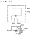
FIG. 51 shows an example in which the unbalanced
antenna device of FIG. 50 is changed to a balanced antenna
device with the same effects as those described above.
Also, FIG. 52 shows an example in which an antenna
device of this embodiment is applied to the respective
locations of a car body as shown in FIG. 48. In FIG. 52,
like FIG. 48, an antenna 5202 is equipped on a location
where the antenna plane is substantially horizontal, an
antenna 5203 is equipped at a location where the antenna
plane is obliquely inclined, and an antenna 5204 is
equipped at a location where the antenna plane is
substantially vertical. Also, the antenna 5205 is
located so that the antenna plane is horizontal, and in
particular located inside of a floor, which is suitable
for communication with a radio wave source located
on a road as in the case of FIG. 48. Although all of those
antennas are disposed inside of the car body 5201, the
same performance as that in the case where they are located
on the body surface can be realized for the above reason,
and since the antennas are not exposed to the exterior
of the car body, it is greatly advantageous from the
viewpoints of the beauty, damage, theft, etc. Further,
as shown in FIG. 52, the antenna device can be equipped
even on locations to which the antenna cannot be normally
fitted, such as a back mirror, a room sun visor or a number
plate by using its interior.
FIG. 53 is a perspective view showing an example in
which an antenna device is applied to a portable telephone
according to this embodiment, in which an antenna 5302
is located inside of an earth exterior case 5301 made of
a conductor, and the antenna earth is connected to the
earth exterior case 5301. With this structure, the
antenna can be used as in the case where the antenna is
located outside of the earth exterior case 5301, and the
antenna is not exposed to the exterior, thereby leading
to an advantage in handling. In this example, the
portable telephone is described as an example, but the
present invention is also applicable to TV, PHS, other
radio units, etc.
FIG. 54 is a perspective view showing an example in
which an antenna device is applied to a general house
according to this embodiment. That is, an antenna 5402
is located inside of a conductive door of a house 5401,
an antenna 5403 is located inside of a conductive window
(for example, a shutter), an antenna 5404 is located inside
of a conductive wall, and an antenna 5405 is located inside
of a conductive roof. In this way, if the antenna is
located using the inside of a construction which is a
conductor of a house 5401, since the antenna is not exposed
to the exterior, a damage or deterioration by wind and
rains can be prevented, leading to a long lifetime.
Even in the case where the house is a construction
which is not a conductor, the antenna can be readily
equipped if a conductor is fitted to the outside of only
a location where the antenna is equipped.
(Embodiment 28)
FIGS. 55(a) and 55(b) are schematic diagrams showing
the structure of an antenna device according to a
twenty-eighth embodiment of the present invention. This
embodiment is structured in such a manner that a conductive
base plate 5501 and an antenna 5502 located close to the
conductive base plate 5501 in parallel can be rotated about
an axis indicated by a dashed line as a center at the same
time. As shown in FIG. 55(a), because an electric field
is horizontal as shown in the right drawing in a state
where the antenna 5502 is vertical, the sensitivity
becomes high with respect to the horizontal polarization.
On the other hand, as shown in FIG. 55(b), because an
electric field is vertical as shown in the right drawing
in a state where the antenna 5502 is horizontal, the
sensitivity becomes high with respect to the vertical
polarization. The antenna can be adjusted to an optimum
direction according to the polarization state. It is
needless to say that it may be set to a state where the
antenna is obliquely inclined. FIG. 95 shows the
directional gain performance of the conditions of FIG.
55( a ) and the FIG. 96 shows the directional gain
performance of the conditions of FIG.55(b). As apparent
from these FIGs. 95,96, the antenna has high sensitivity
against a horizontal polarization wave when the antenna
is provided vertically and the antenna has high
sensitivity against a vertical polarization wave when the
antenna is provided horizontally.
In this example, as a method of rotating the
conductive base plate 5501 and the antenna 5502, there
are a manual type in which a handle may be rotated by hands,
and an automatic type using a drive unit such as a motor.
FIG. 56(a) is a schematic diagram showing the
structure of an antenna device for realizing the above
effect without rotating the antenna. That is,
ferroelectrics 5603 are disposed between a conductive
base plate 5601 and an antenna 5602 so that an antenna
5602 is sandwiched. With this structure, as shown in the
right drawing of FIG. 56(b), because an electric field
between the conductive base plate 5604 and the antenna
5605 is expanded horizontally through the ferroelectrics
5606, a vertical component is reduced whereas a horizontal
component is increased in comparison with a case where
there is no ferroelectrics shown in the left drawing. In
this way, the antenna can be set to a vertical polarization
mode or a horizontal polarization mode according to the
presence/absence of the ferroelectrics. In the case
where the antenna is located in a vertical state, the
effect is reverse to the above. Two kinds of
ferroelectrics 5603 which are mounted and not mounted,
respectively, when manufacturing may be prepared.
Alternatively, the ferroelectrics may be designed so as
to be removably attached by the provision of a removably
attachment groove or the like.
(Embodiment 29)
FIGS. 57(a) to 57(c) are diagrams showing examples
of the structure of an antenna device according to a
twenty-ninth embodiment of the present invention. The
antenna devices according to the above-described
embodiments use an element bent so as to save a space for
location. On the other hand, in this embodiment, there
is used a straight linear element or an element shaped
along the configuration of a structural member so that
the element can be located on a slender structural member
fitted on an automobile or the like.
FIG. 57(a) shows an example in which a straight linear
antenna 5702 consisting of three elements is disposed
close to the surface of a slender plate-like conductive
base plate 5701. FIG. 57(b) shows an example in which a
straight linear antenna 5704 consisting of three elements
is disposed close to the surface of a pipe-shaped
conductive base plate 5703 in such a manner that the
respective elements are apart from the conductive base
plate 5703 at given distances. FIG. 57(c) shows an
example in which a straight linear antenna 5706 consisting
of three elements is disposed close to the surface of a
rectangular cylindrical conductive base plate 5705 in
such a manner that the respective elements are apart from
the conductive base plate 5705 at given distances.
Also, FIGS. 58(a) to 58(c) are schematic diagrams
showing examples in which, in the case where the
configuration of the conductive base plate is curved or
bent in the examples of FIGS. 57(a) to 57(c), elements
are curved or bent along that configuration, and FIG. 58(a)
shows an example in which an antenna 5802 consisting of
three elements is disposed close to the surface of a curved
pipe-shaped conductive base plate 5801, in which the
respective elements are curved in the same manner as the
curved pipe-shaped conductive base plate 5801 and apart
from the conductive base plate 5801 at given distances.
FIG. 58(b) shows an example in which an antenna 5804
consisting of three elements is disposed close to the
surface of a bent rectangular cylindrical conductive base
plate 5803, in which the respective elements are bent in
the same manner as the conductive base plate 5803 and apart
from the conductive base plate 5803 at given distances.
FIG. 58(c) shows an example in which an antenna 5806
consisting of three elements is disposed close to the
surface of a bent plate-like conductive base plate 5805,
in which the respective elements are bent in the same
manner as the conductive base plate 5805.
Also, FIG. 59(a) shows an example of an antenna 5902
disposed along the periphery of the surface of a
cylindrical conductive base plate 5901, and FIG. 59(b)
shows an example of an antenna 5904 disposed along the
periphery of the surface of a spherical conductive base
plate 5903.
In this embodiment, the antenna is located outside
of the structural member which is a conductive base plate.
However, the present invention is not limited by or to
this, but the antenna may be located inside of a
plate-shaped member or in the interior of a cylindrical
member, etc.
FIGS. 63 and 65 are diagrams showing an applied
example of an antenna device according to this embodiment.
FIG. 63 shows an example in which an antenna 6302 is located
on the surface of a slender roof rail 6303 on the roof
of a car body 6301, and FIG. 65 shows an example in which
an antenna 6502 is located in the interior of a slender
roof rail 6503 on the roof of a car body 6501.
Likewise, FIGS. 64 and 66 are diagrams showing an
applied example of an antenna device according to this
embodiment. FIG. 64 shows an example in which an antenna
6403 is located on the surface of a slender roof box 6402
on the roof of a car body 6401, and FIG. 66 shows an example
in which an antenna 6603 is located in the interior of
a slender roof box 6602 on the roof of a car body 6601.
(Embodiment 30)
FIGS. 60(a) and 60(b) are schematic diagrams showing
examples of the structure of an antenna device according
to a thirtieth embodiment of the present invention. In
the antenna device according to this embodiment, in the
structure having an antenna 6002 consisting of three
elements which are relatively longer in element length
and an antenna 6003 consisting of three elements which
are relatively shorter in element length with reference
to an earth end portion connected to a conductive base
plate 6001, feeder points A6005 and B6004 are disposed
on those antennas 6002 and 6003, respectively. As shown
in FIG. 60(c), the shorter antenna 6003 is tuned to a
relatively high-frequency band A whereas the longer
antenna 6002 is tuned to a relatively low-frequency band
B, thus being capable of realizing an antenna adaptable
to two tuning frequency bands by a single antenna. The
feeder points A6005 and B6004 may be connected to each
other.
FIGS. 61(a) and 61(b) are examples of an unbalanced
antenna having two tuning bands. This antenna consists
of four elements having one end connected to a conductive
base plate 6101 and disposed close to the conductive base
plate 6101. A feeder point B6104 is set to an antenna 6102
of two elements relatively longer in element length among
those four elements, and a feeder point A6105 is set to
an antenna 6103 of two elements relatively shorter in
element length. With this arrangement, as shown in FIG.
61(c), the antenna is adaptable to two tuning bands of
a high-frequency band A and a low-frequency band B as in
the above example. The feeder points A6005 and B6004 may
be connected to each other.
FIGS. 62(a) and 62(b) show examples of a balanced
antenna having two tuning bands. This antenna consists
of four elements whose center points are connected to a
conductive base plate 6201 and disposed close to the
conductive base plate 6201. A feeder point B6204 is set
to an antenna 6202 of two elements relatively longer in
element length among those four elements, and a feeder
point A6205 is set to an antenna 6203 of two elements
relatively shorter in element length. With this
arrangement, as shown in FIG. 62(c), the antenna is
adaptable to two tuning bands of a high-frequency band
A and a low-frequency band B as in the above example. The
feeder points A6005 and B6004 may be connected to each
other.
As described above, in this embodiment, since there
can be provided a high-performance antenna device that
suppresses a space where the antenna device is equipped
to the minimum, and is adaptable to a plurality of tuning
bands, it is also applicable to a small location such as
an automobile or a portable telephone.
In this embodiment, two tuning bands are set.
However, the present invention is not limited by or to
this, for example, may be structured so as to be adaptable
to three or more bands. In this case, a plurality of
antennas having element lengths corresponding to the
respective tuning bands may be provided in such a manner
that feeder points are set to the respective antennas.
(Embodiment 31)
FIG. 67 is a schematic diagram shoving an example of
an antenna device according to a thirty-first embodiment
of the present invention. The antenna device according
to this embodiment is structured such that a coil 6703
is provided on the way of a U-shaped antenna element 6701
which is disposed close to a conductive base plate 6702,
and one end of the antenna element 6701 is connected to
the conductive base plate 6702. Also, a feeder section
6704 is disposed on the way of the antenna element 6701
between the coil 6703 and the conductive base plate 6702.
With this structure, a current is concentrated in the coil,
and the antenna device can be downsized without any change
of the gain. For example, a portion of the antenna element
is constituted by a strip line, an area of the antenna
is reduced to 1/4. Also, the frequency band width is
narrowed to sharpen the frequency band characteristic.
Also, FIG. 68 shows an example in which two antenna
elements structured as shown in FIG. 67 are connected in
parallel so as to compose the frequency bands. That is,
two antenna elements 6801a and 6801b different in
frequency band (length) on the way of which coils 6803a
and 6803b are inserted are disposed in parallel, and one
end of the respective antenna elements is connected to
a conductive base plate 6802. The respective antenna
elements 6801a and 6801b are commonly connected to a feeder
section 6804 through reactance elements 6805a and 6805b,
respectively. With this structure, the bands of two
antenna elements can be composed, and in addition to the
above effects , the antenna device can be broadened in
frequency band.
(Embodiment 32)
FIG. 69 is a schematic diagram showing an example of
the structure of an antenna device according to a
thirty-second embodiment of the present invention. The
antenna device according to this embodiment is structured
in such a manner that a coil 6903 is inserted between one
end of a U-shaped antenna element 6901 disposed close to
a conductive base plate 6902 and the conductive base plate
6902, and the other end of the coil 6903 is grounded to
the conductive base plate 6902. Also, a feeder section
6904 is disposed on the way of the antenna element 6901.
With this structure, likewise as the above-described
thirty-second embodiment, a current is concentrated in
the coil, and the antenna device can be downsized without
any change of the gain.
FIG. 70 shows an example in which two antenna elements
structured as shown in FIG. 69 are connected in parallel
so as to compose the frequency bands. That is, two antenna
elements 7001a and 7001b different in frequency band
(length) are disposed in parallel, and one ends of the
respective antenna elements are commonly connected to one
end of a coil 7003, and the other end of the coil 7003
is connected to a conductive base plate 7002. The
respective antenna elements 7001a and 7001b are commonly
connected to a feeder section 7004 through reactance
elements 7005a and 7005b, respectively. With this
structure, the bands of two antenna elements can be
composed, and in addition to the above effects, the antenna
device can be broadened in frequency band. Also, since
the coil is commonly used for two antenna elements, the
structure is simplified with one coil.
(Embodiment 33)
FIG. 71 is a schematic diagram showing an example of
the structure of an antenna device according to a
thirty-third embodiment of the present invention. A
difference of this invention from the above thirty-second
embodiment resides in that as shown in FIG. 71, an
insulator 7105 is disposed on a conductive base plate 7102,
and an antenna element 7101 and a coil 7103 are connected
to each other on the insulator 7105. This structure
allows the equipment of the coil 7103 to be facilitated,
is convenient for the mounting of the coil, and the coil
can be stably located. Also, FIG. 72 shows an example of
the structure in which frequency bands are composed by
two antenna elements 7201a and 7201b. It is complicated
to connect the antenna elements and the coil 7203 because
the number of antenna elements is increased. However,
since a connection point is provided on the insulator 7205
which is disposed on the conductive base plate 7202, the
connection between the antenna element and the coil is
further facilitated.
(Embodiment 34)
FIG. 73 is a schematic diagram showing an example of
the structure of an antenna device according to a
thirty-fourth embodiment of the present invention. In
the antenna device according to this embodiment, a coil
portion is divided into two sections, and antenna elements,
the coil and soon are connected using two insulators 7305a
and 7305b disposed on a conductive base plate 7302. That
is, one end of a U-shaped antenna element 7301 disposed
close to the conductive base plate 7302 and one end of
a coil 7303a are connected to each other on the insulator
7305a. The other end of the coil 7303a, one end of another
coil 7303b and a feeder section 7304 are connected to each
other on another insulator 7305b, and the other end of
the coil 7303b is grounded to the conductive base plate
7302. Also, FIG. 74 shows an antenna device for composing
the frequency bands using two antenna elements 7401a and
7401b, in which an antenna element, a coil and a feeder
section are connected as in the structure of FIG. 73.
This structure facilitates the connection of the
antenna to another circuit component since the terminal
of the feeder section is provided on a circuit substrate.
(Embodiment 35)
FIG. 75 is a schematic diagram showing an example of
the structure of an antenna according to a thirty-fifth
embodiment of the present invention. The antenna device
according to this embodiment is structured such that a
zigzag-shaped pattern 7503 is inserted in an antenna
element 7501 instead of the coil in the structure of FIG.
67. The structure using the coil is expanded three-dimensional
in shape whereas the use of this pattern 7503
enables the pattern to be formed on the same plane as that
of the antenna element 7501, and the antenna can be
manufactured by a print wiring method or the like. Also,
FIG. 76 shows a band composing antenna device using two
antenna elements 7601a and 7601b, in which zigzag-shaped
patterns 7603a and 7603b are inserted in the respective
antenna elements 7601a and 7601b. The pattern may be a
saw-tooth like pattern, etc., as shown in FIG. 78(c).
(Embodiment 36)
FIG. 77 is a schematic diagram showing an example of
the structure of an antenna according to a thirty-sixth
embodiment of the present invention. The antenna device
according to this embodiment is structured such that the
entire antenna element 7701 disposed close to a conductive
base plate 7702 is formed in a zigzag-shaped pattern, and
one end of the antenna element 7701 is connected to one
end of a coil 7703 the other end of which is grounded.
A feeder section 7704 is disposed on the way of the
zigzag-shaped antenna element. According to this
structure, although the loss is increased, the antenna
device can be further downsized to, for example, 1/6 or
1/8. Also, the antenna device may be in the form of a
pattern as shown in FIGS. 78(b) and 78(c) except for the
above case. FIG. 78(b) shows a three-dimensionally coil
shaped one.
(Embodiment 37)
FIG. 79 is a schematic diagram showing an example of
the structure of an antenna according to a thirty-seventh
embodiment of the present invention. In the antenna
device according to this embodiment, an insulator 7904
is disposed on a conductive base plate 7902, a lead wire
7905 drawn out from an antenna element 7901 and a feeder
section 7903 are connected to each other on the insulator
7904. This structure facilitates the connection of the
feeder section 7903 and other circuit components disposed
on the circuit substrate because the feeder section 7903
is provided on the circuit substrate.
Also, FIG. 80 shows the structure in which a
through-hole 8005 is defined in a conductive base plate
8002, and an insulator 8004 is disposed on the conductive
base plate 8002 opposite to a side where an antenna element
8001 exists. Then, a lead wire 8006 drawn out from the
antenna element 8001 penetrates the through-hole 8005 and
the insulator 8004 so as to be connected to a feeder section
8003 on the insulator 8004. As a result, since a circuit
component is connected to the lead wire on a back side
of the conductive base plate 8002, it is convenient to
deal with other circuit components which is connected to
the feeder section 8003 more than the structure of FIG.
79.
Also, FIG. 81 shows an example where, in the structure
of FIG. 80, another conductive plate is provided on the
back surface of a conductive base plate (a surface opposite
to the antenna element), and a variety of circuit
components are mounted on the provided conductive plate.
That is, a through-hole 8104 through which a lead wire
8111 drawn out from an antenna element 8101 passes is
formed in a conductive base plate 8102 and a conductive
plate 8105, and an insulator 8103 is disposed on the
conductive plate 8105 side of the through-hole 8104.
Further, insulators 8106 of required number are disposed
on the surface of the conductive plate 8105 for connection
of various circuit components. Then, the lead wire 8111
is connected to the insulator 8103 through the
through-hole 8104, and circuit components 8107 to 8110
are connected onto the insulator 8103 and the respective
insulators 8106.
This structure enables the circuit to be disposed
immediately close to the antenna, and shield between the
antenna and the circuit is readily made using the
conductive plate, which is effective to downsize the
equipment.
Also, FIG. 82 shows an example of the structure in
which a circuit component is disposed on the antenna
element side. That is, there are provided insulators 8203
of required number for connecting a lead wire 8205 drawn
out from an antenna element 8201 onto a conductive base
plate 8202, and insulators 8206 of required number for
connecting various circuit components. Further, a
conductive shield case 8204 is disposed on the conductive
base plate 8202 so as to shield the antenna element 8201
from the conductive base plate 8202, and a through-hole
8207 through which the lead wire 8205 passes is formed.
Then, the lead wire 8205 is connected onto the insulator
8203 through the through-hole 8207, and circuit
components 8208 to 8210 are connected onto the insulator
8203 and the respective insulators 8206. One end of the
antenna element 8201 is grounded to the shield case 8204.
According to this structure, although the circuit is
received between the antenna element and the conductive
base plate, the circuit is shielded by a shield case, and
the device can be downsized more than the case of FIG.
81.
(Embodiment 38)
FIG. 83 is a schematic diagram showing an example of
the structure of an antenna according to a thirty-eighth
embodiment of the present invention. The antenna device
according to this embodiment is designed such that an
antenna element 8301 is patterned on one surface of an
insulating plate 8305, and one end portion 8307 of the
antenna element 8301 penetrates an insulating plate 8305.
A lead wire 8303 that penetrates the insulating plate 8305
is drawn out from the halfway of the antenna element 8301,
a lead wire 8306 patterned on the opposite surface of the
insulating plate 8305 in parallel with the antenna element
8305 is connected to the lead wire 8303, and a feeder
section 8304 is connected to the lead wire 8306. The
feeder section 8304 is disposed at a position close to
the one end portion 8307 of the antenna element 8301. Then,
the insulating plate 8305 and the conductive base plate
8302 are disposed in parallel with each other, and the
one end portion 8307 of the antenna element 8301 is
connected to the conductive base plate 8302.
According to this structure, since the ground portion
of the antenna element is close to the feeder section,
it is convenient for a case where a coaxial cable is
connected.
(Embodiment 39)
FIG. 84 is a schematic diagram showing an example of
the structure of an antenna according to a thirty-ninth
embodiment of the present invention. The antenna device
according to this embodiment is designed such that another
conductive base plate 8404 is disposed on a large
conductive base plate 8402 through an insulating plate
8405, and an antenna element 8401 is disposed close to
the conductive base plate 8404. In this example, one end
of the antenna element 8401 is grounded to the conductive
base plate 8404. Also, it is preferable that the size of
the conductive base plate 8404 is made equal to an area
of the antenna element 8401. The conductive base plate
8402 is, for example, an automobile, an electric train
body, a metallic case portion of a receiver or
communication unit, a metallic structural portion of a
house, etc. The equipping method may be outside or inside
of a car room.
According to this structure, the angle of elevation
having an maximum gain becomes nearly horizontal and
proper for a communication radio wave (vertical
polarization wave) coming laterally.
It is needless to say that the antenna devices
according to the above-described thirty-first to
thirty-ninth embodiments can be also equipped on the
locations described with reference to FIGS. 36, 47, 48,
52, 53, 54, etc.
Also, in the above-described thirty-first to
thirty-ninth embodiments, the number of antenna elements
is one or two. The present invention is not limited by
or to this, and the number of antenna elements may be three
or more.
Further, in the above-described thirty-first to
thirty-ninth embodiments, the antenna element is U-shaped.
The present invention is not limited by or to this, and
the antenna may be in other shapes, for example, in the
form of a loop.
Still further, the structure providing a connection
point using the insulators described in the above-described
thirty-seventh to thirty-ninth embodiments is
applicable to all of the antenna devices of the
above-described other embodiments.
As is apparent from the above description, according
to the present invention, an antenna obtained by modifying
a plurality of antenna elements including at least one
linear conductor having at least one bent or curved portion,
or a spiral linear conductor for a feeder section in a
single feeder can be located in the vicinity of a car body
such as an automobile or located on a plane so as to be
integrated with the car body by disposing an earth terminal
of the antenna on a conductive base plate connected with
the earth terminal, and the antenna can be downsized so
as to be equipped even in a small location. Thus, there
can be provided a high-performance antenna device.
The foregoing description of the preferred
embodiments of the invention has been presented for
purposes of illustration and description. It is not
intended to be exhaustive or to limit the invention to
the precise form disclosed, and modifications and
variations are possible in light of the above teachings
or may be acquired from practice of the invention. The
embodiments were chosen and described in order to explain
the principles of the invention and its practical
application to enable one skilled in the art to utilize
the invention in various embodiments and with various
modifications as are suited to the particular use
contemplated. It is intended that the scope of the
invention be defined by the claims appended hereto, and
their equivalents.