FIELD OF THE INVENTION
The present invention relates to methods of forming patterned
organic layers in a full-color electroluminescent (EL) organic display array on a
substrate comprised of a two-dimensional thin film transistor (TFT) active matrix
array of pixels and subpixels.
BACKGROUND OF THE INVENTION
As disclosed by C.W. Tang et al in commonly assigned US-A-5,550,066,
the utilization of an organic material as the EL medium deposited as a
single-color EL layer on a TFT array substrate has numerous advantages over
liquid crystal displays (LCD) which are also commonly addressed or selectively
actuated by the use of a TFT active matrix array. During the fabrication of the TFT
active matrix array, Tang et al show the evolution of substantial topological surface
features due to the multilayer design of the TFT array, as particularly evident in
FIGS. 4, 5, 6, and 7, all of which show a TFT pixel prior to formation of an
organic electroluminescent layer on a upper surface thereof. A single-color EL
organic layer 82 is shown in FIGS. 3, 8, and 9 of the above US-A-5,550,066 as
extending with uniform thickness along the entire surface of TFT pixel, as a layer
conforming to the topological features of the pixel. Conventional vacuum
evaporation was employed as the physical vapor deposition method in forming the
EL organic layer. This single-color EL layer did not have to be patterned because
the layer only emits light in that region of the pixel where the layer is in electrical
contact with both a transparent (ITO) anode bottom electrode and a top electrode
84. Thus, the lateral position of the ITO transparent anode bottom electrode 72
within the pixel provides effectively a self-patterning feature for this single-color
(monochrome) device. Each pixel has raised surface portions and a recessed
surface portion which also reveals the transparent anode bottom electrode. In a
two-dimensional array of such pixels, the deposition of a single-color forming
conformal EL layer over the entire surface area of each of the pixels, is
advantageous from the viewpoint of simplicity of manufacturing, since such a
single-color forming EL layer does not have to be patterned.
For full-color displays, however, it is necessary to provide a suitable
method of patterning each pixel of a EL display into three color subpixels capable
of generating red, green, or blue light. The present invention provides such
methods of patterning, taking advantage of the TFTs topological surface features
to form a full-color organic EL display.
SUMMARY OF THE INVENTION
It is an object of the present invention to provide a method of
forming a full-color organic EL display.
In one aspect, this object is achieved by a method of forming a full-color
organic electroluminescent (EL) display, comprising:
ADVANTAGES
Major advantages of the method of the invention are formation of
high definition organic EL layers with each of the red, green, or blue color forming
layers being deposited into recessed surface portions of designated subpixels, from
EL donor coatings; excellent utilization of the organic EL materials; excellent
uniformity of the deposited layers over a large TFT substrate area; and precise
control of the thickness of each layer formed in the designated subpixels.
BRIEF DESCRIPTION OF THE DRAWINGS
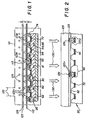
FIG. 1 shows schematically in partial cross-sectional view an
arrangement for depositing a color forming organic EL layer into designated
recessed surface portions of subpixels of a TFT array substrate by an aperture
mask method in accordance with the present invention;
FIG. 2 depicts schematically a side view of an arrangement for
depositing a color forming organic EL layer into designated recessed surface
portions of subpixels of a TFT array substrate by a optical mask method in
accordance with the present invention;
FIG. 3 is a schematic plan view of an aperture mask which is used
advantageously in the method of forming organic EL layers by the arrangement
shown in FIG. 1;
FIG. 4 shows a schematic side view of another optical mask method
useful for depositing a color forming organic EL layer into designated subpixels of
a TFT substrate in accordance with the present invention;
FIG. 5 illustrates in a schematic side view another optical mask
method of depositing a color forming organic EL layer into designated subpixels of
a TFT substrate in accordance with the present invention; and
FIG. 6 depicts a schematic side view of still another optical mask
method of depositing a color forming organic EL layer into designated subpixels of
a TFT substrate in accordance with the present invention.
It will be understood that the drawings are not to scale and have
been shown for clarity of illustration.
DETAILED DESCRIPTION OF THE INVENTION
The Arm "display" or "display panel" is employed to designate a
screen capable of electronically displaying video images or text. The term "pixel"
is employed in its art recognized usage to designate an area of a display panel that
can be stimulated to emit light independently of other areas. The term "multicolor"
is employed to describe a display panel that is capable of emitting light of a
different hue in different areas. In particular, it is employed to describe a display
panel that is capable of displaying images of different colors. These areas are not
necessarily contiguous. The term "full-color" is employed to describe multicolor
display panels that are capable of emitting in the red, green, and blue regions of the
visible spectrum and displaying images in any combination of hues. The red, green,
and blue colors constitute the three primary colors from which all other colors can
be generated by appropriately mixing these three primaries. The term "hue" refers
to the intensity profile of light emission within the visible spectrum, with different
hues exhibiting visually discernible differences in color. The pixel or subpixel is
generally used to designate the smallest addressable unit in a display panel. For a
monochrome display, there is no distinction between pixel or subpixels. The term
"subpixel" is used in multicolor display panel and is employed to designate any
portion of a pixel which can be independently addressable to emit a specific color.
For example, a blue subpixel is that portion of a pixel which can be addressed to
emit blue light. In a full-color display, a pixel generally comprises of three primary
color subpixels, namely, blue, green, and red. The term "pitch" is used to
designate the distance separating two pixels or subpixels in a display panel. Thus, a
subpixel pitch means the separation between two subpixels.
Turning now to FIG. 1, there is shown one preferred arrangement
for the practice of the method in accordance with the present invention. Arranged
within a reduced pressure chamber 121 having a pump port 122 is a TFT active
matrix array substrate 20 depicted schematically in cross-sectional view as
representing, for example, the major raised and recessed surface portions of a TFT
pixel shown in FIG. 9 of the above cited US-A-5,550,066.
Briefly described, such a pixel is comprised of an insulating
transparent substrate 41 and a plurality of layers deposited thereon. Among these
layers are two TFTs 44 and 48, an insulating layer 52, an upper electrode 62, a
transparent anode bottom electrode 72, and a passivating layer 74. This multilayer
construction of each pixel or subpixel of the TFT active matrix array substrate 20
results in raised surface portions 92 of each subpixel (only one most highly raised
portion is depicted in the drawings to provide clarity of presentation) and a
recessed surface portion 94 which reveals the bottom electrode 72.
An aperture mask 112 is positioned on, or in close proximity to, the
raised surface portions 92 of the pixels or subpixels 90 on the TFT substrate 20 in
an oriented relationship between the apertures 113 and the designated recessed
surface portions 94 of the substrate 20. The oriented relationship between the
apertures 113 of the aperture mask 112 and the designated recessed surface
portions 94 can he more readily visualized in conjunction with FIG. 3, where
orientation marks 152 (also referred to as alignment targets) are shown which are
used to orient the aperture mask 112 with respect to matching orientation marks
(not shown) on the TFT substrate 20. For example, the aperture mask 112 is
oriented with respect to the TFT substrate such that the apertures 113 are
positioned in a first-color (for example, a red organic EL medium) mask position
over the designated color subpixel portions 94 on the substrate. In a two-dimensional
array of TFT subpixels, the subpixels 90 are arranged in rows and
orthogonal columns, and the 113 on the aperture mask 112 are similarly arranged
in rows and columns, as indicated by the coordinates x and y in FIG. 3, whereby a
subpixel pitch in both the x and y directions indicates the distance between
subpixels. Depending upon the particular design and layout of the two-dimensional
TFT array, a ratio between a subpixel pitch in one direction and in an orthogonal
second direction can have a value ranging from 1 to 3.
Still referring to FIG. 3 in conjunction with FIG. 1, the aperture
mask 112 is repositioned on the rased surface portions 92 of the TFT active matrix
array substrate 20 in an oriented relationship between the apertures 113 and
corresponding designated recessed surface portions 94 such that in a second-color
(for example, a green organic EL medium) mask position a second-color (e.g.,
green) organic EL layer can be deposited into designated recessed electrodes of the
green subpixels. Similarly, repositioning the apes 113 into a third-color (for
example, a blue organic EL medium) mask position permits deposition of a third-color
(e.g., blue) organic EL layer into designated blue recessed surface portions of
the TFT array subpixels. In FIG. 3 the plurality of apertures 113 are depicted in a
solid outline corresponding to a first-color (e.g., red) mask position, in a dashed
outline corresponding to a second-color (e.g., green) mask position, and in a
dotted outline corresponding to a third-color (e.g., blue) mask position over the
corresponding recessed surface portions of the subpixels 90 in accordance with a
selected desired color pattern to be achieved in the full-color EL display array,
shown here for illustrative purposes as a diagonal color pattern.
Referring now again to FIG. 1, a donor support 124 having a
coating 123 on a surface facing the aperture mask 112, is spaced from the aperture
mask by a distance D, which is intended to indicate a distance which ensures a
position of a transferable relationship between the coating 123 on the support 124
and the aperture mask 112 with the plurality of apertures 113. The coating 123 is
designated as donor coating containing an organic EL medium of a specific color.
A plurality of heating elements 125 is arranged to heat the donor
support 124 in a reduced pressure environment to a temperature at which the EL
organic material of the donor coating 123 vaporizes as schematically indicated by
the dotted vapor arrows 123v, thereby forming a deposited electroluminescent
organic layer 123d over the aperture mask 112 and in the designated recessed
surface portion 94 of the TFT substrate subpixels 90 through the respective
plurality of apertures 113 of the aperture mask 112.
The donor support 124 with donor coating 123 thereupon enters
and leaves the chamber 121 through suitably designed ports (not shown). The
aperture mask 112 is repositioned with resect to the substrate and translated from
a first-color mask position to a second- or third-color mask position through a
precise mechanical position aligner (not shown).
The aperture mask is held in contact or close proximity to the
substrate, where close proximity is a spacing of less than 250 micrometers between
the aperture mask and the raised surface portions 92 of the subpixels.
Prior to actuating the heating elements 125, the chamber 121 is
preferably provided with an environment of reduced pressure. In the practice of the
present invention, the environment of reduced pressure is preferably at a pressure
value of less than 1 Torr during the heating step so that the organic material
transferred from the donor support forms a uniform layer in the designated
recessed surface portions 94 of the subpixels 90 of the TFT substrate 20.
In practice, the donor support 124 is first prepared by providing a
transferable coating of an organic EL donor medium thereon by a suitable process
forming the donor coating 123. Examples of suitable methods for coating the
support include solution coating, meniscus coating, dip coating, spraying, screen
printing, and vapor deposition coating in a vacuum chamber. These methods are
specifically designed to produce a uniform coating of precise thickness on a donor
support which may be a sheet, a rigid support such as glass, a foil, or a flexible
web. Using any of these methods, a support coated with a predetermined thickness
of the desired transferable EL organic donor medium can be readily prepared in
large quantity. A preferred method for the preparation of a flexible donor support,
such as for example, a donor web, is the roll-to-roll vacuum coating because the
coating thickness and uniformity on the support can be precisely controlled with an
accuracy of better than a few percent.
The donor support 124 can be made of any of several materials
which meet at least the following requirements. The donor support must be
capable of maintaining the structural integrity during the heat-induced transfer step.
Additionally, the donor support must be capable of receiving on one surface a
relatively thin coating of EL organic donor medium, and of retaining this coating
without degradation during anticipated storage periods of the coated support
Support materials meeting these requirements include, for example, metal foils,
certain plastic foils with a high glass transition temperature such as Kapton®.
While selection of suitable support materials can rely on known engineering
approaches, it will be appreciated that certain aspects of a selected support material
merit further consideration when configured as a donor support useful in the
practice of the invention. For example, the support may require a multi-step
cleaning and surface preparation process prior to precoating with a transferable EL
organic medium. If the support material is a radiation transmissive material, the
incorporation of a radiation-absorptive material on the donor support 124 may be
advantageous in enhancing the heat absorption and thus the transfer of donor
coating 123 from the donor support 124 to the recessed surface portions 94 of the
TFT substrate 20.
The transfer of the EL organic donor medium 123 from the donor
support 124 into the recessed surface portions 94 of the TFT substrate 20 can also
be caused by translating or scanning a heat source or a light source in proximity to
and along the support surface to be heated. While a scanning heat source may
increase the total time to form a layer in the designated recessed surface portions
94 of the subpixels 90, a scanning heat source may advantageously reduce
excessive heating of the substrate surface and any attendant undesirable
crystallization or aggregation of the layer 123d being formed in the subpixel
recesses of the substrate.
The aperture mask 112 is conveniently fabricated from a metallic
foil or sheet by micromachining methods well known in this art. Such
micromachining methods are capable of rendering the plurality of apertures 113
which can be as small as a few micrometers in dimension and, if the aperture mask
112 is to contain a plurality of closely spaced apertures, the distance between
adjacent apertures can also be as small as a few micrometers.
The orientation marks 152 (see FIG. 3) of the aperture mask 112
can be apertures through which a directed beam of a light can pass, or they can be
opaque in appearance. In any event, the orientation marks 152 on the aperture
mask 112 are used to position the aperture mask in an oriented relationship with
the TFT substrate 20 which has spatially matching or coincident sets of orientation
marks (not shown). Aperture masks defining a particular selected color pattern of
apertures are advantageously used in the practice of the invention to form full-color
organic EL layers in designated recessed surface portions of pixels in
correspondence with the selected particular color pattern.
The organic EL media used in the method of forming organic layers
in accordance with this invention can take any of the forms, such as those disclosed
in the following commonly assigned Tang US-A-4,356,429; VanSlyke et al US-A-4,539,507;
VanSlyke et al US-A-4,720,432; Tang et al US-A-4,885,211; Tang et
al US-A-4,769,292; Littman et al US-A-5,059,861; VanSlyke US-A-5,047,687;
VanSlyke et al US-A-5,059,862; VanSlyke et al US-A-5,061,617; and Tang et al
US-A-5,294,870; the disclosures of which are here incorporated by reference.
As disclosed in Tang et al US-A-5,294,870, cited above, a plurality
of organic layers which, together, are referred to as an EL medium, are known to
produce efficient organic electroluminescent devices. For example, an efficient EL
layer is formed on the bottom electrodes 72 by sequentially depositing a hole
injecting layer, a hole transporting layer, a luminescent layer, and an electron
injecting layer.
Numerous organic materials, disclosed in the above-cited
references, can be useful to form these organic EL layers on the recessed surface
portions of the substrate in accordance with the present invention. Selection of
particular organic EL media is influenced, among other considerations, by their
ability to provide uniform transferable donor coatings on a donor support, and by
their ability to maintain transferable properties during a storage interval between
preparation of a coating on the donor support and its deployment in the heat
transfer step.
With respect to the patterned organic layers in a full-color organic
EL display on the TFT substrate, the light emitting properties of each of the layers
are tailored to provide light emission over specific spectral regions of the visible
spectrum by incorporating into the donor coating 123 and thereby into the
deposited layers 123d a combination of an electroluminescent organic host material
and at least one highly fluorescent organic material. A different transferable
organic EL coating is precoated on a donor support for each of the primary colors
(red, green, and blue) to be obtained in a full-color organic EL display. For
example, if the designated red subpixels are to provide light emission in a red
spectral region of the visible spectrum, the organic EL host material is combined
with a highly fluorescent organic dye tailored to emit red light when such a red
light emitting subpixel of a multicolor organic EL display is actuated by at least one
of the TFTs 44, 48 corresponding to that particular subpixel. Likewise, if a second
selected color of emitted light is to be emitted within a green spectral region, a
donor coating 123 is prepared by suitably combining an organic EL host material
with a green light emitting highly fluorescent dye. Similarly, if designated recessed
surface portions 94 of subpixels 90 are to receive a blue light emitting EL medium,
a donor coating consisting of a combination of a organic EL material and a blue
light emitting highly fluorescent dye is prepared on the donor support. The hole
injecting layer, the hole transport layer, and the electron transport layer, which
together perform the charge transport functions, do not require patterning, and
therefore can be deposited by a conventional vapor deposition method.
Referring now to FIG. 2, there is shown a simplified rendition of a
TFT active matrix array substrate 20 identical to the substrate described with
reference to FIG. 1. Like numeral designations denote like parts or functions. The
method of forming patterned organic layers in a full-color EL display on the two-dimensional
TFT substrate is distinct over the method previously described with
reference to FIG. 1, in that the transferable coating 123 of a color forming EL
donor material is precoated on one surface of an optical mask which is comprised
of a pattern of absorbers 126. The patterned absorbers are formed on a heat
transmissive or on a light transmissive optical mask support 129, through which
radiation (heat, light) 130 is incident. The incident radiation 130 is preferentially
absorbed by the patterned heat absorbers 126, thereby causing the EL medium in
coating 123 to be selectively heated and thus transferred as a vapor 123v from the
optical mask to the bottom electrodes 72 of the designated color EL subpixels and
thus depositing the red, green, or blue color EL subpixels designated at 123d.
When the incident radiation 130 is from a heat source, the patterned
absorbers 126 function as heat absorbers. When the incident radiation 130 is from
a light source, the patterned absorbers 126 are light absorbers.
The transferable coating 123 on the optical mask is held in contact
or close proximity to the substrate during the vapor deposition transfer step. Close
proximity is a spacing of less than 250 micrometers between the coating 123 and
the raised surface portions 92 of the subpixels.
The method of FIG. 2 of forming a full-color organic EL display on
a TFT substrate is preferably practiced in an environment of reduced pressure
during the pattern-selective transfer and deposition of the EL medium for each of
the color EL subpixels. For simplicity of presentation, the reduced pressure
chamber 121 of FIG. 1 is not shown in FIG. 2.
The optical mask support 129 can be of any material which is
transmissive to the incident radiation 130 and which provides structural integrity
under the conditions of use of the optical mask. Glass, quartz, and sapphire are
examples of suitable optical mask support materials.
The pattern of absorbers 126 can, in principle, be made from any
material which is capable of preferentially absorbing radiation (heat or light) with
respect to the mask support 123. In practicing the method of the invention, at least
the following considerations influence the selection of preferred absorber materials:
the optical mask should be reusable and, accordingly, should be readily cleanable
prior to recoating with a transferable coating of a color forming EL donor material;
the patterned absorbers should be highly adherent to the aforementioned mask
support materials, and remain highly adherent under the conditions of exposure to
high temperature during repeated use of the optical mask.
In view of the above considerations, examples of preferred materials
for forming the pattern of absorbers include patterns of carbon, thin metal layer
such as chromium, metal/semiconductor alloyed layers such as
chromium/germanium multilayers, and a material known in the art as "black
chrome."
The incident radiation, depicted by arrows 130, can be from a
pulsed light where the pulse width can range from tens of milliseconds to
nanoseconds. Alternatively, focused scanning light sources can be used
advantageously in the practice of the methods, including laser sources. In using a
seaming source, the light source is focused onto a small area (e.g., 1 mm x 1 mm)
and is swept across the surface of the optical mask. In the scan mode, the light
source can either be continuous or pulsed.
Referring now to FIG. 4, there is shown a schematic side view of
another optical mask method useful for depositing a color forming EL layer into
designated subpixels of a TFT substrate The optical mask of FIG. 4 is distinct over
the optical mask of FIG. 2 in that a heat insulating layer 128 is shown as uniformly
covering the surface adjacent to the substrate 20 of a radiation transmissive optical
mask support 129. On the surface of the heat insulating layer 128 are disposed
absorbers 126 which constitute a subpixel pattern for one of the color forming EL
media. A transferable coating 123 of a color forming EL donor material is provided
over the heat insulating layer 128 and over the patterned absorbers 126.
The transferable coating 123 on the optical mask is held in contact
or close proximity to the substrate during the vapor deposition transfer step, as
described above with reference to FIG. 2.
The heat insulating layer minimizes heat loss to the optical mask
support 129 from the heat absorbers 126, thereby enhancing vapor deposition of
the EL layers via vapor paths 123v at a given level of incident radiation (heat or
light radiation) as indicated by the arrows 130.
Examples of suitable heat insulating layers 128 include high
temperature polymers, for example, polycarbonate, polyimide, and
photocrosslinkable resins, low density silica gels, and, in general, any nonabsorbing
material of a lower thermal capacity than that of the mask support 129. The heat
insulating layer is subject to the same aforementioned considerations of physical
integrity as are the optical mask support 129 and the absorbers 126.
Referring now to FIG. 5, there is depicted a schematic side view of
another optical mask method useful for vapor depositing a color forming organic
EL layer into designated subpixels of a TFT substrate. In contrast to the optical
mask described with reference to FIG. 2, the optical mask of FIG. 5 has, on the
surface of the mask support 129 adjacent to the TFT substrate 20, not only a
pattern of absorbers 126, but reflectors 127 disposed on that surface. The
reflectors 127 cover the area of the mask support surface between the absorbers
126.
A donor coating 123 of a color forming organic EL medium is
formed over the absorbers 126 and over the reflectors 127.
The transferable coating 123 on the optical mask is held in contact
or close proximity to the substrate during the vapor deposition transfer step, as
described above with reference to FIG. 2.
The reflectors 127 reflect the radiation 130 incident thereon through
the radiation transmissive mask support 129, thereby minimizing a temperature
increase of the donor EL coating 123 in all coating regions except for the regions
defined by the pattern of absorbers 126.
The reflectors 127 are preferably made from a thin film of a
reflective metal such as, for example, a thin film of reflective chromium, referred to
in the art also as "bright chrome," which is known to be highly adherent to the
aforementioned optical mask support materials, and to be abrasion resistant.
Although not shown in FIG. 5 for clarity of presentation, the optical
mask method of forming a full-color organic EL display depicted in FIG. 5 is
preferably practiced in an environment of reduced pressure during the deposition of
the EL medium for each of the color EL subpixels.
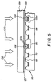
Referring now to FIG. 6, there is shown another optical mask
method of vapor depositing a color forming organic EL layer into designated
subpixels of a TFT substrate. Here, the optical mask has, on a surface adjacent to
the TFT substrate 20 of the radiation transmissive mask support 129, in sequence,
a heat insulating layer 128, a pattern of absorbers 126 with reflectors 127
therebetween, and a donor coating 123 of a color forming organic EL medium.
Thus, the method of FIG. 6 combines the features and functions previously
described with reference to the optical mask vapor deposition method of FIG. 2,
FIG. 4, and FIG. 5.
While one particular configuration and fabrication of a TFT array,
and the deposition thereon of a single-color organic EL layer has been described in
commonly assigned US-A-5,550,066 to Tang et al, the present invention
contemplates that providing a TFT substrate includes selecting a polysilicon TFT
array on a quartz substrate, a polysilicon TFT array on a glass substrate, an
amorphous silicon TFT array on a glass substrate, or a TFT array on a crystalline
silicon substrate.
Furthermore, it is desirable in certain applications of a full-color
organic EL display formed on a TFT substrate to provide the EL emitted light
through the top electrode 84. Accordingly, the present invention anticipates
providing an organic EL display array on a TFT substrate in which the top
electrode 84 is a transparent conductor. Alternatively, for other applications, it is
desirable to furnish the bottom electrode 72 as the transparent conductor in a TFT
substrate.
PARTS LIST
- 20
- thin film transistor active matrix array substrate
- 41
- insulating transparent substrate
- 44
- thin film transistors (two per pixel)
- 48
- thin film transistors (two per pixel)
- 52
- insulating layer
- 62
- upper electrode
- 72
- bottom electrode
- 74
- passivating layer
- 84
- top electrode
- 90
- subpixel
- 92
- raised surface portions of a subpixel
- 94
- recessed surface portion of a subpixel
- 112
- aperture mask
- 113
- plurality of apertues
- 121
- reduced pressure chamber
- 122
- pump port
- 123
- coating of organic EL donor material
- 123d
- deposited EL donor layer
- 123v
- donor vapor
- 124
- donor support
- 125
- heating elements
- 126
- absorbers
- 127
- reflectors
- 128
- heat insulating layer
- 129
- optical mask support
- 130
- incident radiation
- 152
- orientation marks