EP0860885A2 - Photovoltaic device, photoelectric transducer and method of manufacturing same - Google Patents
Photovoltaic device, photoelectric transducer and method of manufacturing same Download PDFInfo
- Publication number
- EP0860885A2 EP0860885A2 EP98102791A EP98102791A EP0860885A2 EP 0860885 A2 EP0860885 A2 EP 0860885A2 EP 98102791 A EP98102791 A EP 98102791A EP 98102791 A EP98102791 A EP 98102791A EP 0860885 A2 EP0860885 A2 EP 0860885A2
- Authority
- EP
- European Patent Office
- Prior art keywords
- semiconductor layer
- type semiconductor
- grain size
- average grain
- photovoltaic device
- Prior art date
- Legal status (The legal status is an assumption and is not a legal conclusion. Google has not performed a legal analysis and makes no representation as to the accuracy of the status listed.)
- Granted
Links
- 238000004519 manufacturing process Methods 0.000 title claims abstract description 25
- 239000004065 semiconductor Substances 0.000 claims abstract description 285
- 239000013078 crystal Substances 0.000 claims abstract description 56
- 238000009826 distribution Methods 0.000 claims abstract description 29
- 229910052739 hydrogen Inorganic materials 0.000 claims description 25
- 239000001257 hydrogen Substances 0.000 claims description 24
- UFHFLCQGNIYNRP-UHFFFAOYSA-N Hydrogen Chemical compound [H][H] UFHFLCQGNIYNRP-UHFFFAOYSA-N 0.000 claims description 23
- 238000005268 plasma chemical vapour deposition Methods 0.000 claims description 17
- 229910021421 monocrystalline silicon Inorganic materials 0.000 claims description 14
- 239000002019 doping agent Substances 0.000 claims description 9
- 230000015572 biosynthetic process Effects 0.000 claims description 3
- 238000000034 method Methods 0.000 abstract description 23
- 238000006243 chemical reaction Methods 0.000 abstract description 14
- 230000003287 optical effect Effects 0.000 abstract description 9
- 239000010410 layer Substances 0.000 description 231
- 229910021424 microcrystalline silicon Inorganic materials 0.000 description 53
- 239000010408 film Substances 0.000 description 45
- 238000002474 experimental method Methods 0.000 description 40
- 229910021417 amorphous silicon Inorganic materials 0.000 description 26
- 230000000694 effects Effects 0.000 description 26
- 239000000758 substrate Substances 0.000 description 26
- 238000000151 deposition Methods 0.000 description 16
- 230000008021 deposition Effects 0.000 description 14
- 239000007789 gas Substances 0.000 description 14
- 239000000969 carrier Substances 0.000 description 13
- 239000000463 material Substances 0.000 description 13
- 230000001276 controlling effect Effects 0.000 description 11
- 238000009792 diffusion process Methods 0.000 description 10
- 229910052751 metal Inorganic materials 0.000 description 10
- 239000002184 metal Substances 0.000 description 10
- 239000010409 thin film Substances 0.000 description 9
- 230000002829 reductive effect Effects 0.000 description 8
- OAICVXFJPJFONN-UHFFFAOYSA-N Phosphorus Chemical compound [P] OAICVXFJPJFONN-UHFFFAOYSA-N 0.000 description 7
- 238000001069 Raman spectroscopy Methods 0.000 description 7
- 238000002425 crystallisation Methods 0.000 description 7
- 230000008025 crystallization Effects 0.000 description 7
- 230000008859 change Effects 0.000 description 6
- 229910010271 silicon carbide Inorganic materials 0.000 description 6
- XOLBLPGZBRYERU-UHFFFAOYSA-N tin dioxide Chemical compound O=[Sn]=O XOLBLPGZBRYERU-UHFFFAOYSA-N 0.000 description 6
- BLRPTPMANUNPDV-UHFFFAOYSA-N Silane Chemical compound [SiH4] BLRPTPMANUNPDV-UHFFFAOYSA-N 0.000 description 5
- 238000002441 X-ray diffraction Methods 0.000 description 5
- 239000003795 chemical substances by application Substances 0.000 description 5
- 229910052731 fluorine Inorganic materials 0.000 description 5
- 230000031700 light absorption Effects 0.000 description 5
- 239000000203 mixture Substances 0.000 description 5
- 229910003465 moissanite Inorganic materials 0.000 description 5
- 230000006798 recombination Effects 0.000 description 5
- 238000005215 recombination Methods 0.000 description 5
- 238000004544 sputter deposition Methods 0.000 description 5
- 229910001220 stainless steel Inorganic materials 0.000 description 5
- 239000010935 stainless steel Substances 0.000 description 5
- 239000000126 substance Substances 0.000 description 5
- 238000010521 absorption reaction Methods 0.000 description 4
- 229910045601 alloy Inorganic materials 0.000 description 4
- 239000000956 alloy Substances 0.000 description 4
- 229910052782 aluminium Inorganic materials 0.000 description 4
- 125000004122 cyclic group Chemical group 0.000 description 4
- 238000011156 evaluation Methods 0.000 description 4
- 229910021420 polycrystalline silicon Inorganic materials 0.000 description 4
- KFZMGEQAYNKOFK-UHFFFAOYSA-N Isopropanol Chemical compound CC(C)O KFZMGEQAYNKOFK-UHFFFAOYSA-N 0.000 description 3
- 229910000577 Silicon-germanium Inorganic materials 0.000 description 3
- 229910052796 boron Inorganic materials 0.000 description 3
- 239000010931 gold Substances 0.000 description 3
- 230000006872 improvement Effects 0.000 description 3
- PJXISJQVUVHSOJ-UHFFFAOYSA-N indium(III) oxide Inorganic materials [O-2].[O-2].[O-2].[In+3].[In+3] PJXISJQVUVHSOJ-UHFFFAOYSA-N 0.000 description 3
- 239000011810 insulating material Substances 0.000 description 3
- 239000013081 microcrystal Substances 0.000 description 3
- 238000005498 polishing Methods 0.000 description 3
- 230000008569 process Effects 0.000 description 3
- 229910052710 silicon Inorganic materials 0.000 description 3
- 239000011135 tin Substances 0.000 description 3
- 238000007740 vapor deposition Methods 0.000 description 3
- CSCPPACGZOOCGX-UHFFFAOYSA-N Acetone Chemical compound CC(C)=O CSCPPACGZOOCGX-UHFFFAOYSA-N 0.000 description 2
- IJGRMHOSHXDMSA-UHFFFAOYSA-N Atomic nitrogen Chemical compound N#N IJGRMHOSHXDMSA-UHFFFAOYSA-N 0.000 description 2
- ZOXJGFHDIHLPTG-UHFFFAOYSA-N Boron Chemical compound [B] ZOXJGFHDIHLPTG-UHFFFAOYSA-N 0.000 description 2
- RYGMFSIKBFXOCR-UHFFFAOYSA-N Copper Chemical compound [Cu] RYGMFSIKBFXOCR-UHFFFAOYSA-N 0.000 description 2
- YCKRFDGAMUMZLT-UHFFFAOYSA-N Fluorine atom Chemical compound [F] YCKRFDGAMUMZLT-UHFFFAOYSA-N 0.000 description 2
- XEEYBQQBJWHFJM-UHFFFAOYSA-N Iron Chemical compound [Fe] XEEYBQQBJWHFJM-UHFFFAOYSA-N 0.000 description 2
- PXHVJJICTQNCMI-UHFFFAOYSA-N Nickel Chemical compound [Ni] PXHVJJICTQNCMI-UHFFFAOYSA-N 0.000 description 2
- BQCADISMDOOEFD-UHFFFAOYSA-N Silver Chemical compound [Ag] BQCADISMDOOEFD-UHFFFAOYSA-N 0.000 description 2
- 229910000831 Steel Inorganic materials 0.000 description 2
- GWEVSGVZZGPLCZ-UHFFFAOYSA-N Titan oxide Chemical compound O=[Ti]=O GWEVSGVZZGPLCZ-UHFFFAOYSA-N 0.000 description 2
- 238000000862 absorption spectrum Methods 0.000 description 2
- XAGFODPZIPBFFR-UHFFFAOYSA-N aluminium Chemical compound [Al] XAGFODPZIPBFFR-UHFFFAOYSA-N 0.000 description 2
- 229910052787 antimony Inorganic materials 0.000 description 2
- WMWLMWRWZQELOS-UHFFFAOYSA-N bismuth(iii) oxide Chemical compound O=[Bi]O[Bi]=O WMWLMWRWZQELOS-UHFFFAOYSA-N 0.000 description 2
- 229910052799 carbon Inorganic materials 0.000 description 2
- 230000015556 catabolic process Effects 0.000 description 2
- 229910010293 ceramic material Inorganic materials 0.000 description 2
- 229910052804 chromium Inorganic materials 0.000 description 2
- 239000011651 chromium Substances 0.000 description 2
- 150000001875 compounds Chemical class 0.000 description 2
- 239000004020 conductor Substances 0.000 description 2
- 229910052802 copper Inorganic materials 0.000 description 2
- 239000010949 copper Substances 0.000 description 2
- 238000006731 degradation reaction Methods 0.000 description 2
- 238000010790 dilution Methods 0.000 description 2
- 239000012895 dilution Substances 0.000 description 2
- 239000011737 fluorine Substances 0.000 description 2
- 239000011521 glass Substances 0.000 description 2
- PCHJSUWPFVWCPO-UHFFFAOYSA-N gold Chemical compound [Au] PCHJSUWPFVWCPO-UHFFFAOYSA-N 0.000 description 2
- 229910052737 gold Inorganic materials 0.000 description 2
- 229910052738 indium Inorganic materials 0.000 description 2
- AMGQUBHHOARCQH-UHFFFAOYSA-N indium;oxotin Chemical compound [In].[Sn]=O AMGQUBHHOARCQH-UHFFFAOYSA-N 0.000 description 2
- 229910052745 lead Inorganic materials 0.000 description 2
- 239000011133 lead Substances 0.000 description 2
- 238000001755 magnetron sputter deposition Methods 0.000 description 2
- JKQOBWVOAYFWKG-UHFFFAOYSA-N molybdenum trioxide Chemical compound O=[Mo](=O)=O JKQOBWVOAYFWKG-UHFFFAOYSA-N 0.000 description 2
- 229910052758 niobium Inorganic materials 0.000 description 2
- 239000010955 niobium Substances 0.000 description 2
- 238000007747 plating Methods 0.000 description 2
- -1 polyethylene Polymers 0.000 description 2
- 230000002035 prolonged effect Effects 0.000 description 2
- 239000011241 protective layer Substances 0.000 description 2
- 230000009467 reduction Effects 0.000 description 2
- 229910052709 silver Inorganic materials 0.000 description 2
- 239000004332 silver Substances 0.000 description 2
- 239000007921 spray Substances 0.000 description 2
- 239000010959 steel Substances 0.000 description 2
- 229910052715 tantalum Inorganic materials 0.000 description 2
- 229910052718 tin Inorganic materials 0.000 description 2
- 229910052719 titanium Inorganic materials 0.000 description 2
- 239000010936 titanium Substances 0.000 description 2
- 238000002834 transmittance Methods 0.000 description 2
- 229910000789 Aluminium-silicon alloy Inorganic materials 0.000 description 1
- OKTJSMMVPCPJKN-UHFFFAOYSA-N Carbon Chemical compound [C] OKTJSMMVPCPJKN-UHFFFAOYSA-N 0.000 description 1
- VYZAMTAEIAYCRO-UHFFFAOYSA-N Chromium Chemical compound [Cr] VYZAMTAEIAYCRO-UHFFFAOYSA-N 0.000 description 1
- ZOKXTWBITQBERF-UHFFFAOYSA-N Molybdenum Chemical compound [Mo] ZOKXTWBITQBERF-UHFFFAOYSA-N 0.000 description 1
- 239000004952 Polyamide Substances 0.000 description 1
- 239000004698 Polyethylene Substances 0.000 description 1
- 239000004642 Polyimide Substances 0.000 description 1
- 239000004743 Polypropylene Substances 0.000 description 1
- 239000004793 Polystyrene Substances 0.000 description 1
- 229920001328 Polyvinylidene chloride Polymers 0.000 description 1
- 229910020328 SiSn Inorganic materials 0.000 description 1
- XUIMIQQOPSSXEZ-UHFFFAOYSA-N Silicon Chemical compound [Si] XUIMIQQOPSSXEZ-UHFFFAOYSA-N 0.000 description 1
- RTAQQCXQSZGOHL-UHFFFAOYSA-N Titanium Chemical compound [Ti] RTAQQCXQSZGOHL-UHFFFAOYSA-N 0.000 description 1
- QCWXUUIWCKQGHC-UHFFFAOYSA-N Zirconium Chemical compound [Zr] QCWXUUIWCKQGHC-UHFFFAOYSA-N 0.000 description 1
- 229910017875 a-SiN Inorganic materials 0.000 description 1
- 230000002159 abnormal effect Effects 0.000 description 1
- 239000002253 acid Substances 0.000 description 1
- 230000004913 activation Effects 0.000 description 1
- 230000002411 adverse Effects 0.000 description 1
- PNEYBMLMFCGWSK-UHFFFAOYSA-N aluminium oxide Inorganic materials [O-2].[O-2].[O-2].[Al+3].[Al+3] PNEYBMLMFCGWSK-UHFFFAOYSA-N 0.000 description 1
- 239000007864 aqueous solution Substances 0.000 description 1
- 229910052785 arsenic Inorganic materials 0.000 description 1
- 125000004429 atom Chemical group 0.000 description 1
- QVGXLLKOCUKJST-UHFFFAOYSA-N atomic oxygen Chemical compound [O] QVGXLLKOCUKJST-UHFFFAOYSA-N 0.000 description 1
- 230000004888 barrier function Effects 0.000 description 1
- 230000008901 benefit Effects 0.000 description 1
- 229910052794 bromium Inorganic materials 0.000 description 1
- CXKCTMHTOKXKQT-UHFFFAOYSA-N cadmium oxide Inorganic materials [Cd]=O CXKCTMHTOKXKQT-UHFFFAOYSA-N 0.000 description 1
- 229920002301 cellulose acetate Polymers 0.000 description 1
- 229910052801 chlorine Inorganic materials 0.000 description 1
- VNNRSPGTAMTISX-UHFFFAOYSA-N chromium nickel Chemical compound [Cr].[Ni] VNNRSPGTAMTISX-UHFFFAOYSA-N 0.000 description 1
- 239000010941 cobalt Substances 0.000 description 1
- 229910017052 cobalt Inorganic materials 0.000 description 1
- GUTLYIVDDKVIGB-UHFFFAOYSA-N cobalt atom Chemical compound [Co] GUTLYIVDDKVIGB-UHFFFAOYSA-N 0.000 description 1
- 230000008094 contradictory effect Effects 0.000 description 1
- 229910021419 crystalline silicon Inorganic materials 0.000 description 1
- 230000003247 decreasing effect Effects 0.000 description 1
- 230000007547 defect Effects 0.000 description 1
- SWXVUIWOUIDPGS-UHFFFAOYSA-N diacetone alcohol Natural products CC(=O)CC(C)(C)O SWXVUIWOUIDPGS-UHFFFAOYSA-N 0.000 description 1
- 229910003460 diamond Inorganic materials 0.000 description 1
- 239000010432 diamond Substances 0.000 description 1
- 238000007598 dipping method Methods 0.000 description 1
- 239000012789 electroconductive film Substances 0.000 description 1
- 238000010894 electron beam technology Methods 0.000 description 1
- 238000005530 etching Methods 0.000 description 1
- 229910052733 gallium Inorganic materials 0.000 description 1
- 229910052732 germanium Inorganic materials 0.000 description 1
- 150000002431 hydrogen Chemical class 0.000 description 1
- 238000007654 immersion Methods 0.000 description 1
- 239000012535 impurity Substances 0.000 description 1
- 230000005764 inhibitory process Effects 0.000 description 1
- 229910052740 iodine Inorganic materials 0.000 description 1
- 229910052742 iron Inorganic materials 0.000 description 1
- 230000001788 irregular Effects 0.000 description 1
- 229960004592 isopropanol Drugs 0.000 description 1
- 150000002739 metals Chemical class 0.000 description 1
- 229910052750 molybdenum Inorganic materials 0.000 description 1
- 239000011733 molybdenum Substances 0.000 description 1
- 229910001120 nichrome Inorganic materials 0.000 description 1
- 229910052759 nickel Inorganic materials 0.000 description 1
- GUCVJGMIXFAOAE-UHFFFAOYSA-N niobium atom Chemical compound [Nb] GUCVJGMIXFAOAE-UHFFFAOYSA-N 0.000 description 1
- 229910052757 nitrogen Inorganic materials 0.000 description 1
- 229910052760 oxygen Inorganic materials 0.000 description 1
- 239000001301 oxygen Substances 0.000 description 1
- 239000002245 particle Substances 0.000 description 1
- 229910052698 phosphorus Inorganic materials 0.000 description 1
- 230000000704 physical effect Effects 0.000 description 1
- 229910052697 platinum Inorganic materials 0.000 description 1
- BASFCYQUMIYNBI-UHFFFAOYSA-N platinum Substances [Pt] BASFCYQUMIYNBI-UHFFFAOYSA-N 0.000 description 1
- 229920002647 polyamide Polymers 0.000 description 1
- 229920000515 polycarbonate Polymers 0.000 description 1
- 239000004417 polycarbonate Substances 0.000 description 1
- 229920000728 polyester Polymers 0.000 description 1
- 229920000573 polyethylene Polymers 0.000 description 1
- 229920001721 polyimide Polymers 0.000 description 1
- 229920001155 polypropylene Polymers 0.000 description 1
- 229920002223 polystyrene Polymers 0.000 description 1
- 229920000915 polyvinyl chloride Polymers 0.000 description 1
- 239000004800 polyvinyl chloride Substances 0.000 description 1
- 239000005033 polyvinylidene chloride Substances 0.000 description 1
- 238000002310 reflectometry Methods 0.000 description 1
- 230000001105 regulatory effect Effects 0.000 description 1
- 239000012779 reinforcing material Substances 0.000 description 1
- 239000011347 resin Substances 0.000 description 1
- 229920005989 resin Polymers 0.000 description 1
- 239000010703 silicon Substances 0.000 description 1
- 229910052814 silicon oxide Inorganic materials 0.000 description 1
- 239000002356 single layer Substances 0.000 description 1
- 229910000679 solder Inorganic materials 0.000 description 1
- 238000004381 surface treatment Methods 0.000 description 1
- 229920003002 synthetic resin Polymers 0.000 description 1
- 239000000057 synthetic resin Substances 0.000 description 1
- GUVRBAGPIYLISA-UHFFFAOYSA-N tantalum atom Chemical compound [Ta] GUVRBAGPIYLISA-UHFFFAOYSA-N 0.000 description 1
- 229910052716 thallium Inorganic materials 0.000 description 1
- 230000032258 transport Effects 0.000 description 1
- 229910052721 tungsten Inorganic materials 0.000 description 1
- WFKWXMTUELFFGS-UHFFFAOYSA-N tungsten Chemical compound [W] WFKWXMTUELFFGS-UHFFFAOYSA-N 0.000 description 1
- 239000010937 tungsten Substances 0.000 description 1
- 238000007738 vacuum evaporation Methods 0.000 description 1
- 229910052720 vanadium Inorganic materials 0.000 description 1
- 238000003079 width control Methods 0.000 description 1
- 229910052726 zirconium Inorganic materials 0.000 description 1
Images


Classifications
-
- H—ELECTRICITY
- H01—ELECTRIC ELEMENTS
- H01L—SEMICONDUCTOR DEVICES NOT COVERED BY CLASS H10
- H01L31/00—Semiconductor devices sensitive to infrared radiation, light, electromagnetic radiation of shorter wavelength or corpuscular radiation and specially adapted either for the conversion of the energy of such radiation into electrical energy or for the control of electrical energy by such radiation; Processes or apparatus specially adapted for the manufacture or treatment thereof or of parts thereof; Details thereof
- H01L31/0248—Semiconductor devices sensitive to infrared radiation, light, electromagnetic radiation of shorter wavelength or corpuscular radiation and specially adapted either for the conversion of the energy of such radiation into electrical energy or for the control of electrical energy by such radiation; Processes or apparatus specially adapted for the manufacture or treatment thereof or of parts thereof; Details thereof characterised by their semiconductor bodies
- H01L31/036—Semiconductor devices sensitive to infrared radiation, light, electromagnetic radiation of shorter wavelength or corpuscular radiation and specially adapted either for the conversion of the energy of such radiation into electrical energy or for the control of electrical energy by such radiation; Processes or apparatus specially adapted for the manufacture or treatment thereof or of parts thereof; Details thereof characterised by their semiconductor bodies characterised by their crystalline structure or particular orientation of the crystalline planes
- H01L31/0368—Semiconductor devices sensitive to infrared radiation, light, electromagnetic radiation of shorter wavelength or corpuscular radiation and specially adapted either for the conversion of the energy of such radiation into electrical energy or for the control of electrical energy by such radiation; Processes or apparatus specially adapted for the manufacture or treatment thereof or of parts thereof; Details thereof characterised by their semiconductor bodies characterised by their crystalline structure or particular orientation of the crystalline planes including polycrystalline semiconductors
- H01L31/03682—Semiconductor devices sensitive to infrared radiation, light, electromagnetic radiation of shorter wavelength or corpuscular radiation and specially adapted either for the conversion of the energy of such radiation into electrical energy or for the control of electrical energy by such radiation; Processes or apparatus specially adapted for the manufacture or treatment thereof or of parts thereof; Details thereof characterised by their semiconductor bodies characterised by their crystalline structure or particular orientation of the crystalline planes including polycrystalline semiconductors including only elements of Group IV of the Periodic System
- H01L31/03685—Semiconductor devices sensitive to infrared radiation, light, electromagnetic radiation of shorter wavelength or corpuscular radiation and specially adapted either for the conversion of the energy of such radiation into electrical energy or for the control of electrical energy by such radiation; Processes or apparatus specially adapted for the manufacture or treatment thereof or of parts thereof; Details thereof characterised by their semiconductor bodies characterised by their crystalline structure or particular orientation of the crystalline planes including polycrystalline semiconductors including only elements of Group IV of the Periodic System including microcrystalline silicon, uc-Si
-
- H—ELECTRICITY
- H01—ELECTRIC ELEMENTS
- H01L—SEMICONDUCTOR DEVICES NOT COVERED BY CLASS H10
- H01L31/00—Semiconductor devices sensitive to infrared radiation, light, electromagnetic radiation of shorter wavelength or corpuscular radiation and specially adapted either for the conversion of the energy of such radiation into electrical energy or for the control of electrical energy by such radiation; Processes or apparatus specially adapted for the manufacture or treatment thereof or of parts thereof; Details thereof
- H01L31/04—Semiconductor devices sensitive to infrared radiation, light, electromagnetic radiation of shorter wavelength or corpuscular radiation and specially adapted either for the conversion of the energy of such radiation into electrical energy or for the control of electrical energy by such radiation; Processes or apparatus specially adapted for the manufacture or treatment thereof or of parts thereof; Details thereof adapted as photovoltaic [PV] conversion devices
- H01L31/06—Semiconductor devices sensitive to infrared radiation, light, electromagnetic radiation of shorter wavelength or corpuscular radiation and specially adapted either for the conversion of the energy of such radiation into electrical energy or for the control of electrical energy by such radiation; Processes or apparatus specially adapted for the manufacture or treatment thereof or of parts thereof; Details thereof adapted as photovoltaic [PV] conversion devices characterised by at least one potential-jump barrier or surface barrier
- H01L31/075—Semiconductor devices sensitive to infrared radiation, light, electromagnetic radiation of shorter wavelength or corpuscular radiation and specially adapted either for the conversion of the energy of such radiation into electrical energy or for the control of electrical energy by such radiation; Processes or apparatus specially adapted for the manufacture or treatment thereof or of parts thereof; Details thereof adapted as photovoltaic [PV] conversion devices characterised by at least one potential-jump barrier or surface barrier the potential barriers being only of the PIN type
-
- H—ELECTRICITY
- H01—ELECTRIC ELEMENTS
- H01L—SEMICONDUCTOR DEVICES NOT COVERED BY CLASS H10
- H01L31/00—Semiconductor devices sensitive to infrared radiation, light, electromagnetic radiation of shorter wavelength or corpuscular radiation and specially adapted either for the conversion of the energy of such radiation into electrical energy or for the control of electrical energy by such radiation; Processes or apparatus specially adapted for the manufacture or treatment thereof or of parts thereof; Details thereof
- H01L31/18—Processes or apparatus specially adapted for the manufacture or treatment of these devices or of parts thereof
- H01L31/1804—Processes or apparatus specially adapted for the manufacture or treatment of these devices or of parts thereof comprising only elements of Group IV of the Periodic System
- H01L31/182—Special manufacturing methods for polycrystalline Si, e.g. Si ribbon, poly Si ingots, thin films of polycrystalline Si
- H01L31/1824—Special manufacturing methods for microcrystalline Si, uc-Si
-
- Y—GENERAL TAGGING OF NEW TECHNOLOGICAL DEVELOPMENTS; GENERAL TAGGING OF CROSS-SECTIONAL TECHNOLOGIES SPANNING OVER SEVERAL SECTIONS OF THE IPC; TECHNICAL SUBJECTS COVERED BY FORMER USPC CROSS-REFERENCE ART COLLECTIONS [XRACs] AND DIGESTS
- Y02—TECHNOLOGIES OR APPLICATIONS FOR MITIGATION OR ADAPTATION AGAINST CLIMATE CHANGE
- Y02E—REDUCTION OF GREENHOUSE GAS [GHG] EMISSIONS, RELATED TO ENERGY GENERATION, TRANSMISSION OR DISTRIBUTION
- Y02E10/00—Energy generation through renewable energy sources
- Y02E10/50—Photovoltaic [PV] energy
- Y02E10/545—Microcrystalline silicon PV cells
-
- Y—GENERAL TAGGING OF NEW TECHNOLOGICAL DEVELOPMENTS; GENERAL TAGGING OF CROSS-SECTIONAL TECHNOLOGIES SPANNING OVER SEVERAL SECTIONS OF THE IPC; TECHNICAL SUBJECTS COVERED BY FORMER USPC CROSS-REFERENCE ART COLLECTIONS [XRACs] AND DIGESTS
- Y02—TECHNOLOGIES OR APPLICATIONS FOR MITIGATION OR ADAPTATION AGAINST CLIMATE CHANGE
- Y02E—REDUCTION OF GREENHOUSE GAS [GHG] EMISSIONS, RELATED TO ENERGY GENERATION, TRANSMISSION OR DISTRIBUTION
- Y02E10/00—Energy generation through renewable energy sources
- Y02E10/50—Photovoltaic [PV] energy
- Y02E10/547—Monocrystalline silicon PV cells
-
- Y—GENERAL TAGGING OF NEW TECHNOLOGICAL DEVELOPMENTS; GENERAL TAGGING OF CROSS-SECTIONAL TECHNOLOGIES SPANNING OVER SEVERAL SECTIONS OF THE IPC; TECHNICAL SUBJECTS COVERED BY FORMER USPC CROSS-REFERENCE ART COLLECTIONS [XRACs] AND DIGESTS
- Y02—TECHNOLOGIES OR APPLICATIONS FOR MITIGATION OR ADAPTATION AGAINST CLIMATE CHANGE
- Y02E—REDUCTION OF GREENHOUSE GAS [GHG] EMISSIONS, RELATED TO ENERGY GENERATION, TRANSMISSION OR DISTRIBUTION
- Y02E10/00—Energy generation through renewable energy sources
- Y02E10/50—Photovoltaic [PV] energy
- Y02E10/548—Amorphous silicon PV cells
-
- Y—GENERAL TAGGING OF NEW TECHNOLOGICAL DEVELOPMENTS; GENERAL TAGGING OF CROSS-SECTIONAL TECHNOLOGIES SPANNING OVER SEVERAL SECTIONS OF THE IPC; TECHNICAL SUBJECTS COVERED BY FORMER USPC CROSS-REFERENCE ART COLLECTIONS [XRACs] AND DIGESTS
- Y02—TECHNOLOGIES OR APPLICATIONS FOR MITIGATION OR ADAPTATION AGAINST CLIMATE CHANGE
- Y02P—CLIMATE CHANGE MITIGATION TECHNOLOGIES IN THE PRODUCTION OR PROCESSING OF GOODS
- Y02P70/00—Climate change mitigation technologies in the production process for final industrial or consumer products
- Y02P70/50—Manufacturing or production processes characterised by the final manufactured product
Definitions
- the present invention relates to a pin-type photovoltaic device and a photoelectric transducer using non-single crystal silicon such as amorphous silicon, microcrystalline silicon or polycrystalline silicon. It also relates to a method of manufacturing such a photovoltaic device and such a photoelectric transducer.
- the plasma CVD method typically using radio-frequency (RF) electric waves of 13.56 MHz has been popularly known in the manufacture of pin-type photovoltaic devices such as solar cells and photoelectric transducers such as photosensors using amorphous silicon film.
- RF radio-frequency
- the plasma CVD method typically using microwaves (MW) of 2.45 GHz has been utilized as an alternative that can produce relatively high quality thin film if the thin film producing speed is raised.
- MW microwaves
- a microwave plasma CVD method is reported in Kazufumi Azuma, Takeshi Watanabe and Juichi Shimada, "a-Si Solar Cells Prepared by Using a Microwave Plasma CVD Method"; Preliminary Papers for the 50th Applied Physics Society Lecture Meeting, pp. 566.
- a thin film photovoltaic device using amorphous silicon thin film typically has a pin structure and its i-type semiconductor layer is principally responsible for photoelectric conversion.
- Fig. 1 of the accompanying drawings schematically shows a known typical pin-type photovoltaic device comprising a substrate 101, an n-type (or p-type) semiconductor layer 102, an i-type semiconductor layer 103, a p-type (or n-type) semiconductor layer 104, a transparent electrode 105 and a collector electrode 106.
- Japanese Patent Application Laid-Open No. 57-187971 descloses a method in which an i-type semiconductor layer comprises amorphous silicon, wherein the improvement in the output current and the output voltage of the device lies in using microcrystalline silicon with an average grain size of less than 100 angstroms at least for the p-type semiconductor layer or the n-type semiconductor layer located on the light receiving side of the device.
- pin-type solar cells using amorphous silicon for the i-type semiconductor layer can be accompanied by the undesired phenomenon (referred to as Staebler-Wronski effect) of an increased flaw density in the i-type semiconductor layer that gives rise to a reduced photoelectric conversion efficiency when irradiated with light.
- Staebler-Wronski effect the undesired phenomenon of an increased flaw density in the i-type semiconductor layer that gives rise to a reduced photoelectric conversion efficiency when irradiated with light.
- Such a harmful phenomenon is vital in practical applications.
- Pin-type solar cells comprising an i-type semiconductor layer of microcrystalline silicon are advantageous in that they are not degraded by light.
- Shah et al. of Neufchatel University reported at the 25th IEEE PV Specialists Conference, Washington, May 13-17, 1996 a pin-type solar cell comprising a p-type semiconductor layer, an i-type semiconductor layer and an n-type semiconductor layer, all of which are made of microcrystalline silicon, that shows a photoelectric conversion efficiency of 7.7% and is not degraded by light.
- Shah et al. uses a high frequency wave plasma CVD method that is essentially same as any known methods for preparing a microcrystalline silicon i-type semiconductor layer, they also uses a VHF band frequency of 110 MHz to generate plasma.
- pin-type solar cells comprising a microcrystalline silicon i-type semiconductor layer on a realistic mass production basis
- n-type semiconductor layer or the p-type semiconductor layer prepared in advance to the i-type semiconductor layer
- the dopant such as phosphor (or boron) in the n-type semiconductor layer (or the p-type semiconductor layer) prepared in advance to the i-type semiconductor layer can be diffused remarkably into the i-type semiconductor layer to damage the quality of the layer and consequently the operating characteristics of the prepared solar cell.
- i-type microcrystalline silicon produced by high frequency plasma CVD is inherently a weak n-type and hence any diffusion of n-type dopants such as phosphor into i-type microcrystalline silicon should be suppressed.
- microcrystalline silicon is promising if compared with amorphous silicon because the former shows a higher photostability than the latter, known microcrystalline silicon have disadvantages that have to be dissolved.
- An object of the present invention is to provide a photovoltaic device, a photoelectric transducer and a method for manufacturing the same.
- an object of the present invention is to provide a device for which an i-type non-single crystal silicon layer, particularly an i-type microcrystalline silicon layer, having excellent electric and optical characteristics can be formed when the rate of forming the semiconductor layer is raised to several to tens of several angstroms per second and a method of manufacturing such a device.
- Another object of the present invention is to suppress the adverse effect of the diffusion of dopants such as phosphor and boron from the n-type semiconductor layer or the p-type semiconductor layer by reducing the time required to form the i-type non-single crystal silicon layer or the i-type microcrystalline silicon layer in particular.
- Still another object of the present invention is to provide a multilayer structure photovoltaic device having an i-type semiconductor layer for which microcrystalline silicon can be used to improve the short-circuit photoelectric current and the open current voltage, while reducing the degradation by light, in order to improve the conversion efficiency of the photovoltaic device and the productivity of manufacturing such devices.
- an i-type semiconductor layer refers to a substantially intrinsic semiconductor layer.
- an i-type semiconductor layer as used herein may be a layer of semiconductor that is no longer perfectly intrinsic semiconductor because it is made to contain trace amounts of impurities.
- the above objects are achieved by providing a photovoltaic device or a photoelectric transducer having a pin-structure semiconductor layer formed by superposing a p-type semiconductor layer, an i-type semiconductor layer and an n-type semiconductor layer to a multilayer structure, wherein the i-type semiconductor layer comprises non-single crystal silicon semiconductor and the average grain size distribution of the crystal grains of the i-type semiconductor layer is not uniform.
- a method of manufacturing a photovoltaic device or a photoelectric transducer having a pin-structure semiconductor layer formed by superposing a p-type semiconductor layer, an i-type semiconductor layer and an n-type semiconductor layer to a multilayer structure, wherein the i-type semiconductor layer is formed by means of high frequency plasma CVD using a frequency of 50 to 2,450 MHz, pressure of 0.001 to 0.5 Torr and a making current density of 0.001 to 0.5 W/cm 3 .
- the average grain size distribution of the crystal grains in the i-type semiconductor layer can be made to be not uniform by varying the film forming conditions during film formation.
- Fig. 1 is a schematic cross sectional view of an example photovoltaic device.
- Fig. 2 is a schematic cross sectional view showing an apparatus for manufacturing a photovoltaic device according to the invention.
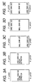
- Figs. 3A, 3B, 3C, 3D, 3E, 3F, 3G, 3H, 3I, 3J and 3K show different grain size distributions in the i-type semiconductor layer of a photovoltaic device according to the invention.
- Fig. 4 is a graph showing the Raman shift of a device obtained in Preliminary Experiment 1.
- Fig. 5 is a graph showing the result obtained by X-ray diffractometry in Preliminary Experiment 1.
- the photovoltaic device comprises a base member 101, an n-type semiconductor layer (or a p-type semiconductor layer) 102, an i-type semiconductor layer 103, a p-type semiconductor layer (or an n-type semiconductor layer) 104, a transparent electrode 105 and a collector electrode 106.
- a metal layer (a back electrode layer) and a transparent conductive layer are arranged on the substrate 101 with an n-type semiconductor layer (or a p-type semiconductor layer) 102 laid thereon.
- the substrate 101 is made of an appropriate conductive or insulating material, which may be metal, resin, glass, a ceramic material or semiconductor bulk. It may have a smooth surface or a finely undulated surface with peaks having a height of 0.1 to 1.0 ⁇ m.
- the substrate 101 is a conductive substrate or some other opaque substrate, light should be allowed to strike the device from the side opposite to the substrate.
- a transparent substrate may be used for the substrate 101 so that light may enter the device through the substrate 101.
- the substrate 101 preferably has the shape of a sheet, a roll formed from a sheet, or a cylinder.
- a conductive material is used for the substrate 101, it is preferably selected from metals including plated steel, NiCr, stainless steel, Al, Cr, Mo, Au, Nb, Ta, V, Ti, Pt, Pb and Sn and alloys of any of them.
- an insulating material may be selected from polyester, polyethylene, polycarbonate, cellulose acetate, polypropylene, polyvinylchloride, polyvinylidenechloride, polystyrene, polyamide and other synthetic resin materials, glass, ceramic materials and paper.
- the substrate 101 may have any appropriate thickness, which can be made very small when the substrate is required to be flexible in the process of manufacturing the photovoltaic device, although it is preferably not less than 10 ⁇ m to ensure a certain degree of mechanical strength.
- the surface of the substrate 101 may be chemically etched or jaggedly cut in order to provide the substrate 101 with undulations on the surface (texture the surface). More specifically, the surface is treated to produce undulations under a controlled manner by means of chemical surface treatment such as chemical polishing or electrolytic polishing or mechanical polishing using diamond, carborundum or alundum and thereafter etched to eliminate multiply undulated areas.
- chemical surface treatment such as chemical polishing or electrolytic polishing or mechanical polishing using diamond, carborundum or alundum and thereafter etched to eliminate multiply undulated areas.
- a continuous strip of substrate may be used for a continuous film forming operation. If such is the case, a continuous strip of a flexible material such as stainless steel or polyimide may suitably be used for the purpose of the invention.
- the back electrode layer is an electrode layer formed on the side of the device opposite to the side from which light enters as viewed from the semiconductor layers.
- the back electrode layer serves as an electrode and, at the same time, as a reflection layer for reflecting the light that has been transmitted through the semiconductor layers so that it may be reutilized by the semiconductor layers.
- the back electrode layer is preferably made of metal selected from gold, silver, copper, aluminum, nickel, iron, chromium, molybdenum, tungsten, titanium, cobalt, tantalum, niobium and zirconium or an alloy such as stainless steel or AlSi, of which aluminum, copper, silver and gold are highly preferably because of their high reflectivity.
- the back electrode layer can be formed by vapor deposition, sputtering, plating, electrolytic deposition using aqueous solution or printing.
- the back electrode layer preferably has a thickness of 10 nm to 5,000 nm.
- the back electrode layer may have a multilayer structure of a plurality of layers. If the substrate 101 is conductive, the back electrode layer may be omitted. However, the use of a back electrode layer is a prerequisite when the substrate 101 is made of an insulating material.
- the transparent conductive layer is arranged between the back electrode layer and the semiconductor layers in order to increase the irregular reflection at the back electrode layer. More specifically, light is trapped in the photovoltaic device and made to follow a prolonged optical path in the semiconductor layers to increase the short-circuit current (Jsc) of the photovoltaic device by the textured surface of the back electrode layer that irregularly reflects light and the transparent conductive layer that reflects light multiply. Additionally, the transparent conductive layer plays the role of preventing the metal of the back electrode layer from diffusing or migrating into the semiconductor layers to shunt the photovoltaic device. It also prevents any short-circuiting from taking place due to the flaws in the semiconductor layers such as pin holes if it is made to show an appropriate level of resistance.
- the electric conductivity of the transparent conductive layer is between 10 -8 (1/ ⁇ cm) and 10 -1 (1/ ⁇ cm).
- the transparent conductive layer is required to show a high transmittance. Preferably, it passes 80% or more, preferably 85% or more, most preferably 90% or more, of light with a wavelength of longer than 650 nm that enters it.
- the transparent conductive layer may have an appropriate thickness depending on the refractivity of the material to be used and may suitably be from 50 nm to 10 ⁇ m.
- the transparent conductive layer is formed from an conductive oxide such as ZnO, ITO (indium tin oxide), In 2 O 3 , SnO 2 , TiO 2 , CdO, Cd 2 Sn 4 , Bi 2 O 3 , MoO 3 or Na x WO 3 by means of an appropriate film forming technique selected from vapor deposition, sputtering, electrolytic deposition, CVD, spray, spin-on, dipping and plating.
- a conductivity modifying agent may be added to the oxide.
- the process of forming the layer is conducted at temperature 200°C or more. The textured effect of the layer can be improved by etching the surface with weak acid after the layer is formed.
- the material to be used for the semiconductor layers according to the invention is selected from the IV group elements such as Si, C and Ge and alloys thereof including SiGe, SiC and SiSn.
- the semiconductor layers of a photovoltaic device are made of a material selected from non-single crystal semiconductors prepared by using any of the IV group elements and their alloys including a-Si:H (hydrogenated amorphous silicon), a-Si:F, a-Si:H:F, a-SiGe:H, a-SeGe:F, a-SiGe:H:F, a-SiC:H, a-SiC:F, a-SiC:H:F.
- the semiconductor layers can be controlled for valence electrons and the forbidden band width.
- the compound material of the semiconductor layers is made to contain a valence electron control agent and/or a forbidden band width control agent and introduced into the film forming space solely or as a diluted or non-diluted mixture source gas containing it and other film depositing materials.
- Each of the semiconductor layers is doped at least partly to the p-type and the n-type to form at least one pin-structure. Then, a stacked cell structure is produced by laying a plurality of pin-structures.
- Japanese Patent Application Laid-Open No. 62-209871 discloses a technique of gradually increasing the degree of microcrystallization of the non-single crystal i-type semiconductor layer toward the p-type semiconductor layer or the n-type semiconductor layer in order to improve the junctioning effect of the p/i or n/i interface particularly when the p-type semiconductor layer or the n-type semiconductor layer is made of microcrystalline silicon.
- the disclosed technique is simply intended to increase the degree of crystallization at the p/i or n/i interface of an amorphous i-type semiconductor layer and the patent application does not disclose anything about the crystal grain size distribution of the i-type semiconductor layer.
- the crystal grain size and the degree of crystallization are totally different factors in the semiconductor layers and either of them cannot be unequivocally defined by defining the other.
- the quantum effect, the multiple reflection effect and the effect of controlling the diffusion length of electric current carriers in a pin-type solar cell can be controlled highly effectively by controlling the crystal grain size if compared with any instance where only the degree of crystallization is controlled.
- the degree of crystallization simply refers to the extent to which the semiconductor material is found in the form of crystals.
- the semiconductor may contain crystals that are very small or unnecessarily large or a mixture of ordinarily-sized crystals and extremely large crystals produced as a result of abnormal growth.
- a photovoltaic device comprising deposited layers that have been controlled only in terms of the degree of crystallization may operate effectively to some extent, it will be far from satisfactory from the viewpoint of the quantum effect, the multiple reflection effect and the effect of controlling the diffusion length of electric current carriers that can be realized by controlling the grain size.
- Japanese Patent Application Laid-Open No. 63-58974 discloses a method of forming a p-type semiconductor layer from a crystalline part (p1) and a amorphous part (p2) and gradually decreasing the degree of crystallization of the crystalline part (p1) toward the amorphous part (p2).
- this method is simply intended to change the extent of crystallinity of the p-type semiconductor layer that serves as an electrode layer and the patent application does not refer to anything about the crystal grain size distribution in the i-type semiconductor layer having a region of photoelectric conversion. Therefore, again, the technique disclosed in the above identified patent application is totally different particularly in terms of objects and effects from the method of the present invention for controlling the crystal grain size distribution to make it to be not uniform but found certain numerical ranges.
- the i-type semiconductor layer shows a uniform grain size distribution in a layer as shown in Fig. 3A or 3B. While microcrystalline silicon still has physical properties to be clarified, it typically shows a light absorption coefficient far greater than single crystal silicon. This may be attributable to the quantum effect due to the grain size of microcrystalline particle (as it is possible to produce a quantum effect by controlling the grain size to improve the light absorption coefficient form that of large crystals) and the effect of multiple reflection of light among crystal grains (that can be regulated by controlling the grain size and hence the reflective surface size and the density of crystal grain boundaries because light is reflected well on crystal grain boundaries).
- the grain size of microcrystalline silicon is preferably hundreds of several angstroms or less in order to make these effects remarkable on the one hand, there is a need for increasing the diffusion length of electric current carriers by raising the grain size of microcrystalline silicon in order to make the device perform well on the other hand (as electric current carriers can diffuse well in a single crystal grain but crystal grain boundaries can provide barriers for the diffusion of electric current carriers). Therefore, the conventional use of uniform grain size distribution in the i-type semiconductor cannot meet the above apparently contradictory two requirements at the same time.
- the inventor of the present invention came to find that the performance of a photovoltaic device can be remarkably improved by optimally controlling the grain size in different regions of the i-type semiconductor layer.
- the grain size distribution of crystal grains in the i-type semiconductor layer is intentionally made to be not uniform in the film thickness direction and/or in the direction along the surface thereof (surface direction).
- Figs. 3C through 3I illustrate combinations of different grain sizes on and near the p/i and n/i interfaces and in other regions.
- the junctioning effect of the p-type semiconductor layer and the n-type semiconductor layer can be improved by using a large grain size on and near the p/i and n/i interfaces.
- the arrangement of Fig. 3C where a large grain size is used in and near the n-type semiconductor layer provides an effect of suppressing the diffusion of phosphor from the n-type semiconductor layer.
- the arrangement of Fig. 3D where a large grain size is used in and near the p-type semiconductor layer provides a remarkable effect of improving the open current voltage and the fill factor because the junctioning effect is improved on the side of receiving incident light.
- Fig. 3E a large grain size is used in and near the p-type and n-type semiconductor layers at the same time to obtain the effect of Fig.
- Figs. 3C through 3E can provide an excellent absorption of light and a large photo-generated electric current because small crystal grains are used in areas other than the p/i and n/i interfaces in the i-type semiconductor layer (the i-type semiconductor bulk region). While the grain size may change discontinuously, it preferably changes continuously because the interface level density can be reduced in the i-type semiconductor to suppress the recombination of photo-generated carriers.
- Figs. 3F through 3H are suited for rapidly forming microcrystals with a relatively large grain size.
- the diffusion length of photo-generated carriers is remarkably increased to produce a pin-type solar cell having excellent fill factors when the crystal grain size is large in the i-type semiconductor layer bulk region.
- the i-type semiconductor layer bulk operates like single crystal silicon when the grain size is increased.
- the film thickness has to be increased to make the solar cell operate satisfactorily.
- a small grain size When a small grain size is used for microcrystals on and near the p/i and n/i interfaces according to the invention, they absorb light and mechanical stresses efficiently and effectively to bring forth the effect of reducing the film thickness of i-type semiconductor layer bulk of crystals having a large grain size and, at the same time, suppressing any defects that can be caused by the difference in the expansion coefficient between the p-type semiconductor layer and the n-type semiconductor layer.
- the grain size of the p-type semiconductor layer or the n-type semiconductor layer is made considerably smaller than that of the i-type semiconductor layer bulk, the small grain size region near the interface can alleviate the mismatch that can occur on the junction.
- the small grain size region may be located on the side of the n/i interface as shown in Fig.
- the grain size may change discontinuously, it preferably changes continuously because the interface level density can be reduced in the i-type semiconductor to suppress the recombination of photo-generated carriers.
- the grain size may preferably be not uniform in the surface direction.
- the grain size may change discontinuously, it preferably changes continuously because the interface level density can be reduced in the i-type semiconductor layer to suppress the recombination of photo-generated carriers.
- collector electrodes are arranged at regular intervals. Therefore, the efficiency of collecting photo-generated carriers can be improved by arranging cyclically and regularly small and large grains in the surface direction in such a way that large crystal grains are found under the collector electrodes.
- the grain size may change discontinuously, it preferably changes continuously because the interface level density can be reduced in the i-type semiconductor layer to suppress the recombination of photo-generated carriers.
- the hydrogen content of the region having a maximum average grain size in the i-type semiconductor layer is preferably smaller than that of the remaining regions. More preferably, the hydrogen content of the region having a maximum average grain size in the i-type semiconductor layer is 10% or less and that of the remaining regions in the i-type semiconductor layer is between 3 and 20%. Besides, the ratio of the smallest average grain size to the largest average grain size in the i-type semiconductor layer is preferably 0.9 or less. Additionally, the non-single crystal silicon is constituted by microcrystalline silicon having a minimum average grain size between 20 angstroms and 1 ⁇ m and microcrystalline silicon or polycrystalline silicon having a maximum average grain size between 50 angstroms and 10mm.
- the dopant concentration in the i-type semiconductor layer is 2 ⁇ 10 17 cm -3 or less on and near the n/i interface.
- the n-type and/or p-type semiconductor layers comprise microcrystalline silicon.
- an i-type amorphous silicon interface layer is arranged between the i-type semiconductor layer and the n-type and/or between the i-type semiconductor layer and the p-type semiconductor layer.
- the non-single crystal silicon is preferably formed under pressure by high frequency plasma CVD with a frequency between 50 and 2,450 MHz, a forming pressure between 0.001 and 0.5 Torr and a making current density between 0.001 and 0.5 W/cm 3 .
- the effects of the present invention can be enhanced by controlling the grain size and the hydrogen content depending on the characteristics of the solar cell to be formed and the productivity of manufacturing solar cells.
- a relatively high hydrogen content may well be selected within the range as defined above for the purpose of the invention.
- the hydrogen content may well be reduced within the rage as defined above for the purpose of the invention.
- a relatively high frequency and a large making current density may well be selected within the respective ranges as defined above for the purpose of the invention.
- the base material of the doped layer is a semiconductor material such as amorphous silicon or microcrystalline silicon.
- Amorphous (as simply expressed by a-) silicon type semiconductor materials that can be used for the purpose of the invention may be selected from a-Si, a-SiC, a-SiO, a-SiN, a-SiCO, a-SiON, a-SiNC and a-SiCON.
- the base material may be an amorphous silicon semiconductor containing microcrystalline silicon.
- the rate of introducing a valence electron control agent in order to produce a p-or n- conduction type is preferably between 1,000 ppm and 10 %.
- Hydrogen (H, D) and fluorine operate to compensate dangling bonds and improve the doping effect.
- the content of hydrogen and fluorine is optimally between 0.1 and 30 atom%.
- Carbon, oxygen and nitrogen are introduced to show a concentration between 0.1 ppm and 20 % and between 0.1 ppm and 1 % when a low concentration is desired.
- the activation energy level is preferably 0.2 eV or less and the specific electric resistance is preferably 100 ⁇ cm or less, most preferably 1 ⁇ cm or less.
- the i-type semiconductor layer takes the most important role in a photovoltaic device according to the invention as it generates and transports photo-excited carrier.
- Non-single crystal silicon that can be used for the purpose of the invention is formed by high frequency plasma CVD with a frequency range between 13.56 MHz and 2.45 GHz and its absorption coefficient shows a photon energy dependency more on amorphous silicon on the high energy side and on crystalline silicon on the low energy side.
- the performance of a pin-type solar cell is improved by making the grain size distribution of crystal grains in the i-type semiconductor layer to be not uniform. Therefore, any of the arrangements illustrated in Figs. 3C through 3K can preferably be used for the purpose of the invention.
- the hydrogen content of the region having a maximum average grain size in the i-type semiconductor layer is preferably smaller than the hydrogen content of the remaining regions in the i-type semiconductor layer. More preferably, the hydrogen content of the region having a maximum average grain size in the i-type semiconductor layer is 10 % or less and that of the remaining regions in the i-type semiconductor layer is between 3 and 20 %. Besides, the ratio of the smallest average grain size to the largest average grain size in the i-type semiconductor layer is preferably 0.9 or less. Additionally, the non-single crystal silicon is constituted by microcrystalline silicon having a minimum average grain size between 20 angstroms and 1 ⁇ m and microcrystalline silicon or polycrystalline silicon having a maximum average grain size between 50 angstroms and 10 mm.
- the n-type semiconductor layer is substantially undoped on and near the n/i interface.
- the n-type and/or p-type semiconductor layers comprise microcrystalline silicon.
- an i-type amorphous silicon interface layer is arranged between the i-type semiconductor layer and the n-type and/or between the i-type semiconductor layer and the p-type semiconductor layer.
- the non-single crystal silicon is preferably formed under pressure by high frequency plasma CVD with a frequency between 50 and 2,450 MHz, a forming pressure between 0.001 and 0.5 Torr and a making current density between 0.001 and 0.5 W/cm 3 .
- the transparent electrode 105 can be made to operate as an anti-reflection film by selecting an appropriate film thickness for it.
- the transparent electrode layer is formed from a material such as ZnO, ITO (indium tin oxide), In 2 O 3 or SnO 2 by means of an appropriate film forming technique selected from vapor deposition, CVD, spray, spin-on and immersion.
- a conductivity modifying agent may be added to the compound.
- Substances that can suitably be used for modifying the conductivity include Al, In, B, Ga, Si and F when the transparent electrode is made of ZnO.
- a substance selected from Sn, F, Te, Ti, Sb and Pb can suitably be used when the transparent electrode is made of In 2 O 3 .
- a substance selected from F, Sb, P, As, In, Tl, Te, W, Cl, Br and I can suitably be used when the transparent electrode is made of SnO 2 .
- the transparent electrode is required to show a high transmittance. Preferably, it passes 85 % or more of light at a wavelength of 550 nm that enters it.
- the resistivity of the transparent electrode layer is 5 ⁇ 10 -3 ⁇ cm or less, more preferably 1 ⁇ 10 -3 ⁇ cm or less.
- the collector electrode 106 is provided to improve the collecting efficiency. It may be formed by producing a pattern of the electrode metal by sputtering using a mask, by printing with conductive paste or solder paste or by bonding a metal wire with conductive paste.
- a protective layer may be formed on the both surfaces of the photovoltaic device. Additionally, a reinforcing material such as sheet steel may be used with the protective layer.
- a photoelectric transducer according to the invention has a configuration essentially identical with the one described above.
- a semiconductor thin film forming apparatus as shown in Fig. 2 was used.
- Substrate 201 is held to an upper portion of the inner wall of the thin film forming apparatus and heated to desired temperature by means of heater 202.
- Source gases are introduced into the apparatus by way of gas introducing pipe 209 and valve 210.
- Source gases were highly refined gases including SiH 4 gas, PH 3 /H 2 gas (dilution: 2 %), B 2 H 6 /H 2 gas (dilution: 2 %) and H 2 gas.
- power sources with a microwave frequency power source 203
- VHF power source 205
- an RF power source 207
- reference numeral 204 denotes a microwave introducing window and reference numeral 206 denotes a VHF electrode and reference numeral 208 denotes an RF electrode.
- a monolayer film of non-doped microcrystalline silicon was formed and tested.
- the substrate was formed by depositing ZnO to a thickness of 0.5 ⁇ m on a 0.5 mm thick stainless steel plate by sputtering method.
- an i-type microcrystalline silicon film was formed by deposition to a thickness about 2 ⁇ m under the conditions listed in Table 1 (for high speed deposition of small grain size microcrystalline silicon).
- the diffraction peak was slightly broad to suggest that the formed film was a mixture of microcrystalline silicon and amorphous silicon.
- the hydrogen content obtained by computation using the infrared absorption spectrum at and near the wave number of 2,100 cm -1 obtained by reflection infrared absorption was about 6 %.
- a microcrystalline silicon film was formed to a thickness of about 2 ⁇ m on a substrate same as that of Preliminary Experiment 1 under the conditions listed in Table 2 below (microcrystalline silicon having a large grain size, low speed deposition).
- the microcrystalline silicon film formed in ⁇ Preliminary Experiment 2 ⁇ was tested for evaluation by means of Raman scattering and X-ray diffraction.
- the Raman shift obtained by Raman scattering showed a sharp peak at the wave number of 520 cm -1 to correspond to microcrystalline silicon.
- the estimated grain size was about 200 angstroms for (111) plane.
- the diffraction peak was slightly broad to suggest that the formed film was a mixture of microcrystalline silicon and amorphous silicon, although the crystallinity of the product seemed to be better than that of ⁇ Preliminary Experiment 2 ⁇ .
- the hydrogen content obtained by computation using the infrared absorption spectrum at and near the wave number of about 2,100 cm -1 obtained by reflection infrared absorption was about 4 %.
- a solar cell having a configuration of Fig. 1 was prepared by using a film forming apparatus as shown in Fig. 2.
- a substrate was prepared.
- a sheet of stainless steel with a thickness of 0.5 mm and a surface area of 50 ⁇ 50 mm 2 was immersed into a mixture of acetone and isopropylalcohol, cleansed with supersonic waves and dried with hot air.
- an Ag film having a textured structure was deposited on the substrate at 300°C to a film thickness of 0.8 ⁇ m by DC magnetron sputtering and thereafter a ZnO transparent electroconductive film having a textured structure was deposited at 300°C to a film thickness of 4.0 ⁇ m also by DC magnetron sputtering.
- a pin structure was formed on the ZnO transparent conductive film by means of a deposition apparatus.
- An n-type semiconductor layer was deposited to a film thickness of about 200 angstroms in a film forming apparatus (not shown) by means of RF waves under the conditions of Table 3.
- An i-type semiconductor layer was deposited to a film thickness of about 1.0 ⁇ m in the film forming apparatus of Fig. 2 by using both VHF (high frequency of 105MHz) and RF (high frequency of 13.56MHz) waves under the conditions of Table 1 (for small grain size crystals).
- a p-type semiconductor layer was deposited to a film thickness of about 100 angstroms by means of RF waves under the conditions of Table 4.
- n-type semiconductor layer n-type microcrystalline silicon: film thickness 200 angstroms
- gas flow rate SiH 4 /H 2 10 %)
- 4.0 sccm PH 3 /H 2 2 %)
- 1.0 sccm H 2 100 sccm forming pressure 1.0 Torr forming temperature 230°C RF (13.56 MHz) power 15 W forming rate 0.4 angstroms/second film forming conditions for p-type semiconductor layer (p-type microcrystalline silicon: film thickness 100 angstroms) gas flow rate SiH 4 /H 2 (10 %) 1.0 sccm BF 3 /H 2 (2 %) 0.2 sccm H 2 35 sccm forming pressure 2.0 Torr forming temperature 170°C RF (13.56 MHz) power 33 W forming rate 0.6 angstroms/second
- a transparent electrode of ITO was deposited to a thickness of about 600 angstroms by sputtering using an ITO target.
- a collector electrode of Au was deposited to a thickness of about 8,000 angstroms by vacuum evaporation using electron beams.
- the pin type solar cell will be referred to as (Cell-1) hereinafter (which corresponds to Fig. 3A).
- a solar cell was prepared under the conditions as listed above for ⁇ Experiment Example 1 ⁇ except that the i-type semiconductor layer was formed by deposition to a thickness of about 1.0 ⁇ m under the conditions of Table 2 (for large grain size).
- This solar cell will be referred to as (Cell-2) hereinafter (which corresponds to Fig. 3B).
- a solar cell was prepared under the conditions as listed above for ⁇ Experiment Example 1 ⁇ except that the i-type semiconductor layer was formed only for an area near the n-type semiconductor layer by deposition to a thickness of about 1,000 angstroms under the conditions of Table 2 (for large grain size) and subsequently for the remaining area to a thickness of about 9,000 angstroms under the conditions of Table 1 (for small grain size).
- This solar cell will be referred to as (Cell-3) hereinafter (which corresponds to Fig. 3C).
- a solar cell was prepared under the conditions as listed above for ⁇ Experiment Example 1 ⁇ except that the i-type semiconductor layer was formed by deposition firstly on the n-type semiconductor layer to a thickness of about 9,000 angstroms under the conditions of Table 1 (for small grain size) and subsequently only for an area near the p-type semiconductor layer to a thickness of about 1,000 angstroms under the conditions of Table 2 (for large grain size).
- This solar cell will be referred to as (Cell-4) hereinafter (which corresponds to Fig. 3D).
- a solar cell was prepared under the conditions as listed above for ⁇ Experiment Example 1 ⁇ except that the i-type semiconductor layer was formed by deposition firstly on the n-type semiconductor layer to a thickness of about 1,000 angstroms under the conditions of Table 2 (for large grain size), secondly to a thickness of about 8,000 angstroms under the conditions of Table 1 (for small grain size) and subsequently only for an area near the p-type semiconductor layer to a thickness of about 1,000 angstroms under the conditions of Table 2 (for large grain size).
- This solar cell will be referred to as (Cell-5) hereinafter (which corresponds to Fig. 3E).
- a solar cell was prepared under the conditions as listed above for ⁇ Experiment Example 1 ⁇ except that the i-type semiconductor layer was formed only for an area near the n-type semiconductor layer by deposition to a thickness of about 1,000 angstroms under the conditions of Table 1 (for small grain size) and subsequently for the remaining area to a thickness of about 9,000 angstroms under the conditions of Table 2 (for large grain size).
- This solar cell will be referred to as (Cell-6) hereinafter (which corresponds to Fig. 3F).
- a solar cell was prepared under the conditions as listed above for ⁇ Experiment Example 1 ⁇ except that the i-type semiconductor layer was formed by deposition firstly on the n-type semiconductor layer to a thickness of about 9,000 angstroms under the conditions of Table 2 (for large grain size) and subsequently only for an area near the p-type semiconductor layer to a thickness of about 1,000 angstroms under the conditions of Table 1 (for small grain size).
- This solar cell will be referred to as (Cell-7) hereinafter (which corresponds to Fig. 3G).
- a solar cell was prepared under the conditions as listed above for ⁇ Experiment Example 1 ⁇ except that the i-type semiconductor layer was formed by deposition firstly on the n-type semiconductor layer to a thickness of about 1,000 angstroms under the conditions of Table 1 (for small grain size), secondly to a thickness of about 8,000 angstroms under the conditions of Table 2 (for large grain size) and subsequently only for an area near the p-type semiconductor layer to a thickness of about 1,000 angstroms under the conditions of Table 1 (for small grain size).
- This solar cell will be referred to as (Cell-8) hereinafter (which corresponds to Fig. 3H).
- a solar cell was prepared under the conditions as listed above for ⁇ Experiment Example 1 ⁇ except that the i-type semiconductor layer was formed on the n-type semiconductor layer by repeating 20 cycles of a first i-type unit layer formed under the conditions of Table 1 (for small grain size) and a second i-type unit layer formed under the conditions of Table 2 (for large grain size).
- This solar cell will be referred to as (Cell-9) hereinafter (which corresponds to Fig. 3I).
- a solar cell was prepared under the conditions as listed above for ⁇ Experiment Example 1 ⁇ except that the i-type semiconductor layer was formed in a manner as described below. After forming the n-type semiconductor layer, it was masked and the i-type semiconductor layer was formed to a thickness of 10,000 angstroms as stripes extending along the plane at regular intervals of 5 mm under the conditions of Table 1 (for small grain size). Then, the n-type semiconductor layer was masked differently so that the gaps among the stripes of the i-type semiconductor layer were filled also with the i-type semiconductor layer formed to a thickness of 10,000 angstroms under the conditions of Table 2 (for large grain size).
- This solar cell will be referred to as (Cell-10) hereinafter (which corresponds to Fig. 3J).
- a solar cell was prepared under the conditions as listed above for ⁇ Experiment Example 1 ⁇ except that the i-type semiconductor layer was formed in a manner as described below. Only the light receiving section of the i-type semiconductor layer was formed under the conditions of Table 1 (for small grain size) and the areas under the metal electrodes were formed under the conditions of Table 2 (for large grain size). The metal electrodes were arranged at regular intervals of 10 mm and therefore the i-type semiconductor layer was formed along the plane in a cyclic manner under the conditions of Table 1 (for small grain size) and those of Table 2 (for large grain size).
- This solar cell will be referred to as (Cell-11) hereinafter (which corresponds to Fig. 3K).
- Table 5 shows the open current voltage Voc, the short-circuit current density Isc, the fill factor FF, the conversion efficiency ⁇ and the optical stability S (percentage of the reduction in the conversion efficiency after irradiation with 1 SUN for 500 hours) observed for each cell and compared with (Cell-2), which was used as reference. (Characteristics of Cells) cell No.
- Voc Isc FF ⁇ S (Cell-2) 1.00 1.00 1.00 1.00 1.00 1.00 (Cell-1) 0.90 1.31 0.84 0.99 0.95 (Cell-3) 0.92 1.28 0.86 1.01 0.96 (Cell-4) 0.93 1.30 0.88 1.06 0.98 (Cell-5) 0.97 1.30 0.92 1.16 0.99 (Cell-6) 0.98 1.05 1.02 1.05 0.99 (Cell-7) 0.97 1.08 1.02 1.07 0.99 (Cell-8) 0.98 1.11 1.06 1.15 0.99 (Cell-9) 1.05 1.10 1.20 1.39 1.00 (Cell-10) 1.01 1.12 0.98 1.11 0.98 (Cell-11) 1.02 1.30 0.90 1.19 0.96
- each of (Cell-3) through (Cell-5) that had grain sizes larger near the p- and n-interfaces than in the i-type semiconductor layer bulk region showed improved Voc and FF and hence ⁇ of the cell when compared with (Cell-1).
- the optical stability S was also improved in these cells.
- each of (Cell-6) through (Cell-8) that had grain sizes conversely smaller near the p- and n- interfaces than in the i-type semiconductor layer bulk region showed improved Isc and FF and hence ⁇ of the cell when compared with (Cell-2).
- the optical stability S was not significantly reduced in these cells because the small grain size region had a sufficiently small film thickness.
- (Cell-9) that had a cyclically changing grain size showed a remarkably improved FF and hence ⁇ of the cell was also significantly improved.
- specimens of pin type solar cell having a grain size distribution as shown in Fig. 3E were prepared by extensively varying the grain size to see the performance.
- Table 8 shows the obtained result.
- the cell performed well when it comprises microcrystalline silicon having a minimum average grain size between 20 angstroms and 1 ⁇ m and microcrystalline silicon or polycrystalline silicon having a maximum average grain size between 50 angstroms and 10 mm.
- specimens of pin-type solar cell having a grain size distribution as shown in Fig. 3E were prepared by controlling the rate of doping the inside of the n-type semiconductor layer and hence the dopant (phosphor) concentration in an area near the n/i interface in the i-type semiconductor layer.
- the dopant (phosphor) concentration in the area near the n/i interface in the n-type semiconductor layer was observed by means of SIMS after the i-type and p-type semiconductor layers.
- Table 9 shows the obtained result. As seen from Table 9, the cell performed well when the dopant (phosphor) concentration in the area near the n/i interface in the i-type semiconductor layer was 2 ⁇ 10 17 cm -3 or less.
- specimens of pin-type solar cell having a grain size distribution as shown in Fig. 3E were prepared, using microcrystalline silicon for the n-type semiconductor layer and/or the p-type semiconductor layer.
- Table 10 shows the obtained result.
- the fill factor showed a remarkable improvement to make the pin-type cell perform excellently when compared with known cells using amorphous silicon for the n-type semiconductor layer and/or the p-type semiconductor layer.
- specimens of pin-type solar cell having a grain size distribution as shown in Fig. 3E were prepared and a 100 angstrom thick layer of i-type amorphous silicon was inserted into the p/i interface and/or n/i interface of the specimens.
- Table 11 shows the obtained result.
- the open current voltage and the fill factor were remarkably improved by inserting an i-type amorphous silicon layer into the p/i interface and/or n/i interface.
- the performance of the pin-type was also improved.
- Voc FF Open Current Voltage Voc, Fill Factor FF and Conversion Efficiency ⁇ (Relative Value) i-type amorphous silicon interface layer Voc FF ⁇ none 1.00 1.00 1.00 only on n/i interface 1.03 1.05 1.10 only on p/i interface 1.10 1.12 1.29 on both n/i and p/i interfaces 1.13 1.15 1.36
- forming pressure it was found that the use of relatively low pressure within the above defined range can form a highly microcrystalline silicon film although optimal pressure can vary depending on the frequency to be used.
- making power density it was found that the use of a relatively large making power density within the above defined range can improve the film forming rate, although excellent microcrystalline silicon film can be obtained under high speed film forming conditions by selecting appropriate values for the frequency and the forming pressure.
- the above ranges for frequency, forming pressure and making power density are advantageous for forming high quality microcrystalline silicon film at low cost.
- a photovoltaic device and a photoelectric transducer having an excellent photoelectric conversion efficiency and a remarkable optical stability can be manufactured at low cost. Additionally, according to the invention, a photovoltaic device having large area and excellent mass productivity can be prepared by use of high frequency plasma CVD.
- a photovoltaic device and a photoelectric transducer having a pin-structure semiconductor layer formed by superposing a p-type semiconductor layer, an i-type semiconductor layer and an n-type semiconductor layer wherein the i-type semiconductor layer comprises a non-single crystal semiconductor and average grain size distribution of crystal grains of the i-type semiconductor layer is not uniform are provided.
- Methods of manufacturing the photovoltaic device and the photoelectric transducer are also provided.
- the manufacturing methods according to the invention can produce photovoltaic devices and photoelectric transducers having an excellent photoelectric conversion efficiency and a remarkable optical stability at an enhanced rate and at low cost.
Abstract
Description
| gas flow rate | SiH4 | 80 sccm |
| H2 | 2400 sccm | |
| forming pressure | 150 mtorr | |
| forming temperature | 350°C | |
| RF (13.56 MHz) power | 10 W | |
| VHF (105 MHz) power | 500 W | |
| forming rate | ∼20 angstroms/second |
| gas flow rate | SiH4 | 80 sccm, |
| H2 | 2,400 sccm | |
| forming pressure | 150 mtorr | |
| forming temperature | 350°C | |
| RF (13.56 MHz) power | 10 W | |
| VHF (105 MHz) power | 100 W | |
| forming rate | ∼5 angstroms/second |
| film forming conditions for n-type semiconductor layer (n-type microcrystalline silicon: film thickness 200 angstroms) | ||
| gas flow rate | SiH4/H2 (10 %) | 4.0 sccm |
| PH3/H2 (2 %) | 1.0 sccm | |
| H2 | 100 sccm | |
| forming pressure | 1.0 Torr | |
| forming temperature | 230°C | |
| RF (13.56 MHz) power | 15 W | |
| forming rate | 0.4 angstroms/second |
| film forming conditions for p-type semiconductor layer (p-type microcrystalline silicon: film thickness 100 angstroms) | ||
| gas flow rate | SiH4/H2 (10 %) | 1.0 sccm |
| BF3/H2 (2 %) | 0.2 sccm | |
| H2 | 35 sccm | |
| forming pressure | 2.0 Torr | |
| forming temperature | 170°C | |
| RF (13.56 MHz) power | 33 W | |
| forming rate | 0.6 angstroms/second |
| (Characteristics of Cells) | |||||
| cell No. | Voc | Isc | FF | η | S |
| (Cell-2) | 1.00 | 1.00 | 1.00 | 1.00 | 1.00 |
| (Cell-1) | 0.90 | 1.31 | 0.84 | 0.99 | 0.95 |
| (Cell-3) | 0.92 | 1.28 | 0.86 | 1.01 | 0.96 |
| (Cell-4) | 0.93 | 1.30 | 0.88 | 1.06 | 0.98 |
| (Cell-5) | 0.97 | 1.30 | 0.92 | 1.16 | 0.99 |
| (Cell-6) | 0.98 | 1.05 | 1.02 | 1.05 | 0.99 |
| (Cell-7) | 0.97 | 1.08 | 1.02 | 1.07 | 0.99 |
| (Cell-8) | 0.98 | 1.11 | 1.06 | 1.15 | 0.99 |
| (Cell-9) | 1.05 | 1.10 | 1.20 | 1.39 | 1.00 |
| (Cell-10) | 1.01 | 1.12 | 0.98 | 1.11 | 0.98 |
| (Cell-11) | 1.02 | 1.30 | 0.90 | 1.19 | 0.96 |


| Fill Factor FF and Conversion Efficiency η (Relative Value) | ||
| n-type and p-type semiconductor layers | FF | η |
| amorphous silicon for both n and p | 1.00 | 1.00 |
| microcrystalline silicon only for n | 1.05 | 1.08 |
| microcrystalline silicon only for p | 1.20 | 1.13 |
| microcrystalline silicon for both n and p | 1.20 | 1.27 |
| Open Current Voltage Voc, Fill Factor FF and Conversion Efficiency η (Relative Value) | |||
| i-type amorphous silicon interface layer | Voc | FF | η |
| none | 1.00 | 1.00 | 1.00 |
| only on n/i interface | 1.03 | 1.05 | 1.10 |
| only on p/i interface | 1.10 | 1.12 | 1.29 |
| on both n/i and p/i interfaces | 1.13 | 1.15 | 1.36 |
Claims (32)
- A photovoltaic device having a pin-structure semiconductor layer formed by superposing a p-type semiconductor layer, an i-type semiconductor layer and an n-type semiconductor layer, wherein the i-type semiconductor layer comprises a non-single crystal semiconductor and average grain size distribution of crystal grains of the i-type semiconductor layer is not uniform.
- The photovoltaic device according to claim 1, wherein the average grain size distribution of the crystal grains contained in the i-type semiconductor layer is not uniform in the film thickness direction.
- The photovoltaic device according to claim 1, wherein the average grain size of the crystal grains in the i-type semiconductor layer in a region near the interface of the i-type semiconductor layer and the p-type semiconductor layer and/or that of the i-type semiconductor layer and the n-type semiconductor layer is greater than the average grain size of the crystal grains in the remaining regions of the i-type semiconductor layer.
- The photovoltaic device according to claim 1, wherein the average grain size distribution of the crystal grains contained in the i-type semiconductor layer changes cyclically.
- The photovoltaic device according to claim 1, wherein the average grain size distribution of the crystal grains contained in the i-type semiconductor layer is not uniform in the surface direction perpendicular to the film thickness direction.
- The photovoltaic device according to claim 1, wherein the hydrogen content of the region having the largest average grain size in the i-type semiconductor layer is smaller than the hydrogen content of the remaining regions of the i-type semiconductor layer.
- The photovoltaic device according to claim 6, wherein the hydrogen content of the region having the largest average grain size in the i-type semiconductor layer is 10 % or less and the hydrogen content of the remaining regions of the i-type semiconductor is between 3 and 20 %.
- The photovoltaic device according to claim 1, wherein the ratio of the smallest average grain size to the largest average grain size is 0.9 or less.
- The photovoltaic device according to claim 1, wherein the non-single crystal semiconductor comprises microcrystalline semiconductor with the largest average grain size between 20 angstroms and 1 µm, and microcrystalline semiconductor or polycrystalline semiconductor with the largest average grain size between 50 angstroms and 10 mm.
- The photovoltaic device according to claim 1, wherein the non-single crystal semiconductor comprises non-single crystal silicon.
- The photovoltaic device according to claim 1, wherein the dopant concentration in a region in the i-type semiconductor layer located near the interface of the n-type semiconductor is 2 × 1017 cm-3 or less.
- The photovoltaic device according to claim 1, wherein the p-type semiconductor layer and/or the n-type semiconductor layer comprise a microcrystalline semiconductor.
- The photovoltaic device according to claim 1, wherein the i-type semiconductor layer comprises an amorphous semiconductor layer located between the i-type semiconductor layer and the p-type semiconductor layer and/or the n-type semiconductor layer.
- The photovoltaic device according to claim 1, wherein the i-type semiconductor layer is formed by high frequency plasma CVD under the conditions of a frequency between 50 and 2,450 MHz, pressure between 0.001 and 0.5 Torr and a making power density between 0.001 and 0.5 W/cm3.
- A photoelectric transducer having a pin-structure semiconductor layer formed by superposing a p-type semiconductor layer, an i-type semiconductor layer and an n-type semiconductor layer, wherein the i-type semiconductor layer comprises a non-single crystal semiconductor and average grain size distribution of crystal grains of the i-type semiconductor layer is not uniform.
- The photoelectric transducer according to claim 15, wherein the average grain size distribution of the crystal grains contained in the i-type semiconductor layer is not uniform in the film thickness direction.
- The photoelectric transducer according to claim 15, wherein the average grain size of the crystal grains in the i-type semiconductor layer in a region near the interface of the i-type semiconductor layer and the p-type semiconductor layer and/or that of the i-type semiconductor layer and the n-type semiconductor layer is greater than the average grain size of the crystal grains in the remaining regions of the i-type semiconductor layer.
- The photoelectric transducer according to claim 15, wherein the average grain size distribution of the crystal grains contained in the i-type semiconductor layer changes cyclically.
- The photoelectric transducer according to claim 15, wherein the average grain size distribution of the crystal grains contained in the i-type semiconductor layer is not uniform in the surface direction perpendicular to the film thickness direction.
- The photoelectric transducer according to claim 15, wherein the hydrogen content of the region having the largest average grain size in the i-type semiconductor layer is smaller than the hydrogen content of the remaining regions of the i-type semiconductor layer.
- The photoelectric transducer according to claim 20, wherein the hydrogen content of the region having the largest average grain size in the i-type semiconductor layer is 10 % or less and the hydrogen content of the remaining regions of the i-type semiconductor is between 3 and 20 %.
- The photoelectric transducer according to claim 15, wherein the ratio of the smallest average grain size to the largest average grain size is 0.9 or less.
- The photoelectric transducer according to claim 15, wherein the non-single crystal semiconductor comprises microcrystalline semiconductor with the largest average grain size between 20 angstroms and 1 µm, and monocrystalline semiconductor or polycrystalline semiconductor with the largest average grain size between 50 angstroms and 10 mm.
- The photoelectric transducer according to claim 15, wherein the non-single crystal semiconductor comprises non-single crystal silicon.
- The photoelectric transducer according to claim 15, wherein the dopant concentration in a region in the i-type semiconductor layer located near the interface of the n-type semiconductor layer is 2 × 1017 cm-3 or less.
- The photoelectric transducer according to claim 15, wherein the p-type semiconductor layer and/or the n-type semiconductor layer comprise a microcrystalline semiconductor.
- The photoelectric transducer according to claim 15, wherein the i-type semiconductor layer comprises an amorphous semiconductor layer located between the i-type semiconductor layer and the p-type semiconductor layer and/or the n-type semiconductor layer.
- The photoelectric transducer according to claim 15, wherein the i-type semiconductor layer is formed by high frequency plasma CVD under the conditions of a frequency between 50 and 2,450 MHz, pressure between 0.001 and 0.5 Torr and a making power density between 0.001 and 0.5 W/cm3.
- A method of manufacturing a photovoltaic device having a pin-structure semiconductor layer formed by superposing a p-type semiconductor layer, an i-type semiconductor layer and an n-type semiconductor layer, wherein the i-type semiconductor layer is formed by high frequency plasma CVD under the conditions of a frequency between 50 and 2,450 MHz, pressure between 0.001 and 0.5 Torr and a making power density between 0.001 and 0.5 W/cm3.
- The method of manufacturing a photovoltaic device according to claim 29, wherein the average grain size distribution of the crystal grains in the i-type semiconductor layer is made not uniform by changing at least one of the conditions during the i-type semiconductor layer formation.
- A method of manufacturing a photoelectric transducer having a pin-structure semiconductor layer formed by superposing a p-type semiconductor layer, an i-type semiconductor layer and an n-type semiconductor layer, wherein the i-type semiconductor layer is formed by high frequency plasma CVD under the conditions of a frequency between 50 and 2,450 MHz, pressure between 0.001 and 0.5 Torr and a making power density between 0.001 and 0.5 W/cm3.
- The method of manufacturing a photoelectric transducer according to claim 31, wherein the average grain size distribution of the crystal grains in the i-type semiconductor layer is made not uniform by changing at least one of the conditions during the i-type semiconductor layer formation.
Applications Claiming Priority (6)
| Application Number | Priority Date | Filing Date | Title |
|---|---|---|---|
| JP3512697 | 1997-02-19 | ||
| JP3512697 | 1997-02-19 | ||
| JP35126/97 | 1997-02-19 | ||
| JP34661/98 | 1998-02-17 | ||
| JP03466198A JP3754815B2 (en) | 1997-02-19 | 1998-02-17 | Photovoltaic element, photoelectric conversion element, method for producing photovoltaic element, and method for producing photoelectric conversion element |
| JP3466198 | 1998-02-17 |
Publications (3)
| Publication Number | Publication Date |
|---|---|
| EP0860885A2 true EP0860885A2 (en) | 1998-08-26 |
| EP0860885A3 EP0860885A3 (en) | 2000-05-03 |
| EP0860885B1 EP0860885B1 (en) | 2004-09-15 |
Family
ID=26373494
Family Applications (1)
| Application Number | Title | Priority Date | Filing Date |
|---|---|---|---|
| EP98102791A Expired - Lifetime EP0860885B1 (en) | 1997-02-19 | 1998-02-18 | Photovoltaic device, photoelectric transducer and method of manufacturing same |
Country Status (7)
| Country | Link |
|---|---|
| US (1) | US6043427A (en) |
| EP (1) | EP0860885B1 (en) |
| JP (1) | JP3754815B2 (en) |
| KR (1) | KR100340892B1 (en) |
| CN (1) | CN1182591C (en) |
| AU (1) | AU745050B2 (en) |
| DE (1) | DE69826161T2 (en) |
Cited By (14)
| Publication number | Priority date | Publication date | Assignee | Title |
|---|---|---|---|---|
| EP1069625A2 (en) * | 1999-07-14 | 2001-01-17 | Canon Kabushiki Kaisha | Microcrystalline series photovoltaic element, process for the production of said photovoltaic element, building material and power generation apparatus in which said photovoltaic element is used |
| EP1107319A2 (en) * | 1999-11-30 | 2001-06-13 | Sharp Kabushiki Kaisha | Thin film solar cell and fabrication method therefor |
| WO2001071820A2 (en) * | 2000-03-22 | 2001-09-27 | Aegis Semiconductor | A semitransparent optical detector with a transparent conductor and method of making |
| WO2001073857A2 (en) * | 2000-03-27 | 2001-10-04 | Aegis Semiconductor | A semitransparent optical detector including a polycrystalline layer and method of making |
| US6472248B2 (en) | 1999-07-04 | 2002-10-29 | Canon Kabushiki Kaisha | Microcrystalline series photovoltaic element and process for fabrication of same |
| US6670599B2 (en) | 2000-03-27 | 2003-12-30 | Aegis Semiconductor, Inc. | Semitransparent optical detector on a flexible substrate and method of making |
| US6879014B2 (en) | 2000-03-20 | 2005-04-12 | Aegis Semiconductor, Inc. | Semitransparent optical detector including a polycrystalline layer and method of making |
| FR2868598A1 (en) * | 2004-04-05 | 2005-10-07 | Solarforce Soc Par Actions Sim | PROCESS FOR PRODUCING POLYCRYSTALLINE SILICON PLATES |
| US7002697B2 (en) | 2001-08-02 | 2006-02-21 | Aegis Semiconductor, Inc. | Tunable optical instruments |
| US7214872B2 (en) | 2001-09-28 | 2007-05-08 | Sanyo Electric Co., Ltd | Photovoltaic element and photovoltaic device |
| US7221827B2 (en) | 2003-09-08 | 2007-05-22 | Aegis Semiconductor, Inc. | Tunable dispersion compensator |
| EP2017895A2 (en) * | 2007-07-18 | 2009-01-21 | SCHOTT Solar GmbH | Silicon multi-solar cell and method for its manufacture |
| EP2099076A1 (en) * | 2006-12-25 | 2009-09-09 | Sharp Kabushiki Kaisha | Photoelectric converter and method for fabricating the same |
| DE10101035B4 (en) * | 2000-01-13 | 2012-12-06 | Sharp K.K. | Thin-film solar cell, solar cell module and method of manufacturing a thin-film solar cell |
Families Citing this family (38)
| Publication number | Priority date | Publication date | Assignee | Title |
|---|---|---|---|---|
| JPH11233801A (en) * | 1998-02-17 | 1999-08-27 | Canon Inc | Formation of fine crystalline silicon film and photovoltaic device |
| US6495392B2 (en) * | 1999-08-24 | 2002-12-17 | Canon Kabushiki Kaisha | Process for producing a semiconductor device |
| JP2001332749A (en) | 2000-05-23 | 2001-11-30 | Canon Inc | Method for forming semiconductor thin film and amorphous silicon solar cell element |
| AU2001285055A1 (en) * | 2000-08-18 | 2002-03-04 | Midwest Research Institute | High carrier concentration p-type transparent conducting oxide films |
| US20020131668A1 (en) * | 2001-01-23 | 2002-09-19 | Marsh John Haig | Method of manufacturing optical devices and related improvements |
| US6930025B2 (en) * | 2001-02-01 | 2005-08-16 | Canon Kabushiki Kaisha | Transparent conductive film formation process, photovoltaic device production process, transparent conductive film, and photovoltaic device |
| US7517784B2 (en) * | 2001-08-17 | 2009-04-14 | Alliance For Sustainable Energy, Llc | Method for producing high carrier concentration p-Type transparent conducting oxides |
| US20050151131A1 (en) * | 2002-06-11 | 2005-07-14 | Wager John F.Iii | Polycrystalline thin-film solar cells |
| JP4171428B2 (en) * | 2003-03-20 | 2008-10-22 | 三洋電機株式会社 | Photovoltaic device |
| US7285796B2 (en) * | 2004-06-02 | 2007-10-23 | Micron Technology, Inc. | Raised photodiode sensor to increase fill factor and quantum efficiency in scaled pixels |
| WO2006038453A1 (en) * | 2004-10-04 | 2006-04-13 | Kaneka Corporation | Photoelectric converter |
| US7906723B2 (en) * | 2008-04-30 | 2011-03-15 | General Electric Company | Compositionally-graded and structurally-graded photovoltaic devices and methods of fabricating such devices |
| US20070256734A1 (en) * | 2006-05-08 | 2007-11-08 | United Solar Ovonic Llc | Stabilized photovoltaic device and methods for its manufacture |
| JP2008115460A (en) * | 2006-10-12 | 2008-05-22 | Canon Inc | Method for forming semiconductor device and method for forming photovoltaic device |
| JP5315008B2 (en) * | 2007-11-16 | 2013-10-16 | 株式会社半導体エネルギー研究所 | Photoelectric conversion device |
| US20090194155A1 (en) * | 2008-02-01 | 2009-08-06 | Guardian Industries Corp. | Front electrode having etched surface for use in photovoltaic device and method of making same |
| US8076175B2 (en) * | 2008-02-25 | 2011-12-13 | Suniva, Inc. | Method for making solar cell having crystalline silicon P-N homojunction and amorphous silicon heterojunctions for surface passivation |
| US20090211623A1 (en) * | 2008-02-25 | 2009-08-27 | Suniva, Inc. | Solar module with solar cell having crystalline silicon p-n homojunction and amorphous silicon heterojunctions for surface passivation |
| US8652871B2 (en) * | 2008-08-29 | 2014-02-18 | Tel Solar Ag | Method for depositing an amorphous silicon film for photovoltaic devices with reduced light-induced degradation for improved stabilized performance |
| US8022291B2 (en) * | 2008-10-15 | 2011-09-20 | Guardian Industries Corp. | Method of making front electrode of photovoltaic device having etched surface and corresponding photovoltaic device |
| KR20100070753A (en) * | 2008-12-18 | 2010-06-28 | 삼성전자주식회사 | Manufacturing method of photovoltaic devices |
| KR101528455B1 (en) * | 2009-01-12 | 2015-06-10 | 주성엔지니어링(주) | Thin film type Solar Cell and Method for manufacturing the same |
| EP2352180A1 (en) * | 2009-07-13 | 2011-08-03 | Sanyo Electric Co., Ltd. | Thin film solar cell and method for manufacturing same |
| WO2011065687A2 (en) * | 2009-11-24 | 2011-06-03 | 주식회사 티지솔라 | Crystallized solar cell using microcrystalline semiconductor layer and production method for same |
| KR101194243B1 (en) * | 2010-04-20 | 2012-10-29 | 한국철강 주식회사 | Tandem photovoltaic apparatus and method for manufacturing the same |
| JP2013533620A (en) * | 2010-06-25 | 2013-08-22 | テル・ソーラー・アクチェンゲゼルシャフト | Thin-film solar cell having a microcrystalline absorption layer and a passivation layer and method for manufacturing the solar cell |
| DE102010061831A1 (en) * | 2010-11-24 | 2012-05-24 | Fraunhofer-Gesellschaft zur Förderung der angewandten Forschung e.V. | Semiconductor component and method for its production |
| KR20120084177A (en) * | 2011-01-19 | 2012-07-27 | 삼성전자주식회사 | Fabrication method of silicon quantum dot layer and devices fabricated using the same |
| JP5610156B2 (en) * | 2011-01-31 | 2014-10-22 | 日立金属株式会社 | Photoelectric conversion module and method for manufacturing photoelectric conversion module |
| JP5812112B2 (en) * | 2011-12-19 | 2015-11-11 | 株式会社島津製作所 | Radiation detector and manufacturing method thereof |
| JP5583196B2 (en) * | 2011-12-21 | 2014-09-03 | パナソニック株式会社 | Thin film solar cell and manufacturing method thereof |
| KR101453967B1 (en) * | 2012-02-20 | 2014-10-29 | 고려대학교 산학협력단 | Multiple band gab laminating sollar cell and method for build the same |
| US11005000B2 (en) | 2013-12-09 | 2021-05-11 | Avago Technologies International Sales Pte. Limited | Connector for photonic device |
| US9466754B2 (en) * | 2014-07-30 | 2016-10-11 | Sunpower Corporation | Grain growth for solar cells |
| KR102600379B1 (en) * | 2015-12-21 | 2023-11-10 | 상라오 징코 솔라 테크놀러지 디벨롭먼트 컴퍼니, 리미티드 | Solar cell and method for fabricating therefor |
| KR101879363B1 (en) | 2017-01-17 | 2018-08-16 | 엘지전자 주식회사 | Manufacturng method of solar cell |
| CN108987521B (en) * | 2017-05-31 | 2022-02-08 | 安华高科技股份有限公司 | Transducer for converting light energy into electric energy |
| CN111599879B (en) * | 2020-06-11 | 2022-05-31 | 武汉华星光电技术有限公司 | PIN photosensitive device, manufacturing method thereof and display panel |
Citations (3)
| Publication number | Priority date | Publication date | Assignee | Title |
|---|---|---|---|---|
| US4433202A (en) * | 1981-03-30 | 1984-02-21 | Hitachi, Ltd. | Thin film solar cell |
| US5024706A (en) * | 1989-01-21 | 1991-06-18 | Canon Kabushiki Kaisha | Pin heterojunction photovoltaic elements with polycrystal AlP(H,F) semiconductor film |
| US5162239A (en) * | 1990-12-27 | 1992-11-10 | Xerox Corporation | Laser crystallized cladding layers for improved amorphous silicon light-emitting diodes and radiation sensors |
Family Cites Families (5)
| Publication number | Priority date | Publication date | Assignee | Title |
|---|---|---|---|---|
| JPS57187971A (en) * | 1981-05-15 | 1982-11-18 | Agency Of Ind Science & Technol | Solar cell |
| JPS62209871A (en) * | 1986-03-10 | 1987-09-16 | Sanyo Electric Co Ltd | Manufacture of photovoltaic device |
| JPS63258078A (en) * | 1987-04-15 | 1988-10-25 | Mitsubishi Electric Corp | Amorphous photoelectric conversion device |
| DE69410301T2 (en) * | 1993-01-29 | 1998-09-24 | Canon Kk | Process for the production of functional deposited layers |
| US5769963A (en) * | 1995-08-31 | 1998-06-23 | Canon Kabushiki Kaisha | Photovoltaic device |
-
1998
- 1998-02-17 JP JP03466198A patent/JP3754815B2/en not_active Expired - Fee Related
- 1998-02-18 AU AU55372/98A patent/AU745050B2/en not_active Ceased
- 1998-02-18 EP EP98102791A patent/EP0860885B1/en not_active Expired - Lifetime
- 1998-02-18 DE DE69826161T patent/DE69826161T2/en not_active Expired - Lifetime
- 1998-02-19 KR KR1019980005169A patent/KR100340892B1/en not_active IP Right Cessation
- 1998-02-19 US US09/025,794 patent/US6043427A/en not_active Expired - Lifetime
- 1998-02-19 CN CNB981044891A patent/CN1182591C/en not_active Expired - Fee Related
Patent Citations (3)
| Publication number | Priority date | Publication date | Assignee | Title |
|---|---|---|---|---|
| US4433202A (en) * | 1981-03-30 | 1984-02-21 | Hitachi, Ltd. | Thin film solar cell |
| US5024706A (en) * | 1989-01-21 | 1991-06-18 | Canon Kabushiki Kaisha | Pin heterojunction photovoltaic elements with polycrystal AlP(H,F) semiconductor film |
| US5162239A (en) * | 1990-12-27 | 1992-11-10 | Xerox Corporation | Laser crystallized cladding layers for improved amorphous silicon light-emitting diodes and radiation sensors |
Non-Patent Citations (2)
| Title |
|---|
| PATENT ABSTRACTS OF JAPAN vol. 012, no. 065 (E-586), 27 February 1988 (1988-02-27) & JP 62 209871 A (SANYO ELECTRIC CO LTD), 16 September 1987 (1987-09-16) * |
| PATENT ABSTRACTS OF JAPAN vol. 013, no. 078 (E-718), 22 February 1989 (1989-02-22) & JP 63 258078 A (MITSUBISHI ELECTRIC CORP), 25 October 1988 (1988-10-25) * |
Cited By (21)
| Publication number | Priority date | Publication date | Assignee | Title |
|---|---|---|---|---|
| US6472248B2 (en) | 1999-07-04 | 2002-10-29 | Canon Kabushiki Kaisha | Microcrystalline series photovoltaic element and process for fabrication of same |
| EP1069625A3 (en) * | 1999-07-14 | 2007-03-14 | Canon Kabushiki Kaisha | Microcrystalline series photovoltaic element, process for the production of said photovoltaic element, building material and power generation apparatus in which said photovoltaic element is used |
| EP1069625A2 (en) * | 1999-07-14 | 2001-01-17 | Canon Kabushiki Kaisha | Microcrystalline series photovoltaic element, process for the production of said photovoltaic element, building material and power generation apparatus in which said photovoltaic element is used |
| EP1107319A2 (en) * | 1999-11-30 | 2001-06-13 | Sharp Kabushiki Kaisha | Thin film solar cell and fabrication method therefor |
| EP1107319A3 (en) * | 1999-11-30 | 2004-06-23 | Sharp Kabushiki Kaisha | Thin film solar cell and fabrication method therefor |
| DE10101035B4 (en) * | 2000-01-13 | 2012-12-06 | Sharp K.K. | Thin-film solar cell, solar cell module and method of manufacturing a thin-film solar cell |
| US6879014B2 (en) | 2000-03-20 | 2005-04-12 | Aegis Semiconductor, Inc. | Semitransparent optical detector including a polycrystalline layer and method of making |
| WO2001071820A2 (en) * | 2000-03-22 | 2001-09-27 | Aegis Semiconductor | A semitransparent optical detector with a transparent conductor and method of making |
| US6670599B2 (en) | 2000-03-27 | 2003-12-30 | Aegis Semiconductor, Inc. | Semitransparent optical detector on a flexible substrate and method of making |
| WO2001071820A3 (en) * | 2000-03-27 | 2002-02-14 | Aegis Semiconductor | A semitransparent optical detector with a transparent conductor and method of making |
| WO2001073857A3 (en) * | 2000-03-27 | 2002-01-31 | Aegis Semiconductor | A semitransparent optical detector including a polycrystalline layer and method of making |
| WO2001073857A2 (en) * | 2000-03-27 | 2001-10-04 | Aegis Semiconductor | A semitransparent optical detector including a polycrystalline layer and method of making |
| US7002697B2 (en) | 2001-08-02 | 2006-02-21 | Aegis Semiconductor, Inc. | Tunable optical instruments |
| US7214872B2 (en) | 2001-09-28 | 2007-05-08 | Sanyo Electric Co., Ltd | Photovoltaic element and photovoltaic device |
| US7221827B2 (en) | 2003-09-08 | 2007-05-22 | Aegis Semiconductor, Inc. | Tunable dispersion compensator |
| WO2005101527A1 (en) * | 2004-04-05 | 2005-10-27 | Solarforce | Method for making polysilicon films |
| FR2868598A1 (en) * | 2004-04-05 | 2005-10-07 | Solarforce Soc Par Actions Sim | PROCESS FOR PRODUCING POLYCRYSTALLINE SILICON PLATES |
| EP2099076A1 (en) * | 2006-12-25 | 2009-09-09 | Sharp Kabushiki Kaisha | Photoelectric converter and method for fabricating the same |
| EP2099076A4 (en) * | 2006-12-25 | 2013-07-03 | Sharp Kk | Photoelectric converter and method for fabricating the same |
| EP2017895A2 (en) * | 2007-07-18 | 2009-01-21 | SCHOTT Solar GmbH | Silicon multi-solar cell and method for its manufacture |
| EP2017895A3 (en) * | 2007-07-18 | 2014-02-12 | SCHOTT Solar AG | Silicon multi-solar cell and method for its manufacture |
Also Published As
| Publication number | Publication date |
|---|---|
| JP3754815B2 (en) | 2006-03-15 |
| JPH10294484A (en) | 1998-11-04 |
| US6043427A (en) | 2000-03-28 |
| CN1182591C (en) | 2004-12-29 |
| KR100340892B1 (en) | 2002-08-22 |
| AU5537298A (en) | 1998-08-27 |
| EP0860885B1 (en) | 2004-09-15 |
| EP0860885A3 (en) | 2000-05-03 |
| AU745050B2 (en) | 2002-03-07 |
| DE69826161D1 (en) | 2004-10-21 |
| KR19980071510A (en) | 1998-10-26 |
| DE69826161T2 (en) | 2005-10-27 |
| CN1191395A (en) | 1998-08-26 |
Similar Documents
| Publication | Publication Date | Title |
|---|---|---|
| EP0860885B1 (en) | Photovoltaic device, photoelectric transducer and method of manufacturing same | |
| US6100466A (en) | Method of forming microcrystalline silicon film, photovoltaic element, and method of producing same | |
| JP4208281B2 (en) | Multilayer photovoltaic device | |
| JP3768672B2 (en) | Multilayer photovoltaic device | |
| KR100251070B1 (en) | Photovoltaic device | |
| JP2984595B2 (en) | Photovoltaic element | |
| EP0895291B1 (en) | Photovoltaic element and method of producing the same | |
| EP1100130B3 (en) | Silicon-base thin-film photoelectric device | |
| US6488995B1 (en) | Method of forming microcrystalline silicon film, method of fabricating photovoltaic cell using said method, and photovoltaic device fabricated thereby | |
| EP0831538A2 (en) | Photovoltaic element having a specific doped layer | |
| JP2004165394A (en) | Stacked photovoltaic element | |
| JP3679595B2 (en) | Photovoltaic element and manufacturing method thereof | |
| JPH11103082A (en) | Photosensor and manufacture thereof | |
| JP3710312B2 (en) | Photovoltaic element and manufacturing method thereof | |
| JP3659511B2 (en) | Photovoltaic element | |
| JPH11233443A (en) | Forming method of microcrystal silicon film, photovoltaic element and forming equipment of semiconductor film | |
| JP2007189266A (en) | Stacked photovoltaic element | |
| JP3072831B2 (en) | Photovoltaic element | |
| JPH09191119A (en) | Manufacture of photovolataic element | |
| JPH06318716A (en) | Photovoltaic element |
Legal Events
| Date | Code | Title | Description |
|---|---|---|---|
| PUAI | Public reference made under article 153(3) epc to a published international application that has entered the european phase |
Free format text: ORIGINAL CODE: 0009012 |
|
| AK | Designated contracting states |
Kind code of ref document: A2 Designated state(s): CH DE IT LI |
|
| AX | Request for extension of the european patent |
Free format text: AL;LT;LV;MK;RO;SI |
|
| PUAL | Search report despatched |
Free format text: ORIGINAL CODE: 0009013 |
|
| RIC1 | Information provided on ipc code assigned before grant |
Free format text: 7H 01L 31/036 A, 7H 01L 31/075 B, 7H 01L 31/105 B, 7H 01L 31/20 B |
|
| AK | Designated contracting states |
Kind code of ref document: A3 Designated state(s): AT BE CH DE DK ES FI FR GB GR IE IT LI LU MC NL PT SE |
|
| AX | Request for extension of the european patent |
Free format text: AL;LT;LV;MK;RO;SI |
|
| 17P | Request for examination filed |
Effective date: 20001002 |
|
| AKX | Designation fees paid |
Free format text: CH DE IT LI |
|
| 17Q | First examination report despatched |
Effective date: 20011026 |
|
| GRAP | Despatch of communication of intention to grant a patent |
Free format text: ORIGINAL CODE: EPIDOSNIGR1 |
|
| GRAS | Grant fee paid |
Free format text: ORIGINAL CODE: EPIDOSNIGR3 |
|
| GRAA | (expected) grant |
Free format text: ORIGINAL CODE: 0009210 |
|
| AK | Designated contracting states |
Kind code of ref document: B1 Designated state(s): CH DE IT LI |
|
| REG | Reference to a national code |
Ref country code: CH Ref legal event code: EP |
|
| REF | Corresponds to: |
Ref document number: 69826161 Country of ref document: DE Date of ref document: 20041021 Kind code of ref document: P |
|
| REG | Reference to a national code |
Ref country code: CH Ref legal event code: NV Representative=s name: BOVARD AG PATENTANWAELTE |
|
| PLBE | No opposition filed within time limit |
Free format text: ORIGINAL CODE: 0009261 |
|
| STAA | Information on the status of an ep patent application or granted ep patent |
Free format text: STATUS: NO OPPOSITION FILED WITHIN TIME LIMIT |
|
| 26N | No opposition filed |
Effective date: 20050616 |
|
| REG | Reference to a national code |
Ref country code: CH Ref legal event code: PFA Owner name: CANON KABUSHIKI KAISHA Free format text: CANON KABUSHIKI KAISHA#30-2, 3-CHOME, SHIMOMARUKO, OHTA-KU#TOKYO (JP) -TRANSFER TO- CANON KABUSHIKI KAISHA#30-2, 3-CHOME, SHIMOMARUKO, OHTA-KU#TOKYO (JP) |
|
| PGFP | Annual fee paid to national office [announced via postgrant information from national office to epo] |
Ref country code: DE Payment date: 20140228 Year of fee payment: 17 Ref country code: CH Payment date: 20140221 Year of fee payment: 17 |
|
| PGFP | Annual fee paid to national office [announced via postgrant information from national office to epo] |
Ref country code: IT Payment date: 20140204 Year of fee payment: 17 |
|
| REG | Reference to a national code |
Ref country code: DE Ref legal event code: R119 Ref document number: 69826161 Country of ref document: DE |
|
| REG | Reference to a national code |
Ref country code: CH Ref legal event code: PL |
|
| PG25 | Lapsed in a contracting state [announced via postgrant information from national office to epo] |
Ref country code: LI Free format text: LAPSE BECAUSE OF NON-PAYMENT OF DUE FEES Effective date: 20150228 Ref country code: CH Free format text: LAPSE BECAUSE OF NON-PAYMENT OF DUE FEES Effective date: 20150228 |
|
| PG25 | Lapsed in a contracting state [announced via postgrant information from national office to epo] |
Ref country code: IT Free format text: LAPSE BECAUSE OF NON-PAYMENT OF DUE FEES Effective date: 20150218 |
|
| PG25 | Lapsed in a contracting state [announced via postgrant information from national office to epo] |
Ref country code: DE Free format text: LAPSE BECAUSE OF NON-PAYMENT OF DUE FEES Effective date: 20150901 |