EP0848342A2 - Intergrated circuit design method, database apparatus for designing integrated circuit and integrated circuit design support apparatus - Google Patents
Intergrated circuit design method, database apparatus for designing integrated circuit and integrated circuit design support apparatus Download PDFInfo
- Publication number
- EP0848342A2 EP0848342A2 EP97121676A EP97121676A EP0848342A2 EP 0848342 A2 EP0848342 A2 EP 0848342A2 EP 97121676 A EP97121676 A EP 97121676A EP 97121676 A EP97121676 A EP 97121676A EP 0848342 A2 EP0848342 A2 EP 0848342A2
- Authority
- EP
- European Patent Office
- Prior art keywords
- design
- features
- description data
- level
- generating
- Prior art date
- Legal status (The legal status is an assumption and is not a legal conclusion. Google has not performed a legal analysis and makes no representation as to the accuracy of the status listed.)
- Ceased
Links
Images


Classifications
-
- G—PHYSICS
- G06—COMPUTING; CALCULATING OR COUNTING
- G06F—ELECTRIC DIGITAL DATA PROCESSING
- G06F30/00—Computer-aided design [CAD]
- G06F30/30—Circuit design
Definitions
- the present invention relates to an integrated circuit design method, a database apparatus for implementing the design method and an integrated circuit design support apparatus provided with the database apparatus.
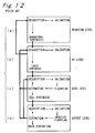
- FIG. 12 is a flowchart showing an example of the conventional VLSI design method according to a top-down approach (this example referred to as "prior art" hereinafter).
- the designer In designing a VLSI, the designer firstly analyzes given design constraints, thereafter explores the architecture candidates (implementation approach), chooses the most promising one and then describes the chosen architecture by means of a hardware description language (referred to as an "HDL” hereinafter) (this description referred to as a “behavioral description” hereinafter).
- the thus-obtained behavioral description is a design result at the behavior level. As shown in Fig. 12 (a), by subjecting this to a behavior level simulator or a verifier, the design at the behavior level is validated.
- RT level register transfer level
- RTL register transfer level
- the generation of the RTL description from the behavioral description is sometimes executed automatically by a behavioral synthesis tool.
- the generated RTL description is also a description in HDL.
- Fig. 12 (b) by subjecting this to an RT level simulator or the like, the design at the RT level is validated. In this stage, hypothetical wire lengths are assumed for interconnections.
- a net list (description of a logic circuit at a gate level) describing the object of design at the gate level from the RTL description by means of a logic synthesis tool.
- This net list is subjected to a logic simulator or the like as shown in Fig. 12 (c), by which the design at the gate level is validated and a floorplan is thereafter executed.
- the floorplan for the net list is to roughly place and wire blocks constituting the logic circuit at the gate level.
- the design at the gate level represented by the net list is estimated. That is, a chip area, a signal delay time, a power consumption and so forth are estimated by means of the information of the placement of blocks and the wiring between blocks constituting the logic circuit, and it is decided whether or not the design constraints are satisfied.
- the net list is corrected for the design change at the gate level so that the design constraints are satisfied, and the corrected net list is subjected to the validation, floorplan and estimation similar to the above.
- the processes of description change (design change by correcting the net list) ⁇ validation ⁇ floorplan ⁇ estimation are repeated at the gate level until the design at the gate level comes to satisfy the design constraints (see Fig. 12 (c)).
- the designer firstly returns to the RT level to make a description so as to change the design for the satisfaction of the design constraints.
- the designer further returns to the behavior level so as to correct the description data at the behavior level for a design change.
- the layout data is corrected in correspondence, and the corrected layout data is subjected to validation, floorplan and estimation.
- the processes of description change (design change by correcting the layout data) ⁇ validation ⁇ floorplan ⁇ estimation are repeated at the gate level until the design features represented by the chip area, delay time, power consumption and so forth become satisfied (see Fig. 12 (d)).
- the design constraints are not satisfied through the processes, there is sometimes a return to the higher level (gate level, RT level or behavior level) at need for a design change at the higher level.
- a mask pattern is generated from the layout data. Then, by means of a mask produced on the basis of this mask pattern, a VLSI is manufactured.
- the precise delay time and power consumption are estimated by means of the wiring information obtained through the layout design.
- the influence of the wiring on the delay time and the power consumption has been not so significant in the integrated circuit according to the conventional semiconductor manufacturing technique. Therefore, it has scarcely occurred to discover the fact that the design constraints are not satisfied at the layout level and the consequent return to the higher level for a design change, meaning that such a design change has not been a serious problem.
- the object of the present invention is to provide an integrated circuit design method and an integrated circuit design support apparatus for the method capable of eliminating the aforementioned problems by accurately estimating the delay time, power consumption and so forth of an object of design at higher levels of design.
- design features of the modules serving as the constituent elements of the object of design are estimated at each level corresponding to the abstraction level of design, the floorplan is executed at the behavior level or both the behavior level and the RT level by means of the design features, and design features of the object of design are estimated on the basis of the result of the floorplan. For this reason, it is allowed to estimate the signal delay time, power consumption and so forth taking the wiring delay and the wiring capacitance into consideration at the higher levels of design, i.e., in early stages of design, and therefore, it can be correctly decided whether or not the design satisfies the constraints.
- a shift from the design at the higher level to the design at the lower level will be made on the basis of this decision, and therefore, the possible occurrence of the requirement for a return from the lower level to the higher level for a design change can be prevented.
- a module of the object of design has a hierarchical structure
- a database apparatus for use in executing a design on a top-down approach for designing at a behavior level an integrated circuit which is an object of design with specified constraints thereby generating a behavior level description data of the object of design and successively generating description data at lower levels of abstraction from said behavior level description data, comprising:
- the floorplan oriented design described as above can be achieved by the integrated circuit design method according to the top-down approach. That is, even at the higher level such as the behavior level or the RT level, the floorplan can be executed by the design features of the module, thereby allowing the design features of the object of design to be estimated on the basis of the execution result.
- the database apparatus of the present invention a variety of modules which can be used as the constituent elements of the object of design are registered as parametrized models in the database, and therefore, the modules have high reusabilities, consequently allowing the efficiency of the designing work to be improved.
- an integrated circuit design support apparatus operated by a designer for executing a design on a top-down approach for designing at a behavior level an integrated circuit which is an object of design with specified constraints thereby generating a behavior level description data of the object of design and successively generating description data at lower levels of abstraction from said behavior level description data, comprising:
- the above integrated circuit design support apparatus of the present invention is provided with the aforementioned database apparatus as well as a means at the behavior level or both the behavior level and the RT level for correcting the description data of the object of design, executing the floorplan, estimating the design features and executing synthesis for the generation of the description data at the lower level, and therefore, the aforementioned estimation method or integrated circuit design method can be implemented by this integrated circuit design support apparatus.
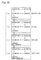
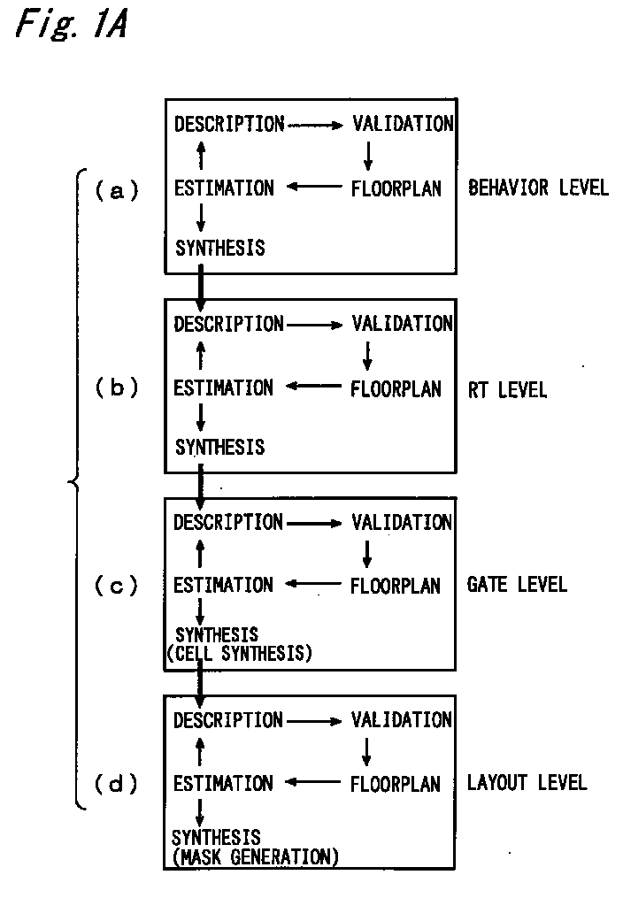
- Fig. 1A is a flowchart showing an integrated circuit design method of the present invention.
- the boxes indicated by the solid lines correspond to a behavior level, an RT level, a gate level and a layout level, representing the abstraction levels of design.
- Fig. 1B is a detailed flowchart showing a design process at one of the abstraction levels according to the present design method.
- the present design method is for designing a VLSI on a top-down approach similar to the prior art shown in Fig. 12, however, it differs from the prior art in that a floorplan and an estimation of the design based on it are executed both at the behavior level and the RT level.
- design features representing the design qualities of a chip area, a signal delay time, a power consumption and so forth (referred to as "design features" hereinafter) are calculated for the estimation of the design, and the processes of the description change of an object of design ⁇ validation ⁇ floorplan ⁇ estimation are repeated until no design change is required at each level.
- This placement allows the design features to be accurately estimated at a higher level as much as possible, thereby obviating the need for a return from the lower level to the higher level for a design change.
- An integrated circuit design support apparatus i.e., an integrated circuit design support apparatus for use in implementing the aforementioned integrated circuit design method will be described below.
- Fig. 2 is a schematic block diagram showing the hardware construction of the present integrated circuit design support apparatus.
- the hardware of the present integrated circuit design support apparatus is a computer system such as a work station constructed of a main body 100 having a CPU 106 and a memory 108, a hard disk drive 102, an input operation device 104 such as a keyboard and a mouse pointer and a display device 110 such as a CRT display. Then, the CPU 106 executes a specified program stored in the memory 108, so that a variety of functions for supporting the design of an integrated circuit on the top-down approach are realized.
- Fig. 3 is a functional block diagram schematically showing the construction of the present integrated circuit design support apparatus.
- the present integrated circuit design support apparatus is constructed of a DB storage 11 which stores therein a database based on FHM (Flexible Hardware Model) as described later, a database administrator system (referred to as a "DBMS" hereinafter) 12 for the FHM-DB, an operation unit 14, an input edition unit 16, a description storage 18 which stores therein description data obtained by describing the object of design at each level, a validation unit 22, a floorplanner 24, an estimation unit 26, a synthesis unit 28 and a display unit 20.
- the operation unit 14 and the display unit 20 correspond respectively to the input operation device 104 and the display device 110 shown in Fig. 2, and the DB storage 11 and the description storage 18 are provided by the hard disk drive 102.
- the other constituent elements shown in the functional block diagram of Fig. 3 are provided by the specified program stored in the memory 108.
- the DB storage 11 in which the FHM-DB is stored and the DBMS 12 constitute a database system 10 for the integrated circuit design (described in detail later).
- the FHM-DB is registered a variety of modules which can be used as the constituent elements of the integrated circuit of the object of design, and the DBMS 12 provides functions for executing extraction of information relevant to the registered module, registration of a new module into the FHM-DB and so forth.
- the input edition unit 16 generates a description data for describing the object of design, stores the same into the description storage 18 and executes the edition processes of effecting a change, addition and so forth on the description data stored in the description storage 18 on the basis of an input operation at the operation unit 14 conducted by the designer.
- the description data to be an object of edition is description data at each abstraction level obtained in each step of the top-down design, i.e., data describing the object of design at the behavior level, RT level, gate level and layout level.
- the validation unit 22 validates the design at each of the aforementioned levels by using the aforementioned description data at each of the aforementioned levels.
- the validation unit 22 is provided with a simulator for executing a simulation of the behavior of the object of design at each of the aforementioned levels, a verifier for verifying the design results at each of the aforementioned levels represented by the description data through a mathematical analysis and so forth.
- the validation unit 22 further includes the function of executing DRC (Design Rule Checking) for the validation of the design at the layout level.
- DRC Design Rule Checking
- the floorplanner 24 executes placement and wiring between modules which are the constituent elements of the object of design at each of the aforementioned levels (execution of floorplan).
- the estimation unit 26 estimates the design features of the whole object of design by means of the design features of the modules which are the constituent elements of the object of design at each of the aforementioned levels and the information of the placement and wiring obtained by executing the floorplan at each of the aforementioned levels. This enables the estimation of the design at each of the aforementioned levels. According to the design features of the whole object of design and design constraints, it is decided whether or not a change is required in the current stage of design, i.e., whether or not a correction of the description data of the object of design is required at the level corresponding to the current stage (referred to as a "current level” hereinafter). This decision may be made by the estimation unit 26. Alternatively, it is acceptable to display an estimation result (estimation result of design) by the estimation unit 26 on the display unit 20 and let the designer decide whether or not the description data at the current level is to be corrected by referring to the result.
- the synthesis unit 28 generates description data at a level one level lower than the current level from the description data at the current level when it is decided that any correction of the description data at the current level (design change at the current level) is not required and then stores the data into the description storage 18.
- the synthesis unit 28 does not generate any description data at the lower level. In this case, the designer corrects the description data at the current level by means of the operation unit 14 and the input edition unit 16.
- the display unit 20 displays the estimation result of the design at each level as stated before as well as processing results at the input edition unit 16, validation unit 22, floorplanner 24 and synthesis unit 28, and the designer can execute the required operation of correction of the description data and so forth by referring to them.
- the database system 10 which comprises the DB storage 11 storing the FHM-DB and the DBMS 12 will be described next.
- Fig. 4 is a functional block diagram showing a detailed construction of this database system 10.
- the database (FHM-DB) of this database system 10 is stored a variety of modules which can be used as the constituent elements of the object of design as a model having the following features.
- the model having the above-mentioned features (1), (2) and (3) are referred to as FHM (Flexible Hardware Model) herein.
- FHM Flexible Hardware Model
- information representing an instance generating method referred to as an "instance generating information” hereinafter
- information representing a method of estimating design features referred to as a “feature estimating information” hereinafter
- DB storage 11 at each of the abstraction levels of the behavior level, RT level, gate level and layout level for each registered module. That is, in the FHM-DB are described at each of abstraction levels (every level) for each registered module a procedure for generating an instance by means of the parameter values of the module and the estimating method for estimating the design features by means of the parameter values of the module.
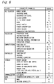
- the various models of FHM can be classified into several classes of a processor, a computational module, a control module, a storage module, a communication module, a wire module and a pad module as shown in Fig. 5. Then, as shown in Fig. 6, in regard to the parameters of FHM, some of them are common to all the classes, and the other parameters are inherent to the respective classes.
- the parameters whose usage is designated as "a” are those whose values are given to the model in instance generation and design feature estimation.
- the parameters whose usage is designated as "a/r” are those whose values are given to the model in instance generation and design feature estimation and are obtained as an estimation value.
- the parameters whose usage is designated as "r" are those whose values are obtained as an estimation value by design feature estimation or the like.
- the I/O port which corresponds to the module terminal, exists in all the modules. This is provided as an independent class and is made to have, for example, parameters as shown in Fig. 7 as its own attribute. That is, the class of I/O port has information relevant to the module terminal in the form of parameters.
- no hierarchical classification corresponding to each design level is performed, and parameters required at each design level (behavior level to layout level) are enumerated. For this reason, among the parameters enumerated herein are included those which are not used from the viewpoint of each level.
- the database administrator (DBMS) 12 is constructed of an input unit 52, a controller 54, an instantiation unit 58, a design feature estimation unit 60 and an output unit 56 as shown in Fig. 4, and this operates under the control of the controller 54 on the basis of instructions given to the DBMS 12.
- an instruction of newly registering a module defined by the designer (the module referred to as a "user definition module” hereinafter) is given to the DBMS 12, the input unit 52 is activated by the controller 54. Then, information relevant to the user definition module is inputted by the input unit 52 and stored into the DB storage 11, so that the user definition module is registered.
- the design feature estimation unit 60 when an instruction of estimating the design features of a register file which is a module at the RT level is given together with parameter values to the DBMS 12, the design feature estimation unit 60 is activated by the controller 54. Then, the design feature estimation unit 60 refers to feature estimation information at the RT level of the register file and estimates the design features representing the delay time, area, power consumption and so forth of the register file at the RT level by means of the information and the parameters given with the aforementioned instruction. For example, a hardware size (area or gate count) S in the case of the register file is estimated according to the following equation with a bit width B and a word count W used as parameters.
- the design features thus estimated by the design feature estimation unit 60 are outputted from the DBMS 12 by the output unit 56.
- the instantiation unit 58 when an instruction of generating an instance of the processor at the behavior level is given with parameter values to the DBMS 12, the instantiation unit 58 is activated by the controller 54. Then, the instantiation unit 58 refers to the information (instance generating information) in the FHM-DB representing the procedure of generating the instance of the processor module at the behavior level and generates the instance of the processor at the behavior level by means of the instance generating information and the parameter values given with the aforementioned instruction. Data representing the generated instance, i.e., data describing the processor module implemented by the aforementioned parameter values at the behavior level is outputted from the DBMS 12 by the output unit 56.
- the design feature estimation unit 60 refers to the feature estimation information of the processor module at the behavior level and also estimates the design features (area, execution cycles etc.) of the processor module implemented as the instance based on the information. Therefore, when the instruction of the instance generation described as above is issued, in addition to the data describing the processor implemented as the instance of the design at the behavior level, information representing the design features of the implemented processor is also obtained from the DBMS 12.
- Design Feature (Area, Delay Time, Execution Cycles, Power Consumption, ...)
- Area (Alb, Atyp, Aub)
- Delay Time (Dlb, Dtyp, Dub)
- the "delay time” and the "execution cycle” denote the performance of the module that is the object of estimation.
- the design feature estimation unit 60 estimates one or both of a range defined by the aforementioned lower bound (e.g., Alb) and the upper bound (e.g., Aub), and the typical value (e.g., Atyp).
- the typical value can be used as a reference in the design, which normally reflects a default implementation of the module.
- the design feature estimation unit 60 executes the estimation so that the aforementioned range of the design features is wide at the higher level and the aforementioned range of the design features is narrow at the lower level. Accordingly, in the stage of instance generation at the layout level, or the lowest level, the design features are estimated most accurately.
- the design features are estimated according to a procedure comprised of the following steps 1 through 3 (it is assumed that the user definition module is denoted by M in the following steps).
- the design features of this user definition module will be able to be estimated without executing the aforementioned procedure in the subsequent stages.
- the designer firstly analyzes the aforementioned design constraints, thereafter selects any one of the candidates for the aforementioned two implementation approaches and executes a design at the behavior level for the implementation of the object of design by the selected approach.
- the following statement is made on the assumption that the designer firstly adopts the Approach 1.
- the designer draws a data flow graph as shown in Fig. 8A representing the construction of the object of design at the behavior level according to the Approach 1 and describes this data flow graph by means of a specified hardware description language (HDL).
- HDL hardware description language
- This description data which is obtained by describing the object of design at the behavior level, can be considered as a design result at the behavior level.
- this design requires four multipliers and three adders. There is further required a controller for controlling the operations of these multipliers and adders. Therefore, instances of the modules of the multiplier, adder and controller are generated by the DBMS 12 in the description at the behavior level, and the description of the object of design is constituted by these instances. In this instance generating stage, the bit widths of the multiplier and the adder are given as the parameter values to the DBMS 12. Further, in this stage, the following information can be obtained as design features of the multiplier, adder and controller.
- the design result at the behavior level is validated by the validation unit 22 by means of this description data (step S12 in Fig. 1B).
- the validation unit 22 executes a functional validation by subjecting the description data at the behavior level to the behavior level simulator or the verifier.
- a floorplan is executed at the behavior level by the floorplanner 24 (step S16 in Fig. 1B). That is, the floorplanner 24 executes the placement of the modules (instances) implemented at the behavior level and wiring between those modules of the aforementioned multipliers, adders and controller on the basis of the description data at the behavior level. By this operation, a floorplan result as shown in Fig. 9A is obtained (note that the wiring between the modules is not shown). In executing the floorplan, information relevant to the terminals of the modules of the aforementioned multipliers, adders and controller are required for the wiring between the modules. Since the terminals of all the modules are modeled as I/O ports as stated before (see Fig.
- the DBMS 12 extracts the information of the terminal positions and so forth as the parameters of the I/O ports of the modules of the aforementioned multipliers, adders and controller in addition to the areas of the modules (step S14 in Fig. 1B), and these pieces of information are used.
- Fig. 10 shows a state in which wiring is being carried out according to the floorplan executed by means of these pieces of information.
- the estimation unit 26 estimates the design features of the object of design on the basis of the execution result of the floorplan (step S18 in Fig. 1B) and decides whether or not the design result satisfies the aforementioned design constraints on the basis of the estimation result (step S20).
- the design constraints are given as the conditions of the operating frequency, operation time and circuit scale, and therefore, the estimation unit 26 estimates the operating frequency, operation time and circuit scale of the object of design by means of the delay time and circuit scale relevant to the conditions of the design constraints among the design features of each module, or the constituent elements of the object of design at the behavior level.
- the design features of a module required for the estimation of the design are the circuit scale and the delay time of the module and they are obtained in the instance generating stage.
- the design feature estimation unit 60 in the DBMS 12 obtains the design features by referring to the feature estimation information of the module.
- the estimation result of the design at the behavior level as described above is displayed on the display unit 20, and the designer changes the design at the behavior level by referring to this.
- the validation and floorplan are executed similar to the case of the original description data (the case of Approach 1) (see Fig. 1A (a) and step S16 in Fig. 1B).
- the result of the floorplan is as shown in Fig. 9B (note that the wires between the modules are not shown).
- the design features of the object of design are estimated by the estimation unit 26 on the basis of the floorplan result (Step S18 in Fig. 1B), and it is decided whether or not the design result satisfies the aforementioned design constraints on the basis of the estimation result (step S20).
- the operating frequency, operation time and circuit scale of the object of design are estimated by means of the delay time and circuit scale relevant to the conditions of the design constraints among the design features of each module, or the constituent elements of the object of design at the behavior level, with the wire lengths obtained by the floorplan taken into consideration.
- the operation time of the object of design is estimated by means of the delay times of the product-sum operation unit and the register which are the constituent elements, with a wiring delay based on the wire lengths obtained through the floorplan taken into consideration. Assuming now that the delay time due to the wiring is 1.05 [ns], the delay times of the product-sum operation unit, register and controller are 61.1 to 92.2 [ns], 4.9 [ns] and 0.7 [ns], respectively, as stated before, and then a delay time of not greater than 100 [ns] results even when the delay time of the wiring is added to the sum of the delay time of the constituent elements of the object of design.
- step S20 in Fig. 1B When the design constraints at the behavior level are satisfied as described above, it is decided that no further correction of the description data at the behavior level is required (step S20 in Fig. 1B).
- the synthesis unit 28 On the basis of this decision, the synthesis unit 28 generates description data at the RT level from the description data at the behavior level by means of the behavioral synthesis tool (step S24 in Fig. 1B).
- the DBMS 12 generates the instances at the RT level of the modules of the product-sum operation unit, register and controller which are the constituent elements of the object of design, and the object of design is described by using those instances.
- the FHM-DB are described procedure for instance generation and so forth at every abstraction level for each registered module (see Fig. 4).
- the description at the RT level corresponding to each module at the behavior level can be easily obtained.
- a new parameter e.g., a parameter designating the algorithm of the adder in the product-sum operation unit
- the parameter is given by the designer.
- the algorithm may be automatically selected by the behavioral synthesis tool.
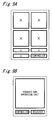
- Fig. 11A is a block diagram showing this design result, where the product-sum operation unit has a hierarchical structure.
- the design result becomes as shown in Fig. 11B.
- the design features of the module of the product-sum operation unit which is the constituent element of the object of design can he obtained by giving the bit width and the algorithm of the adder as parameters to the DBMS 12.
- the design result at the RT level is validated by the validation unit 22 by means of this description data (step S12 in Fig. 1B).
- the validation unit 22 executes functional validation by subjecting the description data at the RT level to the simulator or verifier at the RT level.
- a floorplan at the RT level is executed by the floorplanner 24 (step S16 in Fig. 1B). That is, the floorplanner 24 executes the placement of the modules (i.e., instances) of the multiplier, adder (whose algorithm is "ripple carry") and register which are the constituent elements of the object of design shown in Fig. 11B implemented at the RT level, and wiring between the modules, on the basis of the description data at the RT level.
- the DBMS 12 extracts information of the terminal positions which serve as parameters of the I/O ports of the modules and so forth in addition to the areas of the modules (step S14 in Fig. 1B), and these pieces of information are used for the floorplan.
- the estimation unit 26 estimates the design features of the object of design on the basis of the execution result of the floorplan to decide whether or not a design change at the RT level is required (step S18 in Fig. 1B).
- the operating frequency, operation time and circuit scale of the object of design are estimated by means of the delay time and circuit scale relevant to the conditions of the design constraints among the design features of the modules, or the constituent elements of the object of design at the RT level, with the wire lengths obtained through the floorplan taken into consideration.
- the fact that the design constraints are satisfied have been already discovered in the estimation of the design at the behavior level, and therefore, the operating frequency, operation time and circuit scale of the object of design estimated at the RT level satisfy the design constraints.
- These estimation values are displayed as estimation results at the RT level on the display unit 20, and the designer decides whether or not a design change at the RT level is required by referring to them (step S20 in Fig. 1B).
- the operation time and so forth are considered to have a small margin with respect to the design constraints. Therefore, the designer decides that a design change at the RT level is required and then corrects the description data at the RT level in an attempt at improving the performance (step S22 in Fig. 1B).
- the designer designates a "carry look-ahead" as an adder algorithm to generate an instance for the product-sum operation unit and then corrects the description data at the RT level so that this instance becomes a constituent element of the object of design. Then, in this instance generating stage, the following information is obtained as design features of the product-sum operation unit from the DBMS 12.
- the estimation unit 26 estimates the design features of the object of design on the basis of this floorplan result, and it is decided whether or not a further design change at the RT level is required (step S20 in Fig. 1B).
- the design features of the object of design as well as the operating frequency and operation time of the object of design estimated on the design features are displayed on the display unit 20, and the designer decides whether or not a design change at the RT level is required by referring to them.
- the design constraints are satisfied and the performance is improved (refer to the delay time of the aforementioned product-sum operation unit), and therefore, it is decided that no design change at the RT level is required.
- the synthesis unit 28 On the basis of this decision, the synthesis unit 28 generates description data (net list) at the gate level from the description data at the RT level by means of a logical synthesis tool (step S24 in Fig. 1B).
- the subsequent design procedure i.e., the design procedure at the gate level and the layout level is similar to that of the prior art design method (Fig. 12).
- the design result satisfies the design constraints at the higher level (behavior level) according to the design method shown in Fig. 1A, and therefore, the design results at the lower levels surely satisfy the design constraints.
- This arrangement prevents a time required for the completion of the design from being prolonged and becomes able to cope with an integrated circuit design in the deep submicron era.
- the design features can be obtained in the form of a range as stated before (see the expressions (2) through (5)). Therefore, even when the design constraints are not satisfied in the design at the higher level, it is possible that the design constraints be finally satisfied depending on the manner of design at the lower level so long as a portion satisfying the design constraints is included in the range of the design features.
- the design constraints are given as the conditions of the hardware cost (circuit scale) and the performance (operation time and operating frequency) in the above-mentioned example of design, it is often the case where the condition of the power consumption is included in the design constraints.
- the power consumption of the object of design is estimated at the estimation step at each design level. According to the present design method, even at the higher level of the behavior level or the RT level, the wiring capacitance between the modules can be taken into consideration on the basis of the result of the floorplan in the preceding step, in this estimation. With this arrangement, the power consumption of the object of design can be accurately estimated even at the higher level, and this eliminates the requirement of the return from the lower level to the higher level for a design change even when the condition of the power consumption is included in the design constraints.
Landscapes
- Engineering & Computer Science (AREA)
- Computer Hardware Design (AREA)
- Physics & Mathematics (AREA)
- Theoretical Computer Science (AREA)
- Evolutionary Computation (AREA)
- Geometry (AREA)
- General Engineering & Computer Science (AREA)
- General Physics & Mathematics (AREA)
- Design And Manufacture Of Integrated Circuits (AREA)
Abstract
Description
Delay time: 6.19 to 57.4 [ns]
Delay time: 54.97 [ns]
Circuit scale: 3065 to 3364 [gates]
Delay time: 61.1 to 92.2 [ns]
Delay time: 4.9 [ns]
Delay time of 0.7 [ns]
Claims (19)
- An estimation method of an integrated circuit design on a top-down approach for designing at a behavior level an integrated circuit which is an object of design with specified constraints thereby generating a behavior level description data (18) of the object of design and successively generating a description data (18) corresponding to lower levels of abstraction from said behavior level description data (18), said method comprising the steps of:preparing a database (11) wherein a variety of modules capable of being used as constituent elements of the object of design are registered as parametrized models, and instance generating information representing a procedure for generating (58) an instance which is a module implemented by giving a parameter value to each of the various modules and feature estimation information representing a method of estimating (60) specified design features representing the features of the various modules are stored every abstraction level of said design on the top-down approach for the various modules;generating (S10) a behavior level description data (18) by generating instances by means of the instance generating information and the parameter values of the modules registered in said database (11) and by describing at the behavior level the object of design with said instances used as constituent elements;extracting (S14;12) from said database (11) the feature estimation information of the modules described as the constituent elements of the object of design in said behavior level description data (18) and estimating (S14;60) design features of the modules by means of said feature estimation information and said parameter values of the modules;executing (S16;24) a floorplan corresponding to said behavior level description data (18) on the basis of the design features of said modules; andestimating (S18;26) design features representing features of the design at the behavior level corresponding to said behavior level description data (18) on the basis of a result of said floorplan.
- An estimation method of an integrated circuit design on a top-down approach for designing at a behavior level an integrated circuit which is an object of design with specified constraints thereby generating a behavior level description data (18) of the object of design and successively generating description data (18) corresponding to lower levels of abstraction from said behavior level description data (18), said method comprising the steps of:preparing a database (11) wherein a variety of modules capable of being used as constituent elements of the object of design are registered as parametrized models, and instance generating information representing a procedure for generating (58) an instance which is a module implemented by giving a parameter value to each of the various modules and feature estimation information representing a method of estimating (60) specified design features representing the features of the various modules are stored every abstraction level of said design on the top-down approach for the various modules;generating (S10;S24;28) a RTL description data which is a description data of the object of design at a register transfer level from said behavior level description data (18) by means of the instance generating information at the register transfer level stored in said database (11);extracting (S14;12) from said database (11) the feature estimation information of the modules described as the constituent elements of the object of design in said RTL description data (18) and estimating design features of the modules by means of said feature estimation information and said parameter values of the modules;executing (S16;24) a floorplan corresponding to said RTL description data (18) on the basis of the design features of said modules; andestimating (S18;26) design features representing features of the design at the register transfer level corresponding to said RTL description data (18) on the basis of a result of said floorplan.
- An integrated circuit design method on a top-down approach for designing at a behavior level an integrated circuit which is an object of design with specified constraints thereby generating a behavior level description data (18) of the object of design and successively generating a description data (18) corresponding to lower levels of abstraction from said behavior level description data (18), said method comprising:a first step of preparing a database (11) wherein a variety of modules capable of being used as constituent elements of the object of design are registered as parametrized models, and instance generating information representing a procedure for generating (58) an instance which is a module implemented by giving a parameter value to each of the various modules and feature estimation information representing a method of estimating (60) specified design features representing the features of the various modules are stored every abstraction level of said design on the top-down approach for the various modules;a second step (S10) of generating a behavior level description data (18) by generating (58) instances by means of the instance generating information and the parameter values of the modules registered in said database (11) and by describing at the behavior level the object of design with said instances used as constituent elements;a third step (S14) of extracting from said database (11) the feature estimation information of the modules described as the constituent elements of the object of design in said behavior level description data (18) and estimating (S14;60) design features of the modules by means of said feature estimation information and said parameter values of the modules;a fourth step (S16;24) of executing a floorplan corresponding to said behavior level description data (18) on the basis of the design features estimated in the third step;a fifth step (S18;26) of estimating design features representing features of the design at the behavior level represented by said behavior level description data (18) on the basis of an result of the floorplan in the fourth step;a sixth step (S20) of deciding whether or not a design change at the behavior level is required on the basis of the design features estimated in the fifth step and the constraints of the object of design;a seventh step (S22) of obtaining a new behavior level description data by changing said behavior level description data (18) when it is decided that a design change at the behavior level is required in the sixth step; andan eighth step (S24) of generating an RTL description data (18) which is a description data of the object of design at a register transfer level from said behavior level description data (18) which is an object of the decision in the sixth step by means of said instance generating information at the register transfer level stored in said database (11) when it is decided that no design change at the behavior level is required in the sixth step,
whereby the processes of obtaining a new behavior level description data in the seventh step (S24) and successively executing the third step (S14), fourth step (S16), fifth step (S18) and sixth step (S20) on the new behavior level description data (18) are repeated while it is decided that a design change at the behavior level is required in the sixth step (S20). - An integrated circuit design method as claimed in Claim 3, further comprising:a ninth step (S14) of extracting the feature estimation information of the modules described as the constituent elements of the object of design in said RTL description data (18) and estimating (S14;60) the design features of the modules by means of said feature estimation information and said parameter values of the modules;a tenth step (S16;24) of executing a floorplan corresponding to said RTL description data (18) on the basis of the design features estimated in the ninth step (S14);a eleventh step (S18;26) of estimating design features representing the design features at the register transfer level represented by said RTL description data (18) on the basis of a result of the floorplan in the tenth step (S16);a twelfth step (S20) of deciding whether or not a design change at the register transfer level is required on the basis of the design features estimated in the eleventh step (S18) and the constraints of the object of design;a thirteenth (S22) step of obtaining a new RTL description data of the object of design by changing said RTL description data (18) when it is decided that a design change at the register transfer level is required in the twelfth step (S20); anda fourteenth (S24) step of generating a net list which is a description data of the object of design at a gate level from said RTL description data (18) which is an object of the decision in the twelfth step (S20) by means of said instance generating information at the gate level stored in said database (11) when it is decided that no design change at the register transfer level is required in the twelfth step (S20),
whereby the processes of obtaining the new RTL description (18) in the thirteenth step (S13) and successively executing the ninth step (S14), tenth step (S16), eleventh step (S18) and twelfth step (S20) on the new RTL description data (18) are repeated while it is decided that a design change at the register transfer level is required in the twelfth step (S20). - An estimation method as claimed in Claim 1, whereina module having a hierarchical structure is registered in said database (11), anda floorplan is executed (24) on the basis of information of interconnection between submodules constituting said module and design features of the module having said hierarchical structure are estimated (26) by means of a result of said floorplan and design features of the submodules in estimating the design features of said module having said hierarchical structure.
- An integrated circuit design method as claimed in Claim 3, whereina module having a hierarchical structure is registered in said database (11), anda floorplan is executed (24) on the basis of information of interconnection between submodules constituting said module and design features of the module having said hierarchical structure are estimated (26) by means of a result of said floorplan and design features of the submodules in estimating the design features of said module having said hierarchical structure.
- An integrated circuit design method as claimed in Claim 3, whereinit is decided in said sixth step (S20) whether or not a design change at the behavior level is required depending on whether or not the design features estimated in said fifth step (S18) satisfy the design constraints of the object of design.
- An integrated circuit design method as claimed in Claim 4, whereinit is decided in said twelfth step (S20) whether or not a design change at the register transfer level is required depending on whether or not the design features estimated in said eleventh step (S18) are higher than a specified level.
- An integrated circuit design method as claimed in Claim 3 or 4, whereinthe design features estimated in said third, fifth, ninth and eleventh steps (S14,S18) include values representing an area and a performance or a range of the values.
- An integrated circuit design method as claimed in Claim 9, whereinthe design features estimated in said third and ninth steps (S14) include information representing positions and types of terminals of the modules which are the constituent elements of the object of design, andthe floorplan is executed in said fourth and tenth steps (S16) on the basis of the information representing the area and the positions and types of the terminals represented by the design features of the modules which are the constituent elements of the object of design.
- An integrated circuit design method as claimed in Claim 9, wherein the design features estimated in said third, fifth, ninth and eleventh steps (S14,S18) include a value representing a power consumption or a range of the value.
- An integrated circuit design method as claimed in Claim 10, whereinthe design features estimated in said third, fifth, ninth and eleventh steps (S14,S18) include a value representing a power consumption or a range of the value.
- A database apparatus for use in executing a design on a top-down approach for designing at a behavior level an integrated circuit which is an object of design with specified constraints thereby generating a behavior level description data (18) of the object of design and successively generating description data (18) at lower levels of abstraction from said behavior level description data (18), said apparatus comprising:a storage means (11) for storing therein a database in which a variety of modules capable of being used as constituent elements of the object of design are registered as parametrized models, and instance generating information representing a procedure for generating an instance which is a module implemented by giving a parameter value to each of the various modules and feature estimation information representing a method of estimating specified design features representing the features of the various modules are stored every abstraction level of said design on the top-down approach for the various modules;an instance generating means (58) for extracting an instance generating information of any of modules registered at an abstraction level in said database and for generating an instance for said module by means of said instance generating information and parameter values of said module, when said module and said abstraction level are designated and said parameter values are given; anda module feature estimating means (60) for extracting a feature estimation information of any of modules registered at an abstraction level in said database and for estimating design features for said module by means of said feature estimation information and parameter values of said module, when said module and said abstraction level are designated and said parameter values are given.
- An integrated circuit design support apparatus operated by a designer for executing a design on a top-down approach for designing at a behavior level an integrated circuit which is an object of design with specified constraints thereby generating a behavior level description data (18) of the object of design and successively generating description data (18) at lower levels of abstraction from said behavior level description data (18), said design support apparatus comprising:said database apparatus (10) claimed in Claim 13;a description data generating and editing means (16) for generating and editing said behavior level description data by generating instances by means of said instance generating information and by describing at the behavior level the object of design with said instances used as constituent elements on the basis of an input operation conducted by said designer;a floorplan executing means (24) for obtaining design features of modules described as constituent elements of the object of design in said behavior level description data (18) by said module feature estimating means (60) by means of parameter values of the modules and executing a floorplan corresponding to said behavior level description data on the basis of said design features;a design feature estimating means (26) for estimating design features representing features of the design at the behavior level corresponding to said behavior level description data (18) on the basis of a result of said floorplan; anda behavioral synthesis means (28) for generating an RTL description data (18) describing the object of design at a register transfer level from said behavior level description data (18) describing the object of design at the behavior level by means of said instance generating information at the register transfer level stored in said database.
- An integrated circuit design support apparatus as claimed in Claim 14, whereinsaid description data generating and editing means (16) also edits said RTL description data (18) generated by said behavioral synthesis means (28) on the basis of an input operation conducted by said designer,said floorplan executing means (24) acquires design features by said module feature estimating means (60) also in connection with said RTL description data (18) and executes the floorplan corresponding to said RTL description data (18) on the basis of the information of said design features, andsaid design feature estimating means (26) also estimates design features representing features of the design at the register transfer level on the basis of a result of the floorplan corresponding to said RTL description data (18).
- An integrated circuit design support apparatus as claimed in Claim 14 or 15, whereinsaid design features estimated by said module feature estimating means (60) and said design feature estimating means (26) include values representing an area and a performance or a range of the values.
- An integrated circuit design support apparatus as claimed in Claim 16, whereinsaid design features estimated by said module feature estimating means (60) include information representing positions and types of terminals of the modules which are the constituent elements of the object of design, andsaid floorplan executing means (24) executes the floorplan on the basis of said area and said information representing positions and types of terminals which are represented by the design features of the modules which are the constituent elements of the object of design.
- An integrated circuit design support apparatus as claimed in Claim 16, whereinsaid design features estimated by said module feature estimating means (60) and said design feature estimating means (26) include a value representing a power consumption or a range of the value.
- An integrated circuit design support apparatus as claimed in Claim 17, whereinsaid design features estimated by said module feature estimating means (60) and said design feature estimating means (26) include a value representing a power consumption or a range of the value.
Applications Claiming Priority (3)
| Application Number | Priority Date | Filing Date | Title |
|---|---|---|---|
| JP8333539A JP2954894B2 (en) | 1996-12-13 | 1996-12-13 | Integrated circuit design method, database device for integrated circuit design, and integrated circuit design support device |
| JP33353996 | 1996-12-13 | ||
| JP333539/96 | 1996-12-13 |
Publications (2)
| Publication Number | Publication Date |
|---|---|
| EP0848342A2 true EP0848342A2 (en) | 1998-06-17 |
| EP0848342A3 EP0848342A3 (en) | 2001-01-10 |
Family
ID=18267185
Family Applications (1)
| Application Number | Title | Priority Date | Filing Date |
|---|---|---|---|
| EP97121676A Ceased EP0848342A3 (en) | 1996-12-13 | 1997-12-09 | Intergrated circuit design method, database apparatus for designing integrated circuit and integrated circuit design support apparatus |
Country Status (5)
| Country | Link |
|---|---|
| US (1) | US6026228A (en) |
| EP (1) | EP0848342A3 (en) |
| JP (1) | JP2954894B2 (en) |
| KR (1) | KR100281977B1 (en) |
| TW (1) | TW432304B (en) |
Cited By (6)
| Publication number | Priority date | Publication date | Assignee | Title |
|---|---|---|---|---|
| US6467074B1 (en) | 2000-03-21 | 2002-10-15 | Ammocore Technology, Inc. | Integrated circuit architecture with standard blocks |
| EP1736905A2 (en) * | 2005-06-21 | 2006-12-27 | Nvidia Corporation | Building integrated circuits using logical units |
| US7363610B2 (en) | 2005-06-21 | 2008-04-22 | Nvidia Corporation | Building integrated circuits using a common database |
| US7483823B2 (en) | 2005-06-21 | 2009-01-27 | Nvidia Corporation | Building integrated circuits using logical units |
| US7735050B2 (en) | 2006-02-09 | 2010-06-08 | Henry Yu | Managing and controlling the use of hardware resources on integrated circuits |
| US7831938B2 (en) | 2000-12-21 | 2010-11-09 | Mentor Graphics Corporation | Interactive interface resource allocation in a behavioral synthesis tool |
Families Citing this family (42)
| Publication number | Priority date | Publication date | Assignee | Title |
|---|---|---|---|---|
| US6169968B1 (en) * | 1997-07-09 | 2001-01-02 | Matsushita Electric Industrial Co., Ltd. | Apparatus and method for estimating performance integrated circuit |
| US6260182B1 (en) * | 1998-03-27 | 2001-07-10 | Xilinx, Inc. | Method for specifying routing in a logic module by direct module communication |
| US6216258B1 (en) | 1998-03-27 | 2001-04-10 | Xilinx, Inc. | FPGA modules parameterized by expressions |
| US6243851B1 (en) | 1998-03-27 | 2001-06-05 | Xilinx, Inc. | Heterogeneous method for determining module placement in FPGAs |
| US6292925B1 (en) | 1998-03-27 | 2001-09-18 | Xilinx, Inc. | Context-sensitive self implementing modules |
| US6430732B1 (en) | 1998-03-27 | 2002-08-06 | Xilinx, Inc. | Method for structured layout in a hardware description language |
| US6237129B1 (en) | 1998-03-27 | 2001-05-22 | Xilinx, Inc. | Method for constraining circuit element positions in structured layouts |
| US6199031B1 (en) * | 1998-08-31 | 2001-03-06 | Vlsi Technology, Inc. | HDL simulation interface for testing and verifying an ASIC model |
| JP3562975B2 (en) * | 1998-09-29 | 2004-09-08 | 株式会社東芝 | Integrated circuit design method and integrated circuit design device |
| JP2000123061A (en) | 1998-10-16 | 2000-04-28 | Matsushita Electric Ind Co Ltd | Database and method for designing integrated circuit device |
| US6233724B1 (en) | 1998-10-30 | 2001-05-15 | Micron Technology, Inc. | Circuit synthesis time budgeting based upon wireload information |
| US6226777B1 (en) * | 1998-11-25 | 2001-05-01 | Agilent Technologies, Inc. | Method and system for improving the performance of a circuit design verification tool |
| US6591402B1 (en) | 1999-03-19 | 2003-07-08 | Moscape, Inc. | System and method for performing assertion-based analysis of circuit designs |
| JP3250542B2 (en) | 1999-03-23 | 2002-01-28 | 日本電気株式会社 | LSI design method |
| US6505328B1 (en) * | 1999-04-27 | 2003-01-07 | Magma Design Automation, Inc. | Method for storing multiple levels of design data in a common database |
| US6298472B1 (en) * | 1999-05-07 | 2001-10-02 | Chameleon Systems, Inc. | Behavioral silicon construct architecture and mapping |
| US6581029B1 (en) * | 1999-05-11 | 2003-06-17 | International Business Machines Corporation | Method and system for optimizing execution of a collection of related module sequences by eliminating redundant modules |
| US6671857B1 (en) * | 1999-08-18 | 2003-12-30 | Matsushita Electric Industrial Co., Ltd. | Method of designing integrated circuit device using common parameter at different design levels, and database thereof |
| JP2001067384A (en) * | 1999-08-26 | 2001-03-16 | Matsushita Electric Ind Co Ltd | Database for designing integrated circuit device and method for designing the device |
| US6397341B1 (en) * | 1999-08-27 | 2002-05-28 | Synopsys, Inc. | Method for improving the speed of behavioral synthesis links to logic synthesis |
| US7062425B1 (en) * | 1999-09-30 | 2006-06-13 | Cypress Semiconductor Corp. | Method and apparatus for automated enumeration, simulation, identification and/or irradiation of device attributes |
| US6804810B1 (en) * | 2000-02-21 | 2004-10-12 | Hewlett-Packard Development Company, L.P. | Resistance and capacitance estimation |
| JP2002163324A (en) * | 2000-11-28 | 2002-06-07 | Hitachi Ltd | Delay time calculating method and method for designing semiconductor integrated circuit by using the same |
| JP2002318825A (en) * | 2001-04-20 | 2002-10-31 | Hitachi Ltd | Designing method for logic circuit |
| EP1402401A4 (en) | 2001-06-15 | 2007-10-03 | Cadence Design Systems Inc | Enhancing mergeability of datapaths and reducing datapath widths by rebalancing data flow topology |
| KR100429573B1 (en) * | 2001-12-24 | 2004-05-03 | 주식회사 하이닉스반도체 | Method for creating Register transfer level code |
| US20030120475A1 (en) * | 2001-12-26 | 2003-06-26 | Toshiba Tec Kabushiki Kaisha | Method of generating asic design database |
| JP3825328B2 (en) * | 2002-01-23 | 2006-09-27 | Necエレクトロニクス株式会社 | Processor synthesis apparatus, system LSI synthesis apparatus, processor synthesis method, system LSI synthesis method, and recording medium |
| JP2003316838A (en) * | 2002-04-19 | 2003-11-07 | Nec Electronics Corp | Design method for system lsi and storage medium with the method stored therein |
| JP4541783B2 (en) * | 2004-06-30 | 2010-09-08 | 富士通セミコンダクター株式会社 | Semiconductor integrated circuit design method, design apparatus, and logic design program |
| US20060156268A1 (en) * | 2005-01-13 | 2006-07-13 | Wen Kuei-Ann | Circuit design platform |
| KR100809684B1 (en) | 2005-08-22 | 2008-03-06 | 삼성전자주식회사 | verification apparatus for verify the power off effect on Register Transfer Level and modeling method for power off effect |
| JP5114877B2 (en) * | 2006-06-27 | 2013-01-09 | 富士通株式会社 | Design data creation method, design data creation device, and design data creation program |
| US8516418B2 (en) * | 2006-06-30 | 2013-08-20 | Oracle America, Inc. | Application of a relational database in integrated circuit design |
| US8595674B2 (en) | 2007-07-23 | 2013-11-26 | Synopsys, Inc. | Architectural physical synthesis |
| US8819608B2 (en) | 2007-07-23 | 2014-08-26 | Synopsys, Inc. | Architectural physical synthesis |
| US8307315B2 (en) | 2009-01-30 | 2012-11-06 | Synopsys, Inc. | Methods and apparatuses for circuit design and optimization |
| US8082530B1 (en) * | 2009-02-20 | 2011-12-20 | Xilinx, Inc. | Power estimation in high-level modeling systems |
| CN102708265B (en) * | 2012-06-12 | 2014-01-22 | 电子科技大学 | Direct and integrated design method of band-pass filters |
| KR102218200B1 (en) | 2014-03-06 | 2021-02-23 | 삼성전자주식회사 | System and method for RTL Auto-integration using spread-sheet and recording medium thereof |
| JP5839379B1 (en) * | 2015-02-12 | 2016-01-06 | アダプトIp株式会社 | IP automatic generation system |
| JP7081331B2 (en) * | 2018-06-22 | 2022-06-07 | 日本電気株式会社 | Circuit synthesizer, circuit synthesizer, and circuit synthesizer program |
Citations (1)
| Publication number | Priority date | Publication date | Assignee | Title |
|---|---|---|---|---|
| US5572436A (en) * | 1990-04-06 | 1996-11-05 | Lsi Logic Corporation | Method and system for creating and validating low level description of electronic design |
Family Cites Families (13)
| Publication number | Priority date | Publication date | Assignee | Title |
|---|---|---|---|---|
| US5557531A (en) * | 1990-04-06 | 1996-09-17 | Lsi Logic Corporation | Method and system for creating and validating low level structural description of electronic design from higher level, behavior-oriented description, including estimating power dissipation of physical implementation |
| US5544066A (en) * | 1990-04-06 | 1996-08-06 | Lsi Logic Corporation | Method and system for creating and validating low level description of electronic design from higher level, behavior-oriented description, including estimation and comparison of low-level design constraints |
| US5870308A (en) * | 1990-04-06 | 1999-02-09 | Lsi Logic Corporation | Method and system for creating and validating low-level description of electronic design |
| US5499192A (en) * | 1991-10-30 | 1996-03-12 | Xilinx, Inc. | Method for generating logic modules from a high level block diagram |
| DE69325770T2 (en) * | 1992-06-02 | 1999-11-18 | Hewlett Packard Co | METHOD FOR COMPUTER-BASED DESIGN FOR MULTI-LAYER CONNECTION TECHNOLOGIES |
| US5557532A (en) * | 1992-11-12 | 1996-09-17 | Vlsi Technology, Inc. | Parameterized generic compiler |
| US5566079A (en) * | 1992-11-12 | 1996-10-15 | Vlsi Technology, Inc. | Parameterized generic multiplier complier |
| US5487018A (en) * | 1993-08-13 | 1996-01-23 | Vlsi Technology, Inc. | Electronic design automation apparatus and method utilizing a physical information database |
| US5533148A (en) * | 1993-09-30 | 1996-07-02 | International Business Machines Corporation | Method for restructuring physical design images into hierarchical data models |
| US5953519A (en) * | 1995-06-12 | 1999-09-14 | Fura; David A. | Method and system for generating electronic hardware simulation models |
| US5764532A (en) * | 1995-07-05 | 1998-06-09 | International Business Machines Corporation | Automated method and system for designing an optimized integrated circuit |
| US5841663A (en) * | 1995-09-14 | 1998-11-24 | Vlsi Technology, Inc. | Apparatus and method for synthesizing integrated circuits using parameterized HDL modules |
| US5802349A (en) * | 1996-01-22 | 1998-09-01 | Motorola, Inc. | Method for generating an optimized integrated circuit cell library |
-
1996
- 1996-12-13 JP JP8333539A patent/JP2954894B2/en not_active Expired - Fee Related
-
1997
- 1997-12-05 TW TW086118367A patent/TW432304B/en not_active IP Right Cessation
- 1997-12-09 EP EP97121676A patent/EP0848342A3/en not_active Ceased
- 1997-12-10 KR KR1019970067401A patent/KR100281977B1/en not_active IP Right Cessation
- 1997-12-12 US US08/989,425 patent/US6026228A/en not_active Expired - Lifetime
Patent Citations (1)
| Publication number | Priority date | Publication date | Assignee | Title |
|---|---|---|---|---|
| US5572436A (en) * | 1990-04-06 | 1996-11-05 | Lsi Logic Corporation | Method and system for creating and validating low level description of electronic design |
Non-Patent Citations (5)
| Title |
|---|
| KUMAR T ET AL: "Hierarchical behavioral partitioning for multicomponent synthesis" PROCEEDINGS OF EURO-DAC: EUROPEAN DESIGN AUTOMATION CONFERENCE WITH EURO-VDL AND EXHIBITION,US,LOS ALAMITOS, IEEE COMP. SOC. PRESS, 1996, pages 212-217, XP002109792 ISBN: 0-8186-7573-X * |
| MEYER W.; CAMPOSANO R.: 'FAST HIERARCHICAL MULTI-LEVEL FAULT SIMULATION OF SEQUENTIAL CIRCUITS WITH SWITCH-LEVEL ACCURACY' PROCEEDINGS OF THE DESIGN AUTOMATION CONFERENCE vol. 30, 14 June 1993, NEW YORK, pages 515 - 519, XP000371358 * |
| SHACKLEFORD B ET AL: "SATSUKI: AN INTEGRATED PROCESSOR SYNTHESIS AND COMPILER GENERATION SYSTEM" IEICE TRANSACTIONS ON INFORMATION AND SYSTEMS,JP,INSTITUTE OF ELECTRONICS INFORMATION AND COMM. ENG. TOKYO, vol. E79-D, no. 10, 1 October 1996 (1996-10-01), pages 1373-1381, XP000635525 ISSN: 0916-8532 * |
| SHAHID KHAM: "RTL FLOORPLANNING SPEEDS DEEP-SUBMICRON DESIGN" COMPUTER DESIGN,US,PENNWELL PUBL. LITTLETON, MASSACHUSETTS, vol. 35, no. 2, 1 February 1996 (1996-02-01), pages 103-106, XP000555485 ISSN: 0010-4566 * |
| TUCK B: "RTL floorplanner predicts timing, power for deep-submicron ICs" COMPUTER DESIGN,PENNWELL PUBL. LITTLETON, MASSACHUSETTS,US, vol. 35, no. 4, March 1996 (1996-03), pages 56-57,59, XP002109793 ISSN: 0010-4566 * |
Cited By (10)
| Publication number | Priority date | Publication date | Assignee | Title |
|---|---|---|---|---|
| US6467074B1 (en) | 2000-03-21 | 2002-10-15 | Ammocore Technology, Inc. | Integrated circuit architecture with standard blocks |
| US7831938B2 (en) | 2000-12-21 | 2010-11-09 | Mentor Graphics Corporation | Interactive interface resource allocation in a behavioral synthesis tool |
| EP1736905A2 (en) * | 2005-06-21 | 2006-12-27 | Nvidia Corporation | Building integrated circuits using logical units |
| EP1736905A3 (en) * | 2005-06-21 | 2007-09-05 | Nvidia Corporation | Building integrated circuits using logical units |
| US7363610B2 (en) | 2005-06-21 | 2008-04-22 | Nvidia Corporation | Building integrated circuits using a common database |
| US7483823B2 (en) | 2005-06-21 | 2009-01-27 | Nvidia Corporation | Building integrated circuits using logical units |
| CN1885295B (en) * | 2005-06-21 | 2011-01-19 | 辉达公司 | Building integrated circuits using logical units |
| US7735050B2 (en) | 2006-02-09 | 2010-06-08 | Henry Yu | Managing and controlling the use of hardware resources on integrated circuits |
| US8726204B2 (en) | 2006-02-09 | 2014-05-13 | Mentor Graphics Corporation | Managing and controlling the use of hardware resources on integrated circuits |
| US9747398B2 (en) | 2006-02-09 | 2017-08-29 | Mentor Graphics Corporation | Managing and controlling the use of hardware resources on integrated circuits |
Also Published As
| Publication number | Publication date |
|---|---|
| TW432304B (en) | 2001-05-01 |
| JP2954894B2 (en) | 1999-09-27 |
| EP0848342A3 (en) | 2001-01-10 |
| JPH10171857A (en) | 1998-06-26 |
| KR19980063998A (en) | 1998-10-07 |
| US6026228A (en) | 2000-02-15 |
| KR100281977B1 (en) | 2001-02-15 |
Similar Documents
| Publication | Publication Date | Title |
|---|---|---|
| US6026228A (en) | Integrated circuit design method, database apparatus for designing integrated circuit and integrated circuit design support apparatus | |
| US5896300A (en) | Methods, apparatus and computer program products for performing post-layout verification of microelectronic circuits by filtering timing error bounds for layout critical nets | |
| US7571405B1 (en) | Electrical design rule checking expert traverser system | |
| US6272668B1 (en) | Method for cell swapping to improve pre-layout to post-layout timing | |
| US7020856B2 (en) | Method for verifying properties of a circuit model | |
| US6574779B2 (en) | Hierarchical layout method for integrated circuits | |
| US7225423B2 (en) | Method for automated design of integrated circuits with targeted quality objectives using dynamically generated building blocks | |
| US7937256B2 (en) | Systems and methods of efficient library characterization for integrated circuit cell libraries | |
| US7206731B2 (en) | Electromagnetic/circuit co-simulation and co-optimization with parametric layout components | |
| US8086978B2 (en) | Method and system for performing statistical leakage characterization, analysis, and modeling | |
| US6536023B1 (en) | Method and system for hierarchical metal-end, enclosure and exposure checking | |
| US7096447B1 (en) | Method and apparatus for efficiently locating and automatically correcting certain violations in a complex existing circuit layout | |
| US6539528B2 (en) | Methods, systems, and computer program products for designing an integrated circuit that use an information repository having circuit block layout information | |
| US20070245280A1 (en) | System and method for placement of soft macros | |
| US7373618B1 (en) | Method and system for selection and replacement of subcircuits in equivalence checking | |
| US7353490B2 (en) | Power network synthesizer for an integrated circuit design | |
| US7240311B2 (en) | Combinational equivalence checking methods and systems with internal don't cares | |
| US20040210861A1 (en) | System and method for optimizing exceptions | |
| US6931610B1 (en) | Method for rapid estimation of wire delays and capacitances based on placement of cells | |
| US7117465B2 (en) | Application of the retimed normal form to the formal equivalence verification of abstract RTL descriptions for pipelined designs | |
| CN116940929A (en) | Method, electronic device, computer-readable storage medium, and program product for simulating a circuit | |
| US7191412B1 (en) | Method and apparatus for processing a circuit description for logic simulation | |
| US6701496B1 (en) | Synthesis with automated placement information feedback | |
| US11727186B2 (en) | Automatic identification of hierarchical cells based on selected properties for layout verification | |
| WO2023080890A1 (en) | Automated cell black boxing for layout versus schematic |
Legal Events
| Date | Code | Title | Description |
|---|---|---|---|
| PUAI | Public reference made under article 153(3) epc to a published international application that has entered the european phase |
Free format text: ORIGINAL CODE: 0009012 |
|
| AK | Designated contracting states |
Kind code of ref document: A2 Designated state(s): DE FR GB |
|
| AX | Request for extension of the european patent |
Free format text: AL;LT;LV;MK;RO;SI |
|
| PUAL | Search report despatched |
Free format text: ORIGINAL CODE: 0009013 |
|
| AK | Designated contracting states |
Kind code of ref document: A3 Designated state(s): AT BE CH DE DK ES FI FR GB GR IE IT LI LU MC NL PT SE |
|
| AX | Request for extension of the european patent |
Free format text: AL;LT;LV;MK;RO;SI |
|
| 17P | Request for examination filed |
Effective date: 20010710 |
|
| AKX | Designation fees paid |
Free format text: DE FR GB |
|
| 17Q | First examination report despatched |
Effective date: 20050531 |
|
| STAA | Information on the status of an ep patent application or granted ep patent |
Free format text: STATUS: THE APPLICATION HAS BEEN REFUSED |
|
| 18R | Application refused |
Effective date: 20070809 |