EP0847024A2 - Fingerprint input apparatus - Google Patents
Fingerprint input apparatus Download PDFInfo
- Publication number
- EP0847024A2 EP0847024A2 EP97121472A EP97121472A EP0847024A2 EP 0847024 A2 EP0847024 A2 EP 0847024A2 EP 97121472 A EP97121472 A EP 97121472A EP 97121472 A EP97121472 A EP 97121472A EP 0847024 A2 EP0847024 A2 EP 0847024A2
- Authority
- EP
- European Patent Office
- Prior art keywords
- prism
- light
- fingerprint
- fingerprint collection
- collection surface
- Prior art date
- Legal status (The legal status is an assumption and is not a legal conclusion. Google has not performed a legal analysis and makes no representation as to the accuracy of the status listed.)
- Withdrawn
Links
Images


Classifications
-
- G—PHYSICS
- G06—COMPUTING; CALCULATING OR COUNTING
- G06V—IMAGE OR VIDEO RECOGNITION OR UNDERSTANDING
- G06V40/00—Recognition of biometric, human-related or animal-related patterns in image or video data
- G06V40/10—Human or animal bodies, e.g. vehicle occupants or pedestrians; Body parts, e.g. hands
- G06V40/12—Fingerprints or palmprints
- G06V40/13—Sensors therefor
- G06V40/1324—Sensors therefor by using geometrical optics, e.g. using prisms
Definitions
- the present invention relates to a fingerprint input apparatus for inputting fingerprints to register them or collate them with fingerprints already registered.
- fingerprint collation systems are especially used in the fields that require high degrees of security.
- An apparatus for inputting fingerprint images is a constituent element of such a fingerprint collation system.
- This fingerprint input apparatus includes an optical system as a constituent. The collation precision of the fingerprint collation system greatly depends on whether fingerprint images can be correctly input.
- the present invention has been made to solve this problem, and has as its object to provide a fingerprint input apparatus which can obtain high-quality fingerprint images.
- a fingerprint input apparatus comprising a prism placed such that a surface in one direction serves as a fingerprint collection surface, a light source for irradiating light on the fingerprint collection surface through the prism, a pinhole set in a path of light which is reflected by a pattern surface of a finger placed on the fingerprint collection surface and emerges from the prism, and an imaging plane on which the light emerging from the prism and passing through the pinhole is formed into an image, wherein when the prism is substituted by air, an optical fingerprint collection surface equivalent to the fingerprint collection surface is set to be substantially parallel to the imaging plane.
- light reflected by the pattern surface of the finger directly or indirectly placed on the fingerprint collection surface and emerging from the prism passes through the pinhole and is formed into an image on the imaging plane set to be almost parallel to the optical fingerprint collection surface of the prism.
- the imaging plane when the optical fingerprint collection surface has distortion with respect to the fingerprint collection surface, the imaging plane is rotated through a predetermined angle. According to this aspect, distortion caused on the optical fingerprint collection surface can be reduced by rotating the imaging plane almost parallel to the optical fingerprint collection surface of the prism through a predetermined angle.
- a fingerprint input apparatus comprising a first prism placed such that a surface in one direction serves as a fingerprint collection surface, a light source for irradiating light on the fingerprint collection surface through the first prism, a pinhole set in a path of light which is reflected by a pattern surface of a finger placed on the fingerprint collection surface and emerges from the first prism, an imaging plane on which the light emerging from the first prism and passing through the pinhole is formed into an image, and a second prism placed in front of the imaging plane, wherein the fingerprint collection surface of the first prism is set to be substantially parallel to the imaging plane, the fingerprint collection surface of the first prism is set to be substantially parallel to a surface of the second prism on the imaging plane side, and an exit surface of the first prism with respect to the pinhole is set to be substantially parallel to an incident surface of the second prism with respect to the pinhole.
- the optical system on the first prism side is made similar to the optical system-on the second prism side with the pinhole being the center, and light reflected by the pattern surface of the finger directly or indirectly placed on the fingerprint collection surface and emerging from the first prism passes through the pinhole and the second prism and is formed into an image on the imaging plane.
- the apparatus further comprises pinhole position adjusting means for adjusting a position of the pinhole.
- the position and size of a fingerprint image on the imaging plane can be changed by adjusting the position of the pinhole in the back-and-forth direction, the lateral direction, the vertical direction, and the like.
- the pinhole position adjusting means is constituted by a manual adjusting mechanism, and the apparatus further comprises a display section for displaying a fingerprint image formed on the imaging plane.
- the user can change the position and size of a fingerprint image on the imaging plane by adjusting the position of the pinhole in the back-and-forth direction, the lateral direction, the vertical direction, and the like while seeing the displayed fingerprint image.
- the pinhole position adjusting means automatically adjusts the position of the pinhole.
- the position of the pinhole is automatically adjusted, and the position and size of a fingerprint image on the imaging plane are adjusted to set values.
- the light source is an LED or a laser beam radiator.
- light from an LED or a laser beam radiator i.e., light having a single wavelength, is irradiated on the fingerprint collection surface through the prism.
- a fingerprint input apparatus comprising a prism placed such that a surface in one direction serves as a fingerprint collection surface, a light source for irradiating light on the fingerprint collection surface through the prism, a pinhole set in a path of light which is reflected by a pattern surface of a finger placed on the fingerprint collection surface and emerges from the prism, a lens placed close to a rear side of the pinhole, and an imaging plane on which the light emerging from the prism and passing through the pinhole and the lens is formed into an image, wherein when a straight line connecting a center of the fingerprint collection surface and a center of the imaging plane is an optical axis, the imaging plane is inclined with respect to the optical axis to prevent a blur, and a central axis of the lens is inclined with respect to the optical axis to prevent trapezoidal distortion.
- the light intensity of a fingerprint image formed on the imaging plane is increased by the lens placed close to the rear side of the pinhole.
- a blur is suppressed by inclining the imaging plane with respect to the optical axis, and trapezoidal distortion is suppressed by inclining the central axis of the lens with respect to the optical axis under the condition in which this blur is suppressed.
- a cut surface is formed at a distance from a vertex of the prism which opposes the fingerprint collection surface, and the light source is placed to oppose the cut surface of the prism. According to this aspect, light from the light source is incident on the prism through the cut surface to be irradiated on the fingerprint collection surface with an almost uniform diffusion angle.
- the cut surface is formed under conditions that an imaging optical path of light from the fingerprint collection surface to the imaging plane is not shielded, and an image of the light source is not projected on the imaging plane.
- the imaging optical path of light from the fingerprint collection surface to the imaging plane is not shielded in the prism, and an image of the light source is not projected on the imaging plane.
- the cut surface is formed under conditions that an imaging optical path of light from the fingerprint collection surface to the imaging plane is not shielded, an image of the light source is not projected on the imaging plane, and light from the light source is not totally reflected by the fingerprint collection surface.
- the imaging optical path of light from the fingerprint collection surface to the imaging plane is not shielded in the prism, and an an image of the light source is not projected on the imaging plane.
- light from the light source is not totally reflected by the fingerprint collection surface.
- the cut surface is formed under a condition that an imaging optical path of light from the fingerprint collection surface to the imaging plane is not shielded, and a light shield is provided for a region, on the cut surface, on which an image of the light source can be projected.
- the imaging optical path of light from the fingerprint collection surface to the imaging plane is not shielded in the prism.
- the light shield is provided for the cut surface, there is no possibility that an image of the light source is projected on the imaging plane.
- the cut surface of the prism is a concave surface. According to this aspect, light from the light source is incident on the prism through the concave cut surface and irradiated on the fingerprint collection surface with a uniform diffusion angle.
- the cut surface of the prism has a convex outer periphery. According to this aspect, light from the light source is diffused by the concave inner surface of the cut surface, and is focused by the convex surface of the outer periphery of the cut surface to be irradiated on the fingerprint collection surface.
- the light source in a fingerprint input apparatus based on the optical path separation method, is placed in contact with the prism through a matching member having a predetermined refractive index. According to this aspect, light from the light source is incident on the prism through the matching member to be irradiated on the fingerprint collection surface with an almost uniform diffusion angle.
- a fingerprint input apparatus comprising a prism placed such that a surface in one direction serves as a fingerprint collection surface, and a light source mounted on a surface of a substrate and serving to irradiate light on the fingerprint collection surface through the prism, wherein a film for shielding light is formed on the surface of the substrate on which the light source is mounted.
- a film for shielding light is formed on the surface of the substrate on which the light source is mounted.
- a fingerprint input apparatus comprising a prism placed such that a surface in one direction serves as a fingerprint collection surface, and a light source mounted on a surface of a substrate and serving to irradiate light on the fingerprint collection surface through the prism, wherein a film (reflecting/light-shielding film) having a high reflectance and shielding light is formed on the surface of the substrate on which the light source is mounted.
- a film reflecting/light-shielding film having a high reflectance and shielding light is formed on the surface of the substrate on which the light source is mounted.
- an optical noise process is performed for a surface of an inner wall of the light-shielding cover.
- a film having a high reflectance is formed on a surface of an outer wall of the light-shielding cover.
- the light source is covered with a light source cover except for a portion on the exit surface side with respect to the prism, and the light source cover and the light-shielding cover are integrally formed.
- a film having a high reflectance is formed on a surface of an inner wall of the light source cover.
- a fingerprint input apparatus comprising a prism placed such that a surface in one direction serves as a fingerprint collection surface, a light source for irradiating light on the fingerprint collection surface through the prism, an imaging plane on which light reflected by a pattern surface of a finger placed on the fingerprint collection surface and emerging from the prism is formed into an image, a prism holder for holding the prism to fix the fingerprint collection surface such that the fingerprint collection surface opposes a finger mount portion opening of a main body case, the prism holder having openings at least in a surface portion opposing an exit surface of the prism and an incident surface of the prism on which light from the light source is incident, an imaging plane case for storing the imaging plane, the case having an opening on the exit surface side of the prism, and a light-shielding cover for covering an imaging optical path between the exit surface of the prism and the imaging plane while isolating the optical path from the outside, wherein an opening
- Fig. 16 shows the main part of the optical system of a conventional fingerprint input apparatus.
- reference numeral 1 denotes a prism; and 2, a lens.
- Reference symbol A-B denotes, the fingerprint collection surface of the prism 1; O, the center of the lens 2; and F, the focal point of the lens 2.
- the prism 1 is assumed to have the same refractive index as that of air.
- an incandescent lamp is placed on the lower surface side of the prism 1 such that light from the incandescent lamp is irradiated on the fingerprint collection surface A-B through the prism 1.
- a blur and distortion cannot be eliminated at once as long as the lens 2 is used.
- the blur worsens and leads to difficulty in practical use, and vice versa. That is, with the arrangement shown in Fig. 16, a compromise must be made between distortion and a blur within the respective practical ranges.
- Embodiment 1 uses a pinhole plate in place of the lens 2 to greatly reduce distortion and a blur so as to obtain a high-quality fingerprint image.
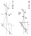
- Fig. 1A shows the main part of the optical system of a fingerprint input apparatus according to the present invention.
- reference symbol A-B denotes the fingerprint collection surface of a prism 1;
- C'-D' a pinhole plate surface having a pinhole PH formed in its center;
- O the center of the pinhole PH.
- the prism 1 is assumed to have the same refractive index as that of air.
- an LED is placed on the lower surface side of the prism 1 such that light from the LED is irradiated on the fingerprint collection surface A-B through the prism 1. Note that this LED may be a laser beam radiator.
- Light emitted from an LED or laser beam radiator has a single wavelength and is less in optical irregularity than light from an incandescent lamp. Owing to such characteristics, the LED allows a high resolution, and has a long service life. In addition, the heat generated by the LED exerts little influence on the apparatus.
- the light reflected by the fingerprint surface of the finger placed on the fingerprint collection surface A-B and emerging from the prism 1 passes through the pinhole PH and is formed into an image on an imaging plane I-J.
- no fingerprint image blur occurs. That is, both distortion and a blur can be prevented at once.
- the prism 1 is assumed to have the same refractive index as that of air. In practice, however, the refractive index of the prism 1 differs from that of air. For this reason, as shown in Fig. 1B, a surface equivalent to the fingerprint collection surface A-B when the prism 1 is substituted by air is set as an optical fingerprint collection surface A'-B' (a curved surface A'-B' indicated by the dotted line in Fig. 1B), and this optical fingerprint collection surface A'-B' and the imaging plane I-J are set to be parallel to each other.
- an optical fingerprint collection surface A'-B' a curved surface A'-B' indicated by the dotted line in Fig. 1B
- the position and size of the fingerprint image on the imaging plane I-J can be adjusted by adjusting the position of the pinhole PH in the back-and-forth direction (Z direction), the lateral direction (X direction), and the vertical direction (Y direction).
- Z direction back-and-forth direction
- X direction lateral direction
- Y direction vertical direction
- the fingerprint input section 10-3 includes a light source (LED) 10-31, a diffusion plate 10-32, a prism 10-33, a pinhole plate 10-34, a pinhole position adjusting mechanism 10-35, and a light-receiving unit 10-36.
- LED light source
- a total reflection method is used for the fingerprint input section 10-3 such that the LED 10-31 is placed on the left side of the lower surface side of the prism 10-33, and light from the LED 10-31 is irradiated on a fingerprint collection surface A-B of the prism 10-33 through the prism 10-33.
- a surface equivalent to the fingerprint collection surface A-B when the prism 10-33 is substituted by air is set as an optical fingerprint collection surface A'-B' (a curved surface A'-B' indicated by the dotted line in Fig. 3A), and this optical fingerprint collection surface A'-B' and an imaging plane I-J of the light-receiving unit 10-36 are set to be almost parallel to each other. That is, the straight line A'-B' and the imaging plane I-J are set to be parallel to each other.
- the LED 10-31 is placed on the right side of the lower surface side of the prism 10-33, and a black coating (or light-shielding plate) 10-37 is formed on the left-side surface of the prism 10-33 so that light from the LED 10-31 is irradiated on the fingerprint collection surface A-B through the prism 10-33.
- a surface equivalent to the fingerprint collection surface A-B when the prism 10-33 is substituted by air is set as an optical fingerprint collection surface A'-B' (a curved surface A'-B' indicated by the dotted line in Fig.
- this optical fingerprint collection surface A'-B' and the imaging plane I-J of the light-receiving unit 10-36 are set to be almost parallel to each other. That is, the straight line A'-B' and the imaging plane I-J are set to be parallel to each other.
- the formation of the black coating (or light-shielding plate) 37 on the left-side surface of the prism 10-33 can prevent externally incident disturbance light from influencing the apparatus.
- 3B and 4B respectively show the conventional arrangements of fingerprint input sections using the total reflection method and the optical path separation method.
- Each conventional arrangement uses an incandescent lamp 10-31' as a light source and a lens Ln for a light-receiving unit 10-36'.
- Figs. 5A and 5B show the fingerprint input apparatus 10.
- the fingerprint collection surface A-B of the prism 10-33 i.e., an upper surface UP of the prism 10-33
- a guide 10-41 is formed on a case 10-4 to allow an operator to put his/her finger on the upper surface UP of the prism 10-33 directly or indirectly (a film may be formed).
- the ten-key pad 10-1 and the display 10-2 are arranged side by side.
- the ten-key pad 10-1 has a fingerprint input confirmation key 10-11.
- Three-axis position adjusting knobs Cx, Cy, and Cz rotatably coupled to the pinhole position adjusting mechanism 10-35 are arranged on a side surface of the case 10-4.
- the fingerprint of a user is registered in the following manner.
- the user inputs an ID number assigned to him/her by using the ten-key pad 10-1 before using the system (step 101 in Fig. 7).
- the user then puts his/her finger on the upper surface UP (fingerprint collection surface A-B) of the prism 10-33 along the guide 10-41 of the fingerprint input apparatus 10.
- Light from the LED 10-31 has been irradiated on the fingerprint collection surface A-B of the prism 10-33, so the light from the LED 10-31 is totally reflected by the recess portions (groove portions) of the skin surface which are not in contact with the fingerprint collection surface A-B.
- the total reflection conditions are not satisfied, so the light from the LED 10-31 is scattered.
- the light reflected by the skin surface of the finger placed on the fingerprint collection surface A-B and emerging from the prism 10-33 passes through the pinhole PH and is formed into an image on the imaging plane I-J of the light-receiving unit 10-36.
- the fingerprint portion corresponding to the groove portions becomes bright, and the fingerprint portion corresponding to the ridge portions becomes dark. That is, a fingerprint image with a contrast is collected.
- the pattern of the collected fingerprint (registration fingerprint) is supplied as gray scale image data to the processing section 20.
- the user If the user sees his/her fingerprint image displayed on the display 10-2 and determines that the fingerprint image is out of position or excessively large or small, he/she determines that the position of the pinhole PH must be changed.
- the user then adjusts the angular positions of the three-axis position adjusting knobs Cx, Cy, and Cz to adjust the position of the pinhole plate 10-34 in the X, Y, and Z directions, i.e., the position of the pinhole PH in the X, Y, and Z directions, through the pinhole position adjusting mechanism 10-35, thereby setting the fingerprint image on the display 10-2 to a desired position in a desired size (steps 102 to 104).
- the control section 20-1 determines that loading of the registration fingerprint is confirmed (step 105), and the image data of the confirmed registration fingerprint is filed in the hard disk 20-4 in correspondence with the ID number (step 106).
- collation of the fingerprint of the user is performed as follows.
- the user inputs an ID number assigned to him/her by using the ten-key pad 10-1 (step 201 in Fig. 8), and then puts his/her finger on the upper surface UP (fingerprint collection surface A-B) of the prism 10-33 along the guide 10-41 of the fingerprint input apparatus 10.
- the pattern of the collected fingerprint (collation fingerprint) is supplied as halftone image data to the processing section 20 in the same manner as in the case of the registration of the fingerprint.
- control section 20-1 Upon reception of the ID number through the ten-key pad 10-1, the control section 20-1 reads out the image data of the registration fingerprint corresponding to the ID number from the registration fingerprints filed in the hard disk 20-4 (step 202), and displays it on the display 10-2 (step 203).
- the control section 20-1 also loads the image data of the collation fingerprint from the fingerprint input apparatus 10 through the frame memory 20-5 (step 204), and displays it on the display 10-2 while superimposing it on the fingerprint image of the registration fingerprint (step 205).
- Fig. 6B shows a display sample in this case. The user sees this superimposed state of the fingerprint image of the registration fingerprint and the fingerprint image of the collation fingerprint displayed on the display 10-2 to determine whether to change the position of the pinhole PH.
- the user sees the fingerprint image of the collation fingerprint displayed on the display 10-2 and determines that this fingerprint image is out of position or excessively large or small with respect to the fingerprint image of the registration fingerprint, he/she determines that the position of the pinhole PH must be changed.
- the user then adjusts the angular positions of the three-axis position adjusting knobs Cx, Cy, and Cz to adjust the position of the pinhole plate 10-34 in the X, Y, and Z directions, i.e., the position of the pinhole PH in the X, Y, and Z directions, through the pinhole position adjusting mechanism 10-35, thereby setting the fingerprint image of the collation fingerprint on the display 10-2 to a desired position in a desired size (steps 204 to 206).
- the control section 20-1 determines that loading of the collation fingerprint is confirmed (step 207).
- the fingerprint image of the confirmed collation fingerprint is collated with the fingerprint image of the previously readout registration fingerprint (step 208).
- the collation result is then displayed on the display 10-2 (step 209).
- a blur and distortion can be greatly reduced according to the above basic principle.
- the position and size of an input fingerprint image in a registration process can be set to a desired position and a desired size by manually adjusting the position of the pinhole PH with the three-axis position adjusting knobs Cx, Cy, and Cz.
- the positional offset between the input fingerprint images in registration and collation processes can be absorbed, and the difference between the sizes of the input fingerprint images can also be coped with.
- the position of the pinhole PH is manually adjusted with the three-axis position adjusting knobs Cx, Cy, and Cz in registration and collation processes.
- This position may be automatically adjusted.
- Figs. 9 and 10 show operations to be performed in registration and collation processes when the position of the pinhole PH is automatically adjusted.
- the user inputs an ID number assigned to him/her by using the ten-key pad 10-1 (step 301 in Fig. 9).
- the user then puts his/her finger on the upper surface UP (fingerprint collection surface A-B) of the prism 10-33 along the guide 10-41 of the fingerprint input apparatus 10.
- Light reflected by the pattern surface of the finger placed on the fingerprint collection surface A-B and emerging from the prism 10-33 passes through the pinhole PH and is formed into an image on the imaging plane I-J of the light-receiving unit 10-36.
- the fingerprint portion corresponding to the groove portions becomes bright, and the fingerprint portion corresponding to the ridge portions becomes dark. That is, a fingerprint image with a contrast is collected.
- the pattern of the collected fingerprint (registration fingerprint) is supplied as halftone image data to the processing section 20.
- the loaded image data (Fig. 11A) of the registration fingerprint is divided into n x m pixels (Fig. 11B). That is, the loaded image data of the registration fingerprint is divided into n pixels in the x direction and m pixels in the y direction.
- I ij be the light intensity at the position of the ijth pixel
- x- and y-coordinates xa and ya of the barycenter are obtained according to equations (1) and (2):
- xa ( i n j m iI ij )/( i n j m I ij )
- the control section 20-1 obtains the difference (xa - xs, ya - ys) between the obtained barycentric position (xa, ya) and the set barycentric position (xs, ys) as a barycentric difference, and checks whether there is a barycentric difference (step 304). If there is a barycentric difference (barycentric difference ⁇ 0), the control section 20-1 adjusts the position of the pinhole PH in the X and Y directions through the pinhole position adjusting mechanism 10-35 so as to eliminate the barycentric difference (step 305).
- control section 20-1 causes the flow to advance to step 306 to load the image data of the registration fingerprint as the image data of the registration fingerprint whose positions in the X and Y directions are confirmed (step 306).
- the control section 20-1 calculates the size of the loaded image data of the registration fingerprint (step 307). In this case, the size is calculated in the following manner.
- the image data (Fig. 12A) of the registration fingerprint whose positions in the X and Y directions are confirmed is divided into n x m pixels (Fig. 12B). That is, the loaded image data of the registration fingerprint is divided into n pixels in the x direction and m pixels in the y direction. Each pixel is then binarized according to its light level such that each portion with light is represented by "1", and each of the remaining portions is represented by "0".
- the control section 20-1 compares this area Sa with a set area Ss to check whether the area Sa is appropriate (step 308). If the area Sa is not appropriate (Sa ⁇ Ss), the control section 20-1 adjusts the position of the pinhole PH in the Z direction through the pinhole position adjusting mechanism 10-35 to set the area Sa to an appropriate value (step 309). If Sa - Ss > 0, the control section 20-1 moves the position of the pinhole PH to reduce the fingerprint image. If Sa - Ss ⁇ 0, the control section 20-1 moves the position of the pinhole PH to enlarge the fingerprint image.
- control section 20-1 causes the flow to advance to step 310 to file the corresponding image data of the registration fingerprint as the image data of the registration fingerprint whose positions in the X, Y, and Z directions are confirmed in the hard disk 20-4 in correspondence with the ID number (step 310).
- the user inputs an ID number assigned to him/her by using the ten-key pad 10-1 (step 401 in Fig. 10), and puts his/her finger on the upper surface UP (fingerprint collection surface A-B) of the prism 10-33 along the guide 10-41 of the fingerprint input apparatus 10.
- the pattern of the collected fingerprint (collation fingerprint) is supplied as halftone image data to the processing section 20.
- the control section 20-1 Upon reception of the ID number through the ten-key pad 10-1, the control section 20-1 reads out the image data of the registration fingerprint corresponding to the ID number from the registration fingerprints filed in the hard disk 20-4 (step 402). The control section 20-1 loads the image data of the collation fingerprint from the fingerprint input apparatus 10 through the frame memory 20-5 (step 403). The control section 20-1 then calculates the barycentric position of the loaded image data of the collation fingerprint in the same manner as in the case of the registration fingerprint (step 404).
- the control section 20-1 obtains the difference (xb - xs, yb - ys) between the calculated barycentric position (xb, yb) and the set barycentric position (xs, ys) to check whether there is a barycentric difference (step 405). If there is a barycentric difference (barycentric difference ⁇ 0), the control section 20-1 adjusts the position of the pinhole PH in the X and Y directions through the pinhole position adjusting mechanism 10-35 (step 406).
- control section 20-1 causes the flow to advances to step 407 to load the image data of the collation fingerprint as the image data of a collation fingerprint whose positions in the X and Y directions are confirmed (step 407).
- the control section 20-1 then calculates the size of the loaded image data of the collation fingerprint in the same manner as in the case of the registration fingerprint (step 408).
- the control section 20-1 compares the calculated area Sb of the image data of the collation fingerprint, whose positions in the X and Y directions are confirmed, with the set area Ss to check whether the area Sb is appropriate (step 409). If the area Sb is not appropriate (Sb ⁇ Ss), the control section 20-1 adjusts the position of the pinhole PH in the Z direction through the pinhole position adjusting mechanism 10-35 to set the area Sb to an appropriate value (step 410). That is, if Sb - Sb > 0, the control section 20-1 moves the position of the pinhole PH to reduce the fingerprint image. If Sb - Ss ⁇ 0, the control section 20-1 moves the position of the pinhole PH to enlarge the fingerprint image.
- position adjustment in the Z direction is performed after position adjustment in the X and Y directions according to the flow chart shown in Figs. 9 and 10, position adjustment in the X and Y directions may be performed after position adjustment in the Z direction.
- the imaging plane I-J is rotated about a point PO through a predetermined angle to set an imaging plane U-T (see Fig. 13A) so as to eliminate the distortion of the optical fingerprint collection surface A'-B'.
- the distortion caused on the fingerprint collection surface A-B can be greatly reduced.
- a triangular prism is used as the prism 1 (10-33).
- a rectangular prism 1' (10-33') like the one shown in Fig. 15 may be used.
- Various other types of prisms may be used.
- the diffusion plate 10-32 may be mounted on the prism 1' (10-33') side, as indicated by the dotted line.
- the prism is defined as an optical element having two or more flat surfaces and using refraction and reflection of light.
- the functions of the prism are defined as functions 1 ⁇ to 3 ⁇ as follows.
- the total reflection method is used for the fingerprint input section 10-3. Even if the optical separation method is used, however, the same operations described above can be applied to the resultant arrangement. It cannot be said that one of the total reflection method and the optical path separation method is superior to the other.
- Embodiment 1 (see Fig. 1A), the diameter of the pinhole PH must be decreased to some degree to increase the resolution of a fingerprint image. For this reason, the light intensity of a fingerprint image formed on the imaging plane I-J decreases. To compensate for this, the intensity of light from a light source which is irradiated on the fingerprint collection surface A-B must be increased. As a result, the service life of the light source itself is shortened because of the heat generated by the light source, or the light transmitted through the prism 1 is too bright for the user, thus posing new problems. To solve such problems, a near infrared light-emitting diode may be used as a light source. In this case, although glaring can be suppressed, the problem of the generation of heat cannot be solved.
- a lens 5-2 is placed near the rear surface of a pinhole plate 5-1, as shown in Fig. 17, to increase the light intensity of a fingerprint image formed on an imaging plane 5-3 without increasing the intensity of light from a light source 6.
- a straight line connecting the center of a fingerprint collection surface 1-1 and the center of the imaging plane 5-3 is an optical axis
- the central axis of the lens 5-2 is made to coincide with the optical axis.
- reference numeral 1-2 denotes a black coating (or light-shielding plate) formed on the left-side surface of a prism 1.
- the image magnification is determined by the ratio of a line segment Ox to a line segment OX.
- a triangle OAB is not similar to a triangle Oab, and a line segment OA is shorter than a line segment OB, the image on the point A side becomes large, whereas the image on the point B side becomes small.
- This trapezoidal distortion increases as the ratio of OA : OB increases.
- the distance between the fingerprint collection surface and the lens must be decreased. If this distance is decreased, the ratio of OA : OB increases, resulting in greater trapezoidal distortion.
- the light intensity of a fingerprint image formed on the imaging plane 5-3 can be increased without increasing the light intensity of the light source 6, and the occurrence of trapezoidal distortion is greatly suppressed under the condition in which a blur is suppressed, thereby obtaining a high-quality fingerprint image.
- Fig. 20A shows the main part of a fingerprint input apparatus according to the present invention (Embodiment 2-1).
- a lens having barrel distortion negative distortion
- a central axis LC of the lens 5-2 is inclined, by ⁇ 1, to the B point side on the fingerprint collection surface A-B side with respect to an optical axis LO (a straight line connecting a center X o of a fingerprint collection surface A-B and a center x o of an imaging plane a-b).
- an optical axis LO a straight line connecting a center X o of a fingerprint collection surface A-B and a center x o of an imaging plane a-b.
- the inclination of the imaging plane a-b with respect to the optical axis LO is adjusted.
- Fig. 20B shows the main part of a fingerprint input apparatus according to the present invention (Embodiment 2-2).
- a lens having pincushion distortion positive distortion
- a central axis LC of the lens 5-2 is inclined, by ⁇ 2, to the point A side on a fingerprint collection surface A-B with respect to an optical axis LO.
- the inclination of an imaging plane a-b is adjusted with respect to the optical axis LO.
- the pinhole serves to increase the degree of freedom in design. That is, since the pinhole is formed in front of the lens, the depth of focus of the lens increases, and a tolerance can be ensured for the angle defined by the imaging plane and the optical axis that causes no blur, thereby satisfactorily increasing the degree of freedom in design.
- the optical system of the fingerprint input apparatus is designed as follows:
- a fingerprint input apparatus includes an optical system as a constituent, and a reduction in the size of the apparatus is required in consideration of the installation place, operability, and the like.
- the size of this fingerprint input apparatus can be effectively reduced by forming an optical system according to the optical path separation method and placing a light source and a prism close to each other.
- Fig. 23 shows the main part of a conventional fingerprint input apparatus using the optical path separation method.
- reference numeral 1 denotes a prism; 3, a light-receiving unit; and 6, a light source.
- the light source 6 is placed on the right side of the lower surface side of the prism 1.
- a black coating (or light-shielding plate) 1-2 is formed on the left-side surface of the prism 1 to irradiate light from the light source 6 on a fingerprint collection surface 1-1 through the prism 1.
- light from the light source 6 is reflected by the pattern surface of a finger placed on the fingerprint collection surface 1-1 and emerges from the prism 1 to be formed into an image on an imaging plane (CCD) 3-2 through a lens 3-1.
- CCD imaging plane
- Fig. 24 shows the main part of a fingerprint input apparatus using the total reflection method.
- a light source 6 is placed on the left side of the lower surface side of a prism 1, and light from the light source 6 is irradiated on a fingerprint collection surface 1-1 through a diffusion plate 7 and the prism 1.
- a reduction in the size of the apparatus is limited.
- the fingerprint input apparatus using the optical path separation method has an advantage in terms of a reduction in size. If, however, the light source 6 and the prism 1 are brought close to each other to further reduce the size, the incident angle on the illumination light incident surface of the prism 1 increases, and light is refracted and diffused. As a result, the fingerprint collection surface 1-1 of the prism 1 partly decreases in illuminance, leading to illuminance irregularity.
- Embodiment 3 therefore, the light source 6 and the prism 1 are placed close to each other to attain a reduction in size without causing any illuminance irregularity on the fingerprint collection surface 1-1. That is, both a reduction in the size of the apparatus and an improvement in the quality of a fingerprint image are attained at once.
- the cut surface 1-3 is formed under conditions 1 ⁇ , 2 ⁇ , and 3 ⁇ below:
- n1 and n2 be the refractive indexes of the media
- the condition in which an image of the light source 6 is not projected on the imaging plane 3-2 is that the light source 6 is located in the hatched region under a straight line extending from a point B to a point O.
- ⁇ be the angle defined by points A, B, and E of the prism 1
- ⁇ be the incident angle of light from a point O to a point B with respect to a surface A-B
- ⁇ be the angle at which light reflected at the point B is refracted on a surface B-E of the prism and emerges to an end point b of the imaging plane 3-2
- a reflected image of the light source 6 is not projected on the imaging plane 3-2 as long as the light source 6 is located at a position within the range of ⁇ ⁇ ⁇ - sin -1 (sin ⁇ /n2) (the hatched region in Fig. 28).
- condition for the cut surface 1-3 is that light from the light source 6 is not totally reflected by the fingerprint collection surface 1-1 regardless of the position of the light source 6.
- condition 3 ⁇ is not an absolutely necessary condition, and the cut surface 1-3 may be formed under conditions 1 ⁇ and 2 ⁇ alone.
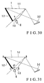
- Embodiment 3-1 when at least conditions 1 ⁇ and 2 ⁇ are to be satisfied, the cut surface 1-3 decreases in size, and the light source 6 may not be positioned.
- an inclined surface may be formed as a cut surface 1-3 to increase its size, as shown in Fig. 30.
- the cut surface 1-3 is excessively inclined with respect to a fingerprint collection surface 1-1.
- the fingerprint collection surface 1-1 cannot be uniformly illuminated. That is, the left end of the fingerprint collection surface 1-1 is mainly illuminated by a light source 6, and hence the fingerprint collection surface 1-1 cannot be uniformly illuminated.
- condition 1 ⁇ is satisfied, but 2 ⁇ is not satisfied (reflection condition based on Fresnel's formulas). That is, a region C-F on the cut surface 1-3 becomes a region which does not satisfy condition 2 ⁇ .
- a black coating (or light-shielding plate) 1-2 is formed on the area C-F which does not satisfy condition 2 ⁇ .
- any light shield may not be required for the region which does not satisfy condition 2 ⁇ .
- a wall 8 is provided to prevent disturbance light from entering the optical system, stray light propagating from the light source 6 to the wall 8 may be incident on an imaging plane 3-2 through the optical path "G ⁇ H ⁇ I ⁇ J".
- the region C-F is shielded against stray light emitted from the light source 6 and reflected by the wall 8, and no stray light is incident on the imaging plane 3-2.
- the cut surface 1-3 of the prism 1 is flat. In this case, light from the light source 6 is refracted by the cut surface 1-3, and the directivity increases. Strictly speaking, therefore, the peripheral portion of the fingerprint collection surface 1-1 becomes darker than the central portion.
- Embodiment 3-4 therefore, the outer periphery of a concave cut surface 1-3 is formed into a convex surface, as shown in Fig. 33B.
- light from a light source 6 is diffused by a concave surface 1-3a of the central portion of the cut surface 1-3, focused by a convex surface 1-3b of the outer periphery of the cut surface 1-3, and irradiated on a fingerprint collection surface 1-1, thereby compensating the light intensity distribution on an imaging plane 3-2.
- the cut surface 1-3 is formed on the prism 1 to improve illumination irregularity on the fingerprint collection surface 1-1.
- a light source 6 is placed close to a prism surface B-E through a matching member 9 having a high refractive index.
- No cut surface 103 is formed on a prism 1.
- a refractive index matching solution As a material for the matching member 9, a refractive index matching solution is known. However, a material other than this solution, e.g., an epoxy-based adhesive, may be used as long as the difference between the refractive indexes of the prism 1 and the material does not greatly influence the uniformity of illumination on the fingerprint collection surface 1-1.
- an epoxy-based adhesive e.g., an epoxy-based adhesive
- a cut surface 1-3 may be formed on the prism 1, and the light source 6 may be placed close to the cut surface 1-3 through the matching member 9.
- Embodiment 3-5 a high-quality fingerprint image can be obtained with a compact apparatus, and the following additional effect can also be obtained. Since heat generated by the light source 6 is radiated onto the prism 1 through the matching member 9, perspiration of the finger is stimulated. As a result, a clear fingerprint image can be obtained.
- Fig. 35 shows the main part of a conventional fingerprint input apparatus.
- reference numeral 6 denotes a light source (LED); 11, a substrate having a front surface 11F on which the LED 6 is mounted; 1, a prism; and 3, a light-receiving unit.
- This apparatus uses the optical path separation method.
- the substrate 11 having the LED 6 mounted thereon is placed on the right side of the lower surface side of the prism 1, and a black coating (or light-shielding plate) 1-2 is formed on the left-side surface of the prism 1.
- a black coating or light-shielding plate
- light from the LED 6 is irradiated on the a fingerprint collection surface A-B through the prism 1.
- light reflected by the pattern surface of a finger placed on the fingerprint collection surface A-B and emerging from the prism 1 is formed into an image on an imaging plane (CCD) 3-2 through a lens 3-1 of the light-receiving unit 3.
- CCD imaging plane
- a reflecting mirror 12 like the one indicated by the dotted lines in Fig. 35 may be placed on the rear surface side of the substrate 11 to cause light transmitted through the side surfaces of the LED 6 and the substrate 11 and leaking out from the rear surface 11R to be incident on the prism 1.
- the number of parts increases, leading to an increase in cost and interfering with a reduction in size.
- the light intensity decreases.
- Embodiment 4 therefore, a high-quality fingerprint image is obtained at a low cost without interfering with a reduction in size.
- Fig. 36 shows the main part of a fingerprint input apparatus according to the present invention.
- the same reference numerals in Fig. 36 denote the same parts as in Fig. 35, and a description thereof will be omitted.
- a film (reflecting film) 11-1 having a high reflectance is formed on a front surface 11F of a substrate 11, i.e., the front surface 11F of the substrate 11 on which an LED 6 is mounted.
- Figs. 37A and 37B show how the reflecting film 11-1 is formed on the substrate 11.
- Power supply electrode pads PA and PB and LED electrode pads P1 1 , P1 2 , P2 1 , P2 2 , P3 1 , P3 2 , P4 1 , P4 2 , P5 1 , P5 2 , P6 1 , and P6 2 are formed on the front surface 11F of the substrate 11 by etching a metal film.
- the reflecting film 11-1 is formed on the entire region of the substrate except for the portions where these electrode pads are formed.
- a coating method, a printing method, or the like may be used to form the reflecting surface 11-1.
- the reflecting film 11-1 is formed on the front surface 11F of the substrate 11 by a screen printing method using a white coating material. Since the reflectance of the white coating material for screen printing is 80%, light can be efficiently reflected. In addition, since the white coating material diffuses/reflects light, a uniform light intensity distribution with little directivity can be realized. Furthermore, element numbers and the like are printed on the substrate 11 by screen printing, and the reflecting film 11-1 can be formed in the same process as this printing process, this method is advantageous in terms of cost.
- an LED 6-1 is connected to the LED pads P1 1 and P1 2 through solder portions F
- an LED 6-2 is connected to the LEDs P2 1 and P2 2 through solder portions F
- an LED 6-3 is connected to the LED pads P3 1 and P3 2 through solder portions F
- an LED 6-4 is connected to the LED pads P4 1 and P4 2 through solder portions F
- an LED 6-5 is connected to the LED pads P5 1 and P5 2 through solder portions F
- an LED 6-6 is connected to the LED pads P6 1 and P6 2 through solder portions F.
- a film (light-shielding film) 11-1' for shielding light is formed on a front surface 11F of a substrate 11 on which an LED 6 is mounted.
- the light-shielding film 11-1' is formed by screen printing. Note, however, that a black coating material for screen printing is used for the light-shielding film 11-1'. Since the light-shielding film 11-1' is black, light is absorbed into the coating material, thus preventing the light from passing through a rear surface 11R of the substrate 11.
- the light-shielding film 11-1' is formed on the entire region of the substrate except for the portions where electrode pads P are formed. If, however, the print portion overlaps the pad portions to such an extent that no influence is exerted on bonding of the LEDs 6-1 to 6-6, leakage of light can be prevented more effectively. That is, the light-shielding characteristics improve.
- a film (reflecting/light-shielding film) 11-1'' having a high reflectance and serving to shield light is formed on a front surface 11F of a substrate 11 on which an LED 6 is mounted.
- the reflecting/light-shielding film 11-1'' is formed by screen printing.
- a white coating material for screen printing is used for the reflecting/light-shielding film 11-1'', and the film is formed thick. Since the white coating material is printed thick, light is diffused/reflected by the front surface 11F of the substrate 11. Although the absorbance of the white coating material is low, a larger amount of light can be absorbed with an increase in the thickness of the film. Even a white coating material can shield light depending on the film thickness.
- Embodiment 4-3 as in Embodiment 4-2, if the print portion overlaps the pad portions to such an extent that no influence is exerted on bonding of the LEDs 6-1 to 6-6, leakage of light can be prevented more effectively, and the light-shielding characteristics improve.
- the reflecting/light-shielding film 11-1'' is formed by screen printing.
- a reflecting/light-shielding film 11-1'' is formed by using a metal film.
- Electrodes PA, PB, P1 1 , P1 2 to P6 1 , and P6 2 are to be formed on a front surface 11F of a substrate 11 by etching, gaps are ensured around the respective electrode pads P, and a metal film is left outside the gaps (see Fig. 39A). This left metal film is the reflecting/light-shielding film 11-1''.
- Embodiment 4-4 using the metal film as the reflecting/light-shielding film 11-1'', the same effects as those of Embodiment 4-3 can be obtained.
- relatively thick white coatings are formed on gaps G (GA, GB, G1 1 , G1 2 to G6 1 , and G6 2 ) ensured around the respective pads P by screen printing. With these coatings, the respective pads P can be reliably insulated from each other, and the light-shielding characteristics can be improved.
- a reflecting film 11-1, a light-shielding film 11-1', or a reflecting/light-shielding film 11-1'' is formed on a front surface 11F of the substrate 11 having the LED 6 mounted thereon in the same manner as in the case of the fingerprint input apparatuses using the optical separation method.
- the collation precision of a fingerprint collation system greatly depends on whether a fingerprint image can be properly input.
- disturbances affecting a fingerprint image input operation include dust and the like adhering to an optical system including a prism and a lens and disturbance light entering the imaging plane of a CCD. If disturbance light enters the imaging plane, a fingerprint image is made dim. A clear, high-contrast fingerprint image cannot therefore be obtained.
- a main body case for covering the overall fingerprint input apparatus is made to have a hermetic structure to protect the apparatus against such disturbances.
- Fig. 41 shows the main part of a conventional fingerprint input apparatus.
- reference numeral 6 denotes a light source; 1, a prism; 13, a prism holder; 3, a light-receiving unit; and 14, a main body case.
- the light source 6 is placed on the right side of the lower surface side of the prism 1.
- the prism 1 is held by the prism holder 13.
- the prism holder 13 is fixed to the main body case 14 such that a fingerprint collection surface 1-1 of the prism 1 opposes a finger mount portion opening 14-1 of the main body case 14.
- the light-receiving unit 3 includes a lens 3-1, an imaging plane (CCD) 3-2, and an imaging plane case 3-3.
- the main body case 14 has a hermetic structure.
- the main body case 14 having a hermetic structure prevents dust and the like from adhering to the optical system including the lens 3-1 and the like, and also prevents external light (disturbance light 1 ⁇ ) from entering the imaging plane 3-2.
- Embodiment 5 is therefore designed to reliably prevent dust and the like from adhering to an optical system and prevent disturbance light from entering the imaging plane 3-2 without making the main body case 14 have a hermetic structure, thereby obtaining a high-quality fingerprint image.
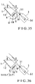
- a light-shielding cover 15 is placed between a prism 1 and a light-receiving unit 3' to cover an imaging optical path between an exit surface 1-4 of the prism 1 and an imaging plane 3-2 while isolating the optical path from the outside.
- a prism holder 13' for holding the prism 1 has openings 13-1 and 13-2 formed in surface portions opposing the exit surface 1-4 of the prism 1 and an incident surface 1-5 on which light from a light source 6 is incident (see Fig. 43).
- An opening 15-1 of the light-shielding cover 15 on one end side is coupled to the opening 13-1 of the prism holder 13' with a fitting structure
- An opening 15-2 of the light-shielding cover 15 on the other side is also coupled to an opening 3-3a of an imaging plane cover 3-3' with a fitting structure. Note that many air holes 14-2 are formed in a body case 14'.
- the light-shielding cover 15 prevents dust and the like from adhering to the optical system including the lens 3-1 and the like; external light (disturbance light 1 ⁇ ) from entering the imaging plane 3-2 through the air holes 14-2; and light (disturbance light 2 ⁇ ) emitted from the light source 6 from detouring the prism 1 and entering the imaging plane 3-2.
- the black matte coating is formed on the surface of the inner wall of the light-shielding cover 15 to prevent disturbance light 3 ⁇ from entering the imaging plane 3-2.
- an optical noise process may be performed by a method of forming a velvety coating surface by electrostatic coating, a method of forming the surface of the inner wall into an uneven surface, and the like as well as the method of forming a black matte coating. That is, entrance of light 3 ⁇ into the imaging plane 3-2 is prevented by absorbing or diffusely reflecting the light incident on the surface of the inner wall of the light-shielding cover 15.
- a film having a high reflectance is formed on the surface of the outer wall of the light-shielding cover 15.
- the light-shielding cover 15 is coupled to the main body by a fitting structure, an optical system positioning effect can be obtained.
- the frame and the cover are tightly coupled to each other without any gap, the light-shielding effect and the dustproof effect improve.
- the light-shielding cover 15 is temporarily secured to the main body with a fitting structure, and is fastened to the main body with screws or the like afterward, the reinforcing effect improves.
- Fig. 44 shows the main part of a fingerprint input apparatus according to the present invention (Embodiment 5-2).
- a light source cover 16 is provided for a light source 6'.
- the light source cover 16 covers the light source 6' except for a portion on the exit surface side with respect to a prism 1.
- the light source cover 16 and a light-shielding cover 15 are integrally formed.
- the illumination efficiency of the light source 6' with respect to the prism 1 is improved by the light source cover 16.
- the number of parts and the number of manufacturing steps can be decreased, thus attaining a reduction in cost.
- the light source cover 16 is positioned at the same time, thus facilitating an assembly operation and shortening the time required for assembly.
- the molds are drawn in the same direction. For this reason, no extra mold is required.
- an optical noise process is performed for the surface of the inner wall of the light-shielding cover 15, a film having a high reflectance is formed on the surface of the outer wall of the light-shielding cover 15 or the light source cover 16, and the integrally formed light-shielding cover 15 and light source cover 16 are coupled to the main body with a fitting structure.
- a film having a high reflectance is formed on the surface of the inner wall of the light source cover 16 the reflectance increases, and the illumination efficiency improves.
- the lens 3-1 is used to form a fingerprint image on the imaging plane 3-2.
- a pinhole may be used in place of the lens 3-1.
- Embodiment 5-1 the optical system is arranged according to the optical path separation method, but may be arranged according to the total reflection method.
- the total reflection method the light source 6 is placed on the left side of the lower surface side of the prism 1, and light from the light source 6 is irradiated on the fingerprint collection surface 1-1 through the prism 1.
- Embodiment 5-2 (Fig. 44) is suited for a case in which the optical system is arranged according to the optical path separation method.
- the optical system on the first prism side and the optical system on the second prism side are set to be similar to each other.
- light reflected by the pattern surface of a finger placed directly or indirectly on the fingerprint collection surface and emerging from the first prism passes through the pinhole to be formed into an image on the imaging plane through the second prism.
- a blur and distortion can be eliminated at once, and hence a high-quality fingerprint image can be obtained.
- the imaging plane is inclined with respect to the optical axis to prevent a blur
- the central axis of the lens is inclined with respect to the optical axis to prevent trapezoidal distortion.
- the ninth aspect light from the light source is incident on the prism through the cut surface and irradiated on the fingerprint collection surface with an almost uniform diffusion angle.
- the light can therefore be placed near the prism to realize a compact structure without causing illumination irregularity on the fingerprint collection surface. That is, both a reduction in the size of the apparatus and an improvement in the quality of a fingerprint image can be realized at once.
- the imaging optical path of light propagating from the fingerprint collection surface to the imaging plane is not shielded within the prism, and an image of the light source is not projected on the imaging plane. For this reason, both a reduction in the size of the apparatus and an improvement in the quality of a fingerprint image can be realized at once.
- the imaging optical path of light propagating from the fingerprint collection surface to the imaging plane is not shielded within the prism, and an image of the light source is not projected on the imaging plane.
- light from the light source is not totally reflected by the fingerprint collection surface.
- the effect of preventing total reflection from adversely affecting a fingerprint image can be obtained.
- the imaging optical path of light propagating from the fingerprint collection surface to the imaging plane is not shielded within the prism, and there is no possibility that an image of the light source is projected on the imaging plane owing to the light-shielding effect provided for the cut surface.
- the size of the apparatus can therefore be further reduced by increasing the cut surface.
- the 13th aspect light from the light source is incident on the prism through the concave cut surface.
- illumination to the fingerprint collection surface can be made uniform as compared with a case in which a flat cut surface is formed.
- light from the light source is diffused by the concave inner surface of the cut surface and is focused by the convex surface of the outer periphery of the cut surface to be irradiated on the fingerprint collection surface.
- the light intensity distribution on the imaging plane can be made uniform.
- the prism need not have a cut surface.
- heat generated by the light source is radiated to the prism through the matching member, perspiration of the finger is stimulated. As a result, an additional effect of obtaining a clear fingerprint image can be obtained.
- the 16th aspect light leaking from the side and rear surfaces of the light source is reflected by the reflecting film on the substrate surface and incident on the prism.
- the illumination efficiency for the fingerprint collection surface improves, and hence a high-quality fingerprint image can be obtained at a low cost without interfering with a reduction in size.
- the 18th aspect light leaking from the side and rear surfaces of the light source is reflected by the reflecting/light-shielding film on the substrate surface to be incident on the prism.
- the light leaking from the side and rear surfaces of the light source is shielded by the reflecting/light-shielding film on the substrate surface to be prevented from passing through the substrate and leaking out from the rear surface.
- the light-shielding cover for covering the imaging optical path between the exit surface and imaging plane of the prism while isolating the optical path from the outside is used to reliably prevent dust and the like from adhering to the optical system; and disturbance light (disturbance light 1 ⁇ and 2 ⁇ ) from entering the imaging plane, thereby obtaining a high-quality fingerprint image.
- the light-shielding cover serves as a reinforming member, the positional relationship between the components of the optical system can be reliably maintained against vibrations and external forces. Offsets (size, position, and distortion) of a formed image can therefore be prevented, and a fingerprint image can be stably input.
- disturbance light (disturbance light 3 ⁇ ) emerging from the prism can be prevented from entering, as optical noise, the imaging plane.
- the high-reflectance film is formed on the surface of the outer wall of the light-shielding cover in the 19th or 20th aspect, light which is not directly irradiated from the light source onto the prism is reflected by the high-reflectance film to be incident on the prism. As a result, the illumination efficiency improves.
- the light source cover covers the light source except for the exit surface side with respect to the prism, the illumination efficiency for the prism improves.
- the light-shielding cover and the light source cover are integrally formed, the number of parts decreases. As a result, a reduction in cost can be attained.
- the opening of the light-shielding cover on one end side is coupled to the opening of the prism holder which opposes the exit surface of the prism with the fitting structure, and the opening of the light-shielding cover on the other side is coupled to the opening of the imaging plane case with the fitting structure.
- the three members i.e., the prism (prism holder), the light-shielding cover, and the imaging plane cover, can be easily secured temporarily.
- the coupling portions have no gaps, the light-shielding effect and the dustproof effect can be improved as well as the optical system positioning effect.
Abstract
Description
Claims (24)
- A fingerprint input apparatus characterized by comprising:a prism (1) placed such that a surface in one direction serves as a fingerprint collection surface (A-B);a light source (10-31) for irradiating light on the fingerprint collection surface through said prism;a pinhole (PH) set in a path of light which is reflected by a pattern surface of a finger placed on said fingerprint collection surface and emerges from said prism; andan imaging plane (I-J) on which the light emerging from said prism and passing through said pinhole is formed into an image,
wherein when said prism is substituted by air, an optical fingerprint collection surface equivalent to the fingerprint collection surface is set to be substantially parallel to said imaging plane. - An apparatus according to claim 1, wherein when the optical fingerprint collection surface has distortion with respect to the fingerprint collection surface, said imaging plane is rotated through a predetermined angle.
- A fingerprint input apparatus characterized by comprising:a first prism (1) placed such that a surface in one direction serves as a fingerprint collection surface (A-B);a light source (10-31) for irradiating light on the fingerprint collection surface through said first prism;a pinhole (PH) set in a path of light which is reflected by a pattern surface of a finger placed on said fingerprint collection surface and emerges from said first prism;an imaging plane (I-J) on which the light emerging from said first prism and passing through said pinhole is formed into an image; anda second prism (4) placed in front of said imaging plane,
wherein the fingerprint collection surface of said first prism is set to be substantially parallel to said imaging plane, the fingerprint collection surface of said first prism is set to be substantially parallel to a surface of said second prism on the imaging plane side, and an exit surface of said first prism with respect to said pinhole is set to be substantially parallel to an incident surface of said second prism with respect to said pinhole. - An apparatus according to any one of claims 1, 2, and 3, further comprising pinhole position adjusting means (10-35) for adjusting a position of said pinhole.
- An apparatus according to claim 4, wherein said pinhole position adjusting means is constituted by a manual adjusting mechanism, and said apparatus further comprises a display section (10-2) for displaying a fingerprint image formed on said imaging plane.
- An apparatus according to claim 4, wherein said pinhole position adjusting means automatically adjusts the position of said pinhole.
- An apparatus according to any one of claims 1, 2, and 3, wherein said light source is an LED or a laser beam radiator.
- A fingerprint input apparatus characterized by comprising:a prism (1) placed such that a surface in one direction serves as a fingerprint collection surface (A-B);a light source (6) for irradiating light on the fingerprint collection surface through said prism;a pinhole set in a path of light which is reflected by a pattern surface of a finger placed on said fingerprint collection surface and emerges from said prism;a lens (5-2) placed close to a rear side of said pinhole; andan imaging plane (a-b) on which the light emerging from said prism and passing through said pinhole and said lens is formed into an image,
wherein when a straight line connecting a center of the fingerprint collection surface and a center of said imaging plane is an optical axis, said imaging plane is inclined with respect to the optical axis to prevent a blur, and a central axis of said lens is inclined with respect to the optical axis to prevent trapezoidal distortion. - A fingerprint input apparatus, in whicha prism (1) placed such that a surface in one direction serves as a fingerprint collection surface (1-1),a light source (6) for irradiating light on the fingerprint collection surface through said prism, andan imaging plane (3-2) on which light reflected by the fingerprint collection surface and emerging from said prism is formed into an imageare arranged by an optical path separation method,
characterized in that a cut surface (1-3) is formed at a distance from a vertex of said prism which opposes the fingerprint collection surface, andsaid light source is placed to oppose the cut surface of said prism. - An apparatus according to claim 9, wherein the cut surface is formed under conditions that an imaging optical path of light from the fingerprint collection surface to said imaging plane is not prevented, and an image of said light source is not projected on said imaging plane.
- An apparatus according to claim 9, wherein the cut surface is formed under conditions that an imaging optical path of light from the fingerprint collection surface to said imaging plane is not prevented, an image of said light source is not projected on said imaging plane, and light from said light source is not totally reflected by the fingerprint collection surface.
- An apparatus according to claim 9, wherein the cut surface is formed under a condition that an imaging optical path of light from the fingerprint collection surface to said imaging plane is not prevented, and a light shield is provided for a region, on the cut surface, on which an image of said light source can be projected.
- An apparatus according to any one of claims 9 to 12, wherein the cut surface of said prism is a concave surface.
- An apparatus according to claim 13, wherein the cut surface of said prism has a convex outer periphery.
- A fingerprint input apparatus, in whicha prism (1) placed such that a surface in one direction serves as a fingerprint collection surface (1-1),a light source (6) for irradiating light on the fingerprint collection surface through said prism, andan imaging plane (3-2) on which light reflected by the fingerprint collection surface and emerging from said prism is formed into an imageare arranged by an optical path separation method,
characterized in that said light source is placed in contact with said prism through a matching member (9) having a predetermined refractive index. - A fingerprint input apparatus comprising:a prism (1) placed such that a surface in one direction serves as a fingerprint collection surface (A-B), anda light source mounted on a surface of a substrate (11) and serving to irradiate light on the fingerprint collection surface through said prism,
characterized in that a film (11-1) having a high reflectance is formed on the surface of the substrate on which said light source is mounted. - A fingerprint input apparatus comprising:a prism (1) placed such that a surface in one direction serves as a fingerprint collection surface (A-B), anda light source mounted on a surface of a substrate (11) and serving to irradiate light on the fingerprint collection surface through said prism,
characterized in that a film (11-1') for shielding light is formed on the surface of the substrate on which said light source is mounted. - A fingerprint input apparatus comprising:a prism (1) placed such that a surface in one direction serves as a fingerprint collection surface (A-B), anda light source mounted on a surface of a substrate (11) and serving to irradiate light on the fingerprint collection surface through said prism,
characterized in that a film (11-1'') having a high reflectance and shielding light is formed on the surface of the substrate on which said light source is mounted. - A fingerprint input apparatus characterized by comprising:a prism (1) placed such that a surface in one direction serves as a fingerprint collection surface (1-1);a light source (6) for irradiating light on the fingerprint collection surface through said prism;an imaging plane (3-2) on which light reflected by a pattern surface of a finger placed on the fingerprint collection surface and emerging from said prism is formed into an image;a prism holder (13) for holding said prism to fix the fingerprint collection surface such that the fingerprint collection surface opposes a finger mount portion opening (14-1) of a main body case (14), said prism holder having an opening at least in a surface portion opposing an exit surface of said prism and an incident surface of said prism on which light from said light source is incident; anda light-shielding cover (15) for covering an imaging optical path between the exit surface of said prism and said imaging plane while isolating the optical path from the outside.
- An apparatus according to claim 19, wherein an optical noise process is performed for a surface of an inner wall of said light-shielding cover.
- An apparatus according to any one of claims 19 and 20, wherein a film having a high reflectance is formed on a surface of an outer wall of said light-shielding cover.
- An apparatus according to claim 19, wherein said light source is covered with a light source cover (16) except for a portion on the exit surface side with respect to said prism, and said light source cover and said light-shielding cover are integrally formed.
- An apparatus according to claim 22, wherein a film having a high reflectance is formed on a surface of an inner wall of said light source cover.
- A fingerprint input apparatus characterized by comprising:a prism (1) placed such that a surface in one direction serves as a fingerprint collection surface (1-1);a light source (6) for irradiating light on the fingerprint collection surface through said prism;an imaging plane (3-2) on which light reflected by a pattern surface of a finger placed on the fingerprint collection surface and emerging from said prism is formed into an image;a prism holder (13') for holding said prism to fix the fingerprint collection surface such that the fingerprint collection surface opposes a finger mount portion opening (14-1) of a main body case (14'), said prism holder having openings (13-1, 13-2) at least in a surface portion opposing an exit surface of said prism and an incident surface of said prism on which light from said light source is incident;an imaging plane case (3-3') for storing said imaging plane, said case having an opening (3-3a) on the exit surface side of said prism; anda light-shielding cover (15) for covering an imaging optical path between the exit surface of said prism and said imaging plane while isolating the optical path from the outside,
wherein an opening of said light-shielding cover on one end side is coupled to the opening of said prism holder which opposes the exit surface of said prism with a fitting structure, and an opening of said light-shielding cover on the other end side is coupled to the opening of said imaging plane case with a fitting structure.
Applications Claiming Priority (15)
| Application Number | Priority Date | Filing Date | Title |
|---|---|---|---|
| JP08326660A JP3120272B2 (en) | 1996-12-06 | 1996-12-06 | Fingerprint input device |
| JP32666096 | 1996-12-06 | ||
| JP326660/96 | 1996-12-06 | ||
| JP16401897 | 1997-06-20 | ||
| JP164018/97 | 1997-06-20 | ||
| JP9164005A JPH1115948A (en) | 1997-06-20 | 1997-06-20 | Fingerprint input device |
| JP9164018A JPH1115949A (en) | 1997-06-20 | 1997-06-20 | Fingerprint input device |
| JP16400597 | 1997-06-20 | ||
| JP164005/97 | 1997-06-20 | ||
| JP9262039A JPH11102432A (en) | 1997-09-26 | 1997-09-26 | Fingerprint input device |
| JP26200997 | 1997-09-26 | ||
| JP26203997 | 1997-09-26 | ||
| JP262039/97 | 1997-09-26 | ||
| JP262009/97 | 1997-09-26 | ||
| JP9262009A JPH11102431A (en) | 1997-09-26 | 1997-09-26 | Fingerprint input device |
Publications (2)
| Publication Number | Publication Date |
|---|---|
| EP0847024A2 true EP0847024A2 (en) | 1998-06-10 |
| EP0847024A3 EP0847024A3 (en) | 1999-12-22 |
Family
ID=27528338
Family Applications (1)
| Application Number | Title | Priority Date | Filing Date |
|---|---|---|---|
| EP97121472A Withdrawn EP0847024A3 (en) | 1996-12-06 | 1997-12-05 | Fingerprint input apparatus |
Country Status (4)
| Country | Link |
|---|---|
| US (2) | US6185319B1 (en) |
| EP (1) | EP0847024A3 (en) |
| KR (1) | KR100295773B1 (en) |
| CN (1) | CN1111821C (en) |
Cited By (11)
| Publication number | Priority date | Publication date | Assignee | Title |
|---|---|---|---|---|
| WO2000028469A2 (en) * | 1998-11-12 | 2000-05-18 | Secugen Corporation | High contrast, low distortion optical acquisition system for image capturing |
| EP1079612A2 (en) * | 1999-08-23 | 2001-02-28 | Nec Corporation | Solid state close-up imaging apparatus |
| ES2155757A1 (en) * | 1998-11-13 | 2001-05-16 | Nidvs Biometrical S A | Electro-computer environment device used to create digital images of babies in the womb. |
| US6324020B1 (en) | 1999-08-04 | 2001-11-27 | Secugen Corporation | Method and apparatus for reduction of trapezoidal distortion and improvement of image sharpness in an optical image capturing system |
| US6961453B2 (en) | 2001-08-31 | 2005-11-01 | Secugen Corporation | Method for extracting fingerprint feature data using ridge orientation model |
| EP1644870A2 (en) * | 2003-06-17 | 2006-04-12 | Cross Match Technologies, Inc. | System and method for illuminating a platen in a live scanner and producing high-contrast print images |
| US7426020B2 (en) | 2003-06-17 | 2008-09-16 | Cross Match Technologies, Inc. | System for print imaging with prism illumination optics |
| ITTO20100857A1 (en) * | 2010-10-22 | 2012-04-23 | Green Bit S P A | APPARATUS FOR DETECTING PALMAR IMPRESSIONS WITH ADJUSTMENT DEVICES |
| CN109460741A (en) * | 2018-11-16 | 2019-03-12 | 青岛奥美克生物信息科技有限公司 | Biometric image quality modifying apparatus |
| EP3549064A4 (en) * | 2018-02-26 | 2019-10-09 | Shenzhen Goodix Technology Co., Ltd. | On-lcd screen optical fingerprint sensing based on optical imaging with lens-pinhole module and other optical designs |
| EP3467705A4 (en) * | 2016-05-25 | 2020-02-26 | Vkansee (Beijing) Technology Co., Ltd. | Photosensitive image element, image collector, fingerprint collection device, and display device |
Families Citing this family (28)
| Publication number | Priority date | Publication date | Assignee | Title |
|---|---|---|---|---|
| US6185319B1 (en) * | 1996-12-06 | 2001-02-06 | Yamatake Honeywell Co., Ltd. | Fingerprint input apparatus |
| DE19804129C1 (en) * | 1998-02-03 | 1999-08-19 | Rjm Rheinmetall Jena Image Tec | Method and arrangement for obtaining image information about surface structures |
| US6891962B1 (en) * | 1998-09-14 | 2005-05-10 | Mitsubishi Denki Kabushiki Kaisha | Fingerprint sensor and fingerprint recognition system |
| US6744909B1 (en) * | 1999-08-19 | 2004-06-01 | Physical Optics Corporation | Authentication system and method |
| US6912300B1 (en) * | 1999-08-20 | 2005-06-28 | Mitsubishi Denki Kabushiki Kaisha | Irregular pattern reader |
| US8036431B1 (en) * | 1999-10-29 | 2011-10-11 | Identix Incorporated | Portable apparatus for identification verification |
| KR20020028754A (en) * | 2001-05-04 | 2002-04-17 | 안준영 | LCD panel also functioning as fingerprint acquisition |
| KR100432490B1 (en) * | 2001-09-17 | 2004-05-22 | (주)니트 젠 | Optical fingerprint acquisition apparatus |
| JP4022090B2 (en) * | 2002-03-27 | 2007-12-12 | 富士通株式会社 | Finger movement detection method and detection apparatus |
| US7308123B2 (en) * | 2002-04-23 | 2007-12-11 | Identification International, Inc. | System and method for collecting DNA and fingerprints |
| WO2004019382A2 (en) * | 2002-08-21 | 2004-03-04 | Secugen Corporation | Tft sensor having improved imaging surface |
| FR2862408B1 (en) * | 2003-11-14 | 2006-03-24 | Sagem | OPTICAL IMAGING DEVICE FOR THE FORMATION OF AN IMAGE OF DIGITAL IMPRESSIONS |
| FR2880157B1 (en) * | 2004-12-28 | 2007-04-06 | Sagem | OPTICAL BIOMETRIC CAPTURE DEVICE WITH INFORMATION DISPLAY FOR USE BY THE USER |
| CA2621501C (en) * | 2005-09-06 | 2014-04-08 | Identification International, Inc. | System and method for implementing algorithmic correction of image distortion within a fingerprint imaging system |
| CN100405391C (en) * | 2005-10-14 | 2008-07-23 | 北京海鑫科金高科技股份有限公司 | Living body fingerprint collecting method and apparatus |
| CN101034437A (en) * | 2007-01-12 | 2007-09-12 | 车全宏 | Fingerprint collecting method and high-resolution thin type fingerprint collector |
| JP5633054B2 (en) * | 2010-10-29 | 2014-12-03 | 株式会社オプトロジック | Imaging device |
| JP6075069B2 (en) * | 2013-01-15 | 2017-02-08 | 富士通株式会社 | Biological information imaging apparatus, biometric authentication apparatus, and manufacturing method of biometric information imaging apparatus |
| CN103399757A (en) * | 2013-08-21 | 2013-11-20 | 苏州换游信息科技有限公司 | Staff attendance software |
| CN203838722U (en) * | 2014-04-04 | 2014-09-17 | 深圳印象认知技术有限公司 | Liquid crystal terminal equipment and fingerprint acquisition device |
| CN104182727B (en) | 2014-05-16 | 2021-07-30 | 深圳印象认知技术有限公司 | Ultra-thin fingerprint and palm print acquisition device and fingerprint and palm print image acquisition method |
| JP5898392B1 (en) * | 2014-08-27 | 2016-04-06 | 京セラ株式会社 | Sensor cover plate for fingerprint authentication and fingerprint authentication unit and electronic device |
| KR102338864B1 (en) | 2015-02-12 | 2021-12-13 | 삼성전자주식회사 | Electronic device and method for registration finger print |
| KR20160139989A (en) | 2015-05-29 | 2016-12-07 | 김진학 | The Both sides incision bobbin for optical fiber cable |
| EP3352131A4 (en) | 2015-09-18 | 2019-05-08 | Nec Corporation | Fingerprint imaging system, fingerprint imaging device, image processing device, fingerprint imaging method, and recording medium |
| US10613256B2 (en) * | 2017-08-11 | 2020-04-07 | Industrial Technology Research Institute | Biometric device |
| US10235557B1 (en) * | 2018-01-08 | 2019-03-19 | Secugen Corporation | Method and apparatus for sensing fingerprint |
| CN112154443A (en) * | 2018-07-25 | 2020-12-29 | 深圳市汇顶科技股份有限公司 | Optical fingerprint sensor with folded optical path |
Citations (8)
| Publication number | Priority date | Publication date | Assignee | Title |
|---|---|---|---|---|
| US3527535A (en) * | 1968-11-15 | 1970-09-08 | Eg & G Inc | Fingerprint observation and recording apparatus |
| US3670305A (en) * | 1970-09-30 | 1972-06-13 | Sperry Rand Corp | Lensless optical recognition system |
| US4455083A (en) * | 1981-08-24 | 1984-06-19 | Elmes Paul B | Method and apparatus for fingerprint verification of identity |
| US4681435A (en) * | 1983-03-31 | 1987-07-21 | Kabushiki Kaisha Tokai Rika Denki Seisakusho | Contact pattern observation apparatus |
| WO1993010508A1 (en) * | 1991-11-19 | 1993-05-27 | Digital Biometrics, Inc. | Portable fingerprint scanning apparatus for identification verification |
| US5233404A (en) * | 1989-09-28 | 1993-08-03 | Oscan Electro Optics Inc. | Optical scanning and recording apparatus for fingerprints |
| JPH06103369A (en) * | 1992-09-18 | 1994-04-15 | Matsumura Electron:Kk | Optical part of fingerprint identifier |
| US5416573A (en) * | 1993-09-10 | 1995-05-16 | Indentix Incorporated | Apparatus for producing fingerprint images which are substantially free of artifacts attributable to moisture on the finger being imaged |
Family Cites Families (14)
| Publication number | Priority date | Publication date | Assignee | Title |
|---|---|---|---|---|
| JPS63205777A (en) | 1987-02-20 | 1988-08-25 | Fujitsu Ltd | Rugged information detector |
| US4876725A (en) * | 1987-10-08 | 1989-10-24 | Mytec Technologies Inc. | Method and apparatus for fingerprint verification |
| JPH01175357A (en) | 1987-12-28 | 1989-07-11 | Canon Inc | Facsimile equipment |
| JP2666400B2 (en) | 1988-08-12 | 1997-10-22 | 富士通株式会社 | Uneven shape detector |
| ATE129396T1 (en) | 1990-08-30 | 1995-11-15 | Maurer Identifikationssysteme | IDENTIFICATION DEVICE FOR THUMB OR FINGERPRINTS. |
| JPH0589229A (en) | 1991-09-26 | 1993-04-09 | Toshiba Corp | Finger image input device |
| JPH06147852A (en) | 1992-09-18 | 1994-05-27 | Kawatetsu Techno Res Corp | Fingerprint imaging apparatus |
| JP3467052B2 (en) * | 1993-06-17 | 2003-11-17 | ペンタックス株式会社 | Personal identification device |
| JPH07108526A (en) | 1993-10-12 | 1995-04-25 | Nippon Steel Corp | Slicing machine |
| JP3012138B2 (en) * | 1994-02-04 | 2000-02-21 | 富士通株式会社 | Uneven surface reading device |
| JPH07254062A (en) | 1994-03-14 | 1995-10-03 | Yamatake Honeywell Co Ltd | Fingerprint matching device |
| CN2201059Y (en) * | 1994-10-25 | 1995-06-21 | 李虹 | Infrared fingerprint recognizer |
| US5761330A (en) * | 1995-06-07 | 1998-06-02 | Mytec Technologies, Inc. | Hybrid optical-digital method and apparatus for fingerprint verification |
| US6185319B1 (en) * | 1996-12-06 | 2001-02-06 | Yamatake Honeywell Co., Ltd. | Fingerprint input apparatus |
-
1997
- 1997-12-04 US US08/985,112 patent/US6185319B1/en not_active Expired - Fee Related
- 1997-12-05 CN CN97125449A patent/CN1111821C/en not_active Expired - Fee Related
- 1997-12-05 KR KR1019970066457A patent/KR100295773B1/en not_active IP Right Cessation
- 1997-12-05 EP EP97121472A patent/EP0847024A3/en not_active Withdrawn
-
2000
- 2000-09-05 US US09/655,155 patent/US6463166B1/en not_active Expired - Fee Related
Patent Citations (8)
| Publication number | Priority date | Publication date | Assignee | Title |
|---|---|---|---|---|
| US3527535A (en) * | 1968-11-15 | 1970-09-08 | Eg & G Inc | Fingerprint observation and recording apparatus |
| US3670305A (en) * | 1970-09-30 | 1972-06-13 | Sperry Rand Corp | Lensless optical recognition system |
| US4455083A (en) * | 1981-08-24 | 1984-06-19 | Elmes Paul B | Method and apparatus for fingerprint verification of identity |
| US4681435A (en) * | 1983-03-31 | 1987-07-21 | Kabushiki Kaisha Tokai Rika Denki Seisakusho | Contact pattern observation apparatus |
| US5233404A (en) * | 1989-09-28 | 1993-08-03 | Oscan Electro Optics Inc. | Optical scanning and recording apparatus for fingerprints |
| WO1993010508A1 (en) * | 1991-11-19 | 1993-05-27 | Digital Biometrics, Inc. | Portable fingerprint scanning apparatus for identification verification |
| JPH06103369A (en) * | 1992-09-18 | 1994-04-15 | Matsumura Electron:Kk | Optical part of fingerprint identifier |
| US5416573A (en) * | 1993-09-10 | 1995-05-16 | Indentix Incorporated | Apparatus for producing fingerprint images which are substantially free of artifacts attributable to moisture on the finger being imaged |
Non-Patent Citations (1)
| Title |
|---|
| PATENT ABSTRACTS OF JAPAN vol. 018, no. 379 (P-1771), 15 July 1994 (1994-07-15) & JP 06 103369 A (MATSUMURA ELECTRON:KK), 15 April 1994 (1994-04-15) * |
Cited By (18)
| Publication number | Priority date | Publication date | Assignee | Title |
|---|---|---|---|---|
| WO2000028469A2 (en) * | 1998-11-12 | 2000-05-18 | Secugen Corporation | High contrast, low distortion optical acquisition system for image capturing |
| WO2000028469A3 (en) * | 1998-11-12 | 2000-10-12 | Secugen Corp | High contrast, low distortion optical acquisition system for image capturing |
| US6381347B1 (en) | 1998-11-12 | 2002-04-30 | Secugen | High contrast, low distortion optical acquistion system for image capturing |
| ES2155757A1 (en) * | 1998-11-13 | 2001-05-16 | Nidvs Biometrical S A | Electro-computer environment device used to create digital images of babies in the womb. |
| US6324020B1 (en) | 1999-08-04 | 2001-11-27 | Secugen Corporation | Method and apparatus for reduction of trapezoidal distortion and improvement of image sharpness in an optical image capturing system |
| EP1079612A2 (en) * | 1999-08-23 | 2001-02-28 | Nec Corporation | Solid state close-up imaging apparatus |
| EP1079612A3 (en) * | 1999-08-23 | 2002-10-02 | Nec Corporation | Solid state close-up imaging apparatus |
| US6961453B2 (en) | 2001-08-31 | 2005-11-01 | Secugen Corporation | Method for extracting fingerprint feature data using ridge orientation model |
| EP1644870A2 (en) * | 2003-06-17 | 2006-04-12 | Cross Match Technologies, Inc. | System and method for illuminating a platen in a live scanner and producing high-contrast print images |
| EP1644870A4 (en) * | 2003-06-17 | 2008-01-16 | Cross Match Technologies Inc | System and method for illuminating a platen in a live scanner and producing high-contrast print images |
| US7426020B2 (en) | 2003-06-17 | 2008-09-16 | Cross Match Technologies, Inc. | System for print imaging with prism illumination optics |
| ITTO20100857A1 (en) * | 2010-10-22 | 2012-04-23 | Green Bit S P A | APPARATUS FOR DETECTING PALMAR IMPRESSIONS WITH ADJUSTMENT DEVICES |
| EP2444842A1 (en) * | 2010-10-22 | 2012-04-25 | Green Bit S.p.A. | An apparatus for the detection of palm prints having adjustment devices |
| EP3467705A4 (en) * | 2016-05-25 | 2020-02-26 | Vkansee (Beijing) Technology Co., Ltd. | Photosensitive image element, image collector, fingerprint collection device, and display device |
| EP3549064A4 (en) * | 2018-02-26 | 2019-10-09 | Shenzhen Goodix Technology Co., Ltd. | On-lcd screen optical fingerprint sensing based on optical imaging with lens-pinhole module and other optical designs |
| US10949643B2 (en) | 2018-02-26 | 2021-03-16 | Shenzhen GOODIX Technology Co., Ltd. | On-LCD screen optical fingerprint sensing based on optical imaging with lens-pinhole module and other optical designs |
| CN109460741A (en) * | 2018-11-16 | 2019-03-12 | 青岛奥美克生物信息科技有限公司 | Biometric image quality modifying apparatus |
| CN109460741B (en) * | 2018-11-16 | 2024-01-23 | 青岛奥美克生物信息科技有限公司 | Biological recognition image quality improving device |
Also Published As
| Publication number | Publication date |
|---|---|
| CN1111821C (en) | 2003-06-18 |
| KR19980063863A (en) | 1998-10-07 |
| US6463166B1 (en) | 2002-10-08 |
| EP0847024A3 (en) | 1999-12-22 |
| CN1187654A (en) | 1998-07-15 |
| US6185319B1 (en) | 2001-02-06 |
| KR100295773B1 (en) | 2001-10-24 |
Similar Documents
| Publication | Publication Date | Title |
|---|---|---|
| EP0847024A2 (en) | Fingerprint input apparatus | |
| US6127674A (en) | Uneven-surface data detection apparatus | |
| US6657185B2 (en) | Pattern detector for capturing images with reduced distortion | |
| US5187748A (en) | Optical apparatus for fingerprint identification system | |
| US5486688A (en) | Non-scanning type optical reading apparatus having illuminating equalization filter | |
| EP0115900B1 (en) | Distortion correction for an overhead projector system | |
| US6476917B2 (en) | Pattern reading apparatus | |
| JPH01145642A (en) | Optical system for photographing finger print | |
| US6172784B1 (en) | Image reading apparatus | |
| EP0814596A2 (en) | Scanning system | |
| US6341901B1 (en) | Photographing lens of a camera having a mask for blocking off noise light which generates in relation to a non-circular lens | |
| US5764347A (en) | Optical imaging system | |
| JP2004165723A (en) | Electronic imaging apparatus | |
| US6912300B1 (en) | Irregular pattern reader | |
| JP2002101263A (en) | Image reading optical system and device thereof | |
| KR101268983B1 (en) | Barrel module | |
| JPH1115948A (en) | Fingerprint input device | |
| JP2002125095A (en) | Image pickup device | |
| US6469774B1 (en) | Image reading apparatus | |
| CN112751991B (en) | Camera module and camera lens with mark | |
| JP2956154B2 (en) | Uneven shape detector | |
| JPH0944674A (en) | Image reader | |
| KR940007344B1 (en) | Fingerprint recognition method | |
| US5877847A (en) | Exposure device | |
| JP2004086552A (en) | Optical element and reading device |
Legal Events
| Date | Code | Title | Description |
|---|---|---|---|
| PUAI | Public reference made under article 153(3) epc to a published international application that has entered the european phase |
Free format text: ORIGINAL CODE: 0009012 |
|
| AK | Designated contracting states |
Kind code of ref document: A2 Designated state(s): DE FR GB |
|
| AX | Request for extension of the european patent |
Free format text: AL;LT;LV;MK;RO;SI |
|
| PUAL | Search report despatched |
Free format text: ORIGINAL CODE: 0009013 |
|
| AK | Designated contracting states |
Kind code of ref document: A3 Designated state(s): AT BE CH DE DK ES FI FR GB GR IE IT LI LU MC NL PT SE |
|
| AX | Request for extension of the european patent |
Free format text: AL;LT;LV;MK;RO;SI |
|
| 17P | Request for examination filed |
Effective date: 20000622 |
|
| AKX | Designation fees paid |
Free format text: DE FR GB |
|
| 17Q | First examination report despatched |
Effective date: 20020725 |
|
| GRAP | Despatch of communication of intention to grant a patent |
Free format text: ORIGINAL CODE: EPIDOSNIGR1 |
|
| STAA | Information on the status of an ep patent application or granted ep patent |
Free format text: STATUS: THE APPLICATION HAS BEEN WITHDRAWN |
|
| 18W | Application withdrawn |
Effective date: 20050510 |