EP0840250A1 - System for reading fingerprints with integrated heating resistances - Google Patents
System for reading fingerprints with integrated heating resistances Download PDFInfo
- Publication number
- EP0840250A1 EP0840250A1 EP97402556A EP97402556A EP0840250A1 EP 0840250 A1 EP0840250 A1 EP 0840250A1 EP 97402556 A EP97402556 A EP 97402556A EP 97402556 A EP97402556 A EP 97402556A EP 0840250 A1 EP0840250 A1 EP 0840250A1
- Authority
- EP
- European Patent Office
- Prior art keywords
- matrix
- sensor
- fingerprint
- sensitive elements
- sensitive
- Prior art date
- Legal status (The legal status is an assumption and is not a legal conclusion. Google has not performed a legal analysis and makes no representation as to the accuracy of the status listed.)
- Withdrawn
Links
Images

Classifications
-
- G—PHYSICS
- G06—COMPUTING; CALCULATING OR COUNTING
- G06V—IMAGE OR VIDEO RECOGNITION OR UNDERSTANDING
- G06V40/00—Recognition of biometric, human-related or animal-related patterns in image or video data
- G06V40/10—Human or animal bodies, e.g. vehicle occupants or pedestrians; Body parts, e.g. hands
- G06V40/12—Fingerprints or palmprints
- G06V40/13—Sensors therefor
- G06V40/1306—Sensors therefor non-optical, e.g. ultrasonic or capacitive sensing
Definitions
- the invention relates to fingerprint reading systems. digital, used in particular in authentication devices people.
- the many authentication systems based on people on fingerprint analysis have at least one sensor providing a picture of the person's fingerprint identify.
- the finger is placed on the sensor whose reading surface must necessarily be of the order of magnitude of the finger.
- the sensor is associated with an analysis system making it possible to compare the image of the fingerprint it provides, to an image of a fingerprint digital reference stored on a suitable medium, for example a Smartcard.
- the sensors provide information analog type and the analysis system calls for processing digital image of the fingerprint to be scanned in sensor output using an analog to digital converter.
- the sensor directly delivers the digitized image.
- Fingerprint reading systems are often based on the use of optical devices such as a video camera capturing the image of the finger, but a simple photograph of the same finger provides the same image output from the camera and so to defraud the system.
- some systems use prisms or microprisms to ensure that it is real finger and not a photograph which is placed in front of the sensor, the reflection of light only taking place where the grooves of the imprint do not touch the prism, a photograph is then inoperative.
- optical systems do not allow determine if the finger in front of the sensor is alive and not therefore not a molded finger, for example.
- Optical systems present other disadvantages such as their large volume and cost high production.
- the fingerprint reader sensor has a matrix sensitive elements, providing a different electrical signal depending on whether crest of fingerprint groove touches or does not touch an item sensitive sensor.
- Other systems include sensors with compounds sensitive to pressure, temperature, or pressure and temperature, transforming the spatial information of pressure and / or temperature into an electrical signal which is then collected by a semiconductor multiplexer, which can for example be a matrix of charge transfer, known by the English name of "CCD"; the US Patent 4,394,773 describes such a principle.
- a semiconductor multiplexer which can for example be a matrix of charge transfer, known by the English name of "CCD"; the US Patent 4,394,773 describes such a principle.
- Sensors based on piezo and / or pyroelectric effects are the most interesting because they are sensitive to pressure and / or heat exerted on its sensitive elements, which makes it possible to determine, during the reading of the fingerprint, if the finger is alive by the heat clean it gives off. It is also possible to detect variations due to the pulsation of blood in the finger, inducing a variation in heat and / or pressure, which allows greater reliability in fingerprint authentication.
- the electrical signal provided by the sensors integrated on a the semiconductor substrate has the disadvantage of being fugitive and a system specific is necessary to maintain it over time because the charges are induced by variations in physical effects (temperature, pressure ...) on the sensor and consequently the signal at its exit tends to disappear when the physical effects are balanced.
- the signal disappearance time constants are of the order of a few milliseconds to a few seconds in favorable cases.
- the present invention proposes to overcome the drawbacks of the art by proposing a fingerprint reading system comprising a sensor having a matrix of sensitive elements and a multiplexer for individually measuring loads electrics generated by a transient phenomenon in the elements sensitive to the matrix, the matrix being encapsulated in an open case on one of its faces to allow a finger to be pressed on the matrix, the matrix providing electrical signals corresponding to a pattern matrix constituting a global image of the fingerprint, characterized in that the sensor includes means for creating a variation transient internal thermal of the matrix of sensitive elements, the system comprising means for reading the signals from the matrix after application of this thermal variation.
- This variation in local temperature of the sensor has the effect of create a local charge in the pyroelectric material of the sensor.
- a fingerprint is in the form of a set of skin grooves, with lines of bumps and hollows.
- the transient local temperature variation of the elements sensitive is achieved by a heating resistor placed in contact with the matrix of sensitive elements, traversed by a transient current of heating of the sensor operating in synchronism with the reading of loads by the multiplexer. This transient current increases the temperature locally by dissipation of electrical energy by Joule effect.
- the matrix of sensitive elements is organized in lines and the sensor then has as many resistors heating only lines of sensitive elements.
- Each resistance heater, associated with its respective line, is parallel to this line for heat it.
- the multiplexer performs line by line, reading loads of sensitive elements, each line being successively read and reset one by one.
- the heating current is injected into each resistance associated with a line, for example, just after reading of the line, or during the resetting of the electrical charges of the pyroelectric capacities.
- the image of the full fingerprint is reconstituted by the system.
- only one heating resistance is used to heat all the sensitive elements of the matrix.
- This unique resistance in the form of a serpentine, covers the entire surface of the sensor passing between the sensitive elements in order to perform their heater. After injecting the current into the resistor, the charges of capabilities of sensitive elements represent the full picture of the fingerprint. This image is frozen by a memorization of the charge created in each sensitive element of the matrix then the image is read sequentially to reconstruct the complete image of the imprint. The current can be injected into the resistor, for example, during reading sequential of the image.
- Another aspect of this invention is the possibility to perform an automatic test of the proper functioning of each element sensitive of the matrix without using for example temperature sources and / or pressure external to the system, applied to the sensor.
- the transient heating of sensitive sensor elements by the resistance or the resistors built into the sensor creates fugitive charges in the capabilities of sensitive elements that allow verification by control of these charges, the proper functioning of each sensitive element of the matrix.
- FIG. 1 shows a general view of the fingerprint sensor digital with heating resistors.
- the fingerprint sensor 10 is an integrated circuit having a rectangular shape of sufficient size to read the fingerprint.
- the integrated circuit includes a matrix of sensitive elements produced by an active pyroelectric layer placed between an upper electrode and a matrix array of electrodes lower.
- the lower electrodes rest on a semiconductor substrate in which an integrated electronic circuit is formed capable of process the electric charges generated by the pyroelectric layer on each of the network electrodes.
- the integrated circuit is contained in a support 13 connected by connection pins 14 which transmit to the exterior of the electrical signal sensor which together represents an image at a given time, of the temperature pattern of the active layer pyroelectric.
- the constitution of the networked lower electrodes matrix allows to realize a network of pyroelectric sensitive elements individual even if the pyroelectric layer is continuous.
- Figure 2 schematically represents part of a circuit integrated 20 into the area of a sensitive element of the sensor comprising near a heating resistor 29.
- the material of the pyroelectric layer may for example be a polyvinylidene fluoride (PVDF), a polyvinylidene-trifluoroethylene fluoride (PVDF-TrFE), a polyvinylidene-vinyl acetate (PVDCN-VAc), a polyvinylidene-vinylidene fluoride (PVDCN-VDF).
- PVDF polyvinylidene fluoride
- PVDF-TrFE polyvinylidene-trifluoroethylene fluoride
- PVDCN-VAc polyvinylidene-vinyl acetate
- PVDCN-VDF polyvinylidene-vinylidene fluoride
- Other sensitive layers are possible, in particular all those which produce electric charges according to a pyro-piezoelectric parameter.
- the main effect used is the generation of electrical charges induced by the variation temperature of the copolymer.
- FIG. 3 shows a partial view of an integrated circuit 35 at level of the plane of the lower reinforcements 36 of the pyroelectric capacities and heating resistors 37, located on the same plane of the circuit integrated.
- the heating resistors 37 run through the integrated circuit, between lines, of axis XX ', of lower armatures of pyroelectric capacities and parallel to these lines.
- the heating resistors 37 are produced by deposition, for example of titanium, at the same time as the reinforcements metallic 36 lower pyroelectric capacities.
- a resistance is associated with a line of sensitive elements.
- a single resistance is associated with all of the sensitive elements of the sensor.
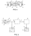
- FIG. 4 schematically shows a set of elements sensitive 41,42,43 contiguous, on which a part of fingerprint 44, the surface of which has been shown in FIG. 4 enlarged.
- the fingerprint has at this location two bumps 50 and 51 and a hollow 53.
- the bumps 50 and 51 are respectively in contact with the sensitive elements 41 and 43 while the hollow 53 is not in contact with the sensitive element 42.
- the heat flow F1 dissipated by the finger pressed on the sensor is more important on the sensitive elements 41 and 43 in contact with the respective bumps 50 and 51 that the flow of heat F2 dissipated by element sensitive 42 which is not in contact with the finger due to the presence of the hollow 53 of the fingerprint.
- a fingerprint reading system comprising means for viewing and processing fingerprint images supplied by a sensor with heating resistors and having a area of the order of magnitude of a fingerprint that we want read.
- the system includes a sensor 60, as described previously, whose sensitive elements are temporarily heated by one or more heating resistors.
- a stationary finger 62 On the pyroelectric surface sensor 60, is pressed a stationary finger 62, having an imprint digital 63.
- the sensor 60 provides an analog signal to an output 64 representing the image of the fingerprint 63.
- the output 64 of the sensor is connected on the one hand to a video frequency terminal 66 comprising a screen of visualization of the images of the imprint and on the other hand to an entry analog 68 of an analog / digital converter 70.
- Output digital 72 of converter 70 is connected to an input of a digital memory 80.
- the output of this memory is connected to a digital input 82 of a processing and calculation system, for example a microcomputer 90.
- Each analog image generated by the sensor 60 is displayed on the screen of the video frequency terminal 66, which makes it possible to judge in real time of the quality of the images constantly supplied by the sensor 60.
- Finger 62 can be moved slightly over the pyroelectric surface of the sensor in order to find the best image of fingerprint 63, the speed of movement of the finger being limited, to be compatible with the frequency of images output from the sensor.
- the image of the fingerprint is simply viewed on the video frequency terminal 66, without performing an acquisition of the image of the imprint by the system.
- the terminal videofrequency 66 includes a known adaptation system, not shown in the figure, allowing the analog signal to be output from the sensor in a video signal viewable by a screen classic video frequencies.
- the image is acquired and digitized on a number N of bits by the converter analog digital 70.
- the digitized image supplied by converter 70 is stored at a relatively high speed, on the order of a few megahertz, in digital memory 80.
- This digital memory 80 is modest in size, corresponding approximately to the product of the number of sensitive elements of the sensor by the number of bits N to code the level of each sensitive element.
- the scanned image stored in digital memory 80 is in continuation transmitted to the microcomputer 90, at a lower speed than the speed of storage in memory, of the order of a few hundred kilohertz, compatible with the input speeds allowed by the inputs digital (parallel or serial port) of the microcomputer 90.
- the system which is the subject of this invention does not require image reconstruction algorithm, however the image stored in the microcomputer 90, is first of all treated by known methods, to improve its quality and then to extract information useful to the fingerprint recognition.
- a search algorithm allows to authenticate the memorized imprint by comparing it with an image of a pre-registered fingerprint corresponding to an individual to authenticate.
- These pattern recognition algorithms can use for example, contour extraction treatments, vectorization of contours, or other types of processing, the useful image of an imprint digital is actually a set of contours corresponding to the crests and furrows of this imprint.
- For authentication we will compare the sets of contours detected to sets of contours prerecorded corresponding to an individual to be authenticated. Sets contours can then be stored in the form of vector tables describing these contours.
Abstract
Description
L'invention concerne les systèmes de lecture d'empreintes digitales, utilisés notamment dans des dispositifs d'authentification de personnes.The invention relates to fingerprint reading systems. digital, used in particular in authentication devices people.
Les nombreux systèmes d'authentification des personnes basés sur l'analyse des empreintes digitales, comportent au moins un capteur permettant d'obtenir une image de l'empreinte digitale de la personne à identifier. Dans les systèmes actuels, le doigt est posé sur le capteur dont la surface de lecture doit être nécessairement de l'ordre de grandeur du doigt. Le capteur est associé à un système d'analyse permettant de comparer l'image de l'empreinte digitale qu'il fournit, à une image d'une empreinte digitale de référence stockée sur un médium adéquat, par exemple une carte à puce.The many authentication systems based on people on fingerprint analysis, have at least one sensor providing a picture of the person's fingerprint identify. In current systems, the finger is placed on the sensor whose reading surface must necessarily be of the order of magnitude of the finger. The sensor is associated with an analysis system making it possible to compare the image of the fingerprint it provides, to an image of a fingerprint digital reference stored on a suitable medium, for example a Smartcard.
Dans la plupart des cas, les capteurs fournissent une information de type analogique et le système d'analyse fait appel à un traitement numérique de l'image de l'empreinte digitale qui doit être numérisée en sortie du capteur à l'aide d'un convertisseur analogique numérique. Dans certaines réalisations, le capteur délivre directement l'image numérisée.In most cases, the sensors provide information analog type and the analysis system calls for processing digital image of the fingerprint to be scanned in sensor output using an analog to digital converter. In in certain embodiments, the sensor directly delivers the digitized image.
Les systèmes de lecture des empreintes digitales sont souvent basés sur l'utilisation de dispositifs optiques comme par exemple une caméra vidéo captant l'image du doigt, mais une simple photographie du même doigt permet d'obtenir la même image en sortie de la caméra et ainsi de frauder le système. Pour pallier cet inconvénient, certains systèmes utilisent des prismes ou des microprismes afin de s'assurer que c'est bien un véritable doigt et non une photographie qui se trouve placé devant le capteur, la réflexion de la lumière ne s'effectuant qu'aux endroits où les sillons de l'empreinte ne touchent pas le prisme, une photographie est alors inopérante. Néanmoins les systèmes optiques ne permettent pas de déterminer si le doigt qui est placé devant le capteur est bien vivant et n'est donc pas un doigt par exemple moulé. Les systèmes optiques présentent d'autres inconvénients comme par exemple leur volume important et un coût de production élevé. Fingerprint reading systems are often based on the use of optical devices such as a video camera capturing the image of the finger, but a simple photograph of the same finger provides the same image output from the camera and so to defraud the system. To overcome this drawback, some systems use prisms or microprisms to ensure that it is real finger and not a photograph which is placed in front of the sensor, the reflection of light only taking place where the grooves of the imprint do not touch the prism, a photograph is then inoperative. However, optical systems do not allow determine if the finger in front of the sensor is alive and not therefore not a molded finger, for example. Optical systems present other disadvantages such as their large volume and cost high production.
D'autres moyens ont été proposés pour réaliser des dispositifs d'authentification de personnes par les empreintes digitales, exploitant les possibilités de traitement collectif de l'industrie du semi-conducteur, donc potentiellement moins coûteux et offrant les avantages de l'intégration du capteur et de tout ou partie de la chaíne de traitement des données du dispositif d'authentification notamment la numérisation de l'image en sortie du capteur, le stockage de l'image de référence et l'authentification. Le capteur de lecture des empreintes digitales comporte une matrice d'éléments sensibles, fournissant un signal électrique différent selon qu'une crête du sillon de l'empreinte digitale touche ou ne touche pas un élément sensible du capteur.Other means have been proposed for producing devices authentication of people by fingerprints, exploiting possibilities of collective processing of the semiconductor industry, therefore potentially less expensive and offering the advantages of integrating the sensor and all or part of the data processing chain of the authentication device, in particular the digitization of the output image of the sensor, storage of the reference image and authentication. The fingerprint reader sensor has a matrix sensitive elements, providing a different electrical signal depending on whether crest of fingerprint groove touches or does not touch an item sensitive sensor.
Des brevets ont été déposés sur différents moyens de lecture des empreintes digitales :
- le brevet US,4,353,056, décrit un principe de lecture basé sur la variation de la capacité des éléments sensibles du capteur.
- US Patent 4,353,056 describes a reading principle based on the variation of the capacity of the sensitive elements of the sensor.
D'autres systèmes comportent des capteurs ayant des composés sensibles à la pression, à la température, ou bien à la pression et à la température, transformant l'information spatiale de pression et/ou de température en un signal électrique qui est ensuite collecté par un multiplexeur à semi-conducteurs, qui peut être par exemple une matrice de transfert de charges, connue sous la dénomination anglaise de "CCD"; le brevet US,4,394,773, décrit un tel principe.Other systems include sensors with compounds sensitive to pressure, temperature, or pressure and temperature, transforming the spatial information of pressure and / or temperature into an electrical signal which is then collected by a semiconductor multiplexer, which can for example be a matrix of charge transfer, known by the English name of "CCD"; the US Patent 4,394,773 describes such a principle.
Les capteurs basés sur les effets piézo et/ou pyroélectrique sont les plus intéressants car ils sont sensibles à la pression et/ou à la chaleur exercée sur ses éléments sensibles, ce qui permet de déterminer, lors de la lecture de l'empreinte digitale, si le doigt est bien vivant par la chaleur propre qu'il dégage. Il est aussi possible de détecter les variations dues à la pulsation du sang dans le doigt, induisant une variation de chaleur et/ou de pression, ce qui permet d'obtenir une plus grande fiabilité dans l'authentification de l'empreinte digitale.Sensors based on piezo and / or pyroelectric effects are the most interesting because they are sensitive to pressure and / or heat exerted on its sensitive elements, which makes it possible to determine, during the reading of the fingerprint, if the finger is alive by the heat clean it gives off. It is also possible to detect variations due to the pulsation of blood in the finger, inducing a variation in heat and / or pressure, which allows greater reliability in fingerprint authentication.
Le signal électrique fourni par les capteurs intégrés sur un substrat semi-conducteur présente l'inconvénient d'être fugitif et un système spécifique est nécessaire pour le maintenir dans le temps car les charges électriques sont induites par des variations des effets physiques (température, pression...) sur le capteur et en conséquence le signal à sa sortie tend à disparaítre à la mise en équilibre des effets physiques. Les constantes de temps de disparition du signal sont de l'ordre de quelques millisecondes à quelques secondes dans les cas favorables.The electrical signal provided by the sensors integrated on a the semiconductor substrate has the disadvantage of being fugitive and a system specific is necessary to maintain it over time because the charges are induced by variations in physical effects (temperature, pressure ...) on the sensor and consequently the signal at its exit tends to disappear when the physical effects are balanced. The signal disappearance time constants are of the order of a few milliseconds to a few seconds in favorable cases.
Le résultat pratique est la production d'une série d'images à partir du moment où le doigt est posé sur le capteur. La qualité de contraste de ces images n'est pas stable et elles ont tendance à s'évanouir ce qui complique la tâche du système de reconnaissance car il doit alors analyser toutes les images produites en permanence par le capteur afin de trouver la plus correcte pour l'authentification.The practical result is the production of a series of images from the moment the finger is placed on the sensor. The contrast quality of these images are not stable and they tend to faint which complicates the task of the recognition system because it must then analyze all the images continuously produced by the sensor in order to find the more correct for authentication.
Des systèmes avec une excitation extérieure au capteur ont été proposés, par exemple envoi d'un faisceau d'énergie sous forme de micro-ondes, mais ils compliquent le système et augmentent son volume et son prix.Systems with excitation external to the sensor have been proposed, for example sending an energy beam in the form of microwaves, but they complicate the system and increase its volume and its price.
On peut pallier la disparition transitoire de l'image de l'empreinte à l'aide d'une mémoire électronique mais ceci complique la conception du capteur et augmente son coût de fabrication car cela requiert une technologie permettant de réaliser cette mémorisation et il est très difficile de construire un système suffisamment précis, fiable et peu coûteux capable de décider quelle est la meilleure image parmi toutes celles produites par le capteur.We can compensate for the transitory disappearance of the image of the imprint using an electronic memory but this complicates the design of the sensor and increases its manufacturing cost because it requires technology to achieve this memorization and it is very difficult to build a sufficiently precise, reliable and inexpensive system capable to decide which is the best image among all those produced by the sensor.
La présente invention propose de pallier les inconvénients de l'art antérieur en proposant un système de lecture d'empreintes digitales comportant un capteur ayant une matrice d'éléments sensibles et un multiplexeur permettant de mesurer individuellement des charges électriques engendrées par un phénomène transitoire dans les éléments sensibles de la matrice, la matrice étant encapsulée dans un boítier ouvert sur une de ses faces pour permettre d'appuyer un doigt sur la matrice, la matrice fournissant des signaux électriques correspondant à un motif matriciel constituant une image globale de l'empreinte digitale, caractérisé en ce que le capteur comporte des moyens pour créer une variation thermique interne transitoire de la matrice d'éléments sensibles, le système comprenant des moyens pour lire les signaux de la matrice après application de cette variation thermique.The present invention proposes to overcome the drawbacks of the art by proposing a fingerprint reading system comprising a sensor having a matrix of sensitive elements and a multiplexer for individually measuring loads electrics generated by a transient phenomenon in the elements sensitive to the matrix, the matrix being encapsulated in an open case on one of its faces to allow a finger to be pressed on the matrix, the matrix providing electrical signals corresponding to a pattern matrix constituting a global image of the fingerprint, characterized in that the sensor includes means for creating a variation transient internal thermal of the matrix of sensitive elements, the system comprising means for reading the signals from the matrix after application of this thermal variation.
Cette variation de température locale du capteur, a pour effet de créer une charge locale dans le matériau pyroélectrique du capteur. This variation in local temperature of the sensor has the effect of create a local charge in the pyroelectric material of the sensor.
Une empreinte digitale se présente sous la forme d'un ensemble de sillons de la peau, comportant des lignes de bosses et de creux. Lorsque la zone du doigt comportant cette empreinte est appuyée sur la matrice d'éléments sensibles échauffés du capteur, la présence des bosses de l'empreinte digitale en contact avec des éléments sensibles conduit à une meilleure dissipation de la chaleur de ces éléments que la présence des creux de cette même empreinte.A fingerprint is in the form of a set of skin grooves, with lines of bumps and hollows. When the area of the finger with this imprint is pressed on the matrix sensitive heated elements of the sensor, the presence of bumps in the the fingerprint in contact with sensitive elements leads to a better heat dissipation of these elements than the presence of hollow of this same imprint.
La dissipation de cette chaleur et en conséquence la variation de température de chaque élément sensible est donc plus ou moins importante selon la présence, sur ces éléments sensibles du capteur, des bosses ou des creux de l'empreinte digitale. Ce phénomène crée une modulation spatiale des variations thermiques dans la couche pyroélectrique et en conséquence une modulation spatiale des charges collectées par le multiplexeur. Le doigt étant immobile, et la lecture des charges étant effectuée sequentiellement, se traduit par la production par le système de lecture d'une image stable. L'élévation de température de la couche pyroélectrique reste faible, inférieure à environ un degré Kelvin.The dissipation of this heat and consequently the variation of temperature of each sensitive element is therefore more or less important depending on the presence, on these sensitive elements of the sensor, of bumps or fingerprint troughs. This phenomenon creates modulation spatial thermal variations in the pyroelectric layer and in consequently a spatial modulation of the charges collected by the multiplexer. The finger being stationary, and the reading of the charges being carried out sequentially, results in the production by the system of reading a stable image. Layer temperature rise pyroelectric remains low, less than about one Kelvin degree.
La variation locale transitoire de température des éléments sensibles est réalisée par une résistance chauffante placée au contact de la matrice d'éléments sensibles, parcourue par un courant transitoire de chauffage du capteur fonctionnant en synchronisme avec la lecture des charges par le multiplexeur. Ce courant transitoire fait monter la température localement par dissipation de l'énergie électrique par effet Joule.The transient local temperature variation of the elements sensitive is achieved by a heating resistor placed in contact with the matrix of sensitive elements, traversed by a transient current of heating of the sensor operating in synchronism with the reading of loads by the multiplexer. This transient current increases the temperature locally by dissipation of electrical energy by Joule effect.
Dans une première réalisation, la matrice d'éléments sensibles est organisée en lignes et le capteur comporte alors autant de résistances chauffantes que de lignes d'éléments sensibles. Chaque résistance chauffante, associée à sa ligne respective, est parallèle à cette ligne pour effectuer son chauffage. Le multiplexeur effectue ligne par ligne, la lecture des charges des éléments sensibles, chaque ligne étant successivement lue et remise à zéro une par une. Le courant de chauffage est injecté dans chaque résistance associée à une ligne, par exemple, juste après la lecture de la ligne, ou pendant la remise à zéro des charges électriques des capacités pyroélectriques. L'image de l'empreinte digitale complète est reconstituée par le système. In a first embodiment, the matrix of sensitive elements is organized in lines and the sensor then has as many resistors heating only lines of sensitive elements. Each resistance heater, associated with its respective line, is parallel to this line for heat it. The multiplexer performs line by line, reading loads of sensitive elements, each line being successively read and reset one by one. The heating current is injected into each resistance associated with a line, for example, just after reading of the line, or during the resetting of the electrical charges of the pyroelectric capacities. The image of the full fingerprint is reconstituted by the system.
Dans une autre réalisation une seule résistance chauffante est utilisée pour chauffer l'ensemble des éléments sensibles de la matrice. Cette unique résistance sous la forme d'un serpentin, parcourt toute la surface du capteur en passant entre les éléments sensibles afin effectuer leur chauffage. Après injection du courant dans la résistance, les charges des capacités des éléments sensibles représentent l'image complète de l'empreinte digitale. Cette image est figée par une mémorisation de la charge créée dans chaque élément sensible de la matrice puis l'image est lue séquentiellement pour reconstituer l'image complète de l'empreinte. Le courant peut être injecté dans la résistance, par exemple, pendant la lecture séquentielle de l'image.In another embodiment, only one heating resistance is used to heat all the sensitive elements of the matrix. This unique resistance in the form of a serpentine, covers the entire surface of the sensor passing between the sensitive elements in order to perform their heater. After injecting the current into the resistor, the charges of capabilities of sensitive elements represent the full picture of the fingerprint. This image is frozen by a memorization of the charge created in each sensitive element of the matrix then the image is read sequentially to reconstruct the complete image of the imprint. The current can be injected into the resistor, for example, during reading sequential of the image.
On peut envisager aussi que la lecture des éléments sensibles se fasse élément par élément, ce qui nécessite un adressage à la fois en ligne et en colonne et une résistance par élément.We can also consider that the reading of sensitive elements do element by element, which requires addressing both online and in column and one resistance per element.
Un autre aspect de cette invention réside dans la possibilité d'effectuer un test automatique du bon fonctionnement de chaque élément sensible de la matrice sans utiliser par exemple des sources de température et/ou de pression externes au système, appliquées au capteur. En effet le chauffage transitoire des éléments sensibles du capteur par la résistance ou les résistances intégrées au capteur, crée des charges fugitives dans les capacités des éléments sensibles qui permettent de vérifier par le contrôle de ces charges, le bon fonctionnement de chaque élément sensible de la matrice.Another aspect of this invention is the possibility to perform an automatic test of the proper functioning of each element sensitive of the matrix without using for example temperature sources and / or pressure external to the system, applied to the sensor. Indeed the transient heating of sensitive sensor elements by the resistance or the resistors built into the sensor, creates fugitive charges in the capabilities of sensitive elements that allow verification by control of these charges, the proper functioning of each sensitive element of the matrix.
D'autres caractéristiques de l'invention apparaítront à la lecture de la description détaillée des réalisations suivantes et qui est faite en référence aux dessins annexés dans lesquels :
- la figure 1 représente une vue générale du capteur d'empreinte,
- la figure 2 représente une coupe schématique montrant la constitution du capteur dans la zone d'un élément sensible,
- la figure 3 montre un exemple de réalisation des résistances chauffantes,
- la figure 4 montre la dissipation thermique des éléments sensibles par l'empreinte digitale,
- la figure 5 représente un synoptique d'un système de lecture d'empreintes digitales selon l'invention.
- FIG. 1 represents a general view of the fingerprint sensor,
- FIG. 2 represents a schematic section showing the constitution of the sensor in the area of a sensitive element,
- FIG. 3 shows an exemplary embodiment of the heating resistors,
- FIG. 4 shows the thermal dissipation of sensitive elements by the fingerprint,
- FIG. 5 represents a block diagram of a system for reading fingerprints according to the invention.
La figure 1, montre une vue générale du capteur d'empreintes
digitales comportant des résistances chauffantes. Le capteur d'empreinte 10,
est un circuit intégré ayant une forme rectangulaire de taille suffisante pour
effectuer la lecture de l'empreinte digitale. Le circuit intégré comporte une
matrice d'éléments sensibles réalisés par une couche active pyroélectrique
placée entre une électrode supérieure et un réseau matriciel d'électrodes
inférieures. Les électrodes inférieures reposent sur un substrat semi-conducteur
dans lequel est formé un circuit électronique intégré apte à
traiter les charges électriques engendrées par la couche pyroélectrique sur
chacune des électrodes du réseau. Le circuit intégré est contenu dans un
support 13 relié par des broches de connexion 14 qui transmettent à
l'extérieur du capteur des signaux électriques dont l'ensemble représente
une image à un moment donné, du motif de température de la couche active
pyroélectrique. La constitution des électrodes inférieures en réseau
matriciel permet de réaliser un réseau d'éléments sensibles pyroélectriques
individuels même si la couche pyroélectrique est continue.Figure 1 shows a general view of the fingerprint sensor
digital with heating resistors. The
La figure 2 représente schématiquement une partie d'un circuit
intégré 20 dans la zone d'un élément sensible du capteur comportant à
proximité une résistance chauffante 29.Figure 2 schematically represents part of a circuit
integrated 20 into the area of a sensitive element of the sensor comprising
near a
Le circuit intégré comporte :
un substrat semi-conducteur 22, qui est en principe un substrat de silicium. Dans ce substrat sont formés des circuits de lecture et de traitement de charges électriques constituant le multiplexeur 23. Ces circuits sont par exemple des circuits CCD (circuits à transfert de charges), ou des circuits C-MOS. Ils sont réalisés selon les technologies courantes de fabrication de circuits intégrés au silicium. Les circuits sont constitués en réseau, en fonction du motif matriciel d'éléments pyroélectriques qui sera formé ultérieurement.un isolant thermique 24, déposé sur le substrat- des capacités pyroélectriques constituées par une armature
métallique inférieure 26 et une armature métallique supérieure 27, entre
lesquels est située une couche 28 de matériau pyroélectrique. L'armature
métallique supérieure 27 est commune à l'ensemble des capacités des
éléments sensibles et peut être trouée (réticulée) afin de limiter la
propagation latérale de la chaleur. L'armature métallique inférieure 26 est
reliée à un accès 38 du multiplexeur 23, effectuant la lecture des charges
des capacités. La résistance chauffante 29 est réalisée au même niveau que
l'électrode inférieure 26 et se trouve reliée,
par un accès 30, à un générateur de courant transitoire, du multiplexeur 23. - une fine couche de
protection 32, déposée sur les éléments sensibles, dont la propagation thermique doit être essentiellement perpendiculaire au plan du capteur, afin de limiter la diffusion latérale de la chaleur.
- a
semiconductor substrate 22, which is in principle a silicon substrate. In this substrate are formed circuits for reading and processing electrical charges constituting themultiplexer 23. These circuits are for example CCD circuits (charge transfer circuits), or C-MOS circuits. They are made using current technologies for manufacturing integrated circuits with silicon. The circuits are networked, according to the matrix pattern of pyroelectric elements which will be formed later. - a
thermal insulator 24, deposited on the substrate - pyroelectric capacitors constituted by a
lower metal frame 26 and anupper metal frame 27, between which is located alayer 28 of pyroelectric material. Theupper metal frame 27 is common to all of the capacities of the sensitive elements and can be perforated (crosslinked) in order to limit the lateral propagation of heat. Thelower metal frame 26 is connected to anaccess 38 of themultiplexer 23, reading the loads from the capacities. Theheating resistor 29 is produced at the same level as thelower electrode 26 and is connected, by anaccess 30, to a transient current generator, of themultiplexer 23. - a thin
protective layer 32, deposited on the sensitive elements, the thermal propagation of which must be essentially perpendicular to the plane of the sensor, in order to limit the lateral diffusion of the heat.
Le matériau de la couche pyroélectrique peut être par exemple un polyfluorure de vinylidène (PVDF), un polyfluorure de vinylidène-trifluoroéthylène (PVDF-TrFE), un polycyanure de vinylidène-vinylacétate (PVDCN-VAc), un polycyanure de vinylidène-fluorure de vinylidène (PVDCN-VDF). D'autres couches sensibles sont possibles, en particulier toutes celles qui produisent des charges électriques en fonction d'un paramètre pyro-piézoélectrique.The material of the pyroelectric layer may for example be a polyvinylidene fluoride (PVDF), a polyvinylidene-trifluoroethylene fluoride (PVDF-TrFE), a polyvinylidene-vinyl acetate (PVDCN-VAc), a polyvinylidene-vinylidene fluoride (PVDCN-VDF). Other sensitive layers are possible, in particular all those which produce electric charges according to a pyro-piezoelectric parameter.
Dans le cas des copolymères précédemment cités, le principal effet utilisé est la génération des charges électriques induites par la variation de température du copolymère.In the case of the abovementioned copolymers, the main effect used is the generation of electrical charges induced by the variation temperature of the copolymer.
La figure 3, montre une vue partielle d'un circuit intégré 35 au
niveau du plan des armatures inférieures 36 des capacités pyroélectriques
et des résistances de chauffage 37, situées sur le même plan du circuit
intégré. Les résistances de chauffage 37, parcourent le circuit intégré, entre
des lignes, d'axe XX', d'armatures inférieures des capacités pyroélectriques
et parallèlement à ces lignes. Les résistances chauffantes 37 sont réalisées
par dépôt, par exemple de titane, au même moment que les armatures
métalliques inférieures 36 des capacités pyroélectriques.FIG. 3 shows a partial view of an
Dans le cas de lecture ligne par ligne, une résistance est associée à une ligne d'éléments sensibles. Dans le cas de lecture d'une image complète une seule résistance est associée à l'ensemble des éléments sensibles du capteur.In the case of line-by-line reading, a resistance is associated with a line of sensitive elements. In the case of reading a complete image a single resistance is associated with all of the sensitive elements of the sensor.
La figure 4, montre schématiquement un ensemble d'éléments
sensibles 41,42,43 contigus, sur lesquels est appuyés une partie de
l'empreinte digitale 44 dont on a représenté sur la figure 4 la surface
agrandie. L'empreinte digitale, comporte à cet endroit deux bosses 50 et 51
et un creux 53. Les bosses 50 et 51 sont respectivement en contact avec
les éléments sensibles 41 et 43 alors que le creux 53 n'est pas en contact
avec l'élément sensible 42. Lors de l'échauffement transitoire des éléments
sensibles, le flux de chaleur F1 dissipé par le doigt appuyé sur le capteur est
plus important sur les éléments sensibles 41 et 43 en contact avec les
bosses respectives 50 et 51 que le flux de chaleur F2 dissipée par élément
sensible 42 qui n'est pas en contact avec le doigt du à la présence du creux
53 de l'empreinte digitale. Cela crée lors de la variation thermique
transitoire produite par le passage du courant dans la résistance de
chauffage une variation spatiale de température des éléments sensibles et
en conséquence une variation spatiale, image de la variation thermique, des
charges dans les capacités pyroélectriques.Figure 4 schematically shows a set of elements
sensitive 41,42,43 contiguous, on which a part of
Nous allons décrire par la suite un exemple de réalisation d'un système de lecture d' empreintes digitales, selon l'invention, comportant des moyens de visualisation et de traitement des images d'empreintes digitales fournies par un capteur avec des résistances chauffantes et ayant une surface de l'ordre de grandeur d'une empreinte digitale dont on veut effectuer la lecture.We will describe below an embodiment of a fingerprint reading system according to the invention, comprising means for viewing and processing fingerprint images supplied by a sensor with heating resistors and having a area of the order of magnitude of a fingerprint that we want read.
Le système comporte un capteur 60, tel qu'il a été décrit
précédemment, dont les éléments sensibles sont chauffés transitoirement
par une ou plusieurs résistances chauffantes. Sur la surface pyroélectrique
du capteur 60, est appuyé un doigt 62 immobile, ayant une empreinte
digitale 63. Le capteur 60 fournit à une sortie 64, un signal analogique
représentant l'image de l'empreinte digitale 63. La sortie 64 du capteur est
connectée d'une part à un terminal vidéofréquences 66 comportant un écran
de visualisation des images de l'empreinte et d'autre part à une entrée
analogique 68 d'un convertisseur 70 analogique/numérique. Une sortie
numérique 72 du convertisseur 70 est connectée à une entrée d'une
mémoire numérique 80. La sortie de cette mémoire est connectée à une
entrée numérique 82 d'un système de traitement et de calcul, par exemple
un micro-ordinateur 90.The system includes a
Chaque image analogique générée par le capteur 60 est
visualisée sur l'écran du terminal vidéofréquence 66, ce qui permet de juger
en temps réel de la qualité des images fournies constamment par le capteur
60. Le doigt 62 peut être déplacé légèrement sur la surface pyroélectrique
du capteur afin de trouver la meilleure image de l'empreinte digitale 63, la
vitesse de déplacement du doigt étant limitée, pour être compatible avec la
fréquence des images en sortie du capteur.Each analog image generated by the
Dans cette première phase, l'image de l'empreinte digitale est
simplement visualisée sur le terminal vidéofréquences 66, sans effectuer
une acquisition de l'image de l'empreinte par le système. Le terminal
vidéofréquence 66 comporte un système d'adaptation connu, non représenté
sur la figure, permettant de transformer le signal analogique en sortie du
capteur en un signal vidéofréquences visualisable par un écran
vidéofréquences classique.In this first phase, the image of the fingerprint is
simply viewed on the
Lorsque l'image est considérée comme satisfaisante, l'image est
acquise et numérisée sur un nombre N de bits par le convertisseur
analogique numérique 70. L'image numérisée fournie par le convertisseur 70
est stockée à une vitesse relativement élevée, de l'ordre de quelques
mégahertzs, dans la mémoire numérique 80. Cette mémoire numérique 80
est de taille modeste, correspondant environ au produit du nombre
d'éléments sensibles du capteur par le nombre de bits N pour coder le
niveau de chaque élément sensible.When the image is considered satisfactory, the image is
acquired and digitized on a number N of bits by the converter
analog digital 70. The digitized image supplied by
L'image numérisée stockée dans la mémoire numérique 80 est en
suite transmise au micro-ordinateur 90, à une vitesse plus faible que la
vitesse de stockage dans la mémoire, de l'ordre de quelques centaines de
kilohertz, compatible avec les vitesses d'entrée admises par les entrées
numériques (port parallèle ou port série) du micro-ordinateur 90.The scanned image stored in
Le système faisant l'objet de cette invention, ne nécessite pas
d'algorithme de reconstruction d'images, cependant l'image stockée dans le
micro-ordinateur 90, est tout d'abord traitée par des méthodes connues, pour
améliorer sa qualité et ensuite pour extraire l'information utile à la
reconnaissance de l'empreinte digitale. Un algorithme de recherche permet
d'authentifier l'empreinte mémorisée en la comparant avec une image
d'empreinte digitale préenregistrée correspondant à un individu à
authentifier. Ces algorithmes de reconnaissances de formes peuvent utiliser
par exemple des traitements d'extraction de contours, de vectorisation des
contours, ou autres types de traitements, l'image utile d'une empreinte
digitale est en fait un ensemble de contours correspondant aux crêtes et aux
sillons de cette empreinte. Pour l'authentification, on comparera les
ensembles des contours détectés à des ensembles de contours
préenregistrés correspondant à un individu à authentifier. Les ensembles
des contours pourront alors être stockées sous formes de tables de vecteurs
décrivant ces contours.The system which is the subject of this invention does not require
image reconstruction algorithm, however the image stored in the
Claims (11)
Applications Claiming Priority (2)
| Application Number | Priority Date | Filing Date | Title |
|---|---|---|---|
| FR9613453A FR2755526B1 (en) | 1996-11-05 | 1996-11-05 | FINGERPRINT READING SYSTEM WITH INTEGRATED HEATING RESISTORS |
| FR9613453 | 1996-11-05 |
Publications (1)
| Publication Number | Publication Date |
|---|---|
| EP0840250A1 true EP0840250A1 (en) | 1998-05-06 |
Family
ID=9497327
Family Applications (1)
| Application Number | Title | Priority Date | Filing Date |
|---|---|---|---|
| EP97402556A Withdrawn EP0840250A1 (en) | 1996-11-05 | 1997-10-28 | System for reading fingerprints with integrated heating resistances |
Country Status (5)
| Country | Link |
|---|---|
| US (1) | US6061464A (en) |
| EP (1) | EP0840250A1 (en) |
| JP (1) | JP4048246B2 (en) |
| CA (1) | CA2217779A1 (en) |
| FR (1) | FR2755526B1 (en) |
Cited By (11)
| Publication number | Priority date | Publication date | Assignee | Title |
|---|---|---|---|---|
| US6633656B1 (en) | 1999-12-24 | 2003-10-14 | Institut National D'optique | Microthermistor based fingerprint sensor |
| EP2385486A1 (en) * | 2010-05-06 | 2011-11-09 | Commissariat à l'Énergie Atomique et aux Énergies Alternatives | Transducer for temporal variation of temperature, electronic chip including transducteur and method for manufacturing chip |
| GB2481779A (en) * | 2010-01-20 | 2012-01-11 | I Evo Ltd | A biometric reading device with a heater |
| FR3044409A1 (en) * | 2015-11-30 | 2017-06-02 | Commissariat Energie Atomique | THERMAL PATTERN SENSOR COMPRISING A HIGH PYROELECTRIC PORTION WITH HIGH THERMAL CONDUCTIVITY |
| WO2017144455A1 (en) * | 2016-02-22 | 2017-08-31 | Commissariat A L'energie Atomique Et Aux Energies Alternatives | Sensor of thermal patterns with thermo-resistive capsules |
| EP3276585A1 (en) * | 2016-07-29 | 2018-01-31 | Commissariat à l'énergie atomique et aux énergies alternatives | Active thermal sensor adapted to large pixels |
| EP3276534A1 (en) * | 2016-07-29 | 2018-01-31 | Commissariat à l'énergie atomique et aux énergies alternatives | Method for capturing a thermal pattern with optimised heating of pixels |
| WO2018020176A1 (en) * | 2016-07-29 | 2018-02-01 | Commissariat A L'energie Atomique Et Aux Energies Alternatives | Active thermal pattern sensor comprising a passive matrix of pixels |
| CN108664856A (en) * | 2017-03-31 | 2018-10-16 | 奇景光电股份有限公司 | Fingerprint sensing circuit, the processing method of fingerprint image and electronic device |
| EP3483787A1 (en) * | 2017-11-13 | 2019-05-15 | Commissariat à l'énergie atomique et aux énergies alternatives | Method for making a stack of layers for a thermal matrix sensor |
| EP3767261A1 (en) * | 2019-07-18 | 2021-01-20 | Idemia Identity & Security France | Pixel matrix of a thermal pattern sensor, associated sensor with heating lines in coil |
Families Citing this family (46)
| Publication number | Priority date | Publication date | Assignee | Title |
|---|---|---|---|---|
| CA2371998C (en) * | 1999-02-11 | 2006-01-24 | British Telecommunications Public Limited Company | Analysis of video signal quality |
| JP4578041B2 (en) * | 1999-08-09 | 2010-11-10 | ソナベーション, インコーポレイテッド | Piezoelectric fingerprint scanner |
| US6284561B1 (en) * | 1999-10-08 | 2001-09-04 | United Microelectronics Corp. | Method of forming a metal plate of a fingerprint sensor chip on a semiconductor wafer |
| US20040207606A1 (en) * | 1999-11-08 | 2004-10-21 | Atwood Stephen P. | Sensing the size of a touch point in a touch-sensitive panel employing resistive membranes |
| KR20010046215A (en) * | 1999-11-11 | 2001-06-05 | 김상균 | Thermal Semiconductor Fingerprint Sensor, Fingerprint Sensing Device Using Thermal Fingerprint Sensor, Manufacturing Method thereof, and Fingerprint Recognizing Method thereof |
| EP1266346B1 (en) | 2000-03-23 | 2009-04-29 | Cross Match Technologies, Inc. | Piezoelectric biometric identification device and applications thereof |
| US7067962B2 (en) | 2000-03-23 | 2006-06-27 | Cross Match Technologies, Inc. | Multiplexer for a piezo ceramic identification device |
| US20030001459A1 (en) * | 2000-03-23 | 2003-01-02 | Cross Match Technologies, Inc. | Secure wireless sales transaction using print information to verify a purchaser's identity |
| JP3559754B2 (en) | 2000-07-25 | 2004-09-02 | Necエレクトロニクス株式会社 | Fingerprint authentication device |
| AU2002305257A1 (en) | 2001-04-27 | 2002-11-11 | Atrua Technologies, Inc. | Capacitive sensor system with improved capacitance measuring sensitivity |
| US7259573B2 (en) | 2001-05-22 | 2007-08-21 | Atrua Technologies, Inc. | Surface capacitance sensor system using buried stimulus electrode |
| US20030013328A1 (en) * | 2001-05-22 | 2003-01-16 | Andrade Thomas L. | Connection assembly for integrated circuit sensors |
| US6657358B2 (en) * | 2001-06-26 | 2003-12-02 | Hewlett-Packard Development Company, L.P. | Power supply including pyroelectric capacitor |
| US6707093B2 (en) | 2001-11-30 | 2004-03-16 | Stmicroelectronics, Inc. | Selective ionic implantation of fluoropolymer film to modify the sensitivity of underlying sensing capacitors |
| US6762470B2 (en) | 2001-11-30 | 2004-07-13 | Stmicroelectronics, Inc. | Fingerprint sensor having a portion of the fluorocarbon polymer physical interface layer amorphized |
| US20030104693A1 (en) * | 2001-11-30 | 2003-06-05 | Siegel Harry M. | Use of fluoropolymer coating for planarizing and passivating integrated circuit devices |
| DE10222616A1 (en) * | 2002-05-17 | 2003-12-04 | Univ Albert Ludwigs Freiburg | Fingerprint verification module |
| KR20030093841A (en) * | 2002-06-05 | 2003-12-11 | 주식회사 카로스기술 | System and Method of Finger-print Recognition |
| US20040104807A1 (en) * | 2002-10-16 | 2004-06-03 | Frank Ko | Networked fingerprint authentication system and method |
| US6966693B2 (en) * | 2003-01-14 | 2005-11-22 | Hewlett-Packard Development Company, L.P. | Thermal characterization chip |
| JP4314843B2 (en) * | 2003-03-05 | 2009-08-19 | カシオ計算機株式会社 | Image reading apparatus and personal authentication system |
| US7474772B2 (en) | 2003-06-25 | 2009-01-06 | Atrua Technologies, Inc. | System and method for a miniature user input device |
| US7587072B2 (en) | 2003-08-22 | 2009-09-08 | Authentec, Inc. | System for and method of generating rotational inputs |
| JP2005173930A (en) * | 2003-12-10 | 2005-06-30 | Sony Corp | Electronic equipment and authentication method |
| US7697729B2 (en) | 2004-01-29 | 2010-04-13 | Authentec, Inc. | System for and method of finger initiated actions |
| GB0410201D0 (en) * | 2004-05-07 | 2004-06-09 | Yarg Biometrics Ltd | User identification system |
| JP3931898B2 (en) * | 2004-09-30 | 2007-06-20 | セイコーエプソン株式会社 | Personal authentication device |
| US7831070B1 (en) | 2005-02-18 | 2010-11-09 | Authentec, Inc. | Dynamic finger detection mechanism for a fingerprint sensor |
| US7862776B2 (en) * | 2006-01-06 | 2011-01-04 | Redxdefense, Llc | Interactive security screening system |
| US7849312B2 (en) * | 2006-03-24 | 2010-12-07 | Atmel Corporation | Method and system for secure external TPM password generation and use |
| US20070237366A1 (en) * | 2006-03-24 | 2007-10-11 | Atmel Corporation | Secure biometric processing system and method of use |
| US20080061927A1 (en) * | 2006-08-22 | 2008-03-13 | Russell Hurbert Manton | Biometric lockset |
| US8073204B2 (en) * | 2007-12-31 | 2011-12-06 | Authentec, Inc. | Hybrid multi-sensor biometric identification device |
| US8582837B2 (en) * | 2007-12-31 | 2013-11-12 | Authentec, Inc. | Pseudo-translucent integrated circuit package |
| US8791792B2 (en) | 2010-01-15 | 2014-07-29 | Idex Asa | Electronic imager using an impedance sensor grid array mounted on or about a switch and method of making |
| US8421890B2 (en) | 2010-01-15 | 2013-04-16 | Picofield Technologies, Inc. | Electronic imager using an impedance sensor grid array and method of making |
| US8866347B2 (en) | 2010-01-15 | 2014-10-21 | Idex Asa | Biometric image sensing |
| US8471345B2 (en) * | 2010-03-05 | 2013-06-25 | Authentec, Inc. | Biometric sensor assembly with integrated visual indicator |
| US8378508B2 (en) | 2010-03-05 | 2013-02-19 | Authentec, Inc. | Integrally molded die and bezel structure for fingerprint sensors and the like |
| US20130279769A1 (en) | 2012-04-10 | 2013-10-24 | Picofield Technologies Inc. | Biometric Sensing |
| FR3022663A1 (en) | 2014-06-23 | 2015-12-25 | Thomas Heron | IDENTIFICATION SYSTEM |
| FR3044443B1 (en) * | 2015-11-30 | 2018-12-07 | Commissariat A L'energie Atomique Et Aux Energies Alternatives | METHOD OF CAPTURING THERMAL PATTERN |
| CN106098736B (en) * | 2016-06-28 | 2019-05-21 | 京东方科技集团股份有限公司 | Organic Electricity laser display substrate, display panel and display device |
| FR3063163B1 (en) * | 2017-02-21 | 2021-10-08 | Commissariat Energie Atomique | GALLIUM NITRIDE LED FOOTPRINT SENSOR. |
| FR3069354B1 (en) * | 2017-07-24 | 2019-08-30 | Commissariat A L'energie Atomique Et Aux Energies Alternatives | THERMAL SENSOR WITH TWO OVERLAY PYROELECTRIC PORTIONS FOR MEASURING A DIFFERENTIAL LOAD |
| CN109376685A (en) * | 2018-11-13 | 2019-02-22 | 武汉华星光电半导体显示技术有限公司 | The manufacturing method of fingerprint identification device, fingerprint identification method and fingerprint identification device |
Citations (1)
| Publication number | Priority date | Publication date | Assignee | Title |
|---|---|---|---|---|
| FR2674051A1 (en) * | 1991-03-14 | 1992-09-18 | Gemplus Card Int | Device for identifying a person, especially by fingerprint detection |
Family Cites Families (7)
| Publication number | Priority date | Publication date | Assignee | Title |
|---|---|---|---|---|
| US4358677A (en) * | 1980-05-22 | 1982-11-09 | Siemens Corporation | Transducer for fingerprints and apparatus for analyzing fingerprints |
| US4353056A (en) * | 1980-06-05 | 1982-10-05 | Siemens Corporation | Capacitive fingerprint sensor |
| US4394773A (en) * | 1980-07-21 | 1983-07-19 | Siemens Corporation | Fingerprint sensor |
| SE425704B (en) * | 1981-03-18 | 1982-10-25 | Loefberg Bo | DATABERARE |
| US4429413A (en) * | 1981-07-30 | 1984-01-31 | Siemens Corporation | Fingerprint sensor |
| US4577345A (en) * | 1984-04-05 | 1986-03-18 | Igor Abramov | Fingerprint sensor |
| NO951427D0 (en) * | 1995-04-11 | 1995-04-11 | Ngoc Minh Dinh | Method and apparatus for measuring patterns in a partially heat conducting surface |
-
1996
- 1996-11-05 FR FR9613453A patent/FR2755526B1/en not_active Expired - Fee Related
-
1997
- 1997-10-28 EP EP97402556A patent/EP0840250A1/en not_active Withdrawn
- 1997-10-29 US US08/960,360 patent/US6061464A/en not_active Expired - Fee Related
- 1997-10-29 CA CA002217779A patent/CA2217779A1/en not_active Abandoned
- 1997-11-05 JP JP30295697A patent/JP4048246B2/en not_active Expired - Fee Related
Patent Citations (1)
| Publication number | Priority date | Publication date | Assignee | Title |
|---|---|---|---|---|
| FR2674051A1 (en) * | 1991-03-14 | 1992-09-18 | Gemplus Card Int | Device for identifying a person, especially by fingerprint detection |
Cited By (22)
| Publication number | Priority date | Publication date | Assignee | Title |
|---|---|---|---|---|
| US6633656B1 (en) | 1999-12-24 | 2003-10-14 | Institut National D'optique | Microthermistor based fingerprint sensor |
| GB2481779A (en) * | 2010-01-20 | 2012-01-11 | I Evo Ltd | A biometric reading device with a heater |
| EP2385486A1 (en) * | 2010-05-06 | 2011-11-09 | Commissariat à l'Énergie Atomique et aux Énergies Alternatives | Transducer for temporal variation of temperature, electronic chip including transducteur and method for manufacturing chip |
| FR2959657A1 (en) * | 2010-05-06 | 2011-11-11 | Commissariat Energie Atomique | TIME TEMPERATURE VARIATION TRANSDUCER, ELECTRONIC CHIP INCORPORATING THE TRANSDUCER, AND METHOD OF MANUFACTURING THE SAME |
| US8801274B2 (en) | 2010-05-06 | 2014-08-12 | Commissariat A L'energie Atomique Et Aux Energies Alternatives | Time-related temperature variation transducer, electronic chip incorporating this transducer and method of fabrication of this chip |
| FR3044409A1 (en) * | 2015-11-30 | 2017-06-02 | Commissariat Energie Atomique | THERMAL PATTERN SENSOR COMPRISING A HIGH PYROELECTRIC PORTION WITH HIGH THERMAL CONDUCTIVITY |
| WO2017093252A1 (en) * | 2015-11-30 | 2017-06-08 | Commissariat A L'energie Atomique Et Aux Energies Alternatives | Thermal pattern sensor comprising an upper pyroelectric portion with high thermal conductivity |
| WO2017144455A1 (en) * | 2016-02-22 | 2017-08-31 | Commissariat A L'energie Atomique Et Aux Energies Alternatives | Sensor of thermal patterns with thermo-resistive capsules |
| WO2018020176A1 (en) * | 2016-07-29 | 2018-02-01 | Commissariat A L'energie Atomique Et Aux Energies Alternatives | Active thermal pattern sensor comprising a passive matrix of pixels |
| EP3654242A1 (en) * | 2016-07-29 | 2020-05-20 | Commissariat à l'Energie Atomique et aux Energies Alternatives | Active thermal pattern sensor comprising a passive array of pixels |
| EP3276585A1 (en) * | 2016-07-29 | 2018-01-31 | Commissariat à l'énergie atomique et aux énergies alternatives | Active thermal sensor adapted to large pixels |
| FR3054698A1 (en) * | 2016-07-29 | 2018-02-02 | Commissariat Energie Atomique | ACTIVE THERMAL PATTERN SENSOR COMPRISING A PASSIVE MATRIX OF PIXELS |
| FR3054711A1 (en) * | 2016-07-29 | 2018-02-02 | Commissariat A L'energie Atomique Et Aux Energies Alternatives | ACTIVE THERMAL PATTERN SENSOR ADAPTED FOR LARGE PIXELS |
| FR3054697A1 (en) * | 2016-07-29 | 2018-02-02 | Commissariat A L'energie Atomique Et Aux Energies Alternatives | METHOD OF CAPTURING THERMAL PATTERN WITH OPTIMIZED HEATING OF PIXELS |
| EP3276534A1 (en) * | 2016-07-29 | 2018-01-31 | Commissariat à l'énergie atomique et aux énergies alternatives | Method for capturing a thermal pattern with optimised heating of pixels |
| US10867152B2 (en) | 2016-07-29 | 2020-12-15 | Commissariat à l'énergie atomique et aux énergies alternatives | Active thermal pattern sensor comprising a passive matrix of pixels |
| US10474864B2 (en) | 2016-07-29 | 2019-11-12 | Commissariat A L'energie Atomique Et Aux Energies Alternatives | Method of capturing thermal pattern with optimised heating of pixels |
| CN108664856A (en) * | 2017-03-31 | 2018-10-16 | 奇景光电股份有限公司 | Fingerprint sensing circuit, the processing method of fingerprint image and electronic device |
| EP3483787A1 (en) * | 2017-11-13 | 2019-05-15 | Commissariat à l'énergie atomique et aux énergies alternatives | Method for making a stack of layers for a thermal matrix sensor |
| US10580956B2 (en) | 2017-11-13 | 2020-03-03 | Commissariat A L'energie Atomique Et Aux Energies Alternatives | Method for producing a stack of layers for a matrix thermal sensor |
| FR3073651A1 (en) * | 2017-11-13 | 2019-05-17 | Commissariat A L'energie Atomique Et Aux Energies Alternatives | METHOD FOR MAKING A LAYER STACK FOR A MATRIX THERMAL SENSOR |
| EP3767261A1 (en) * | 2019-07-18 | 2021-01-20 | Idemia Identity & Security France | Pixel matrix of a thermal pattern sensor, associated sensor with heating lines in coil |
Also Published As
| Publication number | Publication date |
|---|---|
| JP4048246B2 (en) | 2008-02-20 |
| FR2755526A1 (en) | 1998-05-07 |
| CA2217779A1 (en) | 1998-05-05 |
| US6061464A (en) | 2000-05-09 |
| FR2755526B1 (en) | 1999-01-22 |
| JPH10187954A (en) | 1998-07-21 |
Similar Documents
| Publication | Publication Date | Title |
|---|---|---|
| EP0840250A1 (en) | System for reading fingerprints with integrated heating resistances | |
| EP0813164B1 (en) | System and method for reading fingerprints | |
| EP0769754B1 (en) | Monolithic fingerprint sensor | |
| WO1998015913A1 (en) | System for acquiring three-dimensional fingerprints and method of acquisition | |
| EP1586074A1 (en) | Person recognition method and device | |
| WO2008129147A1 (en) | Secured biometric sensor device | |
| EP3384256B1 (en) | Method for capturing a heat pattern | |
| FR2837960A1 (en) | SECURE TRANSACTIONAL ELECTRONIC ENTITY BY MEASURING TIME | |
| FR3069938A1 (en) | THERMO-RESISTIVE CAPSULE CAPTURE DEVICE ADAPTED TO PASSIVE ADDRESSING | |
| FR2736179A1 (en) | Access authorisation based on finger print recognition | |
| FR2849244A1 (en) | Fingerprint sensor has electrodes for determining whether an object placed on it is a living finger or an imitation, with the impedance between the electrodes having to conform to a function relating to the electrode area covered | |
| EP1573656A1 (en) | Method of determining the living character of an element bearing a fingerprint | |
| FR2744548A1 (en) | SYSTEM AND METHOD FOR DETECTING THE PRESENCE OF A PERSON SITUATED IN A HABITACLE, IN PARTICULAR A PASSENGER OF A MOTOR VEHICLE | |
| EP3511781A1 (en) | Device and method of collecting, docketing, analysing as well as providing the results of the analysis of data relating to watch pieces | |
| EP3353704A1 (en) | Device for protecting an electronic circuit with detection of a change of electrical reactance | |
| FR2862394A1 (en) | Random binary sequence generating system for fingerprint encryption system, has fingerprint scanning sensor with analog-digital converter to convert voltage level detected by pyroelectric matrix into digital values | |
| EP3855352B1 (en) | Method for acquiring fingerprints | |
| FR2942074A1 (en) | Electromagnetic radiation i.e. infrared radiation, detecting device for use in thermal imagery field, has logical block determining state of switch during integration time by cumulated sequential addition of capacities of two capacitors | |
| FR2839173A1 (en) | Capacitive fingerprint sensor for real-time identification of fingerprint, inputs pulse control voltage to signal reading circuit comprising shutter switch to enable sense and reference capacitors to share charges | |
| CA2297257A1 (en) | Button key pad management device | |
| FR2837959A1 (en) | Chip card incorporates an autonomous capacitive time measurement component, in which the residual charge is measured after external power is disconnected and related to the time elapsed between successive transactions | |
| FR2823401A1 (en) | Extraction of a private datum to authenticate an integrated circuit, uses network parameters and noise to generate datum which has a transient life span, for transmission by circuit to allow its authentication | |
| WO2018042115A1 (en) | Sensor for thermal patterns using infrared imaging of a matrix of heating elements | |
| WO1999037209A1 (en) | Fingerprinting device | |
| FR3032539A1 (en) | METHOD FOR ACQUIRING BIOMETRIC DATA ACCORDING TO A VERIFIED SEQUENCE |
Legal Events
| Date | Code | Title | Description |
|---|---|---|---|
| PUAI | Public reference made under article 153(3) epc to a published international application that has entered the european phase |
Free format text: ORIGINAL CODE: 0009012 |
|
| AK | Designated contracting states |
Kind code of ref document: A1 Designated state(s): AT BE CH DE ES FR GB IT LI NL SE |
|
| AX | Request for extension of the european patent |
Free format text: AL;LT;LV;RO;SI |
|
| 17P | Request for examination filed |
Effective date: 19980828 |
|
| AKX | Designation fees paid |
Free format text: AT BE CH DE ES FR GB IT LI NL SE |
|
| RBV | Designated contracting states (corrected) |
Designated state(s): AT BE CH DE ES FR GB IT LI NL SE |
|
| 17Q | First examination report despatched |
Effective date: 20010629 |
|
| RAP1 | Party data changed (applicant data changed or rights of an application transferred) |
Owner name: THALES |
|
| STAA | Information on the status of an ep patent application or granted ep patent |
Free format text: STATUS: THE APPLICATION IS DEEMED TO BE WITHDRAWN |
|
| 18D | Application deemed to be withdrawn |
Effective date: 20040501 |