EP0831404A2 - Two-dimensional inverse discrete cosine transform circuit - Google Patents
Two-dimensional inverse discrete cosine transform circuit Download PDFInfo
- Publication number
- EP0831404A2 EP0831404A2 EP19970116103 EP97116103A EP0831404A2 EP 0831404 A2 EP0831404 A2 EP 0831404A2 EP 19970116103 EP19970116103 EP 19970116103 EP 97116103 A EP97116103 A EP 97116103A EP 0831404 A2 EP0831404 A2 EP 0831404A2
- Authority
- EP
- European Patent Office
- Prior art keywords
- data
- input switching
- address space
- discrete cosine
- inverse discrete
- Prior art date
- Legal status (The legal status is an assumption and is not a legal conclusion. Google has not performed a legal analysis and makes no representation as to the accuracy of the status listed.)
- Withdrawn
Links
- 230000009466 transformation Effects 0.000 claims abstract description 174
- 238000006243 chemical reaction Methods 0.000 claims abstract description 87
- 239000011159 matrix material Substances 0.000 claims description 12
- 230000003111 delayed effect Effects 0.000 claims description 2
- 238000010276 construction Methods 0.000 description 6
- 238000010586 diagram Methods 0.000 description 6
- 230000004044 response Effects 0.000 description 5
- 238000000034 method Methods 0.000 description 3
- 230000000694 effects Effects 0.000 description 2
- 238000013139 quantization Methods 0.000 description 2
- 230000009467 reduction Effects 0.000 description 2
- 101000969688 Homo sapiens Macrophage-expressed gene 1 protein Proteins 0.000 description 1
- 102100021285 Macrophage-expressed gene 1 protein Human genes 0.000 description 1
- 230000009977 dual effect Effects 0.000 description 1
- 238000007781 pre-processing Methods 0.000 description 1
- 230000008569 process Effects 0.000 description 1
Images


Classifications
-
- G—PHYSICS
- G06—COMPUTING; CALCULATING OR COUNTING
- G06F—ELECTRIC DIGITAL DATA PROCESSING
- G06F17/00—Digital computing or data processing equipment or methods, specially adapted for specific functions
- G06F17/10—Complex mathematical operations
- G06F17/14—Fourier, Walsh or analogous domain transformations, e.g. Laplace, Hilbert, Karhunen-Loeve, transforms
- G06F17/147—Discrete orthonormal transforms, e.g. discrete cosine transform, discrete sine transform, and variations therefrom, e.g. modified discrete cosine transform, integer transforms approximating the discrete cosine transform
-
- G—PHYSICS
- G06—COMPUTING; CALCULATING OR COUNTING
- G06T—IMAGE DATA PROCESSING OR GENERATION, IN GENERAL
- G06T9/00—Image coding
- G06T9/007—Transform coding, e.g. discrete cosine transform
Definitions
- the present invention relates to a two-dimensional inverse discrete cosine transformation circuit for use in an MPEG2 (Moving Picture Export Group Phase 2) video decoder.
- MPEG2 Motion Picture Export Group Phase 2
- Conventional two-dimensional inverse discrete cosine transformation circuits for use in an MPEG video decoder execute two-dimensional inverse discrete cosine transformation by conducting first one-dimensional inverse discrete cosine transformation with respect to 64 data as a unit (block) and subsequently conducting second one-dimensional inverse discrete cosine transformation with the data of the same block.
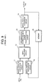
- One of conventional two-dimensional inverse discrete cosine transformation circuits of this kind is disclosed, for example, in the literature "A Single-Chip MPEG1 Audio/Video Decoder" (Y. Katayama, et. al). Structure of the conventional two-dimensional inverse discrete cosine transformation circuit disclosed in the literature is shown in Fig. 9.
- the conventional two-dimensional inverse discrete cosine transformation circuit includes serial-parallel conversion circuits 11 and 16 for conducting 1:8 serial-parallel conversion with respect to input data and outputting converted data, an input switching circuit 12 for receiving input of the outputs of the serial-parallel conversion circuits 11 and 16 and selectively outputting either of them, a one-dimensional inverse discrete cosine transformation circuit 13 for receiving input of the output of the input switching circuit 12 to conduct one-dimensional inverse discrete cosine transformation, a serial-parallel conversion circuit 14 for receiving input of the output of the one-dimensional inverse discrete cosine transformation circuit 13 to conduct 2:1 serial-parallel conversion, and a memory 15 for receiving input of the output of the serial-parallel conversion circuit 14 and temporarily storing and then outputting the same to the serial-parallel conversion circuit 16.
- the input switching circuit 12 switches input to the one-dimensional inverse discrete cosine transformation circuit 13 from the serial-parallel conversion circuit 11 to the serial-parallel conversion circuit 16.
- the data written at the memory 15 is recursively input to the one-dimensional inverse discrete cosine transformation circuit 13 through the serial-parallel conversion circuit 16.
- the serial-parallel conversion circuit 16 sequentially reads data on the basis of a column of the addresses of the memory 15 to conduct 1:8 serial-parallel conversion.
- the data again subjected to serial-parallel conversion is applied to the one-dimensional inverse discrete cosine transformation circuit 13 via the input switching circuit 12, so that the one-dimensional inverse discrete cosine transformation circuit 13 conducts one-dimensional inverse discrete cosine transformation in the same manner as in the first transformation.
- the output data thus subjected to the one-dimensional inverse discrete cosine transformation twice is output through the serial-parallel conversion circuit 14 as output data of the two-dimensional inverse discrete cosine transformation circuit.
- Two-dimensional inverse discrete cosine transformation here is transformation expressed by the following equation (2).
- Fig. 10 when data input starts at T0, every time input of eight data is completed, the data is applied to the one-dimensional inverse discrete cosine transformation circuit 13 (Fig. 10, L0, L1, ). At this time, since the one-dimensional inverse discrete cosine transformation circuit 13 is capable of processing two data at one clock, input to the one-dimensional inverse discrete cosine transformation circuit 13 only needs to be conducted at four clocks. At the remaining four clocks before eight subsequent input data is accumulated, the one-dimensional inverse discrete cosine transformation circuit 13 is at an input waiting state (Fig. 10, 100). Every time data is applied to the one-dimensional inverse discrete cosine transformation circuit 13 at timing L0, L1, ..., data (Fig. 10, L'0, L'1, ...) is calculated whose first one-dimensional inverse discrete cosine transformation is completed after a period of an internal processing time (Fig. 10, 200) of the one-dimensional inverse discrete cosine transformation circuit 13.
- the conventional inverse discrete cosine transformation circuits need to conduct first one-dimensional inverse discrete cosine transformation with respect to all the 64 data and then conduct second one-dimensional inverse discrete cosine transformation after switching input. During the execution of the second one-dimensional inverse discrete cosine transformation, no new data input is acceptable. As a result, much time is required for the processing of data of one block, that is, 64 data.
- An object of the present invention is to provide a two-dimensional inverse discrete cosine transformation circuit of an MPEG2 video decoder which enables reduction of two-dimensional inverse discrete cosine transformation processing time without changing circuit scale.
- a two-dimensional inverse discrete cosine transformation circuit of an MPEG2 video decoder which conducts two-dimensional inverse discrete cosine transformation by subjecting block data composed of a plurality of data to one-dimensional inverse discrete cosine transformation twice, comprises
- the input switching control means may transmit an input switching signal instructing on the switching of the input switching means at every predetermined times of operation clocks, the input switching means may switch output data on condition of the reception of the input switching signal, and the data allocation means may switch an output destination of the output data of the third serial-parallel conversion means according to the setting taking a delay by an internal processing time of the one-dimensional inverse discrete cosine transformation means into consideration on condition of the reception of the input switching signal.
- the input switching control means may transmit an input switching signal instructing on the switching of the input switching means at every one operation clock, the input switching means may switch output data at every one operation clock on condition of the reception of the input switching signal, and the data allocation means may switch an output destination of the output data of the third serial-parallel conversion means at every one operation clock according to the setting taking a delay by an internal processing time of the one-dimensional inverse discrete cosine transformation means into consideration on condition of the reception of the input switching signal.
- the storage means has an address space forming a square matrix, when data of one block applied from the data allocation means is stored along a row of the address space in order, reads the data along a column of the address space and sequentially stores data of a subsequent block applied next from the data allocation means along the column of the address space from which the data has been read, and when data of one block applied from the data allocation means is stored along a column of the address space in order, reads the data along a row of the address space and sequentially stores data of a subsequent block applied next from the data allocation means along the row of the address space from which the data has been read.
- the input switching control means transmits an input switching signal instructing on the switching of the input switching means at every predetermined times of operation clocks, the input switching means switches output data on condition of the reception of the input switching signal, the data allocation means switches an output destination of the output data of the third serial-parallel conversion means according to the setting taking a delay by an internal processing time of the one-dimensional inverse discrete cosine transformation means into consideration on condition of the reception of the input switching signal, and the storage means has an address space forming a square matrix, when data of one block applied from the data allocation means is stored along a row of the address space in order, reads the data along a column of the address space and sequentially stores data of a subsequent block applied next from the data allocation means along the column of the address space from which the data has been read, and when data of one block applied from the data allocation means is stored along a column of the address space in order, reads the data along a row of the address space and sequentially stores data of a subsequent block applied next from the data allocation means along the
- the input switching control means transmits an input switching signal instructing on the switching of the input switching means at every one operation clock
- the input switching means switches output data at every one operation clock on condition of the reception of the input switching signal
- the data allocation means switches an output destination of the output data of the third serial-parallel conversion means at every one operation clock according to the setting taking a delay by an internal processing time of the one-dimensional inverse discrete cosine transformation means into consideration on condition of the reception of the input switching signal
- the storage means has an address space forming a square matrix, when data of one block applied from the data allocation means is stored along a row of the address space in order, reads the data along a column of the address space and sequentially stores data of a subsequent block applied next from the data allocation means along the column of the address space from which the data has been read, and when data of one block applied from the data allocation means is stored along a column of the address space in order, reads the data along a row of the address space and sequentially stores data of a subsequent block applied next from
- the storage means has an address space forming a square matrix of eight rows by eight columns, when data of one block applied from the data allocation means is stored along a row of the address space in order, reads the data along a column of the address space and sequentially stores data of a subsequent block applied next from the data allocation means along the column of the address space from which the data has been read, and when data of one block applied from the data allocation means is stored along a column of the address space in order, reads the data along a row of the address space and sequentially stores data of a subsequent block applied next from the data allocation means along the row of the address space from which the data has been read.
- the input switching control means transmits an input switching signal instructing on the switching of the input switching means at every predetermined times of operation clocks, the input switching means switches output data on condition of the reception of the input switching signal, the data allocation means switches an output destination of the output data of the third serial-parallel conversion means according to the setting taking a delay by an internal processing time of the one-dimensional inverse discrete cosine transformation means into consideration on condition of the reception of the input switching signal, and
- the input switching control means transmits an input switching signal instructing on the switching of the input switching means at every one operation clock, the input switching means switches output data at every one operation clock on condition of the reception of the input switching signal, the data allocation means switches an output destination of the output data of the third serial-parallel conversion means at every one operation clock according to the setting taking a delay by an internal processing time of the one-dimensional inverse discrete cosine transformation means into consideration on condition of the reception of the input switching signal, and
- Fig. 1 is a block diagram showing structure of a two-dimensional inverse discrete cosine transformation circuit according to one embodiment of the present invention.
- the two-dimensional inverse discrete cosine transformation circuit of the present embodiment includes serial-parallel conversion circuits 11 and 16 for conducting 1:8 serial-parallel conversion with respect to input data and outputting converted data, an input switching circuit 12 for receiving input of outputs of the serial-parallel conversion circuits 11 and 16 and selectively outputting either of the outputs, a one-dimensional inverse discrete cosine transformation circuit 13 for receiving input of the output of the input switching circuit 12 to conduct one-dimensional inverse discrete cosine transformation, a serial-parallel conversion circuit 14 for receiving input of the output of the one-dimensional inverse discrete cosine transformation circuit 13 to conduct 2:1 serial-parallel conversion, a memory 15 for receiving input of the output of the serial-parallel conversion circuit 14 and temporarily storing and then outputting the same to the serial-parallel conversion circuit 16, an input switching control circuit 17 for controlling operation of the input switching circuit 12 according to an operation clock, a data allocation circuit 18 for controlling an output destination of the output of the serial-parallel conversion
- the first serial-parallel conversion circuit 11 conducts 1:8 parallel conversion with respect to input data applied through an input pin and sends eight each of converted data to the input switching circuit 12.
- the second serial-parallel conversion circuit 16 reads data from the memory 15 and conducts 1:8 parallel conversion with respect to the read data to send eight each of converted data to the input switching circuit 12.
- the input switching circuit 12 selects either of eight data from the first serial-parallel conversion circuit 11 or eight data from the second serial-parallel conversion circuit 16 in response to an input switching signal from the input switching control circuit 17 and inputs the selected data to the one-dimensional inverse discrete cosine transformation circuit 13. It is assumed for example that when the input switching signal is at a state of "0", the circuit 12 selects eight data from the first serial-parallel conversion circuit 11 and when the signal is at a state of "1", the circuit selects eight data from the second serial-parallel conversion circuit 16.
- the one-dimensional inverse discrete cosine transformation circuit 13 conducts the one-dimensional inverse discrete cosine transformation expressed by the above equation (1) with respect to output data from the serial-parallel conversion circuit 11 or 16 applied through the input switching circuit 12.
- An example of structure of the one-dimensional inverse discrete cosine transformation circuit 13 is shown in Fig. 2.
- P0, P1, P2, P3, P4, P5 and P6 represent multipliers with cos7 ⁇ /16, cos3 ⁇ /8, cos5 ⁇ /16, cos ⁇ /4, cos3 ⁇ /16, cos ⁇ /8 and cos ⁇ /16 as coefficients, respectively.
- EX represents a circuit which determines a sign + or - for an output value of the multiplier according to the operation expression.
- Data F(0), F(1), ..., F(7) applied to the one-dimensional inverse discrete cosine transformation circuit 13 is converted into f(0), f(1), ..., f(7), respectively, which is output in four clocks according to butterfly operation, that is, two each data is output at one clock, like "f(0), f(7)", “f(1), f(6)", “f(2), f(5)” and "f(3), f(4)".
- the third serial-parallel conversion circuit 14 conducts 2:1 serial-parallel conversion with respect to output data of the one-dimensional inverse discrete cosine transformation circuit 13. More specifically, the circuit 14 converts two each parallel data which is output at one clock into serial data and outputs the converted data.
- the data allocation circuit 18 controls an output destination of output data of the serial-parallel conversion circuit 14 by switching based on the input switching signal output from the input switching control circuit 17. More specifically, output data which has been read from the memory 15, applied to the one-dimensional inverse discrete cosine transformation circuit 13 through the second serial-parallel conventional circuit 16 and subjected to one-dimensional inverse discrete cosine transformation is output to the output pin. Output data which has been applied through the input pin, applied to the one-dimensional inverse discrete cosine transformation circuit 13 through the first serial-parallel conversion circuit 11 and subjected to one-dimensional inverse discrete cosine transformation is output to the memory 15. Output destination switching timing is set based on an internal processing time of the one-dimensional inverse discrete cosine transformation circuit 13 and is determined based on the input switching signal of the input switching control circuit 17.
- the memory 15 generates an address in response to a memory address switching signal from the memory address control unit 19 to conduct read and write of data.
- An example of structure of the memory 15 is shown in Fig. 3.
- a memory cell 31 is a dual port RAM.
- a counter 34 is a 6-bit counter which is incremented when a read enable signal is at the state of 1.
- a counter 35 is a 6-bit counter which is incremented when a write enable signal is at the state of 1.
- the counters 34 and 35 are both reset by an input start signal.
- a read address decoder 32 decodes the value of the counter 34 in response to the memory address switching signal from the memory address control unit 19 and generates a read address to read data.
- a write address decoder 33 decodes the value of the counter 35 in response to the memory address switching signal from the memory address control unit 19 and generates a write address to write data.
- the value of the counter 34 will be larger than that of the counter 35 at any time. Therefore, in the memory cell 31, no new data will be overwritten at an address from which data is yet to be read.
- the input switching control circuit 17 which is composed only of a binary counter, has an input switching signal as its output signal reset to the state of "0" when input from the input pin starts and incremented at every clock.
- the memory address control unit 19 which is composed only of a binary counter, has a memory address switching signal as its output signal set to the state of "1" as an initial value and incremented when input from the input pin starts.
- a memory address switching signal output from the memory address control unit 19 is at the state of "1" before T0.
- an internal processing time of the one-dimensional inverse discrete cosine transformation circuit 13 is assumed to be five clocks.
- the data allocation circuit 18 is assumed to send data to the memory 15 when the input switching signal output from the input switching control circuit 17 is at the state of "1" and to output data to the output pin when the signal is at the state of "0".
- Stored in the memory 15 is one block of 64 data which has been subjected to first one-dimensional inverse discrete cosine transformation. This data is referred to as data of a previous block subjected to one-dimensional inverse discrete cosine transformation.
- the input switching signal of the input switching control circuit 17 is reset to the state of "0", so that the state of the memory address switching signal of the memory address control unit 19 changes from the state of "1" to "0".
- the state of the input switching signal is switched between the state of "1" and "0" at every one clock.
- the serial-parallel conversion circuit 16 reads data of a previous block subjected to one-dimensional inverse discrete cosine transformation which is stored in the memory 15 one by one at every one clock. At this time, since the memory address switching signal is at the state of "0", data is read in a row direction of the addresses of the memory 15.
- the one-dimensional inverse discrete cosine transformation circuit 13 is allowed to continuously receive input of data at any time without entering an input waiting state.
- the one-dimensional inverse discrete cosine transformation circuit 13 thus alternately outputs, at every one clock, two each of data obtained by subjecting input data to the first one-dimensional inverse discrete cosine transformation and two each of data obtained by subjecting data of a previous block which has been read from the memory 15 and then subjected to one-dimensional inverse discrete cosine transformation to the second one-dimensional inverse discrete cosine transformation. Then, the data allocation circuit 18 alternately switches and outputs the output data to the memory 15 and the output pin at every one clock.
- one-dimensional inverse discrete cosine transformation is completed with respect to all of the 64 data applied through the input pin and the 64 data of the previous block subjected to one-dimensional inverse discrete cosine transformation.
- the data applied through the input pin will have been written at the memory 15 as data of one block whose one-dimensional inverse discrete cosine transformation has been finished, and the data of the previous block whose one-dimensional inverse discrete cosine transformation has been finished will have been externally output.
- the data in question stored in the memory 15 is read out to the serial-parallel conversion circuit 16 as data of a previous block whose one-dimensional inverse discrete cosine transformation has been finished.
- the memory address switching signal changes from the state of "0" to the state of "1”, so that data reading from the memory 15 is conducted in a column direction.
- the read block data is subjected to the second one-dimensional inverse discrete cosine transformation in a column direction.
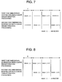
- a time required for conducting two-dimensional inverse discrete cosine transformation with respect to block data of k blocks will be represented as (k+1)S as shown in Fig. 8.
- a time required for processing block data of one block in a conventional two-dimensional inverse discrete cosine transformation circuit denoted as 2T
- a time required for processing block data of k blocks will be represented as 2kT as shown in Fig. 7.
- the present invention has been described with respect to the preferred embodiment in the foregoing, the present invention is not limited to the above-described embodiment.
- the internal processing time of the one-dimensional inverse discrete cosine transformation circuit is five clocks and that in a case where the data allocation circuit switches an output destination of output data of the one-dimensional inverse discrete cosine transformation circuit, the output data is sent to the memory when the input switching signal of the input switching control circuit is at the state of "1" and to the output pin when the signal is at the state of "0".
- the internal processing time of the one-dimensional inverse discrete cosine transformation circuit may have other value than five clocks.
- the output destination is switched by the data allocation circuit to the output pin when the input switching signal is at the state of "1" and is switched to the memory when the signal is at the state of "0".
- the output data is sent to the memory when the input switching signal is at the state of "1” and sent to the output pin when the signal is at the state of "0".
- new block data applied from the input pin and previous block data subjected to one-dimensional inverse discrete cosine transformation processing once is applied to the one-dimensional inverse discrete cosine transformation circuit alternately at every one clock
- the data to be applied may be switched not at every one clock but at every two clocks or four clocks.
- switching timing of the input switching circuit and the data allocation circuit should be appropriately modified according to the setting of the one-dimensional inverse discrete cosine transformation circuit.
- two-dimensional discrete cosine transformation which is equivalent to inverse transformation of two-dimensional inverse discrete cosine transformation.
- two-dimensional discrete cosine transformation can be implemented by replacing the one-dimensional inverse discrete cosine transformation circuit in the structure of the present invention with a one-dimensional discrete cosine transformation circuit and operating and controlling the latter circuit in the same manner as in the present invention.
- the two-dimensional inverse discrete cosine transformation circuit of an MPEG2 video decoder is allowed to receive input of data efficiently without a waiting time when data is applied to the one-dimensional inverse discrete cosine transformation circuit, whereby reduction of a processing time can be achieved which is required for conducting two-dimensional inverse discrete cosine transformation processing with respect to a plurality of block data. With the number of block data to be processed large enough, the processing time can be substantially reduced by half.
- the present invention realizes the above-described effects with ease because it obtains the above-described effects by its unique circuit control without changing circuit scale.
Landscapes
- Physics & Mathematics (AREA)
- General Physics & Mathematics (AREA)
- Engineering & Computer Science (AREA)
- Mathematical Physics (AREA)
- Theoretical Computer Science (AREA)
- Data Mining & Analysis (AREA)
- Mathematical Optimization (AREA)
- Pure & Applied Mathematics (AREA)
- Mathematical Analysis (AREA)
- Discrete Mathematics (AREA)
- Computational Mathematics (AREA)
- Software Systems (AREA)
- Databases & Information Systems (AREA)
- General Engineering & Computer Science (AREA)
- Algebra (AREA)
- Multimedia (AREA)
- Compression Or Coding Systems Of Tv Signals (AREA)
- Compression Of Band Width Or Redundancy In Fax (AREA)
- Complex Calculations (AREA)
- Compression, Expansion, Code Conversion, And Decoders (AREA)
Abstract
Description

Claims (9)
- A two-dimensional inverse discrete cosine transformation circuit of an MPEG2 video decoder which conducts two-dimensional inverse discrete cosine transformation by subjecting block data composed of a plurality of data to one-dimensional inverse discrete cosine transformation twice, comprising:first serial-parallel conversion means (11) for parallel-converting externally applied new input data and outputting the converted data;storage means (15) for storing data of a previous block already subjected to first one-dimensional inverse discrete cosine transformation;second serial-parallel conversion means (16) for obtaining said data of a previous block from said storage means (15), parallel-converting said data and outputting said converted data;input switching means (12) for receiving input of data output from said first serial-parallel conversion means (11) and data output from said second serial-parallel conversion means (16) and selectively switching and outputting one of them;input switching control means (17) for controlling operation of said input switching means (12);one-dimensional inverse discrete cosine transformation means (13) for conducting one-dimensional inverse discrete cosine transformation with respect to data applied through said input switching means (12);third serial-parallel conversion means (14) for serial-converting and outputting output data of said one-dimensional inverse discrete cosine transformation means (13); anddata allocation means (18) for controlling an output destination of output data of said third serial-parallel conversion means (14) by switching under the control of said input switching means (12) and said input switching control means (17) to send data subjected to first one-dimensional inverse discrete cosine transformation to said storage means (15) and externally output data subjected to second one-dimensional inverse discrete cosine transformation;said input switching control means (17) controlling said input switching means (12) to alternately and continuously output the data output from said first serial-parallel conversion means (11) and the data output from said second serial-parallel conversion means (16) at every predetermined times of operation clocks, andsaid data allocation means (18) switching an output destination of the output data of said third serial-parallel conversion means (14) at timing delayed by an internal processing time of said one-dimensional inverse discrete cosine transformation means (13) from the timing of switching of said input switching means (12) by said input switching control means (17).
- The second-dimensional inverse discrete cosine transformation circuit as set forth in claim 1, whereinsaid input switching control means (17) transmits an input switching signal instructing on the switching of said input switching means (12) at every predetermined times of operation clocks,said input switching means (12) switches output data on condition of the reception of said input switching signal, andsaid data allocation means (18) switches an output destination of the output data of said third serial-parallel conversion means (14) according to the setting taking a delay by an internal processing time of said one-dimensional inverse discrete cosine transformation means (13) into consideration on condition of the reception of said input switching signal.
- The two-dimensional inverse discrete cosine transformation circuit as set forth in claim 1, whereinsaid input switching control means (17) transmits an input switching signal instructing on the switching of said input switching means (12) at every one operation clock,said input switching means (12) switches output data at every one operation clock on condition of the reception of said input switching signal, andsaid data allocation means (18) switches an output destination of the output data of said third serial-parallel conversion means (14) at every one operation clock according to the setting taking a delay by an internal processing time of said one-dimensional inverse discrete cosine transformation means (13) into consideration on condition of the reception of said input switching signal.
- The two-dimensional inverse discrete cosine transformation circuit as set forth in claim 1, whereinsaid storage means (15)has an address space forming a square matrix,when data of one block applied from said data allocation means (18) is stored along a row of said address space in order, reads the data along a column of said address space and sequentially stores data of a subsequent block applied next from said data allocation means (18) along said column of the address space from which said data has been read, andwhen data of one block applied from said data allocation means (18) is stored along a column of said address space in order, reads the data along a row of said address space and sequentially stores data of a subsequent block applied next from said data allocation means (18) along said row of the address space from which said data has been read.
- The second-dimensional inverse discrete cosine transformation circuit as set forth in claim 1, whereinsaid input switching control means (17) transmits an input switching signal instructing on the switching of said input switching means (12) at every predetermined times of operation clocks,said input switching means (12) switches output data on condition of the reception of said input switching signal,said data allocation means (18) switches an output destination of the output data of said third serial-parallel conversion means (14) according to the setting taking a delay by an internal processing time of said one-dimensional inverse discrete cosine transformation means (13) into consideration on condition of the reception of said input switching signal, andsaid storage means (15)has an address space forming a square matrix,when data of one block applied from said data allocation means (18) is stored along a row of said address space in order, reads the data along a column of said address space and sequentially stores data of a subsequent block applied next from said data allocation means (18) along said column of the address space from which said data has been read, andwhen data of one block applied from said data allocation means (18) is stored along a column of said address space in order, reads the data along a row of said address space and sequentially stores data of a subsequent block applied next from said data allocation means (18) along said row of the address space from which said data has been read.
- The two-dimensional inverse discrete cosine transformation circuit as set forth in claim 1, whereinsaid input switching control means (17) transmits an input switching signal instructing on the switching of said input switching means (12) at every one operation clock,said input switching means (12) switches output data at every one operation clock on condition of the reception of said input switching signal,said data allocation means (18) switches an output destination of the output data of said third serial-parallel conversion means (14) at every one operation clock according to the setting taking a delay by an internal processing time of said one-dimensional inverse discrete cosine transformation means (13) into consideration on condition of the reception of said input switching signal, andsaid storage means (15)has an address space forming a square matrix,when data of one block applied from said data allocation means (18) is stored along a row of said address space in order, reads the data along a column of said address space and sequentially stores data of a subsequent block applied next from said data allocation means (18) along said column of the address space from which said data has been read, andwhen data of one block applied from said data allocation means (18) is stored along a column of said address space in order, reads the data along a row of said address space and sequentially stores data of a subsequent block applied next from said data allocation means (18) along said row of the address space from which said data has been read.
- The two-dimensional inverse discrete cosine transformation circuit as set forth in claim 1, whereinsaid storage means (15)has an address space forming a square matrix of eight rows by eight columns,when data of one block applied from said data allocation means (18) is stored along a row of said address space in order, reads the data along a column of said address space and sequentially stores data of a subsequent block applied next from said data allocation means (18) along said column of the address space from which said data has been read, andwhen data of one block applied from said data allocation means (18) is stored along a column of said address space in order, reads the data along a row of said address space and sequentially stores data of a subsequent block applied next from said data allocation means (18) along said row of the address space from which said data has been read.
- The second-dimensional inverse discrete cosine transformation circuit as set forth in claim 1, whereinsaid input switching control means (17) transmits an input switching signal instructing on the switching of said input switching means (12) at every predetermined times of operation clocks,said input switching means (12) switches output data on condition of the reception of said input switching signal,said data allocation means (18) switches an output destination of the output data of said third serial-parallel conversion means (14) according to the setting taking a delay by an internal processing time of said one-dimensional inverse discrete cosine transformation means (13) into consideration on condition of the reception of said input switching signal, andsaid storage means (15)has an address space forming a square matrix of eight rows by eight columns,when data of one block applied from said data allocation means (18) is stored along a row of said address space in order, reads the data along a column of said address space and sequentially stores data of a subsequent block applied next from said data allocation means (18) along said column of the address space from which said data has been read, andwhen data of one block applied from said data allocation means (18) is stored along a column of said address space in order, reads the data along a row of said address space and sequentially stores data of a subsequent block applied next from said data allocation means (18) along said row of the address space from which said data has been read.
- The two-dimensional inverse discrete cosine transformation circuit as set forth in claim 1, whereinsaid input switching control means (17) transmits an input switching signal instructing on the switching of said input switching means (12) at every one operation clock,said input switching means (12) switches output data at every one operation clock on condition of the reception of said input switching signal,said data allocation means (18) switches an output destination of the output data of said third serial-parallel conversion means (14) at every one operation clock according to the setting taking a delay by an internal processing time of said one-dimensional inverse discrete cosine transformation means (13) into consideration on condition of the reception of said input switching signal, andsaid storage means (15)has an address space forming a square matrix of eight rows by eight columns,when data of one block applied from said data allocation means (18) is stored along a row of said address space in order, reads the data along a column of said address space and sequentially stores data of a subsequent block applied next from said data allocation means (18) along said column of the address space from which said data has been read, andwhen data of one block applied from said data allocation means (18) is stored along a column of said address space in order, reads the data along a row of said address space and sequentially stores data of a subsequent block applied next from said data allocation means (18) along said row of the address space from which said data has been read.
Applications Claiming Priority (3)
| Application Number | Priority Date | Filing Date | Title |
|---|---|---|---|
| JP27163196A JP3092526B2 (en) | 1996-09-20 | 1996-09-20 | 2D inverse discrete cosine transform circuit |
| JP27163196 | 1996-09-20 | ||
| JP271631/96 | 1996-09-20 |
Publications (2)
| Publication Number | Publication Date |
|---|---|
| EP0831404A2 true EP0831404A2 (en) | 1998-03-25 |
| EP0831404A3 EP0831404A3 (en) | 1999-10-20 |
Family
ID=17502768
Family Applications (1)
| Application Number | Title | Priority Date | Filing Date |
|---|---|---|---|
| EP19970116103 Withdrawn EP0831404A3 (en) | 1996-09-20 | 1997-09-16 | Two-dimensional inverse discrete cosine transform circuit |
Country Status (3)
| Country | Link |
|---|---|
| US (1) | US5978508A (en) |
| EP (1) | EP0831404A3 (en) |
| JP (1) | JP3092526B2 (en) |
Families Citing this family (6)
| Publication number | Priority date | Publication date | Assignee | Title |
|---|---|---|---|---|
| US6175594B1 (en) * | 1998-05-22 | 2001-01-16 | Ati Technologies, Inc. | Method and apparatus for decoding compressed video |
| WO2001035267A1 (en) * | 1999-11-12 | 2001-05-17 | Bops, Incorporated | Methods and apparatus for efficient cosine transform implementations |
| US6754687B1 (en) | 1999-11-12 | 2004-06-22 | Pts Corporation | Methods and apparatus for efficient cosine transform implementations |
| JP2006260411A (en) * | 2005-03-18 | 2006-09-28 | Japan Radio Co Ltd | Signal processor, and communication equipment using the same |
| JP2006319837A (en) * | 2005-05-16 | 2006-11-24 | Rohm Co Ltd | Image processing apparatus |
| US7750974B2 (en) * | 2005-11-10 | 2010-07-06 | Broadcom Corporation | System and method for static region detection in video processing |
Citations (6)
| Publication number | Priority date | Publication date | Assignee | Title |
|---|---|---|---|---|
| EP0424119A2 (en) * | 1989-10-19 | 1991-04-24 | Zoran Corporation | Recycling DCT/IDCT integrated circuit apparatus using a single multiplier/accumulator and a single random access memory |
| US5181183A (en) * | 1990-01-17 | 1993-01-19 | Nec Corporation | Discrete cosine transform circuit suitable for integrated circuit implementation |
| EP0566184A2 (en) * | 1992-04-13 | 1993-10-20 | Koninklijke Philips Electronics N.V. | Picture transformer and television system with a transmitter and a receiver comprising a picture transformer |
| JPH07234863A (en) * | 1993-12-27 | 1995-09-05 | Matsushita Electric Ind Co Ltd | Two-dimensional orthogonal transformation device |
| DE19520962C1 (en) * | 1995-03-18 | 1996-06-13 | United Microelectronics Corp | Two-dimensional discrete real-time cosine transformation circuit or cosine reverse transformation circuit |
| US5550765A (en) * | 1994-05-13 | 1996-08-27 | Lucent Technologies Inc. | Method and apparatus for transforming a multi-dimensional matrix of coefficents representative of a signal |
Family Cites Families (7)
| Publication number | Priority date | Publication date | Assignee | Title |
|---|---|---|---|---|
| US5054103A (en) * | 1987-09-24 | 1991-10-01 | Matsushita Electric Works, Ltd. | Picture encoding system |
| JPH01201773A (en) * | 1988-02-05 | 1989-08-14 | Matsushita Electric Ind Co Ltd | Digital signal processor |
| JPH04277932A (en) * | 1991-03-06 | 1992-10-02 | Nec Corp | Image data compressing device |
| JP2622049B2 (en) * | 1991-05-24 | 1997-06-18 | 松下電器産業株式会社 | Cable broadcasting system |
| JP3546437B2 (en) * | 1993-03-31 | 2004-07-28 | ソニー株式会社 | Adaptive video signal processing unit |
| JP4035789B2 (en) * | 1994-10-13 | 2008-01-23 | 富士通株式会社 | Inverse discrete cosine transform device |
| JPH08235159A (en) * | 1994-12-06 | 1996-09-13 | Matsushita Electric Ind Co Ltd | Inverse cosine transformation device |
-
1996
- 1996-09-20 JP JP27163196A patent/JP3092526B2/en not_active Expired - Fee Related
-
1997
- 1997-09-16 EP EP19970116103 patent/EP0831404A3/en not_active Withdrawn
- 1997-09-18 US US08/933,079 patent/US5978508A/en not_active Expired - Fee Related
Patent Citations (6)
| Publication number | Priority date | Publication date | Assignee | Title |
|---|---|---|---|---|
| EP0424119A2 (en) * | 1989-10-19 | 1991-04-24 | Zoran Corporation | Recycling DCT/IDCT integrated circuit apparatus using a single multiplier/accumulator and a single random access memory |
| US5181183A (en) * | 1990-01-17 | 1993-01-19 | Nec Corporation | Discrete cosine transform circuit suitable for integrated circuit implementation |
| EP0566184A2 (en) * | 1992-04-13 | 1993-10-20 | Koninklijke Philips Electronics N.V. | Picture transformer and television system with a transmitter and a receiver comprising a picture transformer |
| JPH07234863A (en) * | 1993-12-27 | 1995-09-05 | Matsushita Electric Ind Co Ltd | Two-dimensional orthogonal transformation device |
| US5550765A (en) * | 1994-05-13 | 1996-08-27 | Lucent Technologies Inc. | Method and apparatus for transforming a multi-dimensional matrix of coefficents representative of a signal |
| DE19520962C1 (en) * | 1995-03-18 | 1996-06-13 | United Microelectronics Corp | Two-dimensional discrete real-time cosine transformation circuit or cosine reverse transformation circuit |
Non-Patent Citations (4)
| Title |
|---|
| MADISETTI A ET AL: "A 100 MHZ 2-D 8 X 8 DCT/IDCT PROCESSOR FOR HDTV APPLICATIONS" IEEE TRANSACTIONS ON CIRCUITS AND SYSTEMS FOR VIDEO TECHNOLOGY, vol. 5, no. 2, 1 April 1995 (1995-04-01), pages 158-165, XP000509201 ISSN: 1051-8215 * |
| PATENT ABSTRACTS OF JAPAN vol. 096, no. 001, 31 January 1996 (1996-01-31) & JP 07 234863 A (MATSUSHITA ELECTRIC IND CO LTD), 5 September 1995 (1995-09-05) * |
| S. WOLTER, D. BIRRECK, R. LAUR: "Classification for 2D-DCTs and a New Architecture with Distributed Arithmetic" 1991 IEEE INTERNATIONAL SYMPOSIUM ON CIRCUITS AND SYSTEMS, 11 - 14 June 1991, pages 2204-2207, XP002112505 Singapore * |
| SMITH S G ET AL: "GENERIC ASIC ARCHITECTURE AND SYNTHESIS SCHEME FOR DSP" SPECTRAL ESTIMATION, VLSI, UNDERWATER SIGNAL PROCESSING, GLASGOW, MAY 23 - 26, 1989, vol. 4, no. CONF. 14, 23 May 1989 (1989-05-23), pages 2413-2416, XP000090102 INSTITUTE OF ELECTRICAL AND ELECTRONICS ENGINEERS * |
Also Published As
| Publication number | Publication date |
|---|---|
| EP0831404A3 (en) | 1999-10-20 |
| JP3092526B2 (en) | 2000-09-25 |
| JPH1097519A (en) | 1998-04-14 |
| US5978508A (en) | 1999-11-02 |
Similar Documents
| Publication | Publication Date | Title |
|---|---|---|
| US5329318A (en) | Method for optimizing image motion estimation | |
| US5386233A (en) | Method for efficient memory use | |
| US5684534A (en) | Task-splitting dual-processor system for motion estimation processing | |
| EP0169709B1 (en) | Real time processor for video signals | |
| US5446839A (en) | Method for controlling dataflow between a plurality of circular buffers | |
| US5210705A (en) | Digital filtering with single-instruction, multiple-data processor | |
| JP2750438B2 (en) | Two-dimensional pixel interpolator and method for generating two-dimensional interpolated pixel values | |
| US5469208A (en) | Dequantization using decrements and multiply | |
| US5659776A (en) | Method and apparatus for inputting data to a single instruction, multiple data processor used in a television receiving system | |
| US5610849A (en) | Real time two-dimensional discrete cosine transform/inverse discrete cosine transform circuit | |
| WO1995032578A2 (en) | Mpeg decoder | |
| US6223193B1 (en) | Macroblock variance estimator for MPEG-2 video encoder | |
| EP0592351A2 (en) | Image decoder | |
| US5528528A (en) | Method, apparatus, and system for transforming signals | |
| US5592399A (en) | Pipelined video encoder architecture | |
| EP0831404A2 (en) | Two-dimensional inverse discrete cosine transform circuit | |
| US5426462A (en) | Apparatus for encoding signals using a configurable transform circuit | |
| US7292730B1 (en) | Two-dimensional inverse discrete cosine transforming | |
| JP2960328B2 (en) | Apparatus for providing operands to "n + 1" operators located in a systolic architecture | |
| JP2851804B2 (en) | 2D orthogonal transform device | |
| JP3352346B2 (en) | Image signal processing device | |
| JPH10341438A (en) | Image processor | |
| JPH06274607A (en) | Parallel signal processor | |
| KR100275269B1 (en) | Inverse-quantizer | |
| KR960006585A (en) | Scan type conversion circuit |
Legal Events
| Date | Code | Title | Description |
|---|---|---|---|
| PUAI | Public reference made under article 153(3) epc to a published international application that has entered the european phase |
Free format text: ORIGINAL CODE: 0009012 |
|
| AK | Designated contracting states |
Kind code of ref document: A2 Designated state(s): DE FR NL |
|
| AX | Request for extension of the european patent |
Free format text: AL;LT;LV;RO;SI |
|
| PUAL | Search report despatched |
Free format text: ORIGINAL CODE: 0009013 |
|
| AK | Designated contracting states |
Kind code of ref document: A3 Designated state(s): AT BE CH DE DK ES FI FR GB GR IE IT LI LU MC NL PT SE |
|
| AX | Request for extension of the european patent |
Free format text: AL;LT;LV;RO;SI |
|
| 17P | Request for examination filed |
Effective date: 20000105 |
|
| AKX | Designation fees paid |
Free format text: DE FR NL |
|
| RAP1 | Party data changed (applicant data changed or rights of an application transferred) |
Owner name: NEC ELECTRONICS CORPORATION |
|
| STAA | Information on the status of an ep patent application or granted ep patent |
Free format text: STATUS: THE APPLICATION HAS BEEN WITHDRAWN |
|
| 18W | Application withdrawn |
Effective date: 20080305 |