EP0821844B1 - Procede de traitement d'ondes pwm et dispositifs appliquant ce procede - Google Patents
Procede de traitement d'ondes pwm et dispositifs appliquant ce procede Download PDFInfo
- Publication number
- EP0821844B1 EP0821844B1 EP96908936A EP96908936A EP0821844B1 EP 0821844 B1 EP0821844 B1 EP 0821844B1 EP 96908936 A EP96908936 A EP 96908936A EP 96908936 A EP96908936 A EP 96908936A EP 0821844 B1 EP0821844 B1 EP 0821844B1
- Authority
- EP
- European Patent Office
- Prior art keywords
- inverter
- current
- rectifier
- voltage
- corrected
- Prior art date
- Legal status (The legal status is an assumption and is not a legal conclusion. Google has not performed a legal analysis and makes no representation as to the accuracy of the status listed.)
- Expired - Lifetime
Links
Images


Classifications
-
- H—ELECTRICITY
- H02—GENERATION; CONVERSION OR DISTRIBUTION OF ELECTRIC POWER
- H02M—APPARATUS FOR CONVERSION BETWEEN AC AND AC, BETWEEN AC AND DC, OR BETWEEN DC AND DC, AND FOR USE WITH MAINS OR SIMILAR POWER SUPPLY SYSTEMS; CONVERSION OF DC OR AC INPUT POWER INTO SURGE OUTPUT POWER; CONTROL OR REGULATION THEREOF
- H02M1/00—Details of apparatus for conversion
- H02M1/38—Means for preventing simultaneous conduction of switches
-
- H—ELECTRICITY
- H02—GENERATION; CONVERSION OR DISTRIBUTION OF ELECTRIC POWER
- H02M—APPARATUS FOR CONVERSION BETWEEN AC AND AC, BETWEEN AC AND DC, OR BETWEEN DC AND DC, AND FOR USE WITH MAINS OR SIMILAR POWER SUPPLY SYSTEMS; CONVERSION OF DC OR AC INPUT POWER INTO SURGE OUTPUT POWER; CONTROL OR REGULATION THEREOF
- H02M1/00—Details of apparatus for conversion
- H02M1/12—Arrangements for reducing harmonics from ac input or output
-
- H—ELECTRICITY
- H02—GENERATION; CONVERSION OR DISTRIBUTION OF ELECTRIC POWER
- H02M—APPARATUS FOR CONVERSION BETWEEN AC AND AC, BETWEEN AC AND DC, OR BETWEEN DC AND DC, AND FOR USE WITH MAINS OR SIMILAR POWER SUPPLY SYSTEMS; CONVERSION OF DC OR AC INPUT POWER INTO SURGE OUTPUT POWER; CONTROL OR REGULATION THEREOF
- H02M7/00—Conversion of ac power input into dc power output; Conversion of dc power input into ac power output
- H02M7/42—Conversion of dc power input into ac power output without possibility of reversal
- H02M7/44—Conversion of dc power input into ac power output without possibility of reversal by static converters
- H02M7/48—Conversion of dc power input into ac power output without possibility of reversal by static converters using discharge tubes with control electrode or semiconductor devices with control electrode
- H02M7/53—Conversion of dc power input into ac power output without possibility of reversal by static converters using discharge tubes with control electrode or semiconductor devices with control electrode using devices of a triode or transistor type requiring continuous application of a control signal
- H02M7/537—Conversion of dc power input into ac power output without possibility of reversal by static converters using discharge tubes with control electrode or semiconductor devices with control electrode using devices of a triode or transistor type requiring continuous application of a control signal using semiconductor devices only, e.g. single switched pulse inverters
- H02M7/539—Conversion of dc power input into ac power output without possibility of reversal by static converters using discharge tubes with control electrode or semiconductor devices with control electrode using devices of a triode or transistor type requiring continuous application of a control signal using semiconductor devices only, e.g. single switched pulse inverters with automatic control of output wave form or frequency
- H02M7/5395—Conversion of dc power input into ac power output without possibility of reversal by static converters using discharge tubes with control electrode or semiconductor devices with control electrode using devices of a triode or transistor type requiring continuous application of a control signal using semiconductor devices only, e.g. single switched pulse inverters with automatic control of output wave form or frequency by pulse-width modulation
Definitions
- the present invention relates to a method of processing of PWM waves intended for an inverter or a controlled rectifier, and more particularly in view obtain the reduction of harmonics.
- the present invention also relates to devices for implementing the method according to the present invention.
- the inverters and more particularly the voltage inverters, are intended to supply a voltage alternative from a DC voltage, while the controlled rectifiers are intended to supply voltage continues from an AC voltage.
- inverters can be used for variable speed control of machines synchronous or asynchronous.
- Voltage inverters are good devices known which generally use assemblies of components such as thyristors, GTOs, ... which switch particularly quickly.
- An inverter is controlled by a modulator and a discriminator.
- the role of the modulator is to create a wave setpoint, while the discriminator allows to separate this wave in several waves intended for the command individual switches.
- the simplest inverters are on two levels and consist of two switches (thyristors, GTO, ...) which supply the load alternately.
- This charge being of selfic type, it is necessary that a diode called “freewheeling diode” is placed in parallel on each switch to allow the charging current to circulate when the corresponding switch is open.
- harmonic 6 which is the most troublesome harmonic, because for a motor powered by 1/6 of the frequency used for signaling, there will be risk of interference. For example, a powered motor at 8 1/3 Hz may cause disturbance in the signaling system which uses 50 Hz.
- Another problem is that different switches cannot switch instantly of a zero value (current flowing and corresponding to the closing) at a positive value of the voltage (zero current and corresponding to the opening) and vice versa. This means that for a certain period of time, we simultaneously have a non-zero voltage and non-zero current, and therefore observes a loss of power on each switching.
- a support unit for switching In order to solve this problem, in case the various components cannot withstand such loss of power, it is known to offer a support unit for switching.
- An example of such a cell can be constituted simply by a "snubber" which includes basically a capacity paralleled on each switch. This snubber aims to absorb the losses of power by limiting the voltage, and more particularly by limiting its growth, when switching.
- Another example of a cell often used in combination with the snubber is the cell called "di / dt", which includes essentially a choke in series with the switches.
- GB-2 238 188 describes a converter controlled by a PWM generator and which has a reference signal generator (setpoint) associated with a zero current level detected by a outgoing current to give a signal to the PWM generator.
- a control is provided to avoid a short circuit between the controllable elements used as switches in the PWM converter which generates an alternating voltage variable or alternating current indicative of a variable frequency.
- a selector chooses an output in the period during which the result of detection by the current detector falls in the region of a zero level substantial by selecting a corresponding signal for each switch which actually acts on the output current production, outside signals generated by a PWM signal generator during a period other than that described above, and producing thus the equivalent of a control signal for the switch.
- the current detector is used to determine the polarity of the output and the control ensured the fact that only the switches generating the output of correct polarity can be ordered.
- the present invention aims to propose a method which makes it possible to reduce, until canceling, the effect of the times dead in a controlled inverter or rectifier, and allows therefore reduce the effect of unwanted harmonics.
- the present invention aims in particular to propose a process that can be applied to inverters or controlled rectifiers, with or without switching, whether two-level or multi-level.
- the present invention aims to propose in the case of a three-phase inverter supplying a synchronous or asynchronous motor, a process which allows reduce unwanted harmonics such as harmonics 5 and 7 appearing in the motor currents, and therefore the harmonic 6 appearing on the supply side and engine torque side.
- the present invention relates to a method for processing PWM waves intended to control a voltage inverter or a voltage rectifier, this inverter or rectifier comprising at least a branch with at least one pair of switches connected in series, by which a modulator creates the PWM control wave in the form of a succession of high and low states, the high state being defined by the fact that the switch connected to the most positive voltage is closed while the switch connected to the most negative voltage is open, and the low state being defined by the reverse, characterized in that the PWM control wave is corrected according to the direction of the current leaving or entering the branch so as to obtain two corrected setpoints, the corrected setpoint for the outgoing current having a high state increased by a delay during the transition from the high state to the low state, and the corrected setpoint for the inrush current t having a low state increased by a delay during the transition from the low state to the high state.
- the corrected instructions introduce deadlines which correspond to the dead time created itself by the discriminator.
- delay introduced in the corrected instructions depends not only of the direction of the current, but also of its value.
- the present invention also relates to a device for implementation of the PWM wave treatment method according to the invention and which are intended to control a voltage inverter or a voltage rectifier, the inverter or rectifier comprising at least one branch with at least one pair of switches connected in series, the device comprising a modulator creating the PWM control wave in the form of a succession of high and low states, the state high being defined by the fact that the switch connected to the most positive voltage is closed while the switch connected to the most negative voltage is open, and the low state being defined by the reverse, characterized in that means of correction correct the PWM control wave according to the direction of the current entering or leaving the branch of the inverter, so as to create two setpoints, a corrected setpoint for the outgoing current having a high increased state of a delay during the transition from the high state to the low state, and a corrected setpoint for the incoming current having a low state increased by a delay during the transition from the low state to the high state .
- FIG. 1 shows schematically a branch of a conventional two-level inverter and that is used in the context of the present invention.
- this inverter includes two switches S1 and S2 which alternately supply a load which can be by example a phase of an asynchronous motor.
- charge is of the selfic type and it is necessary that each of the two switches S1 and S2 is mounted in parallel with a diode called “freewheeling diode" DR1 or DR2 which allows the charging current to flow when the corresponding switch is open.
- DR1 or DR2 freewheeling diode
- the presence of this diode allows the inductive load current to decrease and thus avoid any destructive overvoltage when the corresponding switch is open.
- the inverter is controlled by a modulator and a discriminator.
- a setpoint wave M is shown which is in the form of successive slots.
- the switch S1 When reaching the high level 1, this means that the switch S1 must be closed and that the switch S2 must be open. Conversely, when the low level 2 is reached, the switch S2 must be closed while the switch S1 must be open. Consequently, on each rising or falling edge, the switch S1 should be instantly switched to close it and the switch S2 to open or vice versa.
- Figures 2b and 2c show the waves modified by the discriminator and which will control the two switches S1 and S2.
- the closing a switch making the branch conductive does is done more instantaneously, but is done with a delay called "dead time", while the opening leading at cut-off can be considered instantaneous.
- the present invention aims to propose a solution to this problem by suggesting to use two corrected commands, one for the case where the current is outgoing and the other for the case where the current is incoming.
- Figure 3 shows a block diagram of a device for controlling a conventional inverter at two levels using the method according to the present invention.
- the discriminator is either ordered by a corrected setpoint for outgoing current, either by a corrected setpoint for incoming current. This is the meaning of current in the load which will determine if we use one either of the two corrected instructions.
- FIG. 4 represents the ideal setpoint wave M (fig. 4a) and each of the two corrected setpoints, on the one hand for the outgoing current (fig. 4b) and on the other hand for the incoming current (fig. 4c).
- the high level 1 is increased by a time T m corresponding in this case to the dead time on the falling edge, that is to say say during a transition from the high state 1 to the low state 2.
- This transition actually corresponds to the opening of the switch S1 and the closing of the switch S2.
- the corrected setpoint for the incoming current has a high level 1 reduced by a time T m also corresponding to the dead time at each rising edge, that is to say during the transition from the low state 2 to the state top 1.
- FIGS. 4d and 4e also show the output voltages in the case where corrected setpoints are used, either for incoming current or for outgoing current. It is observed that the correction makes it possible to make the output voltage of the inverter identical in both cases and identical to what it would be without dead time except for a delay T m .
- Figure 5 shows a schematic view of a branch of a conventional two-level inverter with snubber.
- This snubber is actually a support cell for switching, which absorbs power losses which appear with each switching of switches S1 and S2 by limiting the tension, and more particularly by limiting its growth.
- this cell includes a capacity C1 (or C2) placed in parallel on each switch, this capacity being itself in series with a resistor R1 (or R2) and a second diode D1 (or D2) which is opposite to that of the wheel diode free DR1 (or DR2).
- Figure 6 shows the setpoint wave M (fig. 6a) as well as the corresponding voltages applied to the motor in the case of a low incoming current (fig. 6b), in the case of a high incoming current (fig. 6c ), in the case of a weak outgoing current (fig. 6d) and in the case of a high outgoing current (fig. 6e).
- the freewheeling diode upper DR1 conducts and lets the current flow to food (fig. 6g).
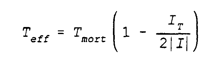
- the corrected instruction should present, depending on whether it is an outgoing current or incoming, level 1 increased or decreased by one time corresponding to a time called "effective time" which would take into account the value of the current.
- T eff T dead
- FIGS. 7 also shows the pace general of the motor currents either in the case where does not apply the method according to the present invention (fig. 7a), either in the case where this process is applied (fig. 7b), for an inverter without snubber.
- FIGS. 8 show the harmonics 5 and 7 on the current side as well as the harmonic 6 on the power supply side, on the one hand in the case where the process is not applied according to the present invention (see figs. 8a and 8b) and other part in the case where this process is applied (figs. 8c and 8d).
Landscapes
- Engineering & Computer Science (AREA)
- Power Engineering (AREA)
- Inverter Devices (AREA)
- Electrical Discharge Machining, Electrochemical Machining, And Combined Machining (AREA)
- Amplifiers (AREA)
- Transmitters (AREA)
- Control Of Motors That Do Not Use Commutators (AREA)
- Dc-Dc Converters (AREA)
- Multi-Process Working Machines And Systems (AREA)
- Crystals, And After-Treatments Of Crystals (AREA)
- Ac-Ac Conversion (AREA)
Description
- La figure 1
- représente une vue schématisée d'une branche d'un onduleur conventionnel à deux niveaux.
- La figure 2
- représente l'onde consigne (fig. 2a) créée par le modulateur pour un onduleur tel que décrit à la figure 1, ainsi que les ondes obtenues à la sortie du discriminateur et destinées à commander directement les commutateurs (fig. 2b et 2c) et les tensions correspondantes appliquées dans ce cas au moteur (fig. 2d et 2e).
- La figure 3
- représente un schéma de principe d'un dispositif permettant la mise en oeuvre du procédé selon l'invention.
- La figure 4
- représente les ondes corrigées (figs. 4b et 4c) pour une onde consigne donnée (fig. 4a) à appliquer à l'onduleur à deux niveaux tel que décrit à la figure 1 afin de mettre en oeuvre le procédé selon la présente invention ainsi que les tensions de sortie appliquées dans ce cas au moteur (figs. 4d et 4e).
- La figure 5
- représente une vue schématisée d'une branche d'un onduleur conventionnel à deux niveaux avec snubber.
- La figure 6
- représente l'onde consigne (fig. 6a) créée par le modulateur et destinée à commander un onduleur tel que décrit à la figure 5, ainsi que les tensions de sortie appliquées dans ce cas au moteur pour un courant entrant faible ou élevé (fig. 6b et 6c) et pour un courant sortant faible ou élevé (fig. 6d et 6e), les fig. 6f et 6g représentant des détails des figures 6b et 6c.
- La figure 7
- représente l'allure générale du courant moteur d'une part en n'appliquant pas le procédé selon la présente invention (fig. 7a) et d'autre part en appliquant ce procédé (fig 7b).
- La figure 8
- représente les harmoniques, et plus particulièrement les harmoniques 5 et 7 côté moteur ainsi que l'harmonique 6 côté alimentation, d'une part lorsque l'on n'applique pas le procédé selon la présente invention (figs. 8a et 8b) et d'autre part lorsque l'on applique ce procédé (figs. 8c et 8d).
Claims (5)
- Procédé de traitement d'ondes PWM destinées à la commande d'un onduleur de tension ou d' un redresseur de tension, cet onduleur ou redresseur comprenant au moins une branche avec au moins une paire de commutateurs (S1, DR1, S2, DR2) reliés en série, par lequel un modulateur crée l'onde de commande PWM sous la forme d'une succession d'états hauts et d'états bas, l'état haut étant défini par le fait que le commutateur relié à la tension la plus positive est fermé tandis que le commutateur relié à la tension la plus négative est ouvert, et l'état bas étant défini par l'inverse, caractérisé en ce que l'onde de commande PWM est corrigée en fonction du sens du courant sortant ou entrant dans la branche de manière à obtenir deux consignes corrigées, la consigne corrigée pour le courant sortant présentant un état haut augmenté d'un délai lors de la transition de l'état haut vers l'état bas, et la consigne corrigée pour le courant entrant présentant un état bas augmenté d'un délai lors de la transition de l'état bas vers l'état haut.
- Procédé selon la revendication 1, caractérisé en ce que le délai introduit dans les consignes corrigées correspond essentiellement au temps mort lui-même introduit par le discriminateur lors de l'opération de fermeture des commutateurs, ceci dans le cas où l'on utilise un onduleur ou un redresseur sans cellule d'aide à la commutation.
- Procédé selon la revendication 1, caractérisé en ce que le délai introduit dans les consignes corrigées dépend non seulement du sens du courant mais également de sa valeur, ceci dans le cas où l'on utilise un onduleur ou un redresseur avec cellule d'aide à la commutation.
- Dispositif pour la mise en oeuvre du procédé de traitement d'ondes PWM selon l'une quelconque des revendications précédentes et qui sont destinées à la commande d' un onduleur de tension ou d'un redresseur de tension, l'onduleur ou redresseur comprenant au moins une branche avec au moins une paire de commutateurs (S1, DR1, S2, DR2) reliés en série, le dispositif comprenant un modulateur créant l'onde de commande PWM sous la forme d'une succession d'états hauts et d'états bas, l'état haut étant défini par le fait que le commutateur relié à la tension la plus positive est fermé tandis que le commutateur relié à la tension la plus négative est ouvert, et l'état bas étant défini par l'inverse, caractérisé en ce que des moyens de correction corrigent l'onde de commande PWM en fonction du sens du courant entrant ou sortant dans la branche de l'onduleur, de manière à créer deux consignes, une consigne corrigée pour le courant sortant présentant un état haut augmenté d'un délai lors de la transition de l'état haut vers l'état bas, et une consigne corrigée pour le courant entrant présentant un état bas augmenté d'un délai lors de la transition de l'état bas vers l'état haut.
- Utilisation du procédé selon l'une quelconque des revendications 1 à 3 ou du dispositif selon la revendication 4 pour un onduleur ou un redresseur commandé de tension avec ou sans cellule d'aide à la commutation, à deux niveaux ou multi-niveaux.
Priority Applications (2)
| Application Number | Priority Date | Filing Date | Title |
|---|---|---|---|
| EP96908936A EP0821844B1 (fr) | 1995-04-21 | 1996-04-12 | Procede de traitement d'ondes pwm et dispositifs appliquant ce procede |
| GR20000401208T GR3033517T3 (en) | 1995-04-21 | 2000-05-26 | Method for processing pwm waves and devices therefor |
Applications Claiming Priority (6)
| Application Number | Priority Date | Filing Date | Title |
|---|---|---|---|
| EP95870040 | 1995-04-21 | ||
| EP95870040 | 1995-04-21 | ||
| EP95870058 | 1995-05-22 | ||
| EP95870058 | 1995-05-22 | ||
| EP96908936A EP0821844B1 (fr) | 1995-04-21 | 1996-04-12 | Procede de traitement d'ondes pwm et dispositifs appliquant ce procede |
| PCT/BE1996/000039 WO1996033548A1 (fr) | 1995-04-21 | 1996-04-12 | Procede de traitement d'ondes pwm et dispositifs appliquant ce procede |
Publications (2)
| Publication Number | Publication Date |
|---|---|
| EP0821844A1 EP0821844A1 (fr) | 1998-02-04 |
| EP0821844B1 true EP0821844B1 (fr) | 2000-03-15 |
Family
ID=26140796
Family Applications (1)
| Application Number | Title | Priority Date | Filing Date |
|---|---|---|---|
| EP96908936A Expired - Lifetime EP0821844B1 (fr) | 1995-04-21 | 1996-04-12 | Procede de traitement d'ondes pwm et dispositifs appliquant ce procede |
Country Status (21)
| Country | Link |
|---|---|
| US (1) | US5991176A (fr) |
| EP (1) | EP0821844B1 (fr) |
| JP (1) | JP3677048B2 (fr) |
| KR (1) | KR100401120B1 (fr) |
| CN (1) | CN1053530C (fr) |
| AT (1) | ATE190777T1 (fr) |
| AU (1) | AU703257B2 (fr) |
| BR (1) | BR9608055A (fr) |
| CA (1) | CA2218738C (fr) |
| CZ (1) | CZ293168B6 (fr) |
| DE (1) | DE69607157T2 (fr) |
| DK (1) | DK0821844T3 (fr) |
| EA (1) | EA000501B1 (fr) |
| ES (1) | ES2144732T3 (fr) |
| GR (1) | GR3033517T3 (fr) |
| HU (1) | HU226738B1 (fr) |
| PL (1) | PL182302B1 (fr) |
| PT (1) | PT821844E (fr) |
| SK (1) | SK141797A3 (fr) |
| TR (1) | TR199701200T1 (fr) |
| WO (1) | WO1996033548A1 (fr) |
Families Citing this family (12)
| Publication number | Priority date | Publication date | Assignee | Title |
|---|---|---|---|---|
| JPH1132481A (ja) * | 1997-07-08 | 1999-02-02 | Media Technol:Kk | スイッチングレギュレータ |
| US6714424B2 (en) | 2001-11-30 | 2004-03-30 | Ballard Power Systems Corporation | Dead-time compensation with narrow pulse elimination in solid- state switch devices |
| US6690135B2 (en) * | 2002-01-24 | 2004-02-10 | Delphi Technologies, Inc. | Method for compensating for dead time non-linearities in a pulse width modulation controlled switching scheme |
| US7239535B2 (en) * | 2004-08-31 | 2007-07-03 | Abb Technology Ltd. | Voltage source converter |
| JP4581574B2 (ja) * | 2004-09-08 | 2010-11-17 | 株式会社ジェイテクト | モータ制御装置及び電動パワーステアリング装置 |
| TW201240298A (en) * | 2011-03-21 | 2012-10-01 | Motech Ind Inc | Inverter for converting a direct current voltage into an alternating current voltage and method thereof |
| US20130193766A1 (en) | 2012-01-31 | 2013-08-01 | Atlantic Grid Operations A., Llc | Control and protection of a dc power grid |
| DE102012206721A1 (de) * | 2012-04-24 | 2013-10-24 | Bayerische Motoren Werke Aktiengesellschaft | Steuern von Schaltelementen einer im Wesentlichen im Gegentakt angesteuerten Halbbrücke in einem Umrichter |
| CN104734474B (zh) * | 2013-12-23 | 2017-07-18 | 立锜科技股份有限公司 | 切换式电源供应器及其控制电路与控制方法 |
| US9960608B2 (en) * | 2016-03-04 | 2018-05-01 | Qualcomm Incorporated | High frequency multi-level rectification |
| DE102020200683A1 (de) | 2020-01-22 | 2021-07-22 | Zf Friedrichshafen Ag | Verfahren zur Steuerung eines Wechselrichters einer elektrischen Maschine für ein Kraftfahrzeug |
| DE102022201487A1 (de) | 2022-02-14 | 2023-08-17 | Zf Friedrichshafen Ag | Verfahren zur Ansteuerung einer Schaltungsanordnung für Leistungshalbleiter |
Family Cites Families (11)
| Publication number | Priority date | Publication date | Assignee | Title |
|---|---|---|---|---|
| CN1013332B (zh) * | 1988-03-06 | 1991-07-24 | 陕西机械学院 | 采用微处理器的脉宽调制逆变器控制装置 |
| US5072354A (en) * | 1989-05-16 | 1991-12-10 | Mitsubishi Denki Kabushiki Kaisha | Pulse-width modulation type inverter apparatus |
| GB2238188B (en) * | 1989-05-16 | 1993-12-22 | Mitsubishi Electric Corp | Pulse-width modulation type inverter apparatus |
| JPH078146B2 (ja) * | 1989-05-23 | 1995-01-30 | 春日電機株式会社 | インバータの制御装置 |
| DE4016286A1 (de) * | 1990-05-21 | 1991-11-28 | Bosch Gmbh Robert | Verfahren zur impulsbreitenmodulation fuer einen umrichter |
| US5436819A (en) * | 1991-07-25 | 1995-07-25 | Mitsubishi Denki Kabushiki Kaisha | Apparatus for and method of compensating for an output voltage error in an inverter output |
| FR2693325B1 (fr) * | 1992-07-03 | 1994-08-26 | Montpellier Ii Universite | Procédé de commande d'interrupteurs, notamment d'interrupteurs bidirectionnels, dispositifs de commande pour la mise en Óoeuvre de ce procédé et convertisseur ainsi commandés. |
| US5450306A (en) * | 1992-12-07 | 1995-09-12 | Square D Company | Closed loop pulse width modulator inverter with volt-seconds feedback control |
| JP2768206B2 (ja) * | 1993-03-30 | 1998-06-25 | 三菱電機株式会社 | インバータ装置 |
| JPH08289561A (ja) * | 1995-02-14 | 1996-11-01 | Toshiba Corp | 電力変換装置 |
| US5646837A (en) * | 1995-12-19 | 1997-07-08 | Performance Controls, Inc. | Pulse-width modulated circuit with improved linearity |
-
1996
- 1996-04-12 JP JP53136096A patent/JP3677048B2/ja not_active Expired - Fee Related
- 1996-04-12 CZ CZ19973219A patent/CZ293168B6/cs not_active IP Right Cessation
- 1996-04-12 KR KR1019970707353A patent/KR100401120B1/ko not_active IP Right Cessation
- 1996-04-12 CA CA002218738A patent/CA2218738C/fr not_active Expired - Lifetime
- 1996-04-12 EP EP96908936A patent/EP0821844B1/fr not_active Expired - Lifetime
- 1996-04-12 DK DK96908936T patent/DK0821844T3/da active
- 1996-04-12 AU AU52625/96A patent/AU703257B2/en not_active Expired
- 1996-04-12 PL PL96323106A patent/PL182302B1/pl unknown
- 1996-04-12 ES ES96908936T patent/ES2144732T3/es not_active Expired - Lifetime
- 1996-04-12 CN CN96193385A patent/CN1053530C/zh not_active Expired - Lifetime
- 1996-04-12 SK SK1417-97A patent/SK141797A3/sk unknown
- 1996-04-12 TR TR97/01200T patent/TR199701200T1/xx unknown
- 1996-04-12 DE DE69607157T patent/DE69607157T2/de not_active Expired - Lifetime
- 1996-04-12 BR BR9608055-8A patent/BR9608055A/pt not_active IP Right Cessation
- 1996-04-12 AT AT96908936T patent/ATE190777T1/de active
- 1996-04-12 US US08/954,864 patent/US5991176A/en not_active Expired - Lifetime
- 1996-04-12 EA EA199700238A patent/EA000501B1/ru not_active IP Right Cessation
- 1996-04-12 WO PCT/BE1996/000039 patent/WO1996033548A1/fr active IP Right Grant
- 1996-04-12 HU HU9900066A patent/HU226738B1/hu unknown
- 1996-04-12 PT PT96908936T patent/PT821844E/pt unknown
-
2000
- 2000-05-26 GR GR20000401208T patent/GR3033517T3/el unknown
Also Published As
| Publication number | Publication date |
|---|---|
| KR100401120B1 (ko) | 2004-12-31 |
| GR3033517T3 (en) | 2000-09-29 |
| PT821844E (pt) | 2000-09-29 |
| MX9708086A (es) | 1998-07-31 |
| TR199701200T1 (xx) | 1998-03-21 |
| AU703257B2 (en) | 1999-03-25 |
| PL323106A1 (en) | 1998-03-16 |
| US5991176A (en) | 1999-11-23 |
| ES2144732T3 (es) | 2000-06-16 |
| DK0821844T3 (da) | 2000-08-21 |
| PL182302B1 (pl) | 2001-12-31 |
| EA000501B1 (ru) | 1999-08-26 |
| CA2218738C (fr) | 2008-10-07 |
| SK141797A3 (en) | 1998-06-03 |
| EP0821844A1 (fr) | 1998-02-04 |
| HUP9900066A2 (hu) | 1999-04-28 |
| KR19990007830A (ko) | 1999-01-25 |
| AU5262596A (en) | 1996-11-07 |
| BR9608055A (pt) | 1999-11-30 |
| HUP9900066A3 (en) | 1999-11-29 |
| JP3677048B2 (ja) | 2005-07-27 |
| CA2218738A1 (fr) | 1996-10-24 |
| HU226738B1 (en) | 2009-08-28 |
| WO1996033548A1 (fr) | 1996-10-24 |
| ATE190777T1 (de) | 2000-04-15 |
| CZ293168B6 (cs) | 2004-02-18 |
| DE69607157T2 (de) | 2000-11-16 |
| DE69607157D1 (de) | 2000-04-20 |
| JPH11503900A (ja) | 1999-03-30 |
| CN1053530C (zh) | 2000-06-14 |
| CZ321997A3 (cs) | 1998-01-14 |
| EA199700238A1 (ru) | 1998-02-26 |
| CN1182507A (zh) | 1998-05-20 |
Similar Documents
| Publication | Publication Date | Title |
|---|---|---|
| EP0821844B1 (fr) | Procede de traitement d'ondes pwm et dispositifs appliquant ce procede | |
| EP2355331B1 (fr) | Dispositif convertisseur et alimentation sans interruption équipée d'un tel dispositif | |
| EP1964257B1 (fr) | Procede de commande d'un onduleur de tension polyphase | |
| FR2744295A1 (fr) | Circuit de protection de dispositifs de commutation de puissance elevee | |
| EP0720281B1 (fr) | Dispositif électronique de conversion de l'énergie électrique | |
| EP0933858A1 (fr) | Procédé de protection par mise en court-circuit | |
| EP3232556A1 (fr) | Procédé et système de commande pour une installation de commande de moteur électrique | |
| EP1964256B1 (fr) | Procede de commande d'un onduleur de tension polyphase | |
| FR2557753A1 (fr) | Dispositif de commande electrique et circuit d'excitation pour charge electrique | |
| WO1981003722A1 (fr) | Onduleur a transistors ou a thyristors a recuperation d'energie | |
| FR2606228A1 (fr) | Dispositif de controle a la sortie d'une unite d'alimentation en courant haute frequence | |
| FR2952483A1 (fr) | Dispositif convertisseur et alimentation sans interruption equipee d'un tel dispositif. | |
| EP1835610A1 (fr) | Procédé de paramétrage d'un convertisseur et convertisseur mettant en oeuvre le procédé | |
| EP0336019B2 (fr) | Modulateur multiniveau en largeur d'impulsion | |
| FR2940863A1 (fr) | Alimentation electrique d'un aeronef | |
| EP0670624B1 (fr) | Alimentation à découpage adaptée pour permettre des commutations sous tension réduite | |
| EP0344067B1 (fr) | Procédé de linéarisation pour convertisseur continu-continu et dispositifs mettant en oeuvre ce procéde | |
| EP0616415A1 (fr) | Dispositif de commande du circuit oscillant d'un onduleur de tension fonctionnant en quasi-résonance à régulation à modulation de largeur d'impulsion | |
| EP2595296B1 (fr) | Système de commande comportant un module onduleur employé comme redresseur actif | |
| EP2182622B1 (fr) | Circuit de correction de facteur de puissance. | |
| CA1211499A (fr) | Circuit de commande d'un moteur synchrone a deux enroulements induits | |
| EP2647112B1 (fr) | Variateur de vitesse equipe d'un dispositif de filtrage de mode commun | |
| EP2293422B1 (fr) | Convertisseur d'un courant continu en un autre courant continu avec imbrication de signaux de commande, et système d'alimentation comprenant un tel convertisseur | |
| CA1108693A (fr) | Onduleur autonome a modulation de largeur d'impulsions | |
| WO2012084572A2 (fr) | Convertisseur de puissance ac/dc a facteur de puissance et thdi ameliores |
Legal Events
| Date | Code | Title | Description |
|---|---|---|---|
| PUAI | Public reference made under article 153(3) epc to a published international application that has entered the european phase |
Free format text: ORIGINAL CODE: 0009012 |
|
| 17P | Request for examination filed |
Effective date: 19970901 |
|
| AK | Designated contracting states |
Kind code of ref document: A1 Designated state(s): AT BE CH DE DK ES FI FR GB GR IE IT LI LU MC NL PT SE |
|
| 17Q | First examination report despatched |
Effective date: 19980326 |
|
| GRAG | Despatch of communication of intention to grant |
Free format text: ORIGINAL CODE: EPIDOS AGRA |
|
| GRAH | Despatch of communication of intention to grant a patent |
Free format text: ORIGINAL CODE: EPIDOS IGRA |
|
| GRAH | Despatch of communication of intention to grant a patent |
Free format text: ORIGINAL CODE: EPIDOS IGRA |
|
| RAP1 | Party data changed (applicant data changed or rights of an application transferred) |
Owner name: ALSTHOM BELGIUM S.A. |
|
| RAP3 | Party data changed (applicant data changed or rights of an application transferred) |
Owner name: ALSTOM BELGIUM S.A. |
|
| GRAA | (expected) grant |
Free format text: ORIGINAL CODE: 0009210 |
|
| AK | Designated contracting states |
Kind code of ref document: B1 Designated state(s): AT BE CH DE DK ES FI FR GB GR IE IT LI LU MC NL PT SE |
|
| REF | Corresponds to: |
Ref document number: 190777 Country of ref document: AT Date of ref document: 20000415 Kind code of ref document: T |
|
| REG | Reference to a national code |
Ref country code: CH Ref legal event code: EP |
|
| REF | Corresponds to: |
Ref document number: 69607157 Country of ref document: DE Date of ref document: 20000420 |
|
| REG | Reference to a national code |
Ref country code: CH Ref legal event code: NV Representative=s name: ABREMA AGENCE BREVETS ET MARQUES GANGUILLET & HUMP |
|
| GBT | Gb: translation of ep patent filed (gb section 77(6)(a)/1977) |
Effective date: 20000410 |
|
| REG | Reference to a national code |
Ref country code: IE Ref legal event code: FG4D Free format text: FRENCH |
|
| ITF | It: translation for a ep patent filed |
Owner name: MARCHI & PARTNERS S.R.L. |
|
| REG | Reference to a national code |
Ref country code: ES Ref legal event code: FG2A Ref document number: 2144732 Country of ref document: ES Kind code of ref document: T3 |
|
| REG | Reference to a national code |
Ref country code: DK Ref legal event code: T3 |
|
| REG | Reference to a national code |
Ref country code: PT Ref legal event code: SC4A Free format text: AVAILABILITY OF NATIONAL TRANSLATION Effective date: 20000615 |
|
| PLBE | No opposition filed within time limit |
Free format text: ORIGINAL CODE: 0009261 |
|
| STAA | Information on the status of an ep patent application or granted ep patent |
Free format text: STATUS: NO OPPOSITION FILED WITHIN TIME LIMIT |
|
| 26N | No opposition filed | ||
| REG | Reference to a national code |
Ref country code: GB Ref legal event code: IF02 |
|
| PGFP | Annual fee paid to national office [announced via postgrant information from national office to epo] |
Ref country code: IE Payment date: 20030408 Year of fee payment: 8 |
|
| PGFP | Annual fee paid to national office [announced via postgrant information from national office to epo] |
Ref country code: MC Payment date: 20030430 Year of fee payment: 8 |
|
| PG25 | Lapsed in a contracting state [announced via postgrant information from national office to epo] |
Ref country code: IE Free format text: LAPSE BECAUSE OF NON-PAYMENT OF DUE FEES Effective date: 20040412 |
|
| PG25 | Lapsed in a contracting state [announced via postgrant information from national office to epo] |
Ref country code: MC Free format text: LAPSE BECAUSE OF NON-PAYMENT OF DUE FEES Effective date: 20040430 |
|
| REG | Reference to a national code |
Ref country code: IE Ref legal event code: MM4A |
|
| PGFP | Annual fee paid to national office [announced via postgrant information from national office to epo] |
Ref country code: LU Payment date: 20100427 Year of fee payment: 15 |
|
| PGFP | Annual fee paid to national office [announced via postgrant information from national office to epo] |
Ref country code: PT Payment date: 20100405 Year of fee payment: 15 Ref country code: FI Payment date: 20100416 Year of fee payment: 15 Ref country code: DK Payment date: 20100413 Year of fee payment: 15 |
|
| PGFP | Annual fee paid to national office [announced via postgrant information from national office to epo] |
Ref country code: SE Payment date: 20100415 Year of fee payment: 15 |
|
| PGFP | Annual fee paid to national office [announced via postgrant information from national office to epo] |
Ref country code: GR Payment date: 20100429 Year of fee payment: 15 |
|
| REG | Reference to a national code |
Ref country code: PT Ref legal event code: MM4A Free format text: LAPSE DUE TO NON-PAYMENT OF FEES Effective date: 20111012 |
|
| REG | Reference to a national code |
Ref country code: SE Ref legal event code: EUG |
|
| REG | Reference to a national code |
Ref country code: GR Ref legal event code: ML Ref document number: 20000401208 Country of ref document: GR Effective date: 20111102 |
|
| PG25 | Lapsed in a contracting state [announced via postgrant information from national office to epo] |
Ref country code: PT Free format text: LAPSE BECAUSE OF NON-PAYMENT OF DUE FEES Effective date: 20111012 Ref country code: FI Free format text: LAPSE BECAUSE OF NON-PAYMENT OF DUE FEES Effective date: 20110412 |
|
| REG | Reference to a national code |
Ref country code: DK Ref legal event code: EBP |
|
| PG25 | Lapsed in a contracting state [announced via postgrant information from national office to epo] |
Ref country code: GR Free format text: LAPSE BECAUSE OF NON-PAYMENT OF DUE FEES Effective date: 20111102 |
|
| PG25 | Lapsed in a contracting state [announced via postgrant information from national office to epo] |
Ref country code: DK Free format text: LAPSE BECAUSE OF NON-PAYMENT OF DUE FEES Effective date: 20110430 |
|
| PG25 | Lapsed in a contracting state [announced via postgrant information from national office to epo] |
Ref country code: SE Free format text: LAPSE BECAUSE OF NON-PAYMENT OF DUE FEES Effective date: 20110413 |
|
| PG25 | Lapsed in a contracting state [announced via postgrant information from national office to epo] |
Ref country code: LU Free format text: LAPSE BECAUSE OF NON-PAYMENT OF DUE FEES Effective date: 20110412 |
|
| REG | Reference to a national code |
Ref country code: FR Ref legal event code: PLFP Year of fee payment: 20 |
|
| PGFP | Annual fee paid to national office [announced via postgrant information from national office to epo] |
Ref country code: NL Payment date: 20150420 Year of fee payment: 20 |
|
| PGFP | Annual fee paid to national office [announced via postgrant information from national office to epo] |
Ref country code: GB Payment date: 20150420 Year of fee payment: 20 Ref country code: DE Payment date: 20150421 Year of fee payment: 20 Ref country code: ES Payment date: 20150417 Year of fee payment: 20 Ref country code: CH Payment date: 20150420 Year of fee payment: 20 |
|
| PGFP | Annual fee paid to national office [announced via postgrant information from national office to epo] |
Ref country code: BE Payment date: 20150420 Year of fee payment: 20 Ref country code: FR Payment date: 20150421 Year of fee payment: 20 Ref country code: AT Payment date: 20150421 Year of fee payment: 20 Ref country code: IT Payment date: 20150427 Year of fee payment: 20 |
|
| REG | Reference to a national code |
Ref country code: DE Ref legal event code: R071 Ref document number: 69607157 Country of ref document: DE |
|
| REG | Reference to a national code |
Ref country code: NL Ref legal event code: MK Effective date: 20160411 |
|
| REG | Reference to a national code |
Ref country code: CH Ref legal event code: PL |
|
| REG | Reference to a national code |
Ref country code: GB Ref legal event code: PE20 Expiry date: 20160411 |
|
| REG | Reference to a national code |
Ref country code: AT Ref legal event code: MK07 Ref document number: 190777 Country of ref document: AT Kind code of ref document: T Effective date: 20160412 |
|
| REG | Reference to a national code |
Ref country code: ES Ref legal event code: FD2A Effective date: 20160727 |
|
| PG25 | Lapsed in a contracting state [announced via postgrant information from national office to epo] |
Ref country code: GB Free format text: LAPSE BECAUSE OF EXPIRATION OF PROTECTION Effective date: 20160411 |
|
| PG25 | Lapsed in a contracting state [announced via postgrant information from national office to epo] |
Ref country code: ES Free format text: LAPSE BECAUSE OF EXPIRATION OF PROTECTION Effective date: 20160413 |