EP0806737A2 - In-system programming with two wire interface - Google Patents
In-system programming with two wire interface Download PDFInfo
- Publication number
- EP0806737A2 EP0806737A2 EP97303091A EP97303091A EP0806737A2 EP 0806737 A2 EP0806737 A2 EP 0806737A2 EP 97303091 A EP97303091 A EP 97303091A EP 97303091 A EP97303091 A EP 97303091A EP 0806737 A2 EP0806737 A2 EP 0806737A2
- Authority
- EP
- European Patent Office
- Prior art keywords
- serial
- interface
- programming
- data
- parallel
- Prior art date
- Legal status (The legal status is an assumption and is not a legal conclusion. Google has not performed a legal analysis and makes no representation as to the accuracy of the status listed.)
- Withdrawn
Links
Images

Classifications
-
- G—PHYSICS
- G06—COMPUTING; CALCULATING OR COUNTING
- G06F—ELECTRIC DIGITAL DATA PROCESSING
- G06F30/00—Computer-aided design [CAD]
- G06F30/30—Circuit design
- G06F30/34—Circuit design for reconfigurable circuits, e.g. field programmable gate arrays [FPGA] or programmable logic devices [PLD]
Definitions
- the present invention relates to the design of programmable logic devices and, in particular, relates to the programming of programmable logic devices.
- an in-system programmable logic device may be reprogrammed in its application without removal from the circuit board.
- ISPLD devices such as those available from Lattice Semiconductor Corporation, Hillsboro, Oregon, can be reprogrammed using an operating power supply rather than a high programming voltage.
- the method of reprogramming an ISPLD in place is known in the art as in-system programming (ISP).
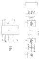
- Figure 1 shows an idealized pin-out of a typical ISPLD 5.
- ISPLD 5 comprises a number of input-only pins (I 1 , I 2 ..., I n ), a number of programmable input/output pins (I/O 1 , I/O 2 ,...,I/O m ), power (VCC) and ground (GND) pins, and a set of four ISP pins (SDI, SDO, SCLK, and MODE).
- a host system including a microprocessor or microcontroller and a signal source (which is well known and thus not shown for simplicity) converts the desired programming parameters into a JEDEC file using a design tool such as Synario/pDS available from Lattice Semiconductor Corporation.
- This JEDEC file is then converted to a binary file such as for instance an ispSTREAM file using software such as JED2ISP Conversion Utility available from Lattice Semiconductor Corporation.
- an isp signal source provides programming data and programming control signals to ISPLD 5 at pins SDI, SCLK, and MODE, respectively, and receives signals from ISPLD 5 indicative of for instance programming verification or self-test at pin SDO.
- an 8-bit parallel port serves as the interface between the host system and ISPLD 5.
- ISPLD 5 is said to employ a four-wire interface.
- ISP mode a state machine within ISPLD 5 having numerous states takes over control of the programming activities.
- Programming data generated by the host system is input serially into the program memory of ISPLD 5 over the serial input pin SDI via the parallel interface.
- the rate of serial input is 1-bit per clock period.
- a clock signal is provided on pin SCLK when the ISP mode is entered.
- Each ISPLD 5 can in a mode operation referred to as Flowthrough mode provide on its output pin SDO data received from its serial input pin SDI. In this manner, a number of ISPLDs 5 may be "daisy-chained" together by tying the serial input pin SDI of one ISPLD 5 to the serial output pin SDO of another ISPLD 5.
- Any ISPLD 5 in the daisy chain can be re-programmed by providing the new program to the serial input pin SDI of the first ISPLD 5, where the data is then provided to the ISPLD 5 desired to be programmed by shifting the data through intervening ISPLDs 5 (which are placed in Flowthrough mode) in the daisy chain.
- ISPLD 5 In-system programming techniques for ISPLDs employing a four-wire ISP parallel interface such as ISPLD 5 are discussed further in U.S. Patents 4,855,954 (entitled “In-system Programmable Logic Device with Four Dedicated Terminals” to Turner et al, issued August 8, 1989), 4,761,768 (entitled “Programmable Logic Device”, to Turner et al, issued August 2, 1988), and 4,896,296 (entitled “Programmable Logic Device Configurable I/O Cell”, to Turner et al, issued Jan 23, 1990).
- ISPLDs reduce total pin overhead by employing only one dedicated programming pin, e.g. the in-system programming or ispEN pin.
- the ISPLD When an enabling signal associated with the ispEN pin is asserted, this ISPLD enters a programming mode.
- the additional in-system programming pins (SDI, SDO, SCLK, and MODE) referred to above are made available by multiplexing pins which are normally, i.e., when not in programming mode, input/output pins. In-system programming may thus be implemented at the cost of only a single dedicated pin.
- programming techniques using only one dedicated programming pin ispEN see U.S.
- Patent 5,237,218 (entitled “Structure and Method for Multiplexing Pins for In-System Programming", to Josephson et al, issued August 17, 1993), hereby incorporated by reference. Note that when ISPLDs having a dedicated programming pin ispEN are in a programming state, the use of five pins (ispEN, SDI, SDO, SCLK, and MODE) are required. Accordingly, such ISPLDs require a five-wire interface.
- a structure and a method to implement programming of an in-system programmable logic device using only a two-wire interface is disclosed.
- program data generated by the host system to be used in programming one or more associated ISPLDs is converted using a first interface from a parallel data format to a serial data string and then transmitted serially to a second interface receiving unit.
- the first and second interfaces employ Universal Asynchronous Receiver/Transmitter (UARTs).
- UARTs Universal Asynchronous Receiver/Transmitter
- the receiving unit converts the serial program data string to a parallel data byte which is then provided to the programming pins of the ISPLD desired to be programmed.
- inventions in accordance with the present invention may utilize a two-wire transmission scheme, and thus two-wire interfaces, to facilitate programming of the associated ISPLDs.
- Having the capability to utilize a two-wire transmission scheme allows ISPLDs in accordance with the present invention to be programmed using wired transmission schemes such as for instance coaxial, twisted pair, and coaxial as wells as wireless transmission schemes such as for instance radio frequency (RF) and infrared radiation (Ir).
- RF radio frequency
- Ir infrared radiation
- Embodiments in accordance with the present invention are discussed below in the context of ISPLD configured in a manner consistent to use five ISP signals during programming (i.e. ISP enable, serial data in, serial data out, mode, and shift clock) at associated respective pins ispEN, SDI, SDO, MODE, and SCLK. It is to be noted, however, that those skilled in the art will, after reading the disclosure below, be readily able to apply the teachings herein to ISPLDs utilizing a different number of ISP programming signals and/or pins during programming, such as for instance the four-wire ISPLD 5 of Figure 1.
- ISPLD 40 shown in Figure 2 and discussed below is representative of any suitable PLD, including those employing EPROM, EEPROM, and Flash memory cells.
- EPROM erasable programmable read-only memory
- EEPROM electrically erasable read-only memory
- Flash memory cells For convenience, those elements common to various illustrative embodiments discussed below are similarly labelled.
- an ISP signal source 10 contained in a suitable host system such as for instance a PC or UNIX machine generates the programming signals associated with pins ispEN, SDI, SCLK, and MODE of an ISPLD 40 in a well known manner.
- These signals are provided in parallel format e.g. a parallel byte to an interface 20 via a five-wire interface bus 11 which may in other embodiments include a greater number of wires.
- Interface 20 converts this parallel byte to a half duplex or full duplex serial data string, and then transmits this serial data string to a half duplex or full duplex interface 30 via one line 21 of a two-wire serial transmission interface 21, 22.
- Interface 30 receives the serial string and converts the serial data string into parallel form and, in this manner, provides the ISP programming signals to respective pins ispEN, SDI, SCLK, and MODE of ISPLD 40 via five-wire interface bus 31, which in other embodiments may include a greater number of wires.
- Signals indicative of information relating to the operation of ISPLD 40 may be provided from ISPLD 40 to interface 30 as serial data on pin SDO.
- Interface 30 converts the serial data string associated with pin SDO of ISPLD 40 into a serial format consistent with that employed in transmitting data from interface 20 to interface 30 via wire 21. This conversion ensures that data may be transmitted from both interface 20 to interface 30 and from interface 30 to interface 20 according to the same transmission protocol.
- this serial data string indicative of the signals at pin SDO is transmitted to interface 20 via another line 22 of the aforementioned serial transmission interface 21, 22. Once received by interface 20, the serial data stream is converted to parallel format and provided to signal source 10 via bus 11.
- the above described embodiment allows ISPLD 40 to be programmed and/or reprogrammed using only a two-wire transmission scheme.
- Present embodiments by allowing ISPLDs 40 to be programmed and/or reprogrammed using a two-wire transmission scheme, are thus able to take advantage of not only various superior two-wire serial transmission schemes such as coaxial, ethernet, conventional phone lines, and fiber optics but also wireless transmission schemes such as infrared and RF.
- two-wire transmission schemes in accordance with the present invention reduce the programming interface pin overhead on the PLD while allowing for increased programming flexibility (i.e., programming via network, remote programming via telephone etc, and wireless programming of system where physical connections between the host system and ISPLD 40 is not feasible).
- interfaces 20 and 30 each employ a Universal Asynchronous Receiver/Transmitter (UART). Signals to be provided to ISPLD 40 may be transmitted between interfaces 20 and 30 according to the RS-232C standard transmission protocol which requires a start bit, 8 data bits, and one stop bit, although other serial transmission protocols may be used. Interfaces 20 and 30 also include a well-known logic circuit which detects when data is received, pauses a predetermined amount of time before transmitting data, and commences the transmission of data. This logic circuit may be in the form of a discrete logic circuit attached to the UART, or in some embodiments may be an ISPLD from Lattice Semiconductor which has been programmed or integrated into a circuit to implement such transmission protocol control functions.
- UART Universal Asynchronous Receiver/Transmitter
- interfaces 20 and 30 may include an Intel 8051 microprocessor having built-in UART capabilities. Employing an 8051 processor in such a manner allows interfaces 20 and 30 to implement additional functions such as variable transmission rates for multiple interfaces. Note that in yet other embodiments other well known techniques may be employed in interfaces 20 and 30 to convert parallel data into a serial data string and to convert a serial data string into parallel data.
- programming ISPLD 40 When programming ISPLD 40, programming data generated by signal source 10 is grouped into data strings for serial transmission by interface 20. For each possible transition on one of the programming pins ispEN, SDI, SDO, SCLK, and MODE, a corresponding data string is loaded into a serial shift register within interface 20 and then serially transmitted to interface 30. In response thereto, interface 30 captures the data string and latches the data string in its parallel register. The time delay typically associated with latching the programming data in the parallel register allows ISPLD 40, or in some embodiments an attached daisy chain of ISPLDs 40, to respond to the signals associated with the next program data string.
- ISPLD 40 Data indicative of ISPLD 40's current status such as for instance self-test results or programming verification is provided to interface 30 by ISPLD 40 via pin SDO.
- Interface 30 converts this data to a serial data stream and transmits this data stream to the host system e.g. signal source 10 in a manner consistent with that discussed above.
- signal source 10 causes the next segment of data to be transmitted to ISPLD 40.
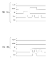
- the timing diagrams shown in Figures 3A and 3B illustrate the relationship between the signals associated with pins ispEN, MODE, SDI, SCLK, and SDO when transmitting and receiving, respectively, serial data.
- Figure 3A illustrates segmenting parallel data for serial transmission to ISPLD 40, where the signals on pins MODE and SDI are clocked by the signal on pin SCLK.
- Figure 3B illustrates segmenting parallel data from ISPLD 40 for serial transmission back to signal source 10 for verification. The data on pins SDO is clocked by the signal on pin SCLK.
- interface 30 may be implemented within ISPLD 40, thereby eliminating the need for a serial controller on the board associated with ISPLD40.
- ISPLD 40 would require a serial port, a serial to parallel register, a parallel to serial register, and a well-known logic circuit to control the transmission of data signals to and from interface 20.
- ISPLDs 40 contained on a single board may be independently programmed by individually selecting and enabling each of ISPLDs 40.
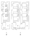
- Figure 4 shows such a board 45 containing interface 30 and three ISPLDs 40.
- Interface 30 may employ a standard 8-bit port to connect with the programming pins of the three ISPLDs 40 contained on board 45, where only seven of the eight pins of the parallel port are used: four of the eight bits of the parallel port are connected to each of respective pins SDI, SDO, MODE, and SCLK of the three ISPLDs 40, and three of the eight bits of the parallel port are individually connected to the ispEN pin of an associated one of ISPLDs 40, as shown in Figure 4, so that each of ISPLDs 40 may be individually enabled for programming via its ispEN pin.
- the remaining pin of the parallel port may be used to enable a fourth ISPLD 40 (not shown) on board 45 or, in other embodiments, may be reserved for other suitable purposes.
- ISPLD 40 (not shown) on board 45 or, in other embodiments, may be reserved for other suitable purposes.
- up to four different ISPLDs 40 may be addressed by the host system.
- the parallel port definition may be as follows: Table 1 pin number pin assignment description send receive 0 SDI/TDI serial data in/text data in 1 MODE/TMS SDO/TDO control mode/test mode select for sending data to ISPLD 40; serial data out/test data out for receiving data from ISPLD 40 2 SCLK/TCK serial clock/test clock 3 ispEN0 enable first ISPLD 40 for ISP 4 ispEN1 enable second ISPLD 40 for ISP 5 ispEN2 enable third ISPLD 40 for ISP 6 ispEN3 enable fourth ISPLD 40 for ISP 7 ispEN4 enable fifth ISPLD 40 for ISP
- TDI, TMS, TDO, and TCK are common to JTAG and Boundary Scan Test Access Port (TAP) used for in-system programming, and is therefore provided in Table 1 for clarity and convenience. Note that any of the pins listed above in Table 1 may be used for both sending and receiving data, as illustrated above by pin 1.
- a daisy chain of ISPLDs 40 may be programmed using the above described serial interfaces in conjunction with software such as ispCODE.C or ispCODE.EXE available from Lattice Semiconductor Corporation.
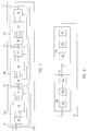
- Figure 5 shows a board 50 including a daisy chain of three ISPLDs 40a-40c and interface 30, although in actual embodiments a greater or fewer number of ISPLDs 40 may be included on board 45.
- ISPLDs 40a-40c are identical to ISPLD 40 discussed above.
- Three of the pins of interface 30 are connected to respective pins SCLK, MODE, and ispEN of ISPLDs 40a-40c.
- a fourth pin of interface 30 is connected to the SDI pin of the first ISPLD 40a.
- the SDO pin of ISPLD 40a is connected to the SDI pin of ISPLD 40b
- the SDO pin of ISPLD 40b is connected to the SDI pin of ISPLD 40c
- the SDO pins of ISPLD 40c is connected to a fifth pin of interface 30.
- interface 30 includes an eight-bit parallel port
- the remaining three bits may be used for controlling multiple daisy chains of ISPLDs 40. Accordingly, when programming a daisy chain such as that shown in Figure 5 in accordance with the present invention, the parallel port definition of interface 30 must be changed from that shown in Table 1 to a well known standard parallel format.
- the signal associated with the ispEN pins of ISPLDs 40 is asserted so as to enable all ISPLDs 40 in the daisy chain.
- the first ISPLD 40a is then addressed and programmed as described above while remaining ISPLDs 40b and 40c are held in a Flowthrough or Bypass mode.
- the SDI/TDI pin of ISPLD 40 is connected directly to its SDO/TDO pin.
- the SDI/TDI pin of ISPLD 40 When in Bypass mode, the SDI/TDI pin of ISPLD 40 is connected to the input terminal of an edge triggered D-type register (not shown for simplicity) and the SDO/TDO pin of the ISPLD 40 is connected to the output terminal of the D-type register.
- Flowthrough and Bypass modes may be enabled either by a specific instruction provided to ISPLD 40 or by a combination of signals provided on the programming pins of ISPLD 40.
- the first ISPLD 40a in the daisy chain After having been programmed, the first ISPLD 40a in the daisy chain is placed in Flowthrough or Bypass mode while the second ISPLD 40b in the daisy chain is programmed, and so on until all ISPLDs 40a-40c in the daisy chain have been programmed.
- multiple ISPLDs 40 may be programmed in parallel to reduce programming time.
- the programming software operating within the host system must support parallel programming.
- software such as DDOWNLD.EXE, WDOWNLD.EXE, ispATE.EXE and ispCODE.EXE (collectively known in the industry as Turbo programming) available from Lattice Semiconductor Corporation supports parallel programming and may thus be used.
- Turbo programming available from Lattice Semiconductor Corporation supports parallel programming and may thus be used.
- the daisy chain of ISPLDs 40 is treated as a single device.
- each of the ISPLDs 40 in the daisy chain is clocked to a shift state.
- a Data Shift command is then provided to ISPLDs 40, after which programming data for ISPLDs 40 is sequentially clocked into the data registers of ISPLDs 40 via their respective SDI pins.
- the ISPLDs 40 then enter the Data Shift State.
- the Program Data command is then clocked into the ISPLDs 40 of the daisy chain, after which the ISPLDs 40 enter the Execute state.
- a clock pulse asserted on pin SCLK causes data stored in the shift registers of ISPLDs 40 to program the EEPROM cells within ISPLDs 40, thereby reprogramming ISPLDs 40.
- the required programming pulse width time delay is applied to transfer sufficient electrons to the floating gate of the EEPROM cell. Once the required programming pulse width time delay (TPWP) has been applied a clock pulse to halt programming and clock back to the Shift State is asserted. This process continues until the entire daisy chain of ISPLDs 40 is programmed.
- Each interface 30 shown in Figure 6 includes a well-known decoder logic circuit which, upon detecting that its assigned address code has been asserted by the host system, enables its internal serial controller (not shown for simplicity) for programming. The enabled interface 30 then facilitates programming of ISPLDs 40 associated therewith. Those interfaces 30 not addressed by the host system are disabled and therefore inactive.
- the host system disables that interface 30 and then addresses interface 30 associated with another board e.g. board 50b, thereby allowing programming of another corresponding daisy chain of ISPLDs 40.
- FIG. 7 shows three such device 70a-70c formed on a board 72, where two-wire serial transmission interface 21, 22 is connected to and provides programming signals to a first one of devices 70a via its interface 30.
- This interface 30 is connected to an associated ISPLD 40 in the manner described above with respect to Figure 2.
- a configuration having a greater number of wires such as for instance a standard 8-bit parallel port may be employed.
- the host system When programming ISPLDs 40 shown in the embodiment of Figure 7, the host system provides programming data to interface 30 of board 70a as discussed above with respect to Figure 2.
- the serial program data string is received by this interface 30, converted to parallel format, and provided to its associated ISPLD 40.
- the associated ISPLD 40 transmits the program data in parallel to its associated interface 20 which, as discussed above, converts the program data to a serial data string.
- the program data is transmitted via single wire 21 to a second one of devices 70b, where the serial string is received and converted to parallel format by its interface 30.
- Data indicative of each of ISPLDs 40 current status such as for instance self-test results or programming verification is provided to the host device via wire 22.
- board 72 is shown in Figure 7 to include only three of devices 70a-70c, board 72 may in actual embodiments include a greater or fewer number of devices 70. Further, any number of boards 72 may be connected together, as shown for instance in Figure 8, and programmed as discussed above.
- a direct physical connection is made between the host computer and PC board containing one or more ISPLDs 40.
- This physical connection may be for instance a twisted pair which allows for two-wire testing and programming of ISPLD(s) provided on the board, thereby saving valuable pin resources of ISPLD(s) 40 provided on the board.
- Transmitting serial data in a manner consistent with a two-wire transmission scheme advantageously allows phone lines to be used in such transmissions.
- modems may be coupled in a well known manner to interfaces 20 and 30, thereby allowing programming data to be used in programming ISPLD 40 to be transmitted over long distances using phone lines rather than transmission wires 21, 22. This feature is especially useful in remote environments such as when field upgrading a board or system of ISPLDs 40.
- Wireless transmission schemes may also be used instead of two-wire serial transmission interface 21, 22 shown for instance in Figure 2.
- RF Radio Frequency
- Infrared (IR) technology may also be used in accordance with the present invention to transmit program data from the host system to a board containing ISPLDs 40 desired to be programmed.
- IR transmission of program data may be implemented by simply coupling an Infrared Data Association (IrDA) standards compliant transmitter to the host system and coupling an IrDA standards compliant receiver to the board in a well-known manner.
- the IrDA transmitter may be initialized by the host system and the IrDA receiver may be initialized by a well known logic circuit coupled thereto. As long as both the receiver and transmitter are initialized to utilize the same data transmitter rate, other wireless transmission protocols may be employed.
Abstract
Program data generated by the host system to be used in programming one or more associated ISPLDs is converted using a first interface from a parallel data format to a serial data string and then transmitted serially to a second interface. In one embodiment, the first and second interfaces employ Universal Asynchronous Receiver/Transmitter (UARTs). The receiving unit converts the serial program data string to a parallel data byte which is then provided to the programming pins of the ISPLD desired to be programmed. Signals indicative of information relating to the operation of one or more of the ISPLDs associated with the host system may be provided to the host system via pin SDO of the asserted ISPLD. In this manner, embodiments in accordance with the present invention may utilize a two-wire transmission scheme, and thus two-wire interfaces, to facilitate programming of the associated ISPLDs. Having the capability to utilize a two-wire transmission scheme, in turn, allows ISPLDs in accordance with the present invention to be programmed using wired transmission schemes such as for instance coaxial, twisted pair, and coaxial as wells as wireless transmission schemes such as for instance radio frequency (RF) and infrared radiation (Ir).
Description
- The present invention relates to the design of programmable logic devices and, in particular, relates to the programming of programmable logic devices.
- Unlike a conventional programmable logic device, an in-system programmable logic device (ISPLD) may be reprogrammed in its application without removal from the circuit board. Some ISPLD devices, such as those available from Lattice Semiconductor Corporation, Hillsboro, Oregon, can be reprogrammed using an operating power supply rather than a high programming voltage. The method of reprogramming an ISPLD in place is known in the art as in-system programming (ISP). Figure 1 shows an idealized pin-out of a
typical ISPLD 5. As shown in Figure 1,ISPLD 5 comprises a number of input-only pins (I1, I2 ..., In), a number of programmable input/output pins (I/O1, I/O2,...,I/Om), power (VCC) and ground (GND) pins, and a set of four ISP pins (SDI, SDO, SCLK, and MODE). - To reprogram ISPLD 5 using ISP, a host system including a microprocessor or microcontroller and a signal source (which is well known and thus not shown for simplicity) converts the desired programming parameters into a JEDEC file using a design tool such as Synario/pDS available from Lattice Semiconductor Corporation. This JEDEC file is then converted to a binary file such as for instance an ispSTREAM file using software such as JED2ISP Conversion Utility available from Lattice Semiconductor Corporation. In response to this ispSTREAM file, an isp signal source provides programming data and programming control signals to
ISPLD 5 at pins SDI, SCLK, and MODE, respectively, and receives signals fromISPLD 5 indicative of for instance programming verification or self-test at pin SDO. Typically, where for example the host system is a PC-based machine, an 8-bit parallel port serves as the interface between the host system andISPLD 5. In such cases, where only four of the 8-bits of the parallel port are utilized, ISPLD 5 is said to employ a four-wire interface. - In the ISP mode, a state machine within ISPLD 5 having numerous states takes over control of the programming activities. Programming data generated by the host system is input serially into the program memory of
ISPLD 5 over the serial input pin SDI via the parallel interface. The rate of serial input is 1-bit per clock period. A clock signal is provided on pin SCLK when the ISP mode is entered. EachISPLD 5 can in a mode operation referred to as Flowthrough mode provide on its output pin SDO data received from its serial input pin SDI. In this manner, a number ofISPLDs 5 may be "daisy-chained" together by tying the serial input pin SDI of oneISPLD 5 to the serial output pin SDO of anotherISPLD 5. AnyISPLD 5 in the daisy chain can be re-programmed by providing the new program to the serial input pin SDI of thefirst ISPLD 5, where the data is then provided to theISPLD 5 desired to be programmed by shifting the data through intervening ISPLDs 5 (which are placed in Flowthrough mode) in the daisy chain. - In-system programming techniques for ISPLDs employing a four-wire ISP parallel interface such as
ISPLD 5 are discussed further in U.S. Patents 4,855,954 (entitled "In-system Programmable Logic Device with Four Dedicated Terminals" to Turner et al, issued August 8, 1989), 4,761,768 (entitled "Programmable Logic Device", to Turner et al, issued August 2, 1988), and 4,896,296 (entitled "Programmable Logic Device Configurable I/O Cell", to Turner et al, issued Jan 23, 1990). - More recent ISPLDs reduce total pin overhead by employing only one dedicated programming pin, e.g. the in-system programming or ispEN pin. When an enabling signal associated with the ispEN pin is asserted, this ISPLD enters a programming mode. The additional in-system programming pins (SDI, SDO, SCLK, and MODE) referred to above are made available by multiplexing pins which are normally, i.e., when not in programming mode, input/output pins. In-system programming may thus be implemented at the cost of only a single dedicated pin. For a more detailed explanation of programming techniques using only one dedicated programming pin ispEN, see U.S. Patent 5,237,218 (entitled "Structure and Method for Multiplexing Pins for In-System Programming", to Josephson et al, issued August 17, 1993), hereby incorporated by reference. Note that when ISPLDs having a dedicated programming pin ispEN are in a programming state, the use of five pins (ispEN, SDI, SDO, SCLK, and MODE) are required. Accordingly, such ISPLDs require a five-wire interface.
- It is thus desirable to implement a system capable of providing program data to and receive response data from a PLD using a two-wire transmission means. In this manner, transmission techniques such as standard telephone lines and wireless communications may be employed to remotely program the ISPLD.
- A structure and a method to implement programming of an in-system programmable logic device using only a two-wire interface is disclosed. In accordance with the present invention, program data generated by the host system to be used in programming one or more associated ISPLDs is converted using a first interface from a parallel data format to a serial data string and then transmitted serially to a second interface receiving unit. In one embodiment, the first and second interfaces employ Universal Asynchronous Receiver/Transmitter (UARTs). The receiving unit converts the serial program data string to a parallel data byte which is then provided to the programming pins of the ISPLD desired to be programmed. Signals indicative of information relating to the operation of one or more of the ISPLDs associated with the host system such as for instance device self-tests and verification of programming may be provided to the host system via pin SDO. Thus, embodiments in accordance with the present invention may utilize a two-wire transmission scheme, and thus two-wire interfaces, to facilitate programming of the associated ISPLDs. Having the capability to utilize a two-wire transmission scheme, in turn, allows ISPLDs in accordance with the present invention to be programmed using wired transmission schemes such as for instance coaxial, twisted pair, and coaxial as wells as wireless transmission schemes such as for instance radio frequency (RF) and infrared radiation (Ir).
-
- Figure 1 is an idealized pin-out diagram of a conventional in-system programmable logic device (ISPLD) having dedicated programming pins SDI, SDO, SCLK, and MODE;
- Figure 2 is a block diagram of an interface system including an ISPLD in accordance with one embodiment of the present invention;
- Figures 3A and 3B are timing diagrams illustrating signals associated with various programming pins of an ISPLD during the transmission of serial data to an ISPLD and the reception of serial data from an ISPLD in accordance with the present invention, respectively; and
- Figures 4-8 are block diagrams illustrating various programming schemes in accordance with the present invention.
- Embodiments in accordance with the present invention are discussed below in the context of ISPLD configured in a manner consistent to use five ISP signals during programming (i.e. ISP enable, serial data in, serial data out, mode, and shift clock) at associated respective pins ispEN, SDI, SDO, MODE, and SCLK. It is to be noted, however, that those skilled in the art will, after reading the disclosure below, be readily able to apply the teachings herein to ISPLDs utilizing a different number of ISP programming signals and/or pins during programming, such as for instance the four-
wire ISPLD 5 of Figure 1. Further, it is to be understood that theISPLD 40 shown in Figure 2 and discussed below is representative of any suitable PLD, including those employing EPROM, EEPROM, and Flash memory cells. For convenience, those elements common to various illustrative embodiments discussed below are similarly labelled. - Referring now to Figure 2, an
ISP signal source 10 contained in a suitable host system such as for instance a PC or UNIX machine generates the programming signals associated with pins ispEN, SDI, SCLK, and MODE of anISPLD 40 in a well known manner. These signals are provided in parallel format e.g. a parallel byte to aninterface 20 via a five-wire interface bus 11 which may in other embodiments include a greater number of wires.Interface 20 converts this parallel byte to a half duplex or full duplex serial data string, and then transmits this serial data string to a half duplex orfull duplex interface 30 via oneline 21 of a two-wireserial transmission interface Interface 30, in turn, receives the serial string and converts the serial data string into parallel form and, in this manner, provides the ISP programming signals to respective pins ispEN, SDI, SCLK, and MODE ofISPLD 40 via five-wire interface bus 31, which in other embodiments may include a greater number of wires. - Signals indicative of information relating to the operation of
ISPLD 40 such as for instance device self-tests and verification of programming may be provided from ISPLD 40 to interface 30 as serial data on pin SDO.Interface 30 converts the serial data string associated with pin SDO ofISPLD 40 into a serial format consistent with that employed in transmitting data frominterface 20 tointerface 30 viawire 21. This conversion ensures that data may be transmitted from bothinterface 20 tointerface 30 and frominterface 30 tointerface 20 according to the same transmission protocol. Once converted, this serial data string indicative of the signals at pin SDO is transmitted tointerface 20 via anotherline 22 of the aforementionedserial transmission interface interface 20, the serial data stream is converted to parallel format and provided tosignal source 10 viabus 11. - Thus, unlike conventional programming schemes for ISPLDs which require a transmission means having a minimum of four or five wires, the above described embodiment allows ISPLD 40 to be programmed and/or reprogrammed using only a two-wire transmission scheme. Present embodiments, by allowing ISPLDs 40 to be programmed and/or reprogrammed using a two-wire transmission scheme, are thus able to take advantage of not only various superior two-wire serial transmission schemes such as coaxial, ethernet, conventional phone lines, and fiber optics but also wireless transmission schemes such as infrared and RF. Further, two-wire transmission schemes in accordance with the present invention reduce the programming interface pin overhead on the PLD while allowing for increased programming flexibility (i.e., programming via network, remote programming via telephone etc, and wireless programming of system where physical connections between the host system and ISPLD 40 is not feasible).
- In some embodiments,
interfaces interfaces Interfaces - In other embodiments, interfaces 20 and 30 may include an Intel 8051 microprocessor having built-in UART capabilities. Employing an 8051 processor in such a manner allows
interfaces interfaces - When programming
ISPLD 40, programming data generated bysignal source 10 is grouped into data strings for serial transmission byinterface 20. For each possible transition on one of the programming pins ispEN, SDI, SDO, SCLK, and MODE, a corresponding data string is loaded into a serial shift register withininterface 20 and then serially transmitted tointerface 30. In response thereto,interface 30 captures the data string and latches the data string in its parallel register. The time delay typically associated with latching the programming data in the parallel register allowsISPLD 40, or in some embodiments an attached daisy chain of ISPLDs 40, to respond to the signals associated with the next program data string. Data indicative of ISPLD 40's current status such as for instance self-test results or programming verification is provided to interface 30 byISPLD 40 via pin SDO.Interface 30 converts this data to a serial data stream and transmits this data stream to the host system e.g. signalsource 10 in a manner consistent with that discussed above. Once the data is received at the host system, signalsource 10 causes the next segment of data to be transmitted to ISPLD 40. The timing diagrams shown in Figures 3A and 3B illustrate the relationship between the signals associated with pins ispEN, MODE, SDI, SCLK, and SDO when transmitting and receiving, respectively, serial data. Figure 3A illustrates segmenting parallel data for serial transmission to ISPLD 40, where the signals on pins MODE and SDI are clocked by the signal on pin SCLK. Figure 3B illustrates segmenting parallel data fromISPLD 40 for serial transmission back to signalsource 10 for verification. The data on pins SDO is clocked by the signal on pin SCLK. - In some embodiments,
interface 30 may be implemented withinISPLD 40, thereby eliminating the need for a serial controller on the board associated with ISPLD40. In such embodiments,ISPLD 40 would require a serial port, a serial to parallel register, a parallel to serial register, and a well-known logic circuit to control the transmission of data signals to and frominterface 20. -
Numerous ISPLDs 40 contained on a single board may be independently programmed by individually selecting and enabling each of ISPLDs 40. Figure 4 shows such aboard 45 containinginterface 30 and three ISPLDs 40.Interface 30 may employ a standard 8-bit port to connect with the programming pins of the threeISPLDs 40 contained onboard 45, where only seven of the eight pins of the parallel port are used: four of the eight bits of the parallel port are connected to each of respective pins SDI, SDO, MODE, and SCLK of the threeISPLDs 40, and three of the eight bits of the parallel port are individually connected to the ispEN pin of an associated one ofISPLDs 40, as shown in Figure 4, so that each of ISPLDs 40 may be individually enabled for programming via its ispEN pin. The remaining pin of the parallel port may be used to enable a fourth ISPLD 40 (not shown) onboard 45 or, in other embodiments, may be reserved for other suitable purposes. Thus, in those embodiments whereinterface 30 includes 8 wires e.g. employs an 8-bit parallel port, up to fourdifferent ISPLDs 40 may be addressed by the host system. In some embodiments, where for instance fivedifferent ISPLDs 40 are addressed, the parallel port definition may be as follows:Table 1 pin number pin assignment description send receive 0 SDI/TDI serial data in/text data in 1 MODE/TMS SDO/TDO control mode/test mode select for sending data to ISPLD 40; serial data out/test data out for receiving data from ISPLD 402 SCLK/TCK serial clock/test clock 3 ispEN0 enable first ISPLD 40 for ISP 4 ispEN1 enable second ISPLD 40 forISP 5 ispEN2 enable third ISPLD 40 for ISP 6 ispEN3 enable fourth ISPLD 40 for ISP 7 ispEN4 enable fifth ISPLD 40 for ISP - The terminology TDI, TMS, TDO, and TCK is common to JTAG and Boundary Scan Test Access Port (TAP) used for in-system programming, and is therefore provided in Table 1 for clarity and convenience. Note that any of the pins listed above in Table 1 may be used for both sending and receiving data, as illustrated above by
pin 1. - Note that in embodiments where it is desired to individually select
ISPLDs 40 on a single board, the programming software operating within the host device must be updated. A sample algorithm which may be used by the programming software operating in the host system is provided below. It is to be understood that this algorithm provided below is illustrative and that other suitable methods may be employed.
- A daisy chain of ISPLDs 40 may be programmed using the above described serial interfaces in conjunction with software such as ispCODE.C or ispCODE.EXE available from Lattice Semiconductor Corporation. Figure 5 shows a
board 50 including a daisy chain of threeISPLDs 40a-40c andinterface 30, although in actual embodiments a greater or fewer number ofISPLDs 40 may be included onboard 45. Note that ISPLDs 40a-40c are identical to ISPLD 40 discussed above. Three of the pins ofinterface 30 are connected to respective pins SCLK, MODE, and ispEN ofISPLDs 40a-40c. A fourth pin ofinterface 30 is connected to the SDI pin of thefirst ISPLD 40a. The SDO pin ofISPLD 40a is connected to the SDI pin ofISPLD 40b, the SDO pin ofISPLD 40b is connected to the SDI pin ofISPLD 40c, and the SDO pins ofISPLD 40c is connected to a fifth pin ofinterface 30. Whereinterface 30 includes an eight-bit parallel port, the remaining three bits may be used for controlling multiple daisy chains of ISPLDs 40. Accordingly, when programming a daisy chain such as that shown in Figure 5 in accordance with the present invention, the parallel port definition ofinterface 30 must be changed from that shown in Table 1 to a well known standard parallel format. - Where it is desired to program one or more of
ISPLDs 40a-40c, the signal associated with the ispEN pins of ISPLDs 40 is asserted so as to enable allISPLDs 40 in the daisy chain. Thefirst ISPLD 40a is then addressed and programmed as described above while remainingISPLDs ISPLD 40 is connected directly to its SDO/TDO pin. When in Bypass mode, the SDI/TDI pin ofISPLD 40 is connected to the input terminal of an edge triggered D-type register (not shown for simplicity) and the SDO/TDO pin of theISPLD 40 is connected to the output terminal of the D-type register. Flowthrough and Bypass modes may be enabled either by a specific instruction provided to ISPLD 40 or by a combination of signals provided on the programming pins ofISPLD 40. After having been programmed, thefirst ISPLD 40a in the daisy chain is placed in Flowthrough or Bypass mode while thesecond ISPLD 40b in the daisy chain is programmed, and so on until allISPLDs 40a-40c in the daisy chain have been programmed. - In other embodiments,
multiple ISPLDs 40 may be programmed in parallel to reduce programming time. In such embodiments, the programming software operating within the host system must support parallel programming. For example, software such as DDOWNLD.EXE, WDOWNLD.EXE, ispATE.EXE and ispCODE.EXE (collectively known in the industry as Turbo programming) available from Lattice Semiconductor Corporation supports parallel programming and may thus be used. When programming a daisy chain ofmultiple ISPLDs 40 in parallel, the daisy chain of ISPLDs 40 is treated as a single device. During programming, each of theISPLDs 40 in the daisy chain is clocked to a shift state. A Data Shift command is then provided to ISPLDs 40, after which programming data forISPLDs 40 is sequentially clocked into the data registers ofISPLDs 40 via their respective SDI pins. The ISPLDs 40 then enter the Data Shift State. The Program Data command is then clocked into theISPLDs 40 of the daisy chain, after which theISPLDs 40 enter the Execute state. A clock pulse asserted on pin SCLK causes data stored in the shift registers ofISPLDs 40 to program the EEPROM cells withinISPLDs 40, thereby reprogrammingISPLDs 40. The required programming pulse width time delay is applied to transfer sufficient electrons to the floating gate of the EEPROM cell. Once the required programming pulse width time delay (TPWP) has been applied a clock pulse to halt programming and clock back to the Shift State is asserted. This process continues until the entire daisy chain of ISPLDs 40 is programmed. -
Multiple boards interface 30 and a chain of ISPLDs 40 may be coupled to one another as shown in Figure 6 and programmed in accordance with the present invention. Note that although discussed below with reference to Figure 6, the teachings of the present invention may be easily adapted to simultaneously program a greater number ofconnected boards 50 each having a fewer or greater number of ISPLDs 40. Eachinterface 30 shown in Figure 6 includes a well-known decoder logic circuit which, upon detecting that its assigned address code has been asserted by the host system, enables its internal serial controller (not shown for simplicity) for programming. The enabledinterface 30 then facilitates programming ofISPLDs 40 associated therewith. Those interfaces 30 not addressed by the host system are disabled and therefore inactive. OnceISPLDs 40 associated with the enabledinterface 30e.g. board 50a have been programmed, the host system disables thatinterface 30 and then addressesinterface 30 associated with anotherboard e.g. board 50b, thereby allowing programming of another corresponding daisy chain of ISPLDs 40. - Multiple
devices including interfaces ISPLD 40 may be connected in a serial fashion and programmed in accordance with the present invention. Figure 7 shows threesuch device 70a-70c formed on aboard 72, where two-wireserial transmission interface devices 70a via itsinterface 30. Thisinterface 30 is connected to an associatedISPLD 40 in the manner described above with respect to Figure 2. Thus, although shown in Figure 7 to employ a five-wire configuration in connectinginterface 30 to the programming pins of ISPLD 40 ofboard 70a, it is to be understood that a configuration having a greater number of wires such as for instance a standard 8-bit parallel port may be employed. - When programming ISPLDs 40 shown in the embodiment of Figure 7, the host system provides programming data to interface 30 of
board 70a as discussed above with respect to Figure 2. The serial program data string is received by thisinterface 30, converted to parallel format, and provided to its associatedISPLD 40. After a specific time delay, the associatedISPLD 40 transmits the program data in parallel to its associatedinterface 20 which, as discussed above, converts the program data to a serial data string. Once converted to a serial string, the program data is transmitted viasingle wire 21 to a second one ofdevices 70b, where the serial string is received and converted to parallel format by itsinterface 30. Data indicative of each of ISPLDs 40 current status such as for instance self-test results or programming verification is provided to the host device viawire 22. Althoughboard 72 is shown in Figure 7 to include only three ofdevices 70a-70c,board 72 may in actual embodiments include a greater or fewer number of devices 70. Further, any number ofboards 72 may be connected together, as shown for instance in Figure 8, and programmed as discussed above. - In each of the embodiments described above, the transmission of serial data from the host system to a
board containing ISPLDs 40, as well as the transmission of data between such boards, has been described in the context of a two-wire interface - In some embodiments, a direct physical connection is made between the host computer and PC board containing one or
more ISPLDs 40. This physical connection may be for instance a twisted pair which allows for two-wire testing and programming of ISPLD(s) provided on the board, thereby saving valuable pin resources of ISPLD(s) 40 provided on the board. - Transmitting serial data in a manner consistent with a two-wire transmission scheme advantageously allows phone lines to be used in such transmissions. Referring for instance to Figure 2, modems may be coupled in a well known manner to
interfaces programming ISPLD 40 to be transmitted over long distances using phone lines rather thantransmission wires - Wireless transmission schemes may also be used instead of two-wire
serial transmission interface ISPLDs 40 desired to be programmed. - Infrared (IR) technology may also be used in accordance with the present invention to transmit program data from the host system to a
board containing ISPLDs 40 desired to be programmed. IR transmission of program data may be implemented by simply coupling an Infrared Data Association (IrDA) standards compliant transmitter to the host system and coupling an IrDA standards compliant receiver to the board in a well-known manner. The IrDA transmitter may be initialized by the host system and the IrDA receiver may be initialized by a well known logic circuit coupled thereto. As long as both the receiver and transmitter are initialized to utilize the same data transmitter rate, other wireless transmission protocols may be employed. - While particular embodiments of the present invention have been shown and described, it will be obvious to those skilled in the art that various changes and modifications may be made without departing from this invention in its broader aspects and, therefore, the appended claims encompass all such changes and modifications as fall within the true spirit and scope of this invention.


Claims (16)
- A system for programming a programmable logic device, comprising:a host system including a signal source, said signal source providing parallel data at an output port thereof:a first interface having a parallel port connected to said output port of said signal source and having a serial port, said interface converting said parallel data to serial data;transmission means having a first end connected to said serial port of said interface and having a second end; anda second interface having a serial port connected to said second end of said transmission means and having a parallel port coupled to a plurality of programming pins of said programmable logic device.
- The system of Claim 1, wherein said transmission means comprises a coaxial line.
- The system of Claim 1, wherein said transmission means comprises a twisted pair line.
- The system of Claim 1, wherein said transmission means comprises an ethernet line.
- The system of Claim 1, wherein said transmission means comprises a modem.
- The system of Claim 1, wherein said transmission means comprises:a transmitter connected to said serial port of said first interface; anda receiver connected to said serial port of said second interface.
- The system of Claim 6, wherein said transmitter transmits said serial data to said receiver using radio frequency (RF).
- The system of Claim 6, wherein said transmitter transmits said serial data to said receiver using infrared radiation (IR).
- The system of Claim 1, wherein said first interface comprises an asynchronous receiver/transmitter unit (UART).
- A method for programming a programmable logic device, said method comprising the steps of:generating program data in a host system, said program data being in parallel form;converting said program data to a first serial string according to a parallel-to-serial conversion protocol;transmitting said first serial string using a transmission means;receiving said first serial string;converting said first serial string to parallel program data according to a serial-to-parallel conversion protocol; andproviding said parallel program data to said programmable logic device.
- The method of Claim 10, wherein said transmission means comprises a twisted pair line.
- The method of Claim 10, wherein said transmission means comprises a coaxial line.
- The method of Claim 10, wherein said transmission means comprises an ethernet line.
- The method of Claim 10, wherein said transmission means comprises radio frequency (RF).
- The method of Claim 10, wherein said transmission means comprises infrared radiation.
- The method of Claim 10, further comprising the steps of:generating in said programmable logic device response data;converting said response data into a second serial string according to said parallel-to-serial conversion protocol;transmitting said second serial string according using said transmission means;receiving said second serial string;converting said second serial string to parallel response data according to said serial-to-parallel conversion protocol; andproviding said parallel response data to said host system.
Applications Claiming Priority (2)
| Application Number | Priority Date | Filing Date | Title |
|---|---|---|---|
| US643291 | 1996-05-08 | ||
| US08/643,291 US5864486A (en) | 1996-05-08 | 1996-05-08 | Method and apparatus for in-system programming of a programmable logic device using a two-wire interface |
Publications (2)
| Publication Number | Publication Date |
|---|---|
| EP0806737A2 true EP0806737A2 (en) | 1997-11-12 |
| EP0806737A3 EP0806737A3 (en) | 1999-05-12 |
Family
ID=24580165
Family Applications (1)
| Application Number | Title | Priority Date | Filing Date |
|---|---|---|---|
| EP97303091A Withdrawn EP0806737A3 (en) | 1996-05-08 | 1997-05-06 | In-system programming with two wire interface |
Country Status (3)
| Country | Link |
|---|---|
| US (1) | US5864486A (en) |
| EP (1) | EP0806737A3 (en) |
| JP (1) | JPH1083296A (en) |
Cited By (10)
| Publication number | Priority date | Publication date | Assignee | Title |
|---|---|---|---|---|
| WO1999023588A1 (en) * | 1997-11-04 | 1999-05-14 | Lattice Semiconductor Corporation | Simultaneous wired and wireless remote in-system programming of multiple remote systems |
| WO1999027473A1 (en) * | 1997-11-24 | 1999-06-03 | Xilinx Inc | Network configuration of programmable circuits |
| US6023570A (en) * | 1998-02-13 | 2000-02-08 | Lattice Semiconductor Corp. | Sequential and simultaneous manufacturing programming of multiple in-system programmable systems through a data network |
| US6212650B1 (en) | 1997-11-24 | 2001-04-03 | Xilinx, Inc. | Interactive dubug tool for programmable circuits |
| WO2002006979A2 (en) * | 2000-07-13 | 2002-01-24 | Nds Limited | Configurable hardware system |
| WO2002015473A2 (en) * | 2000-08-16 | 2002-02-21 | Microchip Technology Incorporated | In circuit serial programming of default configuration |
| WO2007005706A2 (en) * | 2005-06-30 | 2007-01-11 | Honeywell International Inc. | Encrypted jtag interface |
| US7509250B2 (en) | 2005-04-20 | 2009-03-24 | Honeywell International Inc. | Hardware key control of debug interface |
| US7900064B2 (en) | 2005-04-20 | 2011-03-01 | Honeywell International Inc. | Encrypted debug interface |
| US8011005B2 (en) | 2005-04-20 | 2011-08-30 | Honeywell International Inc. | Hardware encryption key for use in anti-tamper system |
Families Citing this family (29)
| Publication number | Priority date | Publication date | Assignee | Title |
|---|---|---|---|---|
| US6023565A (en) * | 1996-03-29 | 2000-02-08 | Xilinx, Inc. | Method for configuring circuits over a data communications link |
| US6691267B1 (en) * | 1997-06-10 | 2004-02-10 | Altera Corporation | Technique to test an integrated circuit using fewer pins |
| US6021447A (en) * | 1997-12-12 | 2000-02-01 | Scenix Semiconductor, Inc. | Non-intrusive in-system programming using in-system programming circuitry coupled to oscillation circuitry for entering, exiting, and performing in-system programming responsive to oscillation circuitry signals |
| US6304099B1 (en) * | 1998-05-21 | 2001-10-16 | Lattice Semiconductor Corporation | Method and structure for dynamic in-system programming |
| US6191713B1 (en) * | 1998-08-04 | 2001-02-20 | Intel Corporation | Conversion between serial bus cycles and parallel port commands using a state machine |
| US6519644B1 (en) | 1998-12-01 | 2003-02-11 | Telefonaktiebolaget Lm Ericsson (Publ) | System and method for dial-up networking over infrared data link |
| US6430736B1 (en) | 1999-02-26 | 2002-08-06 | Xilinx, Inc. | Method and apparatus for evolving configuration bitstreams |
| US6363517B1 (en) * | 1999-02-26 | 2002-03-26 | Xilinx, Inc. | Method and apparatus for remotely evolving configuration bitstreams |
| US6378122B1 (en) | 1999-02-26 | 2002-04-23 | Xilinx, Inc. | Method and apparatus for evolving a plurality of versions of a configuration bitstream in parallel |
| US6363519B1 (en) * | 1999-02-26 | 2002-03-26 | Xilinx, Inc. | Method and apparatus for testing evolvable configuration bitstreams |
| US6539532B1 (en) | 1999-02-26 | 2003-03-25 | Xilinx, Inc. | Method and apparatus for relocating elements in an evolvable configuration bitstream |
| US7155711B2 (en) * | 1999-12-10 | 2006-12-26 | Sedna Patent Services, Llc | Method and apparatus providing remote reprogramming of programmable logic devices using embedded JTAG physical layer and protocol |
| US6912601B1 (en) * | 2000-06-28 | 2005-06-28 | Cypress Semiconductor Corp. | Method of programming PLDs using a wireless link |
| US20040225783A1 (en) * | 2001-07-30 | 2004-11-11 | Erickson Michael John | Bus to multiple jtag bus bridge |
| US6883109B2 (en) * | 2001-07-30 | 2005-04-19 | Hewlett-Packard Development Company, L.P. | Method for accessing scan chains and updating EEPROM-resident FPGA code through a system management processor and JTAG bus |
| US6954929B2 (en) * | 2001-07-30 | 2005-10-11 | Hewlett-Packard Development Company, L.P. | Method for just-in-time updating of programming parts |
| US20030023793A1 (en) * | 2001-07-30 | 2003-01-30 | Mantey Paul J. | Method and apparatus for in-system programming through a common connection point of programmable logic devices on multiple circuit boards of a system |
| US6918027B2 (en) | 2001-07-30 | 2005-07-12 | Hewlett-Packard Development Company, L.P. | System and method for in-system programming through an on-system JTAG bridge of programmable logic devices on multiple circuit boards of a system |
| US7353418B2 (en) * | 2002-03-18 | 2008-04-01 | Sun Microsystems, Inc. | Method and apparatus for updating serial devices |
| DE60313179T2 (en) * | 2002-08-13 | 2007-12-27 | XYTRATEX TECHNOLOGY LTD., Havant | NETWORK MONITORING DEVICE AND METHOD |
| TW594566B (en) * | 2002-09-26 | 2004-06-21 | Ene Technology Inc | Method and apparatus of in-system programming |
| CN100349152C (en) * | 2004-07-08 | 2007-11-14 | 华为技术有限公司 | Interface device |
| US7383478B1 (en) * | 2005-07-20 | 2008-06-03 | Xilinx, Inc. | Wireless dynamic boundary-scan topologies for field |
| US7487331B2 (en) * | 2005-09-15 | 2009-02-03 | Microchip Technology Incorprated | Programming a digital processor with a single connection |
| US8276519B2 (en) * | 2005-11-17 | 2012-10-02 | Polywad, Inc. | Wad-less cartridges and method of manufacturing the same |
| US7884672B1 (en) | 2006-11-01 | 2011-02-08 | Cypress Semiconductor Corporation | Operational amplifier and method for amplifying a signal with shared compensation components |
| US7483630B1 (en) | 2008-03-08 | 2009-01-27 | International Business Machines Corporation | Exchanging asynchronous system information using optical transmission |
| JP2013050860A (en) * | 2011-08-31 | 2013-03-14 | Renesas Electronics Corp | Microcomputer and multiple microcomputer system |
| CN106233695B (en) * | 2014-04-25 | 2020-04-03 | 瑞典爱立信有限公司 | Apparatus and method for managing client devices |
Citations (4)
| Publication number | Priority date | Publication date | Assignee | Title |
|---|---|---|---|---|
| US4849928A (en) * | 1987-01-28 | 1989-07-18 | Hauck Lane T | Logic array programmer |
| WO1994008399A1 (en) * | 1992-10-05 | 1994-04-14 | Lattice Semiconductor Corporation | Arrangement for parallel programming of in-system programmable ic logic devices |
| US5457408A (en) * | 1994-11-23 | 1995-10-10 | At&T Corp. | Method and apparatus for verifying whether a bitstream received by a field programmable gate array (FPGA) is intended for that FPGA |
| US5493239A (en) * | 1995-01-31 | 1996-02-20 | Motorola, Inc. | Circuit and method of configuring a field programmable gate array |
Family Cites Families (6)
| Publication number | Priority date | Publication date | Assignee | Title |
|---|---|---|---|---|
| US5594786A (en) * | 1990-07-27 | 1997-01-14 | Executone Information Systems, Inc. | Patient care and communication system |
| US5237218A (en) * | 1991-05-03 | 1993-08-17 | Lattice Semiconductor Corporation | Structure and method for multiplexing pins for in-system programming |
| US5412260A (en) * | 1991-05-03 | 1995-05-02 | Lattice Semiconductor Corporation | Multiplexed control pins for in-system programming and boundary scan state machines in a high density programmable logic device |
| US5473758A (en) * | 1992-08-31 | 1995-12-05 | Microchip Technology Incorporated | System having input output pins shifting between programming mode and normal mode to program memory without dedicating input output pins for programming mode |
| US5493582A (en) * | 1994-02-04 | 1996-02-20 | Ericsson Ge Mobile Communications | Method and apparatus for encoding and decoding automatic radio identification data |
| US5619544A (en) * | 1994-06-03 | 1997-04-08 | Texas Instruments Incorporated | Universal asynchronous receive/transmit circuit with flow control |
-
1996
- 1996-05-08 US US08/643,291 patent/US5864486A/en not_active Expired - Lifetime
-
1997
- 1997-05-06 EP EP97303091A patent/EP0806737A3/en not_active Withdrawn
- 1997-05-07 JP JP9116720A patent/JPH1083296A/en active Pending
Patent Citations (4)
| Publication number | Priority date | Publication date | Assignee | Title |
|---|---|---|---|---|
| US4849928A (en) * | 1987-01-28 | 1989-07-18 | Hauck Lane T | Logic array programmer |
| WO1994008399A1 (en) * | 1992-10-05 | 1994-04-14 | Lattice Semiconductor Corporation | Arrangement for parallel programming of in-system programmable ic logic devices |
| US5457408A (en) * | 1994-11-23 | 1995-10-10 | At&T Corp. | Method and apparatus for verifying whether a bitstream received by a field programmable gate array (FPGA) is intended for that FPGA |
| US5493239A (en) * | 1995-01-31 | 1996-02-20 | Motorola, Inc. | Circuit and method of configuring a field programmable gate array |
Cited By (21)
| Publication number | Priority date | Publication date | Assignee | Title |
|---|---|---|---|---|
| GB2346997A (en) * | 1997-11-04 | 2000-08-23 | Lattice Semiconductor Corp | Simultaneous wired and wireless remote in-system programming of multiple remote systems |
| GB2346997B (en) * | 1997-11-04 | 2002-12-04 | Lattice Semiconductor Corp | Simultaneous wired and wireless remote in-system programming of multiple remote systems |
| US6389321B2 (en) | 1997-11-04 | 2002-05-14 | Lattice Semiconductor Corporation | Simultaneous wired and wireless remote in-system programming of multiple remote systems |
| WO1999023588A1 (en) * | 1997-11-04 | 1999-05-14 | Lattice Semiconductor Corporation | Simultaneous wired and wireless remote in-system programming of multiple remote systems |
| US6144933A (en) * | 1997-11-24 | 2000-11-07 | Xilink, Inc. | Method and apparatus for remotely probing and stimulating a programmable logic device |
| US6212650B1 (en) | 1997-11-24 | 2001-04-03 | Xilinx, Inc. | Interactive dubug tool for programmable circuits |
| US5995744A (en) * | 1997-11-24 | 1999-11-30 | Xilinx, Inc. | Network configuration of programmable circuits |
| WO1999027473A1 (en) * | 1997-11-24 | 1999-06-03 | Xilinx Inc | Network configuration of programmable circuits |
| US6023570A (en) * | 1998-02-13 | 2000-02-08 | Lattice Semiconductor Corp. | Sequential and simultaneous manufacturing programming of multiple in-system programmable systems through a data network |
| WO2002006979A2 (en) * | 2000-07-13 | 2002-01-24 | Nds Limited | Configurable hardware system |
| GB2382445B (en) * | 2000-07-13 | 2004-10-27 | Nds Ltd | Configurable hardware system |
| WO2002006979A3 (en) * | 2000-07-13 | 2002-12-12 | Nds Ltd | Configurable hardware system |
| GB2382445A (en) * | 2000-07-13 | 2003-05-28 | Nds Ltd | Configurable hardware system |
| WO2002015473A3 (en) * | 2000-08-16 | 2004-02-26 | Microchip Tech Inc | In circuit serial programming of default configuration |
| WO2002015473A2 (en) * | 2000-08-16 | 2002-02-21 | Microchip Technology Incorporated | In circuit serial programming of default configuration |
| US7509250B2 (en) | 2005-04-20 | 2009-03-24 | Honeywell International Inc. | Hardware key control of debug interface |
| US7900064B2 (en) | 2005-04-20 | 2011-03-01 | Honeywell International Inc. | Encrypted debug interface |
| US7961885B2 (en) | 2005-04-20 | 2011-06-14 | Honeywell International Inc. | Encrypted JTAG interface |
| US8011005B2 (en) | 2005-04-20 | 2011-08-30 | Honeywell International Inc. | Hardware encryption key for use in anti-tamper system |
| WO2007005706A2 (en) * | 2005-06-30 | 2007-01-11 | Honeywell International Inc. | Encrypted jtag interface |
| WO2007005706A3 (en) * | 2005-06-30 | 2007-05-03 | Honeywell Int Inc | Encrypted jtag interface |
Also Published As
| Publication number | Publication date |
|---|---|
| US5864486A (en) | 1999-01-26 |
| EP0806737A3 (en) | 1999-05-12 |
| JPH1083296A (en) | 1998-03-31 |
Similar Documents
| Publication | Publication Date | Title |
|---|---|---|
| EP0806737A2 (en) | In-system programming with two wire interface | |
| US6023570A (en) | Sequential and simultaneous manufacturing programming of multiple in-system programmable systems through a data network | |
| EP0964338B1 (en) | Method and apparatus for operating on a memory unit via a JTAG port | |
| US6389321B2 (en) | Simultaneous wired and wireless remote in-system programming of multiple remote systems | |
| US7552360B2 (en) | Debug and test system with format select register circuitry | |
| US7721017B2 (en) | Methods and apparatus for identifying operating modes for peripheral devices | |
| US5717701A (en) | Apparatus and method for testing interconnections between semiconductor devices | |
| US5758127A (en) | Method and apparatus for providing a plurality of protocol serial communications | |
| US7809987B2 (en) | Accepting link ID upon supplied and sampled bits matching | |
| US5329179A (en) | Arrangement for parallel programming of in-system programmable IC logical devices | |
| CN101604244B (en) | Device and method for realizing that FPGA can be used when being electrified and remote upgrade of FPGA | |
| JPS6262275A (en) | Method of testing integrated circuit | |
| US7353307B2 (en) | Linking addressable shadow port and protocol for serial bus networks | |
| US20060279439A1 (en) | System and method for improved performance and optimization of data exchanges over a communications link | |
| WO2003005050B1 (en) | Method and apparatus for optimized parallel testing and access of electronic circuits | |
| CN101211266A (en) | FPGA automatic downloading and on-line upgrading process | |
| US6718284B2 (en) | Smart module and adapter apparatus | |
| KR20080059973A (en) | Apparatus and method for configuration/booting data of fpga or dsp in communication system | |
| CN101907683A (en) | Automatic circuit testing structure of I2C module in digital baseband chip and method thereof | |
| US5563524A (en) | Apparatus for testing electric circuits | |
| CN107577574B (en) | Debugging switching circuit and debugging circuit board | |
| US6298006B1 (en) | Method and apparatus to automatically determine the size of an external EEPROM | |
| CN114660383A (en) | Universal ground detection test board card for load manager | |
| US4792951A (en) | Apparatus and method of stimulating an equipment | |
| EP0506060B1 (en) | Bidirectional programmable I/O driver |
Legal Events
| Date | Code | Title | Description |
|---|---|---|---|
| PUAI | Public reference made under article 153(3) epc to a published international application that has entered the european phase |
Free format text: ORIGINAL CODE: 0009012 |
|
| AK | Designated contracting states |
Kind code of ref document: A2 Designated state(s): DE GB |
|
| 17P | Request for examination filed |
Effective date: 19980511 |
|
| PUAL | Search report despatched |
Free format text: ORIGINAL CODE: 0009013 |
|
| AK | Designated contracting states |
Kind code of ref document: A3 Designated state(s): DE GB |
|
| 17Q | First examination report despatched |
Effective date: 20020614 |
|
| STAA | Information on the status of an ep patent application or granted ep patent |
Free format text: STATUS: THE APPLICATION IS DEEMED TO BE WITHDRAWN |
|
| 18D | Application deemed to be withdrawn |
Effective date: 20021025 |