EP0788165A2 - Storage cell arrangement and method for making the same - Google Patents
Storage cell arrangement and method for making the same Download PDFInfo
- Publication number
- EP0788165A2 EP0788165A2 EP96119225A EP96119225A EP0788165A2 EP 0788165 A2 EP0788165 A2 EP 0788165A2 EP 96119225 A EP96119225 A EP 96119225A EP 96119225 A EP96119225 A EP 96119225A EP 0788165 A2 EP0788165 A2 EP 0788165A2
- Authority
- EP
- European Patent Office
- Prior art keywords
- mos transistors
- trenches
- memory cell
- cell arrangement
- layer
- Prior art date
- Legal status (The legal status is an assumption and is not a legal conclusion. Google has not performed a legal analysis and makes no representation as to the accuracy of the status listed.)
- Granted
Links
Images


Classifications
-
- H—ELECTRICITY
- H10—SEMICONDUCTOR DEVICES; ELECTRIC SOLID-STATE DEVICES NOT OTHERWISE PROVIDED FOR
- H10B—ELECTRONIC MEMORY DEVICES
- H10B20/00—Read-only memory [ROM] devices
- H10B20/27—ROM only
- H10B20/50—ROM only having transistors on different levels, e.g. 3D ROM
-
- H—ELECTRICITY
- H10—SEMICONDUCTOR DEVICES; ELECTRIC SOLID-STATE DEVICES NOT OTHERWISE PROVIDED FOR
- H10B—ELECTRONIC MEMORY DEVICES
- H10B99/00—Subject matter not provided for in other groups of this subclass
-
- H—ELECTRICITY
- H10—SEMICONDUCTOR DEVICES; ELECTRIC SOLID-STATE DEVICES NOT OTHERWISE PROVIDED FOR
- H10B—ELECTRONIC MEMORY DEVICES
- H10B20/00—Read-only memory [ROM] devices
Definitions
- MOS transistors Semiconductor-based read-only memories are known for storing smaller amounts of data. These are often implemented as a planar integrated silicon circuit in which MOS transistors are used as memory cells. The transistors are selected via the gate electrode which is connected to the word line. The input of the MOS transistor is connected to a reference line, the output to a bit line. The reading process evaluates whether a current flows through the transistor or not. The logical values zero and one are assigned accordingly. Technically, the storage of zero and one is effected in that in memory cells in which the state no current flow through the transistor "assigned logical value is stored, no MOS transistor is produced or no conductive connection to the bit line is realized. Alternatively, MOS transistors can be realized for the two logical values, which have different threshold voltages due to different implantations in the channel area.
- semiconductor-based memories allow random access to the stored information.
- the one for reading the The electrical power required for information is significantly smaller than in the aforementioned storage systems with mechanically moving parts. Since no moving parts are required, mechanical wear and sensitivity to vibrations are also eliminated.
- Semiconductor-based memories can therefore also be used for mobile systems.
- the silicon memories described have a planar structure. This means that a minimum space requirement is required per memory cell, which in the best case is 4 F 2 , where F is the smallest structure size that can be produced in the respective technology.
- a read-only memory cell arrangement is known from DE 42 14 923 A1, the memory cells of which comprise MOS transistors. These MOS transistors are arranged along trenches such that a source region adjoins the bottom of the trench, a drain region adjoins the surface of the substrate and a channel region both vertically to the surface of the substrate and parallel to the surface of the substrate at the flank and bottom of the trench adjacent.
- the surface of the channel area is provided with a gate dielectric.
- the gate electrode is designed as a flank covering (spacer).
- the logical values zero and one are distinguished by different threshold voltages that are caused by channel implantation. In the case of channel implantation, the implanting ions hit the surface of the respective trench at such an angle that shadowing effects on the opposite flank are used to implant only along one flank.
- the invention is based on the problem of specifying a memory cell arrangement based on semiconductors, in which an increased storage density is achieved, so that it is suitable as a read memory for large amounts of data, and which can be produced with few production steps and high yield. Furthermore, a method for producing such a memory cell arrangement is to be specified.
- the memory cell arrangement according to the invention is implemented in a semiconductor substrate.
- a substrate which has monocrystalline silicon at least in the region of a main surface is preferably used as the semiconductor substrate. Both a monocrystalline silicon wafer and an SOI substrate are suitable as the semiconductor substrate.
- the memory cell arrangement has a multiplicity of memory cells, each of which comprises at least one MOS transistor.
- First memory cells include planar MOS transistors, which are arranged in parallel lines. In the main surface of the semiconductor substrate, essentially parallel, strip-shaped trenches are provided, which run parallel to the rows. The rows are arranged alternately on the bottom of the trenches and on the main area between adjacent trenches.
- Second memory cells include vertical MOS transistors on the main surface, which are each implemented on the side walls of the trenches.
- the first memory cells and the second memory cells differ with regard to the technological design of the MOS transistor. With regard to the storage options, however, the first memory cells and the second memory cells are equivalent.
- the memory cell arrangement in the production of the memory cell arrangement by producing the MOS transistors with different threshold voltages. This is preferably done by masked channel implantation, in which the doping in the channel region of the MOS transistors is specifically changed.
- different threshold voltages of the MOS transistors are realized in that the MOS transistors, depending on the information stored, have gate dielectrics of different thicknesses. This takes advantage of the fact that if the thickness of the gate dielectrics differs by a factor of 10 or more, the threshold voltages of the MOS transistors differ so clearly that when a selection signal with a level between the two threshold voltages is applied, the one MOS transistor conducts and the one with does not conduct the thicker gate dielectric.
- the MOS transistors have more than two different threshold voltages, depending on the information stored.
- a gate dielectric made of a material with adhesion points for the MOS transistors.
- Detention areas English traps, have the property Capture charge carriers, especially electrons.
- the MOS transistors are wired in such a way that the charge carriers corresponding to the information to be stored enter the gate dielectric and are held in place by the traps.
- This memory cell arrangement is programmed after production by injection of electrons. This can be done by Fowler-Nordheim tunnels as well as by hot electron injection.
- the MOS transistors are programmed so that they have two different threshold voltages. If the memory cell arrangement is to be used for value-added logic, then the gate dielectric is subjected to different charge quantities by appropriate voltage and time conditions during programming in such a way that the MOS transistors have more than two different threshold voltages, depending on the information stored.
- the gate dielectric is designed as a multiple layer, in which at least one layer is provided which has an increased charge carrier cross-section in comparison with at least one further layer in the multiple layer.
- the traps are located at the interface between the two layers.
- the dielectric multilayer preferably comprises an SiO 2 layer, an Si 3 N 4 layer and an SiO 2 layer (so-called ONO).
- the gate dielectric can be a multilayer made of other materials, the layer with the increased charge carrier capture cross section consisting, for example, of Si 3 N 4 , Ta 2 O 5 , Al 2 O 3 or TiO 2 and the adjacent layer of SiO 2 , Si 3 N 4 or Al 2 O 3 .
- the multilayer can comprise more or less than two layers.
- the gate dielectric can comprise a dielectric layer, for example made of SiO 2 , into which foreign atoms for example, W, Pt, Cr, Ni, Pd, Si or Ir are embedded.
- the embedded foreign atoms can be introduced by implantation, by addition during oxidation or by diffusion. In this case, the embedded foreign atoms form the detention points.
- planar MOS transistors arranged in one row are preferably connected in series. Interconnected source / drain regions of planar MOS transistors adjacent along a row are formed as a coherent, doped region.
- the two source / drain regions of each of the vertical MOS transistors are each with one of the source / drain regions of one of the planar MOS transistors on the main surface of the substrate and with one of the source / drain regions of the planar MOS transistors on the bottom the trenches are formed as a continuous doped area.
- the trenches are formed with a width F and a distance F, where F is the smallest structure size that can be produced in the respective technology, and the dimension of the source / drain regions and the channel region of the planar MOS transistors in the direction of the rows chosen in accordance with F, a first memory cell with a planar MOS transistor and a second memory cell with a vertical MOS transistor are arranged on an area of 2 F 2 .
- the average space requirement per memory cell is therefore 1 F 2 .
- This increased packing density is achieved in that the vertical MOS transistors are arranged on the side walls of the trenches and do not require any additional area in the projection onto the main area.
- the planar MOS transistors arranged along adjacent rows are insulated from one another by the channel region of the vertical MOS transistors arranged on the respective side wall.
- a plurality of first word lines are provided, which run transversely to the trenches and which are connected to gate electrodes of planar MOS transistors arranged along different lines.
- a plurality of second word lines are provided, which are each arranged in pairs in one of the trenches.
- the gate electrodes of vertical MOS transistors arranged along one of the side walls of the trenches are connected to one of the second word lines.
- An insulation structure is provided between each two adjacent vertical MOS transistors, which are arranged on the same side wall, which suppresses the formation of conductive channels between adjacent MOS transistors.
- the insulation structures are preferably formed as a doped region in the respective side wall.
- the dopant concentration in the doped region is so high that the parasitic MOS transistor formed between adjacent MOS transistors does not conduct when a voltage is applied to the relevant word line.
- the insulation structures can also be formed as insulating spacers, for example made of SiO 2 .
- the memory cell arrangement can be implemented both with enhancement MOS transistors and with depletion MOS transistors.
- depletion MOS transistors In the case of depletion MOS transistors, however, negative drive voltages are required for effective leakage current suppression.
- enhancement MOS transistors When using enhancement MOS transistors, effective leakage current suppression is achieved even when using positive drive voltages.
- the memory cell arrangement according to the invention is preferably produced using self-adjusting process steps, so that the space requirement per memory cell is reduced.
- stripe-shaped, parallel trenches are etched in the main surface of the semiconductor substrate.
- the vertical MOS transistors are formed in the side walls of the trenches, the planar MOS transistors on the bottom of the trenches and between adjacent trenches on the main surface.
- First word lines running transverse to the trenches are preferably formed.
- the first word lines act as a mask.
- the second word lines are preferably formed as spacers from, for example, doped polysilicon on the side walls of the trenches.
- the surface of the second word lines is covered with insulating material before the first word lines are formed. This is done, for example, by thermal oxidation of the surface, for example when a gate oxide is formed, or by forming insulating spacers, for example from SiO 2 .
- the use of insulating spacers for insulation between the first word lines and the second word lines has the advantage that the insulating spacers can be produced with a greater thickness and independently of other process parameters such as, for example, the gate oxide thickness.
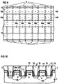
- an insulation region which defines a cell field for the memory cell arrangement (not shown) is first produced in a substrate 1 made of, for example, monocrystalline silicon on a main surface 2 of the substrate 1.
- the isolation area is formed, for example, by a LOCOS process or an STI (Shallow Trench Isolation) process.
- the substrate 1 is, for example, p-doped with a dopant concentration of 10 15 cm -3 .
- the depletion channels 3 are formed with the aid of a first channel implantation with arsenic with an energy of, for example, 40 keV and a dose of 4 ⁇ 10 13 cm -2 .
- the extent of the depletion channels 3 parallel to the main surface 2 is 2 F x 2 F, that is, for example 0.8 ⁇ m x 0.8 ⁇ m when using 0.4 ⁇ m technology (see FIG. 1).
- a trench mask 4 is formed by depositing an SiO 2 layer in a thickness of, for example, 100 nm to 200 nm using a TEOS method and then structuring the SiO 2 layer using photolithographic methods (see FIG. 2).
- strip-shaped trenches 5 are etched using the trench mask 4 as the etching mask.
- the trenches 5 have a depth of, for example, 0.5 ⁇ m.
- the width of the trenches 5 is F, for example 0.4 ⁇ m, the distance between adjacent trenches 5 is also F, for example 0.4 ⁇ m.
- the length of the trenches 5 depends on the size of the memory cell arrangement and is, for example, 130 ⁇ m.
- the width of the depletion channels 3 is set to the spacing of the trenches 5 during the etching of the trenches 5. thats why the adjustment of the trench mask 4 relative to the depletion channels 3 is not critical.
- a first resist mask 6 is then formed using photolithographic process steps (see FIG. 3, FIG. 4, FIG. 5).
- the first paint mask 6 has strip-shaped openings which run perpendicular to the trenches 5 (see supervision in FIG. 3).
- the width of the openings is F, for example 0.4 ⁇ m, the distance between adjacent openings is also F, for example 0.4 ⁇ m.
- insulation structures 7 are produced on the side walls of the trenches.
- the isolation structures 7 are formed, for example, by an angled implantation with boron ions. The angle during the ion implantation is chosen so that only the side walls lie within the implantation beam and the bottom of the trenches 5 is shaded.
- the implantation is carried out from two sides, so that insulation structures 7 are formed on both side walls.
- the implantation takes place, for example, with boron ions at an angle of 15 °, with an energy of, for example, 25 keV and a dose of 10 14 cm -2 .
- the insulation structures 7 can be formed by diffusion out of spacers which are suitable as a diffusion source.
- the spacers are produced, for example, from boron-doped glass by depositing a boron-doped glass layer and anisotropic etching back on the side walls of the trenches 5. They are then structured with the aid of a lacquer mask in such a way that they only remain on the areas of the side wall where insulation structures 7 are to be formed.
- the resist mask used for structuring has strip-shaped openings which are complementary to the openings of the first resist mask 6.
- the insulation structures 7 can be formed in the form of insulating spacers.
- the spacers are structured in such a way that the insulation structures 7 are created.
- a second paint mask (not shown) is formed.
- a second channel implantation is carried out, in which a higher threshold voltage is generated in the side walls of the trenches by an inclined implantation of, for example, boron with an energy of 25 keV and a dose of, for example, 5 ⁇ 10 12 cm -2 (not shown) .
- the vertical MOS transistors are programmed in this process step.
- a gate dielectric 8, for example made of thermal SiO 2 in a layer thickness of, for example, 5 to 10 nm is subsequently formed on the side walls of the trenches 5 (see FIG. 6).
- a doped polysilicon layer with conformal edge covering and a thickness of, for example, 50 nm is formed over the entire surface.
- the doped polysilicon layer is n + doped, for example. It is generated by in situ-doped deposition or by undoped deposition and subsequent doping by diffusion or implantation.
- doped polysilicon spacers 9 are formed on the side walls of the trenches. This etching is carried out selectively for the gate dielectric.
- the doped polysilicon spacers 9 run on the side walls of the trenches 5 over the entire length of the trenches 5 (see FIG. 6 and FIG. 7).
- the metal silicide layer is formed, for example, by reaction with tungsten. This takes advantage of the fact that the tungsten silicide only forms on the polysilicon, not but on the trench floors and bars covered with gate dielectric.
- a third channel implantation is performed using a third resist mask (not shown). 5 depletion channels 10 are formed at the bottom of the trenches. The third paint mask is then removed again.
- the trench mask 4 is then removed by wet chemical etching, for example using hydrofluoric acid.
- portions of the gate dielectric 8 located at the bottom of the trenches 5 are also removed.
- Isolating spacers 11, which completely cover the doped polysilicon spacers 9, are formed by full-surface deposition, for example in a TEOS process and subsequent anisotropic etching back of an SiO 2 layer (see FIG. 7 and FIG. 8).
- the SiO 2 layer is deposited in a layer thickness of, for example, 30 to 80 nm.
- a further gate dielectric 12 is subsequently formed, for example from thermal SiO 2 .
- the further gate dielectric 12 is arranged on the bottom of the trenches 5 and on the main surface 2 between adjacent trenches 5. It has a layer thickness of, for example, 5 to 10 nm.
- a polysilicon layer and an SiO 2 layer are then deposited.
- the polysilicon layer is deposited, for example, in situ doped or deposited undoped and then doped by implantation or diffusion, for example from the gas phase.
- the SiO 2 layer is deposited, for example, in a TEOS process.
- a hard mask (not shown) is formed from the SiO 2 layer using photolithographic processes.
- the doped polysilicon layer is structured using the hard mask as an etching mask.
- First word lines 13 running transversely to the trenches 5 are produced (see FIG. 7). The structuring of the first word lines 13 takes place in a highly selective manner with respect to the further gate dielectric 12 this structuring using a dry etching process with HBr and Cl 2 .
- the first word lines 13 are arranged such that they each run above the insulation structures 7. An adjustment with respect to the insulation structures 7 is therefore necessary to produce the first word lines 13.
- An arsenic implantation is subsequently carried out at an energy of, for example, 80 keV and a dose of, for example, 5 ⁇ 10 15 cm -2 , in the case of source / drain regions 14a on the main surface 2 and source / drain regions 14b on the bottom the trenches 5 are formed.
- the source / drain regions 14a, 14b each have a depth of 100 nm (see FIG. 8). After the formation of the source / drain regions 14a, 14b, the hard mask is removed.
- Two source / drain regions 14a each on the main surface 2 and the part of the p-doped substrate 1 adjoining the main surface 2 with or without depletion channel 3, as well as the further gate dielectric 12 arranged thereover and the part of the respective first word line arranged above it 13 each form a planar MOS transistor.
- the doped polysilicon spacers 9 form second word lines, via which the vertical MOS transistors are driven.
- the doped polysilicon spacers 9 are insulated from the first word lines 13 by the insulating spacers 11.
- FIG. 9 shows a top view of the sections shown in FIGS. 7 and 8.
- the position of the doped polysilicon spacers 9 was entered into this supervision as dashed lines.
- the first word lines 13 and the doped polysilicon spacers 9, which form the second word lines, run perpendicular to one another.
- the source / drain regions 14a, 14b have dimensions of F x F parallel to the main surface 2. They are arranged directly next to each other (see Figure 9). The distance between adjacent source / drain regions 14a, 14b parallel to the trenches 5 is also F.
- Each source / drain region 14a, 14b belongs to two adjacent planar MOS transistors.
- the vertical MOS transistors are implemented in the side walls of the trenches 5 and do not require any area parallel to the main area 2. Therefore, the area requirement for two memory cells, which comprise a planar MOS transistor and a vertical MOS transistor, is 2 F 2 . The average space requirement per memory cell is therefore F 2 .
- an intermediate oxide layer 15 is produced over the entire surface (see FIG. 10).
- the intermediate oxide layer 15 is formed in a layer thickness of, for example, 1600 nm.
- Contact holes are opened in the intermediate oxide layer 15 to source / drain regions 14b located at the bottom of the trenches 5.
- the side walls of the contact holes are provided with insulating spacers 16.
- the insulating spacers 16 are formed, for example, by depositing an SiO 2 layer in a TEOS process in a layer thickness of, for example, 30 to 80 nm and anisotropic etching back of the SiO 2 layer.
- the spacers 16 may cover parts of the source / drain regions 14a or the word lines 13 located on the main surface 2 as a result of adjustment errors.
- the contact holes are finally filled with metal fillings 17.
- a metal layer is applied by sputtering or vapor deposition and structured using photolithographic process steps and an etching step.
- the metal fillings 17 are formed, for example, from aluminum or tungsten.
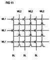
- FIG. 11 shows a circuit diagram for a memory cell array with 3 ⁇ 3 memory cell pairs.
- the individual memory cells are arranged in a NAND configuration.
- WL1 denotes the first word lines 13, which each connect gate electrodes of planar MOS transistors to one another.
- WL2 denotes the second word lines which are formed by the doped polysilicon spacers 9 and which each connect gate electrodes of vertical MOS transistors to one another.
- BL denotes the bit lines which are implemented by the planar MOS transistors which are respectively connected in series and are arranged on the main surface 2 and on the bottom of the trenches 5.
- the planar MOS transistors are evaluated via the bit lines BL and the respective first word lines WL1.
- the vertical MOS transistors are each evaluated between an adjacent bit line BL of planar MOS transistors which are arranged on the main surface 2 and the source / drain region 14b arranged at the bottom of the trench 5, which via the metal filling 17 has a reference potential is placed.
- the programming of the memory cell arrangement takes place during the production of the memory cell arrangement through the first channel implantation, the second channel implantation and the third channel implantation.
- the information stored in the process is transferred via the arrangement of the openings in the lacquer masks used in the channel implantations.
- the second channel implantation for programming the vertical MOS transistors can alternatively take place after the production of the first word lines 13.
- the second resist mask is generated above the hard mask that is used to structure the first word lines 13.
- the openings overlap the hard mask, so that the adjustment of the second paint mask parallel to the course of the trenches is not critical.
- the depletion channels in the side walls of the trenches are formed by oblique implantation of boron.
- the energy during the ion implantation is adjusted so that the boron ions pass through the doped polysilicon spacer 9 and the gate dielectric 8 into the side wall of the trenches 5.
- the implantation takes place, for example, with an energy of 50 keV.
- Different threshold voltages of the MOS transistors can also be realized during production by forming gate dielectrics of different thicknesses in the planar and / or vertical MOS transistors.
- a material with adhesion points is used as the gate dielectric 8 and as the further gate dielectric 12.
- the gate dielectric 8 and the further gate dielectric 12 are formed, for example, from a dielectric multiple layer, in which at least one layer is provided, which has an increased charge carrier capture cross section in comparison with at least one further layer in the multiple layer.
- the dielectric multilayer preferably comprises an SiO 2 layer, an Si 3 N 4 layer and an SiO 2 layer (so-called ONO).
- the layer thicknesses in the multilayer are dimensioned such that the multilayer corresponds in terms of the gate capacitance to a layer made of thermal SiO with a thickness of, for example, 10 nm.
- layer thicknesses of 4 nm each and a layer thickness of 4 nm is required for the Si 3 N 4 layer.
- the memory cell arrangement is programmed after its production by injecting charge carriers, especially electrons, into the gate dielectric 8 or the further gate dielectric 12.
- the charge carriers can be made by Fowler -Nordheim tunnels or hot electron injection.
- the first channel implantation, the second channel implantation and the third channel implantation as well as the lacquer masks used in this case are omitted.
- enhancement transistors for the planar MOS transistors and the vertical MOS transistors.
- the different threshold voltages are set to, for example, 0.5 volts and 1.5 volts.
Abstract
Description
Zur Abspeicherung großer Datenmengen, zum Beispiel für DV-Anwendungen oder zur digitalen Abspeicherung von Musik oder Bildern, werden derzeit hauptsächlich Speichersysteme mit mechanisch bewegten Teilen wie zum Beispiel Festplattenspeicher, Floppy-Disks oder Compact Disks verwendet. Die bewegten Teile sind mechanischem Verschleiß unterworfen. Ferner benötigen sie vergleichsweise viel Volumen und erlauben nur einen langsamen Datenzugriff. Da sie darüber hinaus erschütterungs- und lageempfindlich sind und einen vergleichsweise hohen Energieverbrauch zu ihrem Betrieb haben, sind diese Speichersysteme in mobilen Systemen nur begrenzt einsetzbar.For the storage of large amounts of data, for example for DV applications or for the digital storage of music or images, storage systems with mechanically moving parts, such as hard disk storage, floppy disks or compact disks, are currently mainly used. The moving parts are subject to mechanical wear. Furthermore, they require a comparatively large volume and only allow slow data access. Since they are also sensitive to vibrations and situations and have a comparatively high energy consumption for their operation, these storage systems can only be used to a limited extent in mobile systems.
Zur Speicherung kleinerer Datenmengen sind Festwertspeicher auf Halbleiterbasis bekannt. Vielfach werden diese als planare integrierte Siliziumschaltung realisiert, in der als Speicherzellen MOS-Transistoren verwendet werden. Die Transistoren werden über die Gateelektrode, die mit der Wortleitung verbunden ist, ausgewählt. Der Eingang des MOS-Transistors ist mit einer Referenzleitung verbunden, der Ausgang mit einer Bitleitung. Beim Lesevorgang wird bewertet, ob ein Strom durch den Transistor fließt oder nicht. Entsprechend werden die logischen Werte Null und Eins zugeordnet. Technisch wird die Speicherung von Null und Eins dadurch bewirkt, daß in Speicherzellen, in denen der dem Zustand ![]()
![]()
Diese Speicher auf Halbleiterbasis erlauben einen wahlfreien Zugriff auf die gespeicherte Information. Die zum Lesen der Information erforderliche elektrische Leistung ist deutlich kleiner als bei den erwähnten Speichersystemen mit mechanisch bewegten Teilen. Da keine bewegten Teile erforderlich sind, entfällt hier auch der mechanische Verschleiß und die Empfindlichkeit gegenüber Erschütterungen. Speicher auf Halbleiterbasis sind daher auch für mobile Systeme einsetzbar.These semiconductor-based memories allow random access to the stored information. The one for reading the The electrical power required for information is significantly smaller than in the aforementioned storage systems with mechanically moving parts. Since no moving parts are required, mechanical wear and sensitivity to vibrations are also eliminated. Semiconductor-based memories can therefore also be used for mobile systems.
Die beschriebenen Siliziumspeicher weisen einen planaren Aufbau auf. Damit wird pro Speicherzelle ein minimaler Flächenbedarf erforderlich, der im günstigsten Fall bei 4 F2 liegt, wobei F die in der jeweiligen Technologie kleinste herstellbare Strukturgröße ist.The silicon memories described have a planar structure. This means that a minimum space requirement is required per memory cell, which in the best case is 4 F 2 , where F is the smallest structure size that can be produced in the respective technology.
Aus US-PS 4 954 854 ist bekannt, in einem Festwertspeicher vertikale MOS-Transistoren zu verwenden. Dazu wird die Oberfläche eines Siliziumsubstrats mit Gräben versehen, an die am Boden ein Sourcegebiet angrenzt, an die an der Substratoberfläche ein Draingebiet angrenzt und entlang deren Flanken ein Kanalgebiet angeordnet ist. Die Oberfläche des Grabens wird mit einem Gatedielektrikum versehen und der Graben mit einer Gateelektrode aufgefüllt. Null und Eins werden in dieser Anordnung dadurch unterschieden, daß für einen der logischen Werte kein Graben geätzt und kein Transistor hergestellt wird.From US Pat. No. 4,954,854 it is known to use vertical MOS transistors in a read-only memory. For this purpose, the surface of a silicon substrate is provided with trenches, to which a source region adjoins at the bottom, to which a drain region adjoins the substrate surface and a channel region is arranged along the flanks thereof. The surface of the trench is provided with a gate dielectric and the trench is filled with a gate electrode. Zero and one are distinguished in this arrangement in that no trench is etched and no transistor is produced for one of the logic values.
Aus DE 42 14 923 A1 ist eine Festwertspeicherzellenanordnung bekannt, deren Speicherzellen MOS-Transistoren umfassen. Diese MOS-Transistoren sind entlang Gräben so angeordnet, daß ein Sourcegebiet an den Boden des Grabens angrenzt, ein Draingebiet an die Oberfläche des Substrats angrenzt und ein Kanalgebiet sowohl vertikal zur Oberfläche des Substrats als auch parallel zur Oberfläche des Substrats an Flanke und Boden des Grabens angrenzt. Die Oberfläche des Kanalgebietes ist mit einem Gatedielektrikum versehen. Die Gateelektrode ist als Flankenbedeckung (Spacer) ausgebildet. Die logischen Werte Null und Eins werden durch unterschiedliche Einsatzspannungen, die durch Kanalimplantation bewirkt werden, unterschieden. Bei der Kanalimplantation treffen die implantierenden Ionen unter einem solchen Winkel auf die Oberfläche des jeweiligen Grabens, daß durch Abschattungseffekte der gegenüberliegenden Flanke gezielt nur entlang einer Flanke implantiert wird.A read-only memory cell arrangement is known from DE 42 14 923 A1, the memory cells of which comprise MOS transistors. These MOS transistors are arranged along trenches such that a source region adjoins the bottom of the trench, a drain region adjoins the surface of the substrate and a channel region both vertically to the surface of the substrate and parallel to the surface of the substrate at the flank and bottom of the trench adjacent. The surface of the channel area is provided with a gate dielectric. The gate electrode is designed as a flank covering (spacer). The logical values zero and one are distinguished by different threshold voltages that are caused by channel implantation. In the case of channel implantation, the implanting ions hit the surface of the respective trench at such an angle that shadowing effects on the opposite flank are used to implant only along one flank.
Der Erfindung liegt das Problem zugrunde, eine Speicherzellenanordnung auf Halbleiterbasis anzugeben, bei der eine erhöhte Speicherdichte erzielt wird, so daß sie als Lesespeicher für große Datenmengen geeignet ist, und die mit wenigen Herstellungsschritten und hoher Ausbeute herstellbar ist. Desweiteren soll ein Verfahren zur Herstellung einer solchen Speicherzellenanordnung angegeben werden.The invention is based on the problem of specifying a memory cell arrangement based on semiconductors, in which an increased storage density is achieved, so that it is suitable as a read memory for large amounts of data, and which can be produced with few production steps and high yield. Furthermore, a method for producing such a memory cell arrangement is to be specified.
Dieses Problem wird erfindungsgemäß gelöst durch eine Speicherzellenanordnung gemäß Anspruch 1 sowie durch ein Verfahren zu deren Herstellung gemäß Anspruch 11. Weitere Ausgestaltungen der Erfindung ergeben sich aus den Unteransprüchen.This problem is solved according to the invention by a memory cell arrangement according to
Die erfindungsgemäße Speicherzellenanordnung ist in einem Halbleitersubstrat realisiert. Als Halbleitersubstrat wird vorzugsweise ein Substrat verwendet, das mindestens im Bereich einer Hauptfläche monokristallines Silizium aufweist. Als Halbleitersubstrat ist sowohl eine monokristalline Siliziumscheibe als auch ein SOI-Substrat geeignet.The memory cell arrangement according to the invention is implemented in a semiconductor substrate. A substrate which has monocrystalline silicon at least in the region of a main surface is preferably used as the semiconductor substrate. Both a monocrystalline silicon wafer and an SOI substrate are suitable as the semiconductor substrate.
Die Speicherzellenanordnung weist eine Vielzahl von Speicherzellen auf, die jeweils mindestens einen MOS-Transistor umfassen. Dabei umfassen erste Speicherzellen planare MOS-Transistoren, die in parallel verlaufenden Zeilen angeordnet sind. In der Hauptfläche des Halbleitersubstrats sind im wesentlichen parallel verlaufende, streifenförmige Gräben vorgesehen, die parallel zu den Zeilen verlaufen. Die Zeilen sind abwechselnd am Boden der Gräben und an der Hauptfläche zwischen benachbarten Gräben angeordnet.The memory cell arrangement has a multiplicity of memory cells, each of which comprises at least one MOS transistor. First memory cells include planar MOS transistors, which are arranged in parallel lines. In the main surface of the semiconductor substrate, essentially parallel, strip-shaped trenches are provided, which run parallel to the rows. The rows are arranged alternately on the bottom of the trenches and on the main area between adjacent trenches.
Zweite Speicherzellen umfassen zur Hauptfläche vertikale MOS-Transistoren, die jeweils an den Seitenwänden der Gräben realisiert sind.Second memory cells include vertical MOS transistors on the main surface, which are each implemented on the side walls of the trenches.
Die ersten Speicherzellen und die zweiten Speicherzellen unterscheiden sich bezüglich der technologischen Ausführung des MOS-Transistors. Bezüglich der Speichermöglichkeiten sind die ersten Speicherzellen und die zweiten Speicherzellen jedoch gleichwertig.The first memory cells and the second memory cells differ with regard to the technological design of the MOS transistor. With regard to the storage options, however, the first memory cells and the second memory cells are equivalent.
Es liegt im Rahmen der Erfindung, die Speicherzellenanordnung bei der Herstellung der Speicherzellenanordnung dadurch zu programmieren, daß die MOS-Transistoren mit unterschiedlichen Schwellenspannungen hergestellt werden. Dieses erfolgt vorzugsweise durch maskierte Kanalimplantation, bei der die Dotierung im Kanalbereich der MOS-Transistoren gezielt verändert wird.It is within the scope of the invention to program the memory cell arrangement in the production of the memory cell arrangement by producing the MOS transistors with different threshold voltages. This is preferably done by masked channel implantation, in which the doping in the channel region of the MOS transistors is specifically changed.
Alternativ werden unterschiedliche Schwellenspannungen der MOS-Transistoren dadurch realisiert, daß die MOS-Transistoren, je nach eingespeicherter Information, unterschiedlich dicke Gatedielektrika aufweisen. Dabei wird ausgenutzt, daß bei einem Unterschied der Dicken der Gatedielektrika um einen Faktor von 10 oder mehr sich die Einsatzspannungen der MOS-Transistoren so deutlich unterscheiden, daß bei Anlegen eines Auswahlsignales mit einem Pegel zwischen beiden Einsatzspannungen der eine MOS-Transistor leitet und der mit dem dickeren Gatedielektrikum nicht leitet.Alternatively, different threshold voltages of the MOS transistors are realized in that the MOS transistors, depending on the information stored, have gate dielectrics of different thicknesses. This takes advantage of the fact that if the thickness of the gate dielectrics differs by a factor of 10 or more, the threshold voltages of the MOS transistors differ so clearly that when a selection signal with a level between the two threshold voltages is applied, the one MOS transistor conducts and the one with does not conduct the thicker gate dielectric.
Soll die Speicherzellenanordnung für Mehrwertlogik eingesetzt werden, so weisen die MOS-Transistoren je nach eingespeicherter Information mehr als zwei unterschiedliche Schwellenspannungen auf.If the memory cell arrangement is to be used for value-added logic, the MOS transistors have more than two different threshold voltages, depending on the information stored.
Es liegt im Rahmen der Erfindung, für die MOS-Transistoren ein Gatedielektrikum aus einem Material mit Haftstellen vorzusehen. Haftstellen, englisch traps, haben die Eigenschaft, Ladungsträger, speziell Elektronen, einzufangen. Zur elektrischen Programmierung werden die MOS-Transistoren so beschaltet, daß der zu speichernden Information entsprechende Ladungsträger in das Gatedielektrikum gelangen und von den Haftstellen festgehalten werden.It is within the scope of the invention to provide a gate dielectric made of a material with adhesion points for the MOS transistors. Detention areas, English traps, have the property Capture charge carriers, especially electrons. For electrical programming, the MOS transistors are wired in such a way that the charge carriers corresponding to the information to be stored enter the gate dielectric and are held in place by the traps.
Die Programmierung dieser Speicherzellenanordnung erfolgt nach der Herstellung durch Injektion von Elektronen. Dieses kann sowohl durch Fowler-Nordheim-Tunneln als auch durch Hot-Electron-Injection erfolgen. Zur Abspeicherung von Daten in digitaler Form werden die MOS-Transistoren so programmiert, daß sie zwei unterschiedliche Schwellenspannungen aufweisen. Soll die Speicherzellenanordnung für Mehrwertlogik eingesetzt werden, so wird das Gatedielektrikum durch entsprechende Spannungs- und Zeitbedingungen bei der Programmierung so mit unterschiedlichen Ladungsmengen beaufschlagt, daß die MOS-Transistoren je nach eingespeicherter Information mehr als zwei unterschiedliche Schwellenspannungen aufweisen.This memory cell arrangement is programmed after production by injection of electrons. This can be done by Fowler-Nordheim tunnels as well as by hot electron injection. To store data in digital form, the MOS transistors are programmed so that they have two different threshold voltages. If the memory cell arrangement is to be used for value-added logic, then the gate dielectric is subjected to different charge quantities by appropriate voltage and time conditions during programming in such a way that the MOS transistors have more than two different threshold voltages, depending on the information stored.
Das Gatedielektrikum ist gemäß einer Ausführungsform der Erfindung als Mehrfachschicht ausgebildet, in der mindestens eine Schicht vorgesehen ist, die im Vergleich mit mindestens einer weiteren Schicht in der Mehrfachschicht einen erhöhten Ladungsträgereinfangquerschnitt aufweist. Die Haftstellen sind an der Grenzfläche zwischen beiden Schichten lokalisiert. Vorzugsweise umfaßt die dielektrische Mehrfachschicht eine SiO2-Schicht, eine Si3N4-Schicht und eine SiO2-Schicht (sogenanntes ONO). Alternativ kann das Gatedielektrikum als Mehrfachschicht aus anderen Materialien, wobei die Schicht mit dem erhöhten Ladungsträgereinfangquerschnitt zum Beispiel aus Si3N4, Ta2O5, Al2O3 oder aus TiO2 besteht und die benachbarte Schicht aus SiO2, Si3N4 oder Al2O3. Ferner kann die Mehrfachschicht mehr oder weniger als zwei Schichten umfassen.According to one embodiment of the invention, the gate dielectric is designed as a multiple layer, in which at least one layer is provided which has an increased charge carrier cross-section in comparison with at least one further layer in the multiple layer. The traps are located at the interface between the two layers. The dielectric multilayer preferably comprises an SiO 2 layer, an Si 3 N 4 layer and an SiO 2 layer (so-called ONO). Alternatively, the gate dielectric can be a multilayer made of other materials, the layer with the increased charge carrier capture cross section consisting, for example, of Si 3 N 4 , Ta 2 O 5 , Al 2 O 3 or TiO 2 and the adjacent layer of SiO 2 , Si 3 N 4 or Al 2 O 3 . Furthermore, the multilayer can comprise more or less than two layers.
Alternativ kann das Gatedielektrikum eine dielektrische Schicht, zum Beispiel aus SiO2, umfassen, in die Fremdatome, zum Beispiel W, Pt, Cr, Ni, Pd, Si oder Ir eingelagert sind. Die eingelagerten Fremdatome können durch Implantation, durch Zugabe bei einer Oxidation oder durch Diffusion eingebracht werden. Die eingelagerten Fremdatome bilden in diesem Fall die Haftstellen.Alternatively, the gate dielectric can comprise a dielectric layer, for example made of SiO 2 , into which foreign atoms for example, W, Pt, Cr, Ni, Pd, Si or Ir are embedded. The embedded foreign atoms can be introduced by implantation, by addition during oxidation or by diffusion. In this case, the embedded foreign atoms form the detention points.
Vorzugsweise sind in der erfindungsgemäßen Speicherzellenanordnung in einer Zeile angeordnete planare MOS-Transistoren in Reihe verschaltet. Miteinander verbundene Source/Drain-Gebiete von entlang einer Zeile benachbarten planaren MOS-Transistoren sind dabei als zusammenhängendes, dotiertes Gebiet ausgebildet. Die beiden Source/Drain-Gebiete jedes der vertikalen MOS-Transistoren sind jeweils mit einem der Source/Drain-Gebiete eines der planaren MOS-Transistoren an der Hauptfläche des Substrats und mit einem der Source/Drain-Gebiete der planaren MOS-Transistoren am Boden der Gräben als zusammenhängendes dotiertes Gebiet ausgebildet.In the memory cell arrangement according to the invention, planar MOS transistors arranged in one row are preferably connected in series. Interconnected source / drain regions of planar MOS transistors adjacent along a row are formed as a coherent, doped region. The two source / drain regions of each of the vertical MOS transistors are each with one of the source / drain regions of one of the planar MOS transistors on the main surface of the substrate and with one of the source / drain regions of the planar MOS transistors on the bottom the trenches are formed as a continuous doped area.
Werden in dieser Ausführungsform die Gräben mit einer Breite F und einem Abstand F gebildet, wobei F die in der jeweiligen Technologie kleinste herstellbare Strukturgröße ist, und wird die Abmessung der Source/Drain-Gebiete und des Kanalgebiets der planaren MOS-Transistoren in Richtung der Zeilen jeweils entsprechend F gewählt, so sind auf einer Fläche von 2 F2 eine erste Speicherzelle mit einem planaren MOS-Transistor und eine zweite Speicherzelle mit einem vertikalen MOS-Transistor angeordnet. Der mittlere Flächenbedarf pro Speicherzelle beträgt daher 1 F2. Diese erhöhte Packungsdichte wird dadurch erzielt, daß die vertikalen MOS-Transistoren jeweils an den Seitenwänden der Gräben angeordnet sind und keine zusätzliche Fläche in der Projektion auf die Hauptfläche benötigen. Die entlang benachbarter Zeilen angeordneten planaren MOS-Transistoren sind durch das Kanalgebiet der an der jeweiligen Seitenwand angeordneten vertikalen MOS-Transistoren gegeneinander isoliert.In this embodiment, the trenches are formed with a width F and a distance F, where F is the smallest structure size that can be produced in the respective technology, and the dimension of the source / drain regions and the channel region of the planar MOS transistors in the direction of the rows chosen in accordance with F, a first memory cell with a planar MOS transistor and a second memory cell with a vertical MOS transistor are arranged on an area of 2 F 2 . The average space requirement per memory cell is therefore 1 F 2 . This increased packing density is achieved in that the vertical MOS transistors are arranged on the side walls of the trenches and do not require any additional area in the projection onto the main area. The planar MOS transistors arranged along adjacent rows are insulated from one another by the channel region of the vertical MOS transistors arranged on the respective side wall.
Gemäß einer Ausführungsform der Erfindung sind eine Vielzahl erster Wortleitungen vorgesehen, die quer zu den Gräben verlaufen und die mit Gateelektroden von entlang unterschiedlichen Zeilen angeordneten planaren MOS-Transistoren verbunden sind. Ferner ist eine Vielzahl zweiter Wortleitungen vorgesehen, die jeweils paarweise in einem der Gräben angeordnet sind. Dabei sind die Gateelektroden von entlang einer der Seitenwände der Gräben angeordneten verikalen MOS-Transistoren mit einer der zweiten Wortleitungen verbunden. Zwischen je zwei benachbarten vertikalen MOS-Transistoren, die an derselben Seitenwand angeordnet sind, ist eine Isolationsstruktur vorgesehen, die die Ausbildung leitender Kanäle zwischen benachbarten MOS-Transistoren unterdrückt.According to one embodiment of the invention, a plurality of first word lines are provided, which run transversely to the trenches and which are connected to gate electrodes of planar MOS transistors arranged along different lines. Furthermore, a plurality of second word lines are provided, which are each arranged in pairs in one of the trenches. The gate electrodes of vertical MOS transistors arranged along one of the side walls of the trenches are connected to one of the second word lines. An insulation structure is provided between each two adjacent vertical MOS transistors, which are arranged on the same side wall, which suppresses the formation of conductive channels between adjacent MOS transistors.
Die Isolationsstrukturen sind vorzugsweise als dotiertes Gebiet in der jeweiligen Seitenwand ausgebildet. Die Dotierstoffkonzentration in dem dotierten Gebiet ist dabei so hoch, daß bei Anliegen einer Spannung an der betreffenden Wortleitung der zwischen benachbarten MOS-Transistoren gebildete, parasitäre MOS-Transistor nicht leitet. Alternativ können die Isolationsstrukturen auch als isolierende Spacer, zum Beispiel aus SiO2, gebildet werden.The insulation structures are preferably formed as a doped region in the respective side wall. The dopant concentration in the doped region is so high that the parasitic MOS transistor formed between adjacent MOS transistors does not conduct when a voltage is applied to the relevant word line. Alternatively, the insulation structures can also be formed as insulating spacers, for example made of SiO 2 .
Die Speicherzellenanordnung kann sowohl mit Enhancement-MOS-Transistoren als auch mit Depletion-MOS-Transistoren realisiert werden. Im Fall von Depletion-MOS-Transistoren werden jedoch im Hinblick auf eine wirksame Leckstromunterdrückung negative Ansteuerspannungen erforderlich. Bei Verwendung von Enhancement-MOS-Transistoren wird eine wirksame Leckstromunterdrückung auch bei Verwendung von positiven Ansteuerspannungen erzielt.The memory cell arrangement can be implemented both with enhancement MOS transistors and with depletion MOS transistors. In the case of depletion MOS transistors, however, negative drive voltages are required for effective leakage current suppression. When using enhancement MOS transistors, effective leakage current suppression is achieved even when using positive drive voltages.
Die Herstellung der erfindungsgemäßen Speicherzellenanordnung erfolgt vorzugsweise unter Einsatz selbstjustierender Prozeßschritte, so daß der Platzbedarf pro Speicherzelle reduziert wird.The memory cell arrangement according to the invention is preferably produced using self-adjusting process steps, so that the space requirement per memory cell is reduced.
Zur Herstellung der Speicherzellenanordnung werden in der Hauptfläche des Halbleitersubstrats streifenförmige, parallel verlaufende Gräben geätzt. Die vertikalen MOS-Transistoren werden in den Seitenwänden der Gräben, die planaren MOS-Transistoren am Boden der Gräben und zwischen benachbarten Gräben an der Hauptfläche gebildet.To produce the memory cell arrangement, stripe-shaped, parallel trenches are etched in the main surface of the semiconductor substrate. The vertical MOS transistors are formed in the side walls of the trenches, the planar MOS transistors on the bottom of the trenches and between adjacent trenches on the main surface.
Vorzugsweise werden quer zu den Gräben verlaufende erste Wortleitungen gebildet. Bei einer nachfolgenden Implantation zur Bildung von Source/Drain-Gebieten für die planaren MOS-Transistoren und für die vertikalen MOS-Transistoren wirken die ersten Wortleitungen als Maske.First word lines running transverse to the trenches are preferably formed. In a subsequent implantation to form source / drain regions for the planar MOS transistors and for the vertical MOS transistors, the first word lines act as a mask.
Vorzugsweise werden die zweiten Wortleitungen als Spacer aus zum Beispiel dotiertem Polysilizium an den Seitenwänden der Gräben gebildet. Zur Isolation zwischen den ersten Wortleitungen und den zweiten Wortleitungen wird die Oberfläche der zweiten Wortleitungen vor der Bildung der ersten Wortleitungen mit isolierendem Material bedeckt. Dieses erfolgt zum Beispiel durch thermische Oxidation der Oberfläche zum Beispiel bei der Bildung eines Gateoxids oder durch Bildung isolierender Spacer zum Beispiel aus SiO2. Die Verwendung isolierender Spacer zur Isolation zwischen den ersten Wortleitungen und den zweiten Wortleitungen hat den Vorteil, daß die isolierenden Spacer in größerer Dicke und unabhängig von anderen Prozeßparametern wie zum Beispiel der Gateoxiddicke herstellbar sind.The second word lines are preferably formed as spacers from, for example, doped polysilicon on the side walls of the trenches. For isolation between the first word lines and the second word lines, the surface of the second word lines is covered with insulating material before the first word lines are formed. This is done, for example, by thermal oxidation of the surface, for example when a gate oxide is formed, or by forming insulating spacers, for example from SiO 2 . The use of insulating spacers for insulation between the first word lines and the second word lines has the advantage that the insulating spacers can be produced with a greater thickness and independently of other process parameters such as, for example, the gate oxide thickness.
Im folgenden wird die Erfindung anhand eines Beispiels und der Figuren näher erläutert. Die Darstellungen in den Figuren sind nicht maßstabsgetreu.
Figur 1- zeigt ein Substrat nach einer ersten Kanalimplantation.
Figur 2- zeigt das Substrat nach der Ätzung streifenförmiger Gräben.
Figur 3- zeigt eine Aufsicht auf das Substrat nach Bildung einer ersten Maske und Erzeugung von Isolationsstrukturen in den Seitenwänden der Gräben.
Figur 4- zeigt den in
Figur 3 mit IV-IV bezeichneten Schnitt durch das Substrat. Figur 5- zeigt den in
Figur 3 mit V-V bezeichneten Schnitt durch das Substrat. Dieser Schnitt entspricht dem inFigur 2 dargestellten Schnitt. Figur 6- zeigt den in
Figur 4 gezeigten Schnitt durch das Substrat nach Bildung der Gatedielektrika und Gateelektroden für die vertikalen MOS-Transistoren. - Figur 7
- zeigt den in
Figur 5 dargestellten Schnitt durch das Substrat nach Bildung isolierender Spacer, die die Gateelektroden der vertikalen MOS-Transistoren bedecken, nach Bildung der Gatedielektrika für die planaren MOS-Transistoren und nach Bildung von quer zu den Gräben verlaufenden ersten Wortleitungen. Figur 8zeigt den Figur 6 entsprechenden Schnitt durch das Substrat nach Bildung von Source/Drain-Gebieten.Figur 9- zeigt eine Aufsicht auf das Substrat. Die in Figur 7 und Figur 8 dargestellten Schnitte sind in
Figur 9 mit VII-VII bzw. VIII-VIII eingetragen. Figur 10zeigt den Figur 8 entsprechenden Schnitt durch das Substrat nach Bildung von Bitleitungskontakten auf die am Boden der Gräben angeordneten Source/Drain-Gebiete.Figur 11- zeigt ein Schaltungsbild für eine Speicherzellenanordnung mit 3 x 3 Speicherzellenpaaren.
- Figure 1
- shows a substrate after a first channel implantation.
- Figure 2
- shows the substrate after the etching of strip-shaped trenches.
- Figure 3
- shows a plan view of the substrate after formation of a first mask and generation of isolation structures in the side walls of the trenches.
- Figure 4
- shows the section designated IV-IV in FIG. 3 through the substrate.
- Figure 5
- shows the section designated VV in FIG. 3 through the substrate. This section corresponds to the section shown in FIG. 2.
- Figure 6
- shows the section shown in Figure 4 through the substrate after formation of the gate dielectrics and gate electrodes for the vertical MOS transistors.
- Figure 7
- 5 shows the section through the substrate shown in FIG. 5 after the formation of insulating spacers which cover the gate electrodes of the vertical MOS transistors, after the formation of the gate dielectrics for the planar MOS transistors and after the formation of first word lines running transversely to the trenches.
- Figure 8
- shows the section corresponding to FIG. 6 through the substrate after formation of source / drain regions.
- Figure 9
- shows a top view of the substrate. The sections shown in Figure 7 and Figure 8 are entered in Figure 9 with VII-VII and VIII-VIII.
- Figure 10
- 8 shows a section through the substrate corresponding to FIG. 8 after the formation of bit line contacts on the source / drain regions arranged at the bottom of the trenches.
- Figure 11
- shows a circuit diagram for a memory cell arrangement with 3 x 3 memory cell pairs.
Zur Herstellung einer erfindungsgemäßen Speicherzellenanordnung wird in einem Substrat 1 aus zum Beispiel monokristallinem Silizium zunächst an einer Hauptfläche 2 des Substrats 1 ein Isolationsgebiet erzeugt, das ein Zellenfeld für die Speicherzellenanordnung definiert (nicht dargestellt). Das Isolationsgebiet wird zum Beispiel durch einen LOCOS-Prozeß oder einen STI (Shallow Trench Isolation)-Prozeß gebildet. Das Substrat 1 ist zum Beispiel p-dotiert mit einer Dotierstoffkonzentration von 1015 cm-3.To produce a memory cell arrangement according to the invention, an insulation region which defines a cell field for the memory cell arrangement (not shown) is first produced in a
Mit Hilfe eines photolithographischen Verfahrens werden dann Bereiche für Depletion-Kanäle von MOS-Transistoren definiert. Mit Hilfe einer ersten Kanalimplantation mit Arsen mit einer Energie von zum Beispiel 40 keV und einer Dosis von 4 x 1013 cm-2 werden die Depletion-Kanäle 3 gebildet. Die Ausdehnung der Depletion-Kanäle 3 parallel zur Hauptfläche 2 beträgt 2 F x 2 F, das heißt bei Verwendung einer 0,4 µm-Technologie zum Beispiel 0,8 µm x 0,8 µm (siehe Figur 1).Areas for depletion channels of MOS transistors are then defined with the aid of a photolithographic method. The
Durch Abscheidung einer SiO2-Schicht in einer Dicke von zum Beispiel 100 nm bis 200 nm mit Hilfe eines TEOS-Verfahrens und anschließende Strukturierung der SiO2-Schicht mit Hilfe photolithographischer Verfahren wird eine Grabenmaske 4 gebildet (siehe Figur 2).A
Durch anisotropes Ätzen zum Beispiel mit Cl2 werden unter Verwendung der Grabenmaske 4 als Ätzmaske streifenförmige Gräben 5 geätzt. Die Gräben 5 weisen eine Tiefe von zum Beispiel 0,5 µm auf. Die Weite der Gräben 5 beträgt F, zum Beispiel 0,4 µm, der Abstand benachbarter Gräben 5 beträgt ebenfalls F, zum Beispiel 0,4 µm. Die Länge der Gräben 5 richtet sich nach der Größe der Speicherzellenanordnung und beträgt zum Beispiel 130 µm.By anisotropic etching, for example with Cl 2 , strip-shaped
Die Breite der Depletion-Kanäle 3 wird bei der Ätzung der Gräben 5 auf den Abstand der Gräben 5 eingestellt. Daher ist die Justierung der Grabenmaske 4 relativ zu den Depletion-Kanälen 3 unkritisch.The width of the
Anschließend wird mit Hilfe photolithographischer Prozeßschritte eine erste Lackmaske 6 gebildet (siehe Figur 3, Figur 4, Figur 5). Die erste Lackmaske 6 weist streifenförmige Öffnungen auf, die senkrecht zu den Gräben 5 verlaufen (siehe Aufsicht in Figur 3). Die Weite der Öffnungen beträgt F, zum Beispiel 0,4 µm, der Abstand benachbarter Öffnungen beträgt ebenfalls F, zum Beispiel 0,4 µm. Im Bereich der Öffnungen der ersten Lackmaske 6 werden an den Seitenwänden der Gräben 5 Isolationsstrukturen 7 erzeugt. Die Isolationsstrukturen 7 werden zum Beispiel durch eine gewinkelte Implantation mit Borionen gebildet. Der Winkel bei der Ionenimplantation wird so gewählt, daß nur die Seitenwände innerhalb des Implantationsstrahles liegen und der Boden der Gräben 5 abgeschattet wird. Die Implantation wird dabei von zwei Seiten durchgeführt, so daß an beiden Seitenwänden Isolationsstrukturen 7 gebildet werden. Die Implantation erfolgt zum Beispiel mit Borionen unter einem Winkel von 15°, mit einer Energie von zum Beispiel 25 keV und einer Dosis von 1014 cm-2.A first resist
Alternativ können die Isolationsstrukturen 7 durch Ausdiffusion aus Spacern, die als Diffusionsquelle geeignet sind, gebildet werden. Die Spacer werden zum Beispiel aus bordotiertem Glas durch Abscheidung einer bordotierten Glasschicht und anisotropes Rückätzen an den Seitenwänden der Gräben 5 erzeugt. Anschließend werden sie mit Hilfe einer Lackmaske so strukturiert, daß sie nur an den Bereichen der Seitenwand stehenbleiben, an denen Isolationsstrukturen 7 gebildet werden sollen. Die zur Strukturierung verwendete Lackmaske weist streifenförmige Öffnungen auf, die komplementär zu den Öffnungen der ersten Lackmaske 6 sind.Alternatively, the insulation structures 7 can be formed by diffusion out of spacers which are suitable as a diffusion source. The spacers are produced, for example, from boron-doped glass by depositing a boron-doped glass layer and anisotropic etching back on the side walls of the
In einer weiteren Alternative können die Isolationsstrukturen 7 in Form von isolierenden Spacern gebildet werden. Dazu wird zum Beispiel in einem TEOS-Verfahren eine SiO2-Schicht in einer Schichtdicke von zum Beispiel 30 bis 80 nm abgeschieden und anisotrop zurückgeätzt. Mit Hilfe einer Lackmaske, die zu der ersten Lackmaske 6 komplementär ist, werden die Spacer so strukturiert, daß die Isolationsstrukturen 7 entstehen.In a further alternative, the insulation structures 7 can be formed in the form of insulating spacers. For this purpose, for example in a TEOS process, an SiO 2 layer in one Layer thickness of, for example, 30 to 80 nm deposited and etched back anisotropically. With the help of a resist mask, which is complementary to the first resist
Nach Entfernen der ersten Lackmaske 6 wird eine zweite Lackmaske (nicht dargestellt) gebildet. Es wird eine zweite Kanalimplantation durchgeführt, bei der durch eine geneigte Implantation von zum Beispiel Bor mit einer Energie von 25 keV und einer Dosis von zum Beispiel 5 x 10 12 cm-2 in den Seitenwänden der Gräben eine höhere Schwellenspannung erzeugt wird (nicht dargestellt). In diesem Prozeßschritt erfolgt die Programmierung der vertikalen MOS-Transistoren.After removing the
Nachfolgend wird an den Seitenwänden der Gräben 5 ein Gatedielektrikum 8 zum Beispiel aus thermischem SiO2 in einer Schichtdicke von zum Beispiel 5 bis 10 nm gebildet (siehe Figur 6).A
Es wird ganzflächig eine dotierte Polysiliziumschicht mit konformer Kantenbedeckung und einer Dicke von zum Beispiel 50 nm gebildet. Die dotierte Polysiliziumschicht ist zum Beispiel n+-dotiert. Sie wird durch insitu-dotierte Abscheidung oder durch undotierte Abscheidung und anschließende Dotierung durch Diffusion oder Implantation erzeugt. Durch anisotropes Rückätzen der dotierten Polysiliziumschicht werden an den Seitenwänden der Gräben 5 dotierte Polysiliziumspacer 9 gebildet. Diese Ätzung wird selektiv zum Gatedielektrikum durchgeführt. Die dotierten Polysiliziumspacer 9 verlaufen an den Seitenwänden der Gräben 5 über die gesamte Länge der Gräben 5 (siehe Figur 6 und Figur 7). Zur Reduktion des Schichtwiderstands der dotierten Polysiliziumspacer 9 ist es vorteilhaft, diese mit einer dünnen Metallsilizidschicht zu versehen. Die Metallsilizidschicht wird zum Beispiel durch Reaktion mit Wolfram gebildet. Dabei wird ausgenutzt, daß sich das Wolframsilizid nur auf dem Polysilizium ausbildet, nicht aber auf den von Gatedielektrikum bedeckten Grabenböden und Stegen.A doped polysilicon layer with conformal edge covering and a thickness of, for example, 50 nm is formed over the entire surface. The doped polysilicon layer is n + doped, for example. It is generated by in situ-doped deposition or by undoped deposition and subsequent doping by diffusion or implantation. By anisotropic etching back of the doped
Unter Verwendung einer dritten Lackmaske (nicht dargestellt) wird eine dritte Kanalimplantation durchgeführt. Dabei werden am Boden der Gräben 5 Depletion-Kanäle 10 gebildet. Anschließend wird die dritte Lackmaske wieder entfernt.A third channel implantation is performed using a third resist mask (not shown). 5
Anschließend wird die Grabenmaske 4 durch naßchemisches Ätzen zum Beispiel mit Flußsäure entfernt. Dabei werden auch am Boden der Gräben 5 befindliche Anteile des Gatedielektrikums 8 entfernt. Durch ganzflächige Abscheidung zum Beispiel in einem TEOS-Verfahren und anschließendes, anisotropes Rückätzen einer SiO2-Schicht werden isolierende Spacer 11 gebildet, die die dotierten Polysiliziumspacer 9 vollständig abdecken (siehe Figur 7 und Figur 8). Die SiO2-Schicht wird in einer Schichtdicke von zum Beispiel 30 bis 80 nm abgeschieden.The
Nachfolgend wird ein weiteres Gatedielektrikum 12 zum Beispiel aus thermischem SiO2 gebildet. Das weitere Gatedielektrikum 12 ist am Boden der Gräben 5 und an der Hauptfläche 2 zwischen benachbarten Gräben 5 angeordnet. Es weist eine Schichtdicke von zum Beispiel 5 bis 10 nm auf.A
Anschließend wird eine Polysiliziumschicht und eine SiO2-Schicht abgeschieden. Die Polysiliziumschicht wird zum Beispiel insitu dotiert abgeschieden oder undotiert abgeschieden und anschließend durch Implantation oder Diffusion zum Beispiel aus der Gasphase dotiert. Die SiO2-Schicht wird zum Beispiel in einem TEOS-Verfahren abgeschieden. Mit Hilfe photolithographischer Verfahren wird aus der SiO2-Schicht eine Hartmaske gebildet (nicht dargestellt). Unter Verwendung der Hartmaske als Ätzmaske wird die dotierte Polysiliziumschicht strukturiert. Dabei werden quer zu den Gräben 5 verlaufende erste Wortleitungen 13 erzeugt (siehe Figur 7). Die Strukturierung der ersten Wortleitungen 13 erfolgt hochselektiv gegen das weitere Gatedielektrikum 12. Vorzugsweise erfolgt diese Strukturierung unter Verwendung eines trockenen Ätzprozesses mit HBr und Cl2.A polysilicon layer and an SiO 2 layer are then deposited. The polysilicon layer is deposited, for example, in situ doped or deposited undoped and then doped by implantation or diffusion, for example from the gas phase. The SiO 2 layer is deposited, for example, in a TEOS process. A hard mask (not shown) is formed from the SiO 2 layer using photolithographic processes. The doped polysilicon layer is structured using the hard mask as an etching mask. First word lines 13 running transversely to the
Die ersten Wortleitungen 13 werden so angeordnet, daß sie jeweils oberhalb der Isolationsstrukturen 7 verlaufen. Zur Herstellung der ersten Wortleitungen 13 ist daher eine Justierung bezüglich der Isolationsstrukturen 7 erforderlich.The first word lines 13 are arranged such that they each run above the insulation structures 7. An adjustment with respect to the insulation structures 7 is therefore necessary to produce the first word lines 13.
Nachfolgend wird eine Implantation mit Arsen bei einer Energie von zum Beispiel 80 keV und einer Dosis von zum Beispiel 5 x 1015 cm-2 durchgeführt, bei der Source/Drain-Gebiete 14a an der Hauptfläche 2 und Source/Drain-Gebiete 14b am Boden der Gräben 5 gebildet werden. Die Source/Drain-Gebiete 14a, 14b weisen eine Tiefe von jeweils 100 nm auf (siehe Figur 8). Nach Bildung der Source-/Drain-Gebiete 14a, 14b wird die Hartmaske entfernt.An arsenic implantation is subsequently carried out at an energy of, for example, 80 keV and a dose of, for example, 5 × 10 15 cm -2 , in the case of source /
Je zwei Source/Drain-Gebiete 14a an der Hauptfläche 2 und der dazwischen an die Hauptfläche 2 angrenzende Teil des p-dotierten Substrats 1 mit oder ohne Depletion-Kanal 3 sowie das darüber angeordnete weitere Gatedielektrikum 12 und der darüber angeordnete Teil der jeweiligen ersten Wortleitung 13 bilden jeweils einen planaren MOS-Transistor. Ebenso bilden je zwei am Boden der Gräben 5 angeordnete Source/Drain-Gebiete 14b sowie der dazwischen an den Boden des Grabens 5 angeordnete Teil des p-dotierten Substrats 1 mit oder ohne Depletion-Kanal 10 sowie das darüber angeordnete weitere Gatedielektrikum 12 und der darüber angeordnete Teil der jeweiligen ersten Wortleitung 13 einen am Boden des Grabens 5 angeordneten, planaren MOS-Transistor. Je zwei an eine Seitenwand des Grabens 5 angrenzende Source/Drain-Gebiete 14a, 14b sowie der dazwischen an die Seitenwand angrenzende Teil des p-dotierten Substrats 1 mit oder ohne Depletion-Kanal bilden mit dem daran angrenzenden Teil des Gatedielektrikums 8 sowie der dotierten Polysiliziumspacer 9 einen vertikalen MOS-Transistor. Benachbarte planare MOS-Transistoren, die am Boden eines Grabens 5 und an der Hauptfläche angeordnet sind, sind durch das p-dotierte Substrat 1 gegeneinander isoliert. Die dotierten Polysiliziumspacer 9 bilden zweite Wortleitungen, über die die vertikalen MOS-Transistoren angesteuert werden. Die dotierten Polysiliziumspacer 9 sind gegen die ersten Wortleitungen 13 durch die isolierenden Spacer 11 isoliert.Two source /
In Figur 9 ist eine Aufsicht auf die in Figur 7 und 8 dargestellten Schnitte dargestellt. In diese Aufsicht wurden als gestrichelte Linien die Lage der dotierten Polysiliziumspacer 9 eingetragen. Die ersten Wortleitungen 13 und die dotierten Polysiliziumspacer 9, die die zweiten Wortleitungen bilden, verlaufen senkrecht zueinander.FIG. 9 shows a top view of the sections shown in FIGS. 7 and 8. The position of the doped
In dem Ausführungsbeispiel weisen die Source/Drain-Gebiete 14a, 14b parallel zur Hauptfläche 2 Abmessungen von F x F auf. Sie sind unmittelbar nebeneinander angeordnet (siehe Figur 9). Der Abstand zwischen benachbarten Source/Drain-Gebieten 14a, 14b parallel zu den Gräben 5 beträgt ebenfalls F. Jedes Source/Drain-Gebiet 14a, 14b gehört zwei benachbarten planaren MOS-Transistoren an. Die vertikalen MOS-Transistoren sind in den Seitenwänden der Gräben 5 realisiert und benötigen parallel zur Hauptfläche 2 keine Fläche. Daher beträgt der Flächenbedarf für zwei Speicherzellen, die einen planaren MOS-Transistor und einen vertikalen MOS-Transistor umfassen, 2 F2. Der mittlere Flächenbedarf pro Speicherzelle beträgt daher F2.In the exemplary embodiment, the source /
Zur Fertigstellung der Speicherzellenanordnung wird ganzflächig eine Zwischenoxidschicht 15 erzeugt (siehe Figur 10). Die Zwischenoxidschicht 15 wird in einer Schichtdicke von zum Beispiel 1600 nm gebildet. In der Zwischenoxidschicht 15 werden Kontaktlöcher zu am Boden der Gräben 5 befindlichen Source/Drain-Gebieten 14b geöffnet. Zur Vermeidung von Kurzschlüssen werden die Seitenwände der Kontaktlöcher mit isolierenden Spacern 16 versehen. Die isolierenden Spacer 16 werden zum Beispiel durch Abscheidung einer SiO2-Schicht in einem TEOS-Verfahren in einer Schichtdicke von zum Beispiel 30 bis 80 nm und anisotropes Rückätzen der SiO2-Schicht gebildet. Durch die Spacer 16 werden möglicherweise infolge von Justierfehlern freigeätzte Teile der an der Hauptfläche 2 befindlichen Source/Drain-Gebiete 14a oder der Wortleitungen 13 abgedeckt. Die Kontaktlöcher werden schließlich mit Metallfüllungen 17 aufgefüllt. Dazu wird zum Beispiel eine Metallschicht durch Sputtern oder Aufdampfen aufgebracht und mit Hilfe photolithographischer Prozeßschritte sowie einem Ätzschritt strukturiert. Die Metallfüllungen 17 werden zum Beispiel aus Aluminium oder Wolfram gebildet.To complete the memory cell arrangement, an
In Figur 11 ist ein Schaltbild für ein Speicherzellenfeld mit 3 x 3 Speicherzellenpaaren dargestellt. Die einzelnen Speicherzellen sind in einer NAND-Konfiguration angeordnet. Mit WL1 sind die ersten Wortleitungen 13 bezeichnet, die jeweils Gateelektroden von planaren MOS-Transistoren miteinander verbinden. Mit WL2 sind die zweiten Wortleitungen, die durch die dotierten Polysiliziumspacer 9 gebildet werden, bezeichnet, die jeweils Gateelektroden von vertikalen MOS-Transistoren miteinander verbinden. Mit BL sind die Bitleitungen bezeichnet, die durch die jeweils in Reihe verschalteten planaren MOS-Transistoren, die an der Hauptfläche 2 sowie am Boden der Gräben 5 angeordnet sind, realisiert sind. Die Bewertung der planaren MOS-Transistoren erfolgt über die Bitleitungen BL und die jeweiligen ersten Wortleitungen WL1. Die Bewertung der vertikalen MOS-Transistoren erfolgt jeweils zwischen einer benachbarten Bitleitung BL von planaren MOS-Transistoren, die an der Hauptfläche 2 angeordnet sind und dem am Boden des Grabens 5 angeordneten Source/Drain-Gebiet 14b, das über die Metallfüllung 17 auf ein Referenzpotential gelegt wird.FIG. 11 shows a circuit diagram for a memory cell array with 3 × 3 memory cell pairs. The individual memory cells are arranged in a NAND configuration. WL1 denotes the first word lines 13, which each connect gate electrodes of planar MOS transistors to one another. WL2 denotes the second word lines which are formed by the doped
In der beschriebenen Ausführungsform der Erfindung erfolgt die Programmierung der Speicherzellenanordnung bei der Herstellung der Speicherzellenanordnung durch die erste Kanalimplantation, die zweite Kanalimplantation und die dritte Kanalimplantation. Die dabei gespeicherte Information wird über die Anordnung der Öffnungen in den bei den Kanalimplantationen verwendeten Lackmasken eingebracht.In the described embodiment of the invention, the programming of the memory cell arrangement takes place during the production of the memory cell arrangement through the first channel implantation, the second channel implantation and the third channel implantation. The information stored in the process is transferred via the arrangement of the openings in the lacquer masks used in the channel implantations.
Die zweite Kanalimplantation zur Programmierung der vertikalen MOS-Transistoren kann alternativ nach der Herstellung der ersten Wortleitungen 13 erfolgen. Die zweite Lackmaske wird in diesem Fall oberhalb der Hartmaske, die zur Strukturierung der ersten Wortleitungen 13 verwendet wird, erzeugt. Die Öffnungen überlappen die Hartmaske, so daß die Justierung der zweiten Lackmaske parallel zum Verlauf der Gräben unkritisch ist. Die Depletion-Kanäle in den Seitenwänden der Gräben werden auch in diesem Fall durch schräge Implantation von Bor gebildet. Die Energie bei der Ionenimplantation wird dabei so eingestellt, daß die Borionen durch die dotierten Polysiliziumspacer 9 und das Gatedielektrikum 8 hindurch in die Seitenwand der Gräben 5 gelangen. Die Implantation erfolgt zum Beispiel mit einer Energie von 50 keV.The second channel implantation for programming the vertical MOS transistors can alternatively take place after the production of the first word lines 13. In this case, the second resist mask is generated above the hard mask that is used to structure the first word lines 13. The openings overlap the hard mask, so that the adjustment of the second paint mask parallel to the course of the trenches is not critical. In this case too, the depletion channels in the side walls of the trenches are formed by oblique implantation of boron. The energy during the ion implantation is adjusted so that the boron ions pass through the doped
Unterschiedliche Schwellenspannungen der MOS-Transistoren können bei der Herstellung auch durch Bildung unterschiedlich dicker Gatedielektrika der planaren und/oder vertikalen MOS-Transistoren realisiert werden.Different threshold voltages of the MOS transistors can also be realized during production by forming gate dielectrics of different thicknesses in the planar and / or vertical MOS transistors.
In einer weiteren Alternative wird als Gatedielektrikum 8 und als weiteres Gatedielektrikum 12 ein Material mit Haftstellen verwendet. Das Gatedielektrikum 8 und das weitere Gatedielektrikum 12 werden zum Beispiel aus einer dielektrischen Mehrfachschicht gebildet, in der mindestens eine Schicht vorgesehen ist, die im Vergleich mit mindestens einer weiteren Schicht in der Mehrfachschicht einen erhöhten Ladungsträgereinfangquerschnitt aufweist. Vorzugsweise umfaßt die dielektrische Mehrfachschicht eine SiO2-Schicht, eine Si3N4-Schicht und eine SiO2-Schicht (sogenanntes ONO). Die Schichtdicken in der Mehrfachschicht werden dabei so bemessen, daß die Mehrfachschicht bezüglich der Gatekapazität einer Schicht aus thermischem SiO mit einer Dicke von zum Beispiel 10 nm entspricht. Dazu sind für die SiO2-Schichten Schichtdicken von jeweils 4 nm und für die Si3N4-Schicht eine Schichtdicke von 4 nm erforderlich.In a further alternative, a material with adhesion points is used as the
Werden das Gatedielektrikum 8 und das weitere Gatedielektrikum 12 aus einem Material mit hoher Haftstellendichte gebildet, so erfolgt die Programmierung der Speicherzellenanordnung nach deren Herstellung durch Injektion von Ladungsträgern, speziell Elektronen, in das Gatedielektrikum 8 bzw. das weitere Gatedielektrikum 12. Die Ladungsträger können durch Fowler-Nordheim-Tunneln oder Hot-Electron-Injection eingebracht werden. In diesem Fall entfallen die erste Kanalimplantation, die zweite Kanalimplantation und die dritte Kanalimplantation sowie die dabei verwendeten Lackmasken.If the
Im Hinblick auf eine wirksame Leckstromunterdrückung zwischen den Speicherzellen ist es vorteilhaft, für die planaren MOS-Transistoren und die vertikalen MOS-Transistoren Enhancement-Transistoren zu verwenden. Zur Realisierung der Informationszustände ![]()
![]()
![]()
![]()
Claims (19)
bei der die Isolationsstrukturen (7) jeweils als dotiertes Gebiet in der jeweiligen Seitenwand ausgebildet sind.Memory cell arrangement according to claim 3,
in which the insulation structures (7) are each formed as a doped region in the respective side wall.
bei der die MOS-Transistoren je nach in der jeweiligen Speicherzelle eingespeicherter Information unterschiedliche Schwellenspannungen aufweisen.Memory cell arrangement according to one of claims 1 to 4,
in which the MOS transistors have different threshold voltages depending on the information stored in the respective memory cell.
bei der die MOS-Transistoren ein Gatedielektrikum (8, 12) aus einem Material mit Haftstellen aufweisen.Memory cell arrangement according to one of claims 1 to 4,
in which the MOS transistors have a gate dielectric (8, 12) made of a material with adhesion points.
bei der die MOS-Transistoren als Gatedielektrikum (8, 12) eine dielektrische Mehrfachschicht umfassen mit mindestens einer Schicht, die im Vergleich mit mindestens einer weiteren Schicht einen erhöhten Ladungsträgereinfangquerschnitt aufweist.Memory cell arrangement according to claim 6,
in which the MOS transistors as a gate dielectric (8, 12) comprise a dielectric multiple layer with at least one layer which has an increased charge carrier cross section in comparison with at least one further layer.
bei der die MOS-Transistoren als Gatedielektrikum (8, 12) eine dielektrische Schicht mit eingelagerten Fremdatomen umfassen, wobei die eingelagerten Fremdatome im Vergleich mit der dielektrischen Schicht einen erhöhten Ladungsträgereinfangquerschnitt aufweisen.Memory cell arrangement according to claim 6,
in which the MOS transistors as gate dielectric (8, 12) comprise a dielectric layer with embedded foreign atoms, the embedded foreign atoms having an increased charge carrier capture cross section compared to the dielectric layer.
bei dem zur Bildung der Isolationsstruktur (7) in der jeweiligen Seitenwand jeweils dotierte Gebiete gebildet werden.The method of claim 14
in which doped regions are formed in each side wall to form the insulation structure (7).
bei dem die MOS-Transistoren je nach eingespeicherter Information mit unterschiedlichen Schwellenspannungen hergestellt werden.Method according to one of claims 11 to 15,
in which the MOS transistors are manufactured with different threshold voltages depending on the information stored.
bei dem das Gatedielektrikum (8, 12) der MOS-Transistoren aus einem Material mit Haftstellen gebildet wird.Method according to one of claims 11 to 15,
in which the gate dielectric (8, 12) of the MOS transistors is formed from a material with traps.
bei dem das Gatedielektrikum (8, 12) als dielektrische Mehrfachschicht mit mindestens einer Schicht, die im Vergleich mit mindestens einer weiteren Schicht einen erhöhten Ladungsträgereinfangquerschnitt aufweist, gebildet wird.A method according to claim 17,
in which the gate dielectric (8, 12) is formed as a dielectric multilayer with at least one layer which has an increased charge carrier cross section in comparison with at least one further layer.
bei dem das Gatedielektrikum (8, 12) als dielektrische Schicht mit eingelagerten Fremdatomen gebildet wird, wobei die eingelagerten Fremdatome im Vergleich mit der dielektrischen Schicht einen erhöhten Ladungsträgereinfangquerschnitt aufweisen.A method according to claim 17,
in which the gate dielectric (8, 12) is formed as a dielectric layer with embedded foreign atoms, the embedded foreign atoms having an increased charge carrier capture cross section compared to the dielectric layer.
Applications Claiming Priority (2)
| Application Number | Priority Date | Filing Date | Title |
|---|---|---|---|
| DE19603810A DE19603810C1 (en) | 1996-02-02 | 1996-02-02 | Memory cell arrangement and method for its production |
| DE19603810 | 1996-02-02 |
Publications (3)
| Publication Number | Publication Date |
|---|---|
| EP0788165A2 true EP0788165A2 (en) | 1997-08-06 |
| EP0788165A3 EP0788165A3 (en) | 1997-12-10 |
| EP0788165B1 EP0788165B1 (en) | 2004-02-04 |
Family
ID=7784367
Family Applications (1)
| Application Number | Title | Priority Date | Filing Date |
|---|---|---|---|
| EP96119225A Expired - Lifetime EP0788165B1 (en) | 1996-02-02 | 1996-11-29 | Storage cell arrangement and method for making the same |
Country Status (6)
| Country | Link |
|---|---|
| US (2) | US5821591A (en) |
| EP (1) | EP0788165B1 (en) |
| JP (1) | JPH09213816A (en) |
| KR (1) | KR100400528B1 (en) |
| DE (2) | DE19603810C1 (en) |
| TW (1) | TW317033B (en) |
Cited By (21)
| Publication number | Priority date | Publication date | Assignee | Title |
|---|---|---|---|---|
| US7732816B2 (en) | 2001-06-18 | 2010-06-08 | Innovative Silicon Isi Sa | Semiconductor device |
| US7736959B2 (en) | 2003-07-22 | 2010-06-15 | Innovative Silicon Isi Sa | Integrated circuit device, and method of fabricating same |
| US8861247B2 (en) | 2009-04-27 | 2014-10-14 | Micron Technology, Inc. | Techniques for providing a direct injection semiconductor memory device |
| US8947965B2 (en) | 2009-07-27 | 2015-02-03 | Micron Technology Inc. | Techniques for providing a direct injection semiconductor memory device |
| US8964479B2 (en) | 2010-03-04 | 2015-02-24 | Micron Technology, Inc. | Techniques for sensing a semiconductor memory device |
| US8982633B2 (en) | 2009-05-22 | 2015-03-17 | Micron Technology, Inc. | Techniques for providing a direct injection semiconductor memory device |
| US9019788B2 (en) | 2008-01-24 | 2015-04-28 | Micron Technology, Inc. | Techniques for accessing memory cells |
| US9019759B2 (en) | 2010-03-15 | 2015-04-28 | Micron Technology, Inc. | Techniques for providing a semiconductor memory device |
| US9064730B2 (en) | 2009-03-04 | 2015-06-23 | Micron Technology, Inc. | Techniques for forming a contact to a buried diffusion layer in a semiconductor memory device |
| US9093311B2 (en) | 2009-03-31 | 2015-07-28 | Micron Technology, Inc. | Techniques for providing a semiconductor memory device |
| US9142264B2 (en) | 2010-05-06 | 2015-09-22 | Micron Technology, Inc. | Techniques for refreshing a semiconductor memory device |
| US9240496B2 (en) | 2009-04-30 | 2016-01-19 | Micron Technology, Inc. | Semiconductor device with floating gate and electrically floating body |
| US9257155B2 (en) | 2007-05-30 | 2016-02-09 | Micron Technology, Inc. | Integrated circuit having voltage generation circuitry for memory cell array, and method of operating and/or controlling same |
| US9263133B2 (en) | 2011-05-17 | 2016-02-16 | Micron Technology, Inc. | Techniques for providing a semiconductor memory device |
| US9276000B2 (en) | 2007-03-29 | 2016-03-01 | Micron Technology, Inc. | Manufacturing process for zero-capacitor random access memory circuits |
| US9331083B2 (en) | 2009-07-10 | 2016-05-03 | Micron Technology, Inc. | Techniques for providing a semiconductor memory device |
| US9553186B2 (en) | 2008-09-25 | 2017-01-24 | Micron Technology, Inc. | Recessed gate silicon-on-insulator floating body device with self-aligned lateral isolation |
| US9559216B2 (en) | 2011-06-06 | 2017-01-31 | Micron Technology, Inc. | Semiconductor memory device and method for biasing same |
| US9812179B2 (en) | 2009-11-24 | 2017-11-07 | Ovonyx Memory Technology, Llc | Techniques for reducing disturbance in a semiconductor memory device |
| US10304837B2 (en) | 2007-11-29 | 2019-05-28 | Ovonyx Memory Technology, Llc | Integrated circuit having memory cell array including barriers, and method of manufacturing same |
| US10418091B2 (en) | 2005-09-07 | 2019-09-17 | Ovonyx Memory Technology, Llc | Memory cell and memory cell array having an electrically floating body transistor, and methods of operating same |
Families Citing this family (55)
| Publication number | Priority date | Publication date | Assignee | Title |
|---|---|---|---|---|
| DE19732871C2 (en) * | 1997-07-30 | 1999-05-27 | Siemens Ag | Fixed value memory cell arrangement, etching mask for programming it and method for its production |
| TW406419B (en) * | 1998-01-15 | 2000-09-21 | Siemens Ag | Memory-cells arrangement and its production method |
| US6191446B1 (en) * | 1998-03-04 | 2001-02-20 | Advanced Micro Devices, Inc. | Formation and control of a vertically oriented transistor channel length |
| US6034388A (en) | 1998-05-15 | 2000-03-07 | International Business Machines Corporation | Depleted polysilicon circuit element and method for producing the same |
| US7253047B2 (en) * | 1999-09-01 | 2007-08-07 | Micron Technology, Inc. | Semiconductor processing methods of forming transistors, semiconductor processing methods of forming dynamic random access memory circuitry, and related integrated circuitry |
| DE10039441A1 (en) * | 2000-08-11 | 2002-02-28 | Infineon Technologies Ag | Memory cell, memory cell arrangement and manufacturing method |
| US6580124B1 (en) | 2000-08-14 | 2003-06-17 | Matrix Semiconductor Inc. | Multigate semiconductor device with vertical channel current and method of fabrication |
| US6627924B2 (en) * | 2001-04-30 | 2003-09-30 | Ibm Corporation | Memory system capable of operating at high temperatures and method for fabricating the same |
| US6583060B2 (en) * | 2001-07-13 | 2003-06-24 | Micron Technology, Inc. | Dual depth trench isolation |
| US6952033B2 (en) * | 2002-03-20 | 2005-10-04 | Silicon Storage Technology, Inc. | Semiconductor memory array of floating gate memory cells with buried bit-line and raised source line |
| US6917069B2 (en) | 2001-10-17 | 2005-07-12 | Silicon Storage Technology, Inc. | Semiconductor memory array of floating gate memory cells with buried bit-line and vertical word line transistor |
| US6706595B2 (en) * | 2002-03-14 | 2004-03-16 | Advanced Micro Devices, Inc. | Hard mask process for memory device without bitline shorts |
| US6894231B2 (en) * | 2002-03-19 | 2005-05-17 | Broadcom Corporation | Bus twisting scheme for distributed coupling and low power |
| US6479348B1 (en) * | 2002-03-27 | 2002-11-12 | Advanced Micro Devices, Inc. | Method of making memory wordline hard mask extension |
| US7411246B2 (en) | 2002-04-01 | 2008-08-12 | Silicon Storage Technology, Inc. | Self aligned method of forming a semiconductor memory array of floating gate memory cells with buried bit-line and raised source line, and a memory array made thereby |
| US6891220B2 (en) * | 2002-04-05 | 2005-05-10 | Silicon Storage Technology, Inc. | Method of programming electrons onto a floating gate of a non-volatile memory cell |
| US6952034B2 (en) * | 2002-04-05 | 2005-10-04 | Silicon Storage Technology, Inc. | Semiconductor memory array of floating gate memory cells with buried source line and floating gate |
| US6696339B1 (en) * | 2002-08-21 | 2004-02-24 | Micron Technology, Inc. | Dual-damascene bit line structures for microelectronic devices and methods of fabricating microelectronic devices |
| DE10240893A1 (en) * | 2002-09-04 | 2004-03-18 | Infineon Technologies Ag | Production of memory cell, especially NROM memory cells, comprises implanting nitrogen into the walls of a trench before forming electrically insulating layers or producing covered spacers on the walls of the trench |
| DE10241173A1 (en) * | 2002-09-05 | 2004-03-11 | Infineon Technologies Ag | Semiconductor memory with vertical memory transistors in a cell array arrangement with 1-2F2 cells |
| KR100885910B1 (en) * | 2003-04-30 | 2009-02-26 | 삼성전자주식회사 | Nonvolatile semiconductor memory device having gate stack comprising OHAOxide-Hafnium oxide-Aluminium oxide film and method for manufacturing the same |
| US20040228168A1 (en) | 2003-05-13 | 2004-11-18 | Richard Ferrant | Semiconductor memory device and method of operating same |
| US6906379B2 (en) * | 2003-08-28 | 2005-06-14 | Silicon Storage Technology, Inc. | Semiconductor memory array of floating gate memory cells with buried floating gate |
| KR100540478B1 (en) * | 2004-03-22 | 2006-01-11 | 주식회사 하이닉스반도체 | Volatile memory cell transistor having gate dielectric with charge traps and method for fabricating the same |
| US7335943B2 (en) * | 2005-05-06 | 2008-02-26 | Atmel Corporation | Ultrascalable vertical MOS transistor with planar contacts |
| TWI269363B (en) * | 2005-06-30 | 2006-12-21 | Powerchip Semiconductor Corp | Anti-punch-through semiconductor device and manufacturing method thereof |
| DE102005047058B4 (en) * | 2005-09-30 | 2009-09-24 | Qimonda Ag | Manufacturing method for a trench transistor and corresponding trench transistor |
| US7683430B2 (en) | 2005-12-19 | 2010-03-23 | Innovative Silicon Isi Sa | Electrically floating body memory cell and array, and method of operating or controlling same |
| US7492632B2 (en) | 2006-04-07 | 2009-02-17 | Innovative Silicon Isi Sa | Memory array having a programmable word length, and method of operating same |
| KR100764439B1 (en) * | 2006-04-25 | 2007-10-05 | 주식회사 하이닉스반도체 | Method for forming semiconductor device |
| WO2007128738A1 (en) | 2006-05-02 | 2007-11-15 | Innovative Silicon Sa | Semiconductor memory cell and array using punch-through to program and read same |
| US8069377B2 (en) | 2006-06-26 | 2011-11-29 | Micron Technology, Inc. | Integrated circuit having memory array including ECC and column redundancy and method of operating the same |
| US7542340B2 (en) | 2006-07-11 | 2009-06-02 | Innovative Silicon Isi Sa | Integrated circuit including memory array having a segmented bit line architecture and method of controlling and/or operating same |
| US8264041B2 (en) | 2007-01-26 | 2012-09-11 | Micron Technology, Inc. | Semiconductor device with electrically floating body |
| US7808038B2 (en) | 2007-03-27 | 2010-10-05 | Sandisk 3D Llc | Method of making three dimensional NAND memory |
| US7745265B2 (en) * | 2007-03-27 | 2010-06-29 | Sandisk 3D, Llc | Method of making three dimensional NAND memory |
| US7848145B2 (en) | 2007-03-27 | 2010-12-07 | Sandisk 3D Llc | Three dimensional NAND memory |
| US7851851B2 (en) * | 2007-03-27 | 2010-12-14 | Sandisk 3D Llc | Three dimensional NAND memory |
| US8085594B2 (en) | 2007-06-01 | 2011-12-27 | Micron Technology, Inc. | Reading technique for memory cell with electrically floating body transistor |
| WO2009039169A1 (en) | 2007-09-17 | 2009-03-26 | Innovative Silicon S.A. | Refreshing data of memory cells with electrically floating body transistors |
| US8349662B2 (en) | 2007-12-11 | 2013-01-08 | Micron Technology, Inc. | Integrated circuit having memory cell array, and method of manufacturing same |
| US8014195B2 (en) | 2008-02-06 | 2011-09-06 | Micron Technology, Inc. | Single transistor memory cell |
| US8189376B2 (en) | 2008-02-08 | 2012-05-29 | Micron Technology, Inc. | Integrated circuit having memory cells including gate material having high work function, and method of manufacturing same |
| US7957206B2 (en) | 2008-04-04 | 2011-06-07 | Micron Technology, Inc. | Read circuitry for an integrated circuit having memory cells and/or a memory cell array, and method of operating same |
| US7933140B2 (en) | 2008-10-02 | 2011-04-26 | Micron Technology, Inc. | Techniques for reducing a voltage swing |
| US7924630B2 (en) | 2008-10-15 | 2011-04-12 | Micron Technology, Inc. | Techniques for simultaneously driving a plurality of source lines |
| US8223574B2 (en) | 2008-11-05 | 2012-07-17 | Micron Technology, Inc. | Techniques for block refreshing a semiconductor memory device |
| US8148768B2 (en) * | 2008-11-26 | 2012-04-03 | Silicon Storage Technology, Inc. | Non-volatile memory cell with self aligned floating and erase gates, and method of making same |
| US8213226B2 (en) | 2008-12-05 | 2012-07-03 | Micron Technology, Inc. | Vertical transistor memory cell and array |
| US8319294B2 (en) | 2009-02-18 | 2012-11-27 | Micron Technology, Inc. | Techniques for providing a source line plane |
| US8199595B2 (en) | 2009-09-04 | 2012-06-12 | Micron Technology, Inc. | Techniques for sensing a semiconductor memory device |
| US8310893B2 (en) | 2009-12-16 | 2012-11-13 | Micron Technology, Inc. | Techniques for reducing impact of array disturbs in a semiconductor memory device |
| US8416636B2 (en) | 2010-02-12 | 2013-04-09 | Micron Technology, Inc. | Techniques for controlling a semiconductor memory device |
| US8411513B2 (en) | 2010-03-04 | 2013-04-02 | Micron Technology, Inc. | Techniques for providing a semiconductor memory device having hierarchical bit lines |
| US8369177B2 (en) | 2010-03-05 | 2013-02-05 | Micron Technology, Inc. | Techniques for reading from and/or writing to a semiconductor memory device |
Citations (2)
| Publication number | Priority date | Publication date | Assignee | Title |
|---|---|---|---|---|
| US4954854A (en) | 1989-05-22 | 1990-09-04 | International Business Machines Corporation | Cross-point lightly-doped drain-source trench transistor and fabrication process therefor |
| DE4214923A1 (en) | 1991-05-31 | 1992-12-03 | Mitsubishi Electric Corp | MASK ROM DEVICE AND METHOD FOR PRODUCING THE SAME |
Family Cites Families (15)
| Publication number | Priority date | Publication date | Assignee | Title |
|---|---|---|---|---|
| US4914740A (en) * | 1988-03-07 | 1990-04-03 | International Business Corporation | Charge amplifying trench memory cell |
| JPH02106966A (en) * | 1988-10-17 | 1990-04-19 | Seiko Epson Corp | Semiconductor storage device |
| JPH03190165A (en) * | 1989-12-20 | 1991-08-20 | Sony Corp | Read-only memory device and manufacture thereof |
| JPH05102436A (en) * | 1991-10-09 | 1993-04-23 | Ricoh Co Ltd | Semiconductor memory device and manufacture thereof |
| JP3400044B2 (en) * | 1993-11-12 | 2003-04-28 | 株式会社東芝 | Semiconductor memory and manufacturing method thereof |
| US5492858A (en) * | 1994-04-20 | 1996-02-20 | Digital Equipment Corporation | Shallow trench isolation process for high aspect ratio trenches |
| US5705415A (en) * | 1994-10-04 | 1998-01-06 | Motorola, Inc. | Process for forming an electrically programmable read-only memory cell |
| US5670803A (en) * | 1995-02-08 | 1997-09-23 | International Business Machines Corporation | Three-dimensional SRAM trench structure and fabrication method therefor |
| JP2692639B2 (en) * | 1995-03-10 | 1997-12-17 | 日本電気株式会社 | Manufacturing method of nonvolatile semiconductor memory device |
| DE19525070C2 (en) * | 1995-07-10 | 2001-12-06 | Infineon Technologies Ag | Electrically writable and erasable read-only memory cell arrangement and method for the production thereof |
| TW326553B (en) * | 1996-01-22 | 1998-02-11 | Handotai Energy Kenkyusho Kk | Semiconductor device and method of fabricating same |
| US5763310A (en) * | 1996-10-08 | 1998-06-09 | Advanced Micro Devices, Inc. | Integrated circuit employing simultaneously formed isolation and transistor trenches |
| DE19646419C1 (en) * | 1996-11-11 | 1998-04-30 | Siemens Ag | Method for producing an electrically writable and erasable read-only memory cell arrangement |
| US5933717A (en) * | 1997-03-04 | 1999-08-03 | Advanced Micro Devices, Inc. | Vertical transistor interconnect structure and fabrication method thereof |
| US5858830A (en) * | 1997-06-12 | 1999-01-12 | Taiwan Semiconductor Manufacturing Company, Ltd. | Method of making dual isolation regions for logic and embedded memory devices |
-
1996
- 1996-02-02 DE DE19603810A patent/DE19603810C1/en not_active Expired - Fee Related
- 1996-11-29 DE DE59610908T patent/DE59610908D1/en not_active Expired - Lifetime
- 1996-11-29 EP EP96119225A patent/EP0788165B1/en not_active Expired - Lifetime
- 1996-12-06 TW TW085115076A patent/TW317033B/zh active
-
1997
- 1997-01-29 JP JP9029688A patent/JPH09213816A/en active Pending
- 1997-01-31 KR KR1019970002920A patent/KR100400528B1/en not_active IP Right Cessation
- 1997-02-03 US US08/794,566 patent/US5821591A/en not_active Expired - Lifetime
-
1998
- 1998-06-10 US US09/095,260 patent/US6180458B1/en not_active Expired - Fee Related
Patent Citations (2)
| Publication number | Priority date | Publication date | Assignee | Title |
|---|---|---|---|---|
| US4954854A (en) | 1989-05-22 | 1990-09-04 | International Business Machines Corporation | Cross-point lightly-doped drain-source trench transistor and fabrication process therefor |
| DE4214923A1 (en) | 1991-05-31 | 1992-12-03 | Mitsubishi Electric Corp | MASK ROM DEVICE AND METHOD FOR PRODUCING THE SAME |
Cited By (27)
| Publication number | Priority date | Publication date | Assignee | Title |
|---|---|---|---|---|
| US7732816B2 (en) | 2001-06-18 | 2010-06-08 | Innovative Silicon Isi Sa | Semiconductor device |
| US7736959B2 (en) | 2003-07-22 | 2010-06-15 | Innovative Silicon Isi Sa | Integrated circuit device, and method of fabricating same |
| US11031069B2 (en) | 2005-09-07 | 2021-06-08 | Ovonyx Memory Technology, Llc | Memory cell and memory cell array having an electrically floating body transistor, and methods of operating same |
| US10418091B2 (en) | 2005-09-07 | 2019-09-17 | Ovonyx Memory Technology, Llc | Memory cell and memory cell array having an electrically floating body transistor, and methods of operating same |
| US9276000B2 (en) | 2007-03-29 | 2016-03-01 | Micron Technology, Inc. | Manufacturing process for zero-capacitor random access memory circuits |
| US9257155B2 (en) | 2007-05-30 | 2016-02-09 | Micron Technology, Inc. | Integrated circuit having voltage generation circuitry for memory cell array, and method of operating and/or controlling same |
| US11081486B2 (en) | 2007-11-29 | 2021-08-03 | Ovonyx Memory Technology, Llc | Integrated circuit having memory cell array including barriers, and method of manufacturing same |
| US10304837B2 (en) | 2007-11-29 | 2019-05-28 | Ovonyx Memory Technology, Llc | Integrated circuit having memory cell array including barriers, and method of manufacturing same |
| US9019788B2 (en) | 2008-01-24 | 2015-04-28 | Micron Technology, Inc. | Techniques for accessing memory cells |
| US9553186B2 (en) | 2008-09-25 | 2017-01-24 | Micron Technology, Inc. | Recessed gate silicon-on-insulator floating body device with self-aligned lateral isolation |
| US9064730B2 (en) | 2009-03-04 | 2015-06-23 | Micron Technology, Inc. | Techniques for forming a contact to a buried diffusion layer in a semiconductor memory device |
| US9093311B2 (en) | 2009-03-31 | 2015-07-28 | Micron Technology, Inc. | Techniques for providing a semiconductor memory device |
| US8861247B2 (en) | 2009-04-27 | 2014-10-14 | Micron Technology, Inc. | Techniques for providing a direct injection semiconductor memory device |
| US9425190B2 (en) | 2009-04-27 | 2016-08-23 | Micron Technology, Inc. | Techniques for providing a direct injection semiconductor memory device |
| US9240496B2 (en) | 2009-04-30 | 2016-01-19 | Micron Technology, Inc. | Semiconductor device with floating gate and electrically floating body |
| US8982633B2 (en) | 2009-05-22 | 2015-03-17 | Micron Technology, Inc. | Techniques for providing a direct injection semiconductor memory device |
| US9331083B2 (en) | 2009-07-10 | 2016-05-03 | Micron Technology, Inc. | Techniques for providing a semiconductor memory device |
| US9679612B2 (en) | 2009-07-27 | 2017-06-13 | Micron Technology, Inc. | Techniques for providing a direct injection semiconductor memory device |
| US8964461B2 (en) | 2009-07-27 | 2015-02-24 | Micron Technology, Inc. | Techniques for providing a direct injection semiconductor memory device |
| US8947965B2 (en) | 2009-07-27 | 2015-02-03 | Micron Technology Inc. | Techniques for providing a direct injection semiconductor memory device |
| US9812179B2 (en) | 2009-11-24 | 2017-11-07 | Ovonyx Memory Technology, Llc | Techniques for reducing disturbance in a semiconductor memory device |
| US8964479B2 (en) | 2010-03-04 | 2015-02-24 | Micron Technology, Inc. | Techniques for sensing a semiconductor memory device |
| US9524971B2 (en) | 2010-03-15 | 2016-12-20 | Micron Technology, Inc. | Techniques for providing a semiconductor memory device |
| US9019759B2 (en) | 2010-03-15 | 2015-04-28 | Micron Technology, Inc. | Techniques for providing a semiconductor memory device |
| US9142264B2 (en) | 2010-05-06 | 2015-09-22 | Micron Technology, Inc. | Techniques for refreshing a semiconductor memory device |
| US9263133B2 (en) | 2011-05-17 | 2016-02-16 | Micron Technology, Inc. | Techniques for providing a semiconductor memory device |
| US9559216B2 (en) | 2011-06-06 | 2017-01-31 | Micron Technology, Inc. | Semiconductor memory device and method for biasing same |
Also Published As
| Publication number | Publication date |
|---|---|
| DE59610908D1 (en) | 2004-03-11 |
| TW317033B (en) | 1997-10-01 |
| KR970063683A (en) | 1997-09-12 |
| EP0788165A3 (en) | 1997-12-10 |
| DE19603810C1 (en) | 1997-08-28 |
| KR100400528B1 (en) | 2003-11-14 |
| EP0788165B1 (en) | 2004-02-04 |
| US6180458B1 (en) | 2001-01-30 |
| JPH09213816A (en) | 1997-08-15 |
| US5821591A (en) | 1998-10-13 |
Similar Documents
| Publication | Publication Date | Title |
|---|---|---|
| EP0788165B1 (en) | Storage cell arrangement and method for making the same | |
| DE19600423C2 (en) | Electrically programmable memory cell arrangement and method for its production | |
| DE19514834C1 (en) | Read-only memory cell arrangement and method for its production | |
| EP0787355B1 (en) | Process for producing a read-only storage cell arrangement with vertical mos transistors | |
| WO1997034323A1 (en) | Memory cell arrangement with vertical mos transistors and the production process thereof | |
| EP0783180A1 (en) | Electrically programmable memory cell arrangement and process for making the same | |
| WO1996010266A1 (en) | Fixed value storage cell arrangement and method of producing the same | |
| EP0946985B1 (en) | Memory cell arrangement and process for manufacturing the same | |
| EP0838092B1 (en) | Electrically erasable programmable rom memory cell array and a method of producing the same | |
| EP0815594B1 (en) | Read-only storage cell arrangement and process for its production | |
| EP0021218B1 (en) | Dynamic semiconductor memory cell and method of making it | |
| DE19617646C2 (en) | Memory cell arrangement and a method for the production thereof | |
| WO2004003979A2 (en) | Method for the production of a nrom memory cell field | |
| DE19727436C1 (en) | DRAM-cell arrangement with dynamic self-amplifying storage cells | |
| EP0864177B1 (en) | Read-only memory cell array and method for the fabrication thereof | |
| EP0865667B1 (en) | Read-only storage cell arrangement and method for producing the same | |
| DE19544327C2 (en) | Fixed value memory cell arrangement and method for the production thereof |
Legal Events
| Date | Code | Title | Description |
|---|---|---|---|
| PUAI | Public reference made under article 153(3) epc to a published international application that has entered the european phase |
Free format text: ORIGINAL CODE: 0009012 |
|
| AK | Designated contracting states |
Kind code of ref document: A2 Designated state(s): DE FR GB IT |
|
| PUAL | Search report despatched |
Free format text: ORIGINAL CODE: 0009013 |
|
| AK | Designated contracting states |
Kind code of ref document: A3 Designated state(s): DE FR GB IT |
|
| 17P | Request for examination filed |
Effective date: 19980505 |
|
| RAP1 | Party data changed (applicant data changed or rights of an application transferred) |
Owner name: INFINEON TECHNOLOGIES AG |
|
| 17Q | First examination report despatched |
Effective date: 20030102 |
|
| GRAP | Despatch of communication of intention to grant a patent |
Free format text: ORIGINAL CODE: EPIDOSNIGR1 |
|
| GRAS | Grant fee paid |
Free format text: ORIGINAL CODE: EPIDOSNIGR3 |
|
| GRAA | (expected) grant |
Free format text: ORIGINAL CODE: 0009210 |
|
| AK | Designated contracting states |
Kind code of ref document: B1 Designated state(s): DE FR GB IT |
|
| REG | Reference to a national code |
Ref country code: GB Ref legal event code: FG4D Free format text: NOT ENGLISH |
|
| REF | Corresponds to: |
Ref document number: 59610908 Country of ref document: DE Date of ref document: 20040311 Kind code of ref document: P |
|
| GBT | Gb: translation of ep patent filed (gb section 77(6)(a)/1977) |
Effective date: 20040324 |
|
| ET | Fr: translation filed | ||
| PLBE | No opposition filed within time limit |
Free format text: ORIGINAL CODE: 0009261 |
|
| STAA | Information on the status of an ep patent application or granted ep patent |
Free format text: STATUS: NO OPPOSITION FILED WITHIN TIME LIMIT |
|
| 26N | No opposition filed |
Effective date: 20041105 |
|
| PG25 | Lapsed in a contracting state [announced via postgrant information from national office to epo] |
Ref country code: IT Free format text: LAPSE BECAUSE OF NON-PAYMENT OF DUE FEES Effective date: 20051129 |
|
| PGFP | Annual fee paid to national office [announced via postgrant information from national office to epo] |
Ref country code: GB Payment date: 20101118 Year of fee payment: 15 |
|
| PGFP | Annual fee paid to national office [announced via postgrant information from national office to epo] |
Ref country code: FR Payment date: 20111130 Year of fee payment: 16 |
|
| PGFP | Annual fee paid to national office [announced via postgrant information from national office to epo] |
Ref country code: DE Payment date: 20120112 Year of fee payment: 16 |
|
| GBPC | Gb: european patent ceased through non-payment of renewal fee |
Effective date: 20121129 |
|
| REG | Reference to a national code |
Ref country code: FR Ref legal event code: ST Effective date: 20130731 |
|
| REG | Reference to a national code |
Ref country code: DE Ref legal event code: R119 Ref document number: 59610908 Country of ref document: DE Effective date: 20130601 |
|
| PG25 | Lapsed in a contracting state [announced via postgrant information from national office to epo] |
Ref country code: DE Free format text: LAPSE BECAUSE OF NON-PAYMENT OF DUE FEES Effective date: 20130601 |
|
| PG25 | Lapsed in a contracting state [announced via postgrant information from national office to epo] |
Ref country code: FR Free format text: LAPSE BECAUSE OF NON-PAYMENT OF DUE FEES Effective date: 20121130 Ref country code: GB Free format text: LAPSE BECAUSE OF NON-PAYMENT OF DUE FEES Effective date: 20121129 |