EP0784377A1 - Sensoless switched reluctance motor - Google Patents
Sensoless switched reluctance motor Download PDFInfo
- Publication number
- EP0784377A1 EP0784377A1 EP97400468A EP97400468A EP0784377A1 EP 0784377 A1 EP0784377 A1 EP 0784377A1 EP 97400468 A EP97400468 A EP 97400468A EP 97400468 A EP97400468 A EP 97400468A EP 0784377 A1 EP0784377 A1 EP 0784377A1
- Authority
- EP
- European Patent Office
- Prior art keywords
- amplifying
- output
- comparing
- motor
- voltages
- Prior art date
- Legal status (The legal status is an assumption and is not a legal conclusion. Google has not performed a legal analysis and makes no representation as to the accuracy of the status listed.)
- Granted
Links
- 238000001514 detection method Methods 0.000 claims abstract description 35
- 238000001914 filtration Methods 0.000 claims abstract description 19
- 230000005284 excitation Effects 0.000 description 7
- 238000004804 winding Methods 0.000 description 7
- 238000010586 diagram Methods 0.000 description 6
- 238000002553 single reaction monitoring Methods 0.000 description 4
- 238000013426 sirius red morphometry Methods 0.000 description 4
- 230000007423 decrease Effects 0.000 description 3
- 239000003990 capacitor Substances 0.000 description 2
- 230000006698 induction Effects 0.000 description 2
- 101710170230 Antimicrobial peptide 1 Proteins 0.000 description 1
- 238000010276 construction Methods 0.000 description 1
- 230000003111 delayed effect Effects 0.000 description 1
- 238000005461 lubrication Methods 0.000 description 1
- 238000003754 machining Methods 0.000 description 1
- 238000004519 manufacturing process Methods 0.000 description 1
- 239000003507 refrigerant Substances 0.000 description 1
- HODRFAVLXIFVTR-RKDXNWHRSA-N tevenel Chemical compound NS(=O)(=O)C1=CC=C([C@@H](O)[C@@H](CO)NC(=O)C(Cl)Cl)C=C1 HODRFAVLXIFVTR-RKDXNWHRSA-N 0.000 description 1
Images


Classifications
-
- H—ELECTRICITY
- H02—GENERATION; CONVERSION OR DISTRIBUTION OF ELECTRIC POWER
- H02P—CONTROL OR REGULATION OF ELECTRIC MOTORS, ELECTRIC GENERATORS OR DYNAMO-ELECTRIC CONVERTERS; CONTROLLING TRANSFORMERS, REACTORS OR CHOKE COILS
- H02P6/00—Arrangements for controlling synchronous motors or other dynamo-electric motors using electronic commutation dependent on the rotor position; Electronic commutators therefor
- H02P6/14—Electronic commutators
- H02P6/16—Circuit arrangements for detecting position
- H02P6/18—Circuit arrangements for detecting position without separate position detecting elements
-
- H—ELECTRICITY
- H02—GENERATION; CONVERSION OR DISTRIBUTION OF ELECTRIC POWER
- H02P—CONTROL OR REGULATION OF ELECTRIC MOTORS, ELECTRIC GENERATORS OR DYNAMO-ELECTRIC CONVERTERS; CONTROLLING TRANSFORMERS, REACTORS OR CHOKE COILS
- H02P25/00—Arrangements or methods for the control of AC motors characterised by the kind of AC motor or by structural details
- H02P25/02—Arrangements or methods for the control of AC motors characterised by the kind of AC motor or by structural details characterised by the kind of motor
- H02P25/08—Reluctance motors
- H02P25/086—Commutation
- H02P25/089—Sensorless control
Definitions
- This invention relates to sensorless switched reluctance motors (hereinafter called "SRM”), more particularly to the sensorless SRMs suitable to drive the SRMs based on the position of a rotor detected through the detection of the variation of the current of each phase without providing separate sensors for identifying the position of the rotor.
- SRM sensorless switched reluctance motors
- FIG. 1 shows rotor and sensors of a conventional SRM.
- a rotor 1 rotates on the generation of a magnetic field thereof by fixed magnetic poles.
- a sensor disc 2 is mounted on the same shaft with the rotor 1 to rotate together with the rotor 1.
- Position detection sensors S1, S2 and S3 detect the condition of the light passing or blocked by the sensor disc 2 on the rotation of the sensor disc 2.
- a logical circuit 5 generates phase excitation signals PH1, PH2 and PH3 on input of position detection signals from the position detection sensors S1, S2 and S3.
- the position detection sensors S1, S2 and S3 includes light emitter 3 emitting light and light receiver 4 receiving light respectively.
- FIG. 2A shows a typical stator and the rotor of the SRM and FIG. 2B shows construction of a sensor disc of a conventional SRM.
- the sensor disc 2 mounted on the rotor 1 and having projections 9 and cuts 10 rotates together with the rotor 1 when the rotor 1 rotates.
- the light emitters 3 of the position detection sensors S1, S2 and S3 emit light on the rotation of the sensor disc 2.
- the light is passed or blocked by the projections 9 and the cuts 10 in the sensor disc 2.
- the light receiver 4 of the position detection sensors S1, S2 and S3 detect the continuous intermission of light.
- the rotor 1 rotates and the sensor disc 2 mounted on the rotor 1 is rotates.
- the emitted light according to the rotation of the sensor disc 2 is detected by the position detection sensors S1, S2 and S3.
- the light signals from above light emission are converted into a electrical signal.
- the converted electrical signals are as shown in FIG. 3A.
- FIG. 3A (a) is output wave of the first position detection sensor S1, (b) is output wave of the second position detection sensor S2 and (c) is output wave of the third position detection sensor S3.
- the output wave of the first position detection sensor S1 is explained.
- a low level signal is generated during the first 30 degrees because the light receiver 4 can receives no light.
- the light receiver 4 receives light during next 60 degrees because the light is passed, thus the position detection sensor S1 generates a high level signal.
- the position detection sensor S1 generates the high or low level signal.
- signals as in FIG. 3A are supplied to the logical circuit 5 for generating phase excitation signals
- signals as in FIG. 3B are generated from the logical circuit 5, which drive a gate of a transistor or a base of the transistor resulting in the rotation of the motor.
- Different signals with the signals as in FIG. 3B can be generated by control signals(not shown) in the logical circuit 5.
- FIG. 3B shows the rotor 1 rotating in counter clockwise direction.
- the power should be supplied to terminal A-A' first, to B-B' next and to C-C' third in FIG. 2A.
- the power should be supplied to terminal A-A', and to C-C' and B-B' in sequence continuously thereafter.
- FIG. 4 shows changes of inductance of a coil wound on a stator 6 according to change of phase.
- the inductance of the coil is the largest when there in no difference in phase ie, when the coil wound part of the stator 6 is matched with the projections 9 of the rotor, 1 and the smallest when the coil wound part of the stator 6 is positioned in 45 degrees by the phase difference with the projections 9 of the rotor 1.
- excitation occurs in a degrees by the phase difference in the SRM, starting the excitation at the point of inductance increase of the coil.
- the motor will be braked, if the excitation is started at the point of inductance decrease.
- the logical circuit 5 when the signals detected by the light receivers 4 are transmitted to the logical circuit 5, the logical circuit 5 generates the phase excitation signals PH1, PH2, and PH3 as shown in 3B and transmits these signals to terminals A-A', B-B' and C-C' shown in FIG. 2A, respectively to excite A phase winding La, B phase winding Lb and C phase winding Lc in sequence to rotate the rotor 1.
- the object of this invention is to provide sensorless SRMs suitable for controlling of the operation of the SRMs through the detection of the changes of the current in each phase without employing the sensor disc and position detection sensors for the detection of the position of a rotor.
- a sensorless switched reluctance motor comprising :
- FIG. 1 shows a rotor and sensors of a conventional SRM.
- FIG. 2A shows a stator and the rotor of the conventional SRM.
- FIG. 2B shows a sensor disc of the conventional SRM.
- FIG. 3A and 3B show the wave patterns of each part of FIG. 2.
- FIGs. 4A, 4B and 4C show changes of inductance of each phase according to the changes of rotation angle.
- FIG. 5 is a circuit diagram of a sensorless SRM according to a first embodiment of this invention.
- FIGs. 6A to 6E show wave patterns of each part of FIG. 5.
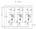
- FIG. 7 is a circuit diagram of a sensorless SRM according to a second embodiment of this invention.
- FIG. 8 is a circuit diagram of a sensorless SRM according to a third embodiment of this invention.
- FIG. 5 is a circuit diagram of a sensorless SRM according to a first embodiment of this invention.
- the sensorless SRM includes a motor driving part 90 for driving a motor through excitation of each phase of the motor in a predetermined sequence, an adding part 100 for adding the currents of each phase of the motor driving part 90, a low pass filtering part 110 for filtering the output signals from said adding part 100, a first amplifying part 60a for amplifying phase voltages V1', V2' and V3' transmitted from the filtering part 110 to a proper level, a first comparing part 70a for generating high level signals in case the output voltages VA, VB and VC of the first amplifying part 60a are higher than reference voltages Vref1, Vref2 and Vref3 through the comparison of the output voltages VA, VB and VC of the first amplifying part 60a with the reference voltage, a delaying part 50 for delaying the phase voltages V1', V2' and V3', transmitted from the filtering part 110 for certain times, a second amplifying part 60b for amplifying the output voltages from the delay part 50
- the motor driving part 90 includes the first transistor Q1 having the collector connected to a supply voltage source Vdc and the emitter connected to the cathode of a diode D6 and one terminal of a coil La, the second transistor Q2 having the collector connected to the other terminal of the coil La and the anode of the diode D7 and the emitter connected to a resistor R17, and a transistor R16 connected to the anode of the diode D6.
- the pairs of transistors Q3 and Q4, and Q5 and Q6 are connected with coils Lb and Lc, diodes D8 and D9, and D10 and D11, and resistors R18 and R19, and R20 and R21.
- the transistors Q1 and Q2 are turned off to form a current discharge flow passage in the sequence of the resistor R16, diode D6, coil La and diode D7. Thefore, the current in the resistor R16 decreases gradually while the transistors Q1 and Q2 are turning off.
- the resistor R16 developps negative voltage as shown in FIG. 6C, and the resistor R17 develops positive voltage as shown in FIG. 6B.
- the adding part 100 includes an inverter 101 connected to the cathode of the diode D6 of the motor driving part 90 for inverting the current in the resistor R16 and the adder 104 for adding the currents flowing through the resistor R22 connected to the inverter 101 and the resistor R23 connected to the emitter of the transistor Q2 of the motor driving part 90.
- adders 105 and 106 connected with interters 102 and 103 and resistors R24 and R25, and R26 and R27.
- the inverter 101 inverts the voltage on the resistor R16 and transmits the inverted voltage to the adder 104.
- the adder 104 adds the output signal from the inverter 101 and the voltage on the resistor R17.
- the output signal of the adder 104 is as shown in FIG. 6D.
- the filtering part 110 has three low pass filters 111 to 113.
- the low pass filter 111 filters the output signal of the adder 104 in order to make no discontinuity in the shape of current flowing through the winding of the SRM.
- the resultant wave pattern is as shown in FIG. 6E.
- the output signals V1', V2' and V3' of the low pass filters 111 to 113 are transmitted to the first amplifying part 60a and the delaying part 50, respectively.
- the first amplifying part 60a has the amplifiers AMP1 to AMP3, which amplify the output signals of the filtering part 110 to proper levels to transmit it to the first comparing part 70a.
- the first comparing part 70a has comparators CP1 to CP3, and compares the output signals of the first amplifier 60a with reference voltages Vref1, Vref2 and Vref3 and generates high level signals in case the output signal is higher than the reference voltages Vref1, Vref2 and Vref3.
- the delaying part 50 being an integrator type includes resistors R13 to R15 and capacitors C7 to C9.
- the signals delayed in the delaying part 50 are transmitted to the second amplifying part 60b.
- the second amplifying part 60b has amplifiers AMP4 to AMP6.
- the output signals of the delaying part 50 are amplified to proper levels and transmitted to the second comparing part 70b thereafter.
- the second comparing part 70b has comparators CP4 to CP6.
- the second comparing part 70b compares the output signals of the amplifying part 60b with reference voltages Vref4 to Vref6 to generate high level signals in case the output voltages are higher than the reference voltages Vref4 to Vref6 and low level signals in case the output voltages are lower than the reference voltages Vref4 to Vref6.
- the OR gating part 80 has OR gates OR1 to OR3 and receives the output signals from the first and the second comparing parts 70a and 70b.
- the OR gate OR1 receives the output signals of the comparator CP1 and the comparator CP4, the OR gate OR2 receives the output signals of the comparator CP2 and the comparator CP5, and the OR gate receives the output signals of the comparator CP3 and the comparator CP6.
- the output signals generated in the OR gates OR1 to OR3 are applied to the gates of the each pair of transistors Q1 and Q2, Q3 and Q4, and Q5 and Q6 of the motor driving part 90.
- the position of the rotor 1 can be detected utilizing the output signals of the OR gates OR1 to OR3.
- the advance angle of the SRM can be adjusted through the adjustment of the capacitances of the capacitors C4 to C6, of the delaying part 50.
- FIG. 7 is a circuit diagram of a motor driving part 120 of a sensorless SRM according to a second embodiment of this invention.
- pairs of transistors Q1 and Q2, Q3 and Q4 and Q5 and Q6 are connected in series, the emitters of the transistors Q1, Q3 and Q5 and the collectors of the transistors Q2, Q4 and Q5 and the collectors of the resistors R28, R29 and R30 and coils La, Lb and Lc are connected in series, respectively, the diodes D6, D8 and D10 are connected to the emitters of the transistors, Q1, Q3 and Q5 and the diodes D7, D9 and D11 are connected to the collectors of the transistors Q2, Q4 and Q6 and connected to the voltage supply source Vdc.
- the collectors of the transistors Q1, Q2 and Q3 are also connected to the voltage supply source Vdc.
- the transistors Q1 and Q2 are applied with high level of the pulse width modulation signals, the transistors Q1 and Q2 are turned-on making the current flow passage in the sequence of the current detection resistor R28 and the coil La. Therefore, the current wave pattern can be detected from the current detection resistor R28 while the transistors Q1 and Q2 are turning on.
- the transistors Q1 and Q2 are turned off making the current discharge flow passage in the sequence of the diode D6, the current detection resistor R28, the coil La and the diode D7. Therefore, the current wave pattern can be detected from the current detection resistor R28 while the transistors Q1 and Q2 are turning off.
- the current wave pattern for the windings of each phase can be detected while one pair of transistors Q1 and Q2 are turning on and off.
- FIG. 8 is a circuit diagram of a motor driving part 130 of a sensorless SRM according to a third embodiment of this invention.
- the projected part of the stator 6 is wound with single winding as shown in FIG. 2A, but the projected part of the stator 6 having two windings is described in the third embodiment.
- transistors Q7, Q8 and Q9, coils L1, L3 and L5, and current detection resistors R28, R30 and R32 connected in series, and diodes D11, D12 and D13, coils L2, L4 and L6, and current detection resistors R29, R31 and R33 connected in series, are connected between the plus terminal and minus terminal of the supply voltage source Vdc in parallel, and transistors Q7, Q8 and Q9 have the collectors connected with coils L1, L3 and L5 and the emitters connected with the current detection resistors R28, R30 and R32.
- the coil L1 and coil L2 are in mutual induction
- the coil L3 and the coil L4, and the coil L5 and the coil L6, are in mutual induction.
- the transistor Q7 is turned on when the transistor Q7 is applied with high level of the pulse width modulation signal.
- the current flow passage is formed in the sequence of the coil L1 and the current detection resistor R28 on the turn on of the transistor Q7.
- the sensorless SRM has the advantages of enabling proper operation in unfavorable conditions such as high temperature and the like as well as making the product compact by identifying the position of rotor through the detection of the change of each phase current without providing separate sensors for identifying the position of the rotor of the SRM.
Landscapes
- Engineering & Computer Science (AREA)
- Power Engineering (AREA)
- Control Of Motors That Do Not Use Commutators (AREA)
- Control Of Electric Motors In General (AREA)
Abstract

Description
- This invention relates to sensorless switched reluctance motors (hereinafter called "SRM"), more particularly to the sensorless SRMs suitable to drive the SRMs based on the position of a rotor detected through the detection of the variation of the current of each phase without providing separate sensors for identifying the position of the rotor.
- FIG. 1 shows rotor and sensors of a conventional SRM. A
rotor 1 rotates on the generation of a magnetic field thereof by fixed magnetic poles. Asensor disc 2 is mounted on the same shaft with therotor 1 to rotate together with therotor 1. Position detection sensors S1, S2 and S3 detect the condition of the light passing or blocked by thesensor disc 2 on the rotation of thesensor disc 2. Alogical circuit 5 generates phase excitation signals PH1, PH2 and PH3 on input of position detection signals from the position detection sensors S1, S2 and S3. The position detection sensors S1, S2 and S3 includeslight emitter 3 emitting light andlight receiver 4 receiving light respectively. - FIG. 2A shows a typical stator and the rotor of the SRM and FIG. 2B shows construction of a sensor disc of a conventional SRM.
- As shown in FIG. 2B, the
sensor disc 2 mounted on therotor 1 and having projections 9 and cuts 10 rotates together with therotor 1 when therotor 1 rotates. - The light emitters 3 of the position detection sensors S1, S2 and S3 emit light on the rotation of the
sensor disc 2. The light is passed or blocked by the projections 9 and thecuts 10 in thesensor disc 2. Then thelight receiver 4 of the position detection sensors S1, S2 and S3 detect the continuous intermission of light. On supply of power to the SRM, therotor 1 rotates and thesensor disc 2 mounted on therotor 1 is rotates. Then the emitted light according to the rotation of thesensor disc 2 is detected by the position detection sensors S1, S2 and S3. The light signals from above light emission are converted into a electrical signal. - The converted electrical signals are as shown in FIG. 3A.
- In FIG. 3A, (a) is output wave of the first position detection sensor S1, (b) is output wave of the second position detection sensor S2 and (c) is output wave of the third position detection sensor S3.
- Referring to FIG. 2B, the output wave of the first position detection sensor S1 is explained. A low level signal is generated during the first 30 degrees because the
light receiver 4 can receives no light. Thelight receiver 4 receives light during next 60 degrees because the light is passed, thus the position detection sensor S1 generates a high level signal. - In this way the position detection sensor S1 generates the high or low level signal.
- When the signals as in FIG. 3A are supplied to the
logical circuit 5 for generating phase excitation signals, signals as in FIG. 3B are generated from thelogical circuit 5, which drive a gate of a transistor or a base of the transistor resulting in the rotation of the motor. Different signals with the signals as in FIG. 3B can be generated by control signals(not shown) in thelogical circuit 5. - FIG. 3B shows the
rotor 1 rotating in counter clockwise direction. In this case, the power should be supplied to terminal A-A' first, to B-B' next and to C-C' third in FIG. 2A. But, in order to rotate therotor 1 in clockwise direction, the power should be supplied to terminal A-A', and to C-C' and B-B' in sequence continuously thereafter. - FIG. 4 shows changes of inductance of a coil wound on a
stator 6 according to change of phase. The inductance of the coil is the largest when there in no difference in phase ie, when the coil wound part of thestator 6 is matched with the projections 9 of the rotor, 1 and the smallest when the coil wound part of thestator 6 is positioned in 45 degrees by the phase difference with the projections 9 of therotor 1. - Generally, excitation occurs in a degrees by the phase difference in the SRM, starting the excitation at the point of inductance increase of the coil. The motor will be braked, if the excitation is started at the point of inductance decrease. In another word, when the signals detected by the
light receivers 4 are transmitted to thelogical circuit 5, thelogical circuit 5 generates the phase excitation signals PH1, PH2, and PH3 as shown in 3B and transmits these signals to terminals A-A', B-B' and C-C' shown in FIG. 2A, respectively to excite A phase winding La, B phase winding Lb and C phase winding Lc in sequence to rotate therotor 1. - However, it has problems in conventional SRM as follow. Various machining processes to mount the position detection sensors on the motors are required in order to detect the position of the rotor, Thus the production processes are complicated that much. And more space to mount the position detection sensors inside or outside of the motors makes the motors larger. Special sensors are required in case the motor should be operated in high temperature where ordinary sensors are not operative. Sensors like photo-interrupt element are unable to operate when the motors contain refrigerant or lubrication oil like compressors.
- The object of this invention is to provide sensorless SRMs suitable for controlling of the operation of the SRMs through the detection of the changes of the current in each phase without employing the sensor disc and position detection sensors for the detection of the position of a rotor.
- This and other objects of this invention can be achieved by providing a sensorless switched reluctance motor comprising :
- a motor driving part for driving the motor by exciting phases of the motor in a predetermined sequence ;
- an adding part for adding the currents of each phase;
- a low pass filtering part for filtering the output signals from said adding parts ;
- a first amplifying part for amplifying output voltages from said low pass filtering part to first proper levels ;
- a first comparing part for comparing output voltages of said first amplifying part with first references voltages respectively, to generate a high level signal in case the output voltage of said first amplifying part is higher than the first reference voltage and a low level signal in case the output voltage of said first amplifying part is lower than the first reference voltage ;
- a delaying part for delaying the output voltages from said low pass filtering part for predetermined times ;
- a second amplifying part for amplifying the output voltages from said delaying part to second proper levels ;
- a second comparing part for comparing output voltages from said second amplifying part with second reference voltages respectively, to generate the high level signal in case the output voltage of said second amplifying part is higher than the second reference voltage and the low level signal in case the output voltage of said second amplifying part is lower than the second reference voltage ; and
- an OR gating part for logically operating the output signals from said first comparing part and the output signals from said second comparing part.
- FIG. 1 shows a rotor and sensors of a conventional SRM.
- FIG. 2A shows a stator and the rotor of the conventional SRM.
- FIG. 2B shows a sensor disc of the conventional SRM.
- FIG. 3A and 3B show the wave patterns of each part of FIG. 2.
- FIGs. 4A, 4B and 4C show changes of inductance of each phase according to the changes of rotation angle.
- FIG. 5 is a circuit diagram of a sensorless SRM according to a first embodiment of this invention.
- FIGs. 6A to 6E show wave patterns of each part of FIG. 5.
- FIG. 7 is a circuit diagram of a sensorless SRM according to a second embodiment of this invention.
- FIG. 8 is a circuit diagram of a sensorless SRM according to a third embodiment of this invention.
- FIG. 5 is a circuit diagram of a sensorless SRM according to a first embodiment of this invention.
- The sensorless SRM includes a motor driving part 90 for driving a motor through excitation of each phase of the motor in a predetermined sequence, an adding part 100 for adding the currents of each phase of the motor driving part 90, a low pass filtering part 110 for filtering the output signals from said adding part 100, a first amplifying part 60a for amplifying phase voltages V1', V2' and V3' transmitted from the filtering part 110 to a proper level, a first comparing part 70a for generating high level signals in case the output voltages VA, VB and VC of the first amplifying part 60a are higher than reference voltages Vref1, Vref2 and Vref3 through the comparison of the output voltages VA, VB and VC of the first amplifying part 60a with the reference voltage, a delaying part 50 for delaying the phase voltages V1', V2' and V3', transmitted from the filtering part 110 for certain times, a second amplifying part 60b for amplifying the output voltages from the delay part 50 to proper levels, a second comparing part 70b for generating high level signals in case the phase voltages VA', VB' and VC' transmitted from the second amplifying part 60b are higher than reference voltages Vref4, Vref5 and Vref6 through the comparison of the phase voltages with the reference voltages Vref4, Vref5 and Vref6 and low level signals in other cases, and an OR gating part 80 for OR gating the output signals from the first comparing part 70a and the second comparing part 70b.
- The
motor driving part 90 includes the first transistor Q1 having the collector connected to a supply voltage source Vdc and the emitter connected to the cathode of a diode D6 and one terminal of a coil La, the second transistor Q2 having the collector connected to the other terminal of the coil La and the anode of the diode D7 and the emitter connected to a resistor R17, and a transistor R16 connected to the anode of the diode D6. In this manner, the pairs of transistors Q3 and Q4, and Q5 and Q6 are connected with coils Lb and Lc, diodes D8 and D9, and D10 and D11, and resistors R18 and R19, and R20 and R21. - When a high level signal of the pulse width modulation signal as shown in FIG. 6A is applied to the bases of the transistors Q1 and Q2, the transistors Q1 and Q2 are turned on. Then, the passage of current is formed in the sequence of the coil La and the resistor R17 and the current in the resistor R17 increases gradually while the transistors Q1 and Q2 are turning on.
- In this time, if the low level signal of the pulse width modulation signal is applied to the bases of the transistors Q1 and Q2, the transistors Q1 and Q2 are turned off to form a current discharge flow passage in the sequence of the resistor R16, diode D6, coil La and diode D7. Thefore, the current in the resistor R16 decreases gradually while the transistors Q1 and Q2 are turning off.
- When the high level signal of the pulse width modulation signal is applied again to the bases of the transistors Q1 and Q2 during the decrease of the current, the transistors Q1 and Q2 are turned on again making the current in the resistor R17 flow again. Repetition of this operation results in the voltage on the resistor R17 as shown in FIG. 6B and the voltage on the resistor R16 as shown in FIG. 6C.
- Accordingly, due to the direction of the current, the resistor R16 developps negative voltage as shown in FIG. 6C, and the resistor R17 develops positive voltage as shown in FIG. 6B.
- The adding
part 100 includes aninverter 101 connected to the cathode of the diode D6 of themotor driving part 90 for inverting the current in the resistor R16 and theadder 104 for adding the currents flowing through the resistor R22 connected to theinverter 101 and the resistor R23 connected to the emitter of the transistor Q2 of themotor driving part 90. In this manner,adders interters - The
inverter 101 inverts the voltage on the resistor R16 and transmits the inverted voltage to theadder 104. Theadder 104 adds the output signal from theinverter 101 and the voltage on the resistor R17. The output signal of theadder 104 is as shown in FIG. 6D. - The
filtering part 110 has three low pass filters 111 to 113. Thelow pass filter 111 filters the output signal of theadder 104 in order to make no discontinuity in the shape of current flowing through the winding of the SRM. The resultant wave pattern is as shown in FIG. 6E. - The output signals V1', V2' and V3' of the low pass filters 111 to 113 are transmitted to the first amplifying
part 60a and the delayingpart 50, respectively. - The
first amplifying part 60a has the amplifiers AMP1 to AMP3, which amplify the output signals of thefiltering part 110 to proper levels to transmit it to the first comparing part 70a. - The first comparing part 70a has comparators CP1 to CP3, and compares the output signals of the
first amplifier 60a with reference voltages Vref1, Vref2 and Vref3 and generates high level signals in case the output signal is higher than the reference voltages Vref1, Vref2 and Vref3. - The delaying
part 50 being an integrator type includes resistors R13 to R15 and capacitors C7 to C9. The signals delayed in the delayingpart 50 are transmitted to thesecond amplifying part 60b. - The
second amplifying part 60b has amplifiers AMP4 to AMP6. In thesecond amplifier 60b, the output signals of the delayingpart 50 are amplified to proper levels and transmitted to the second comparingpart 70b thereafter. - The second comparing
part 70b has comparators CP4 to CP6. The second comparingpart 70b, compares the output signals of the amplifyingpart 60b with reference voltages Vref4 to Vref6 to generate high level signals in case the output voltages are higher than the reference voltages Vref4 to Vref6 and low level signals in case the output voltages are lower than the reference voltages Vref4 to Vref6. - The OR gating
part 80 has OR gates OR1 to OR3 and receives the output signals from the first and the second comparingparts 70a and 70b. - The OR gate OR1 receives the output signals of the comparator CP1 and the comparator CP4, the OR gate OR2 receives the output signals of the comparator CP2 and the comparator CP5, and the OR gate receives the output signals of the comparator CP3 and the comparator CP6.
- The output signals generated in the OR gates OR1 to OR3 are applied to the gates of the each pair of transistors Q1 and Q2, Q3 and Q4, and Q5 and Q6 of the
motor driving part 90. - Thus, the position of the
rotor 1 can be detected utilizing the output signals of the OR gates OR1 to OR3. The advance angle of the SRM can be adjusted through the adjustment of the capacitances of the capacitors C4 to C6, of the delayingpart 50. - FIG. 7 is a circuit diagram of a
motor driving part 120 of a sensorless SRM according to a second embodiment of this invention. - In FIG. 7, pairs of transistors Q1 and Q2, Q3 and Q4 and Q5 and Q6 are connected in series, the emitters of the transistors Q1, Q3 and Q5 and the collectors of the transistors Q2, Q4 and Q5 and the collectors of the resistors R28, R29 and R30 and coils La, Lb and Lc are connected in series, respectively, the diodes D6, D8 and D10 are connected to the emitters of the transistors, Q1, Q3 and Q5 and the diodes D7, D9 and D11 are connected to the collectors of the transistors Q2, Q4 and Q6 and connected to the voltage supply source Vdc. The collectors of the transistors Q1, Q2 and Q3 are also connected to the voltage supply source Vdc.
- It is shown that it is possible to detect the current flowing in each phase with only one current detection resistor R28, R29 or R30 during the turn on and off of the pairs of transistors Q1 and Q2, Q3 and Q4, and Q5 and Q6.
- For example, if the bases of the transistors Q1 and Q2 are applied with high level of the pulse width modulation signals, the transistors Q1 and Q2 are turned-on making the current flow passage in the sequence of the current detection resistor R28 and the coil La. Therefore, the current wave pattern can be detected from the current detection resistor R28 while the transistors Q1 and Q2 are turning on.
- In this time, if the bases of the transistors Q1 and Q2 are applied with low level of the pulse width modulation signals, the transistors Q1 and Q2 are turned off making the current discharge flow passage in the sequence of the diode D6, the current detection resistor R28, the coil La and the diode D7. Therefore, the current wave pattern can be detected from the current detection resistor R28 while the transistors Q1 and Q2 are turning off.
- In conclusion, the current wave pattern for the windings of each phase can be detected while one pair of transistors Q1 and Q2 are turning on and off.
- FIG. 8 is a circuit diagram of a
motor driving part 130 of a sensorless SRM according to a third embodiment of this invention. - Up to now, the projected part of the
stator 6 is wound with single winding as shown in FIG. 2A, but the projected part of thestator 6 having two windings is described in the third embodiment. - As shown in FIG. 8, transistors Q7, Q8 and Q9, coils L1, L3 and L5, and current detection resistors R28, R30 and R32 connected in series, and diodes D11, D12 and D13, coils L2, L4 and L6, and current detection resistors R29, R31 and R33 connected in series, are connected between the plus terminal and minus terminal of the supply voltage source Vdc in parallel, and transistors Q7, Q8 and Q9 have the collectors connected with coils L1, L3 and L5 and the emitters connected with the current detection resistors R28, R30 and R32.
- The coil L1 and coil L2 are in mutual induction, the coil L3 and the coil L4, and the coil L5 and the coil L6, are in mutual induction. The transistor Q7 is turned on when the transistor Q7 is applied with high level of the pulse width modulation signal. The current flow passage is formed in the sequence of the coil L1 and the current detection resistor R28 on the turn on of the transistor Q7.
- Even though current flows in the coil L2 by the self-induction thereon, current does not flow in the coil L2 due to the diode 11 positioned in the reverse direction. In this condition, if the base of the transistor Q7 is applied with low level of the pulse width modulation signal to turn off the transistor Q7, the current discharge flow passage is formed in the sequence of the current detection resistor R29, the coil L2 and the diode D11.
- According to this invention, the sensorless SRM has the advantages of enabling proper operation in unfavorable conditions such as high temperature and the like as well as making the product compact by identifying the position of rotor through the detection of the change of each phase current without providing separate sensors for identifying the position of the rotor of the SRM.
- Although the invention has been described in conjunction with specific embodiments, it is evident that many alternatives and variations will be apparent to those skilled in the art in light of the foregoing description. Accordingly, the invention is intended to embrace all of the alternatives and variations that fall within the spirit and scope of the appended claims.
Claims (7)
- A sensorless switched reluctance motor comprising:a motor driving part (90) for driving the motor by exciting phases of the motor in a predetermined sequence ;an adding part (100) for adding the currents of each phase ;a low pass filtering part (110) for filtering the output signals from said adding parts (100) ;a first amplifying part (60a) for amplifying output voltages from said low pass filtering part (110) to first proper levels ;a first comparing part (70a) for comparing output voltages of said first amplifying part (60a) with first references voltages respectively, to generate a high level signal in case the output voltage of said first amplifying part (60a) is higher than the first reference voltage and a low level signal in case the output voltage of said first amplifying part (60a) is lower than the first reference voltage ;a delaying part (50) for delaying the output voltages from said low pass filtering part (110) for predetermined times ;a second amplifying part (60b) for amplifying the output voltages from said delaying part (50) to second proper levels ;a second comparing part (70b) for comparing output voltages from said second amplifying part (60b) with second reference voltages respectively, to generate the high level signal in case the output voltage of said second amplifying part (60b) is higher than the second reference voltage and the low level signal in case the output voltage of said second amplifying part (60b) is lower than the second reference voltage ; andan OR gating part (80) for logically operating the output signals from said first comparing part (70a) and the output signals from said second comparing part (70b).
- A sensorless switched reluctance motor as claimed in claim 1, wherein said adding part (100) includes a plurality of blocks, each block having an inverter (101) for inverting the current flowing through a first current detecting resistor (R16), said inverter (101) being connected with a cathode of a diode (D6) of said motor driving part (90), and an adder (104) for adding the output signal of said inverter (101) and a voltage applied to a second current detecting resistor (R17) of said motor driving part (90).
- A sensorless switched reluctance motor as claimed in claim 1, wherein said low pass filtering part (110) includes a plurality of low pass filters (111, 112, 113).
- A sensorless switched reluctance motor as claimed in claim 1, wherein said motor driving part (90) includes a plurality of blocks (120), each block having one pair of switching means (Q1-Q6) connected in series, current detection resistors (R28-R30) and a coil (La, Lb, Lc) connected in parallel between said one pair of switching means (Q1-Q6).
- A sensorless switched reluctance motor as claimed in claim 2, wherein said one pair of switching means (Q1, Q2) are positioned between a plus terminal and a minus terminal of a supply voltage source.
- A sensorless switched reluctance motor as claimed in claim 5, further including a first diode (D6) which has a first anode connected to the minus terminal of the supply voltage source and a first cathode connected to the current detection resistor (R16), and a second diode (D7) which has a second anode connected to a coil (La) and a second cathode connected to the plus terminal of the supply voltage source.
- A sensorless switched reluctance motor as claimed in claim 1, wherein said motor driving part (90) includes a plurality of blocks (130), each block having a first coil (L1, L3, L5), a switching means (Q7, Q8, Q9) and a first current detection resistor (R28, R30, R32) connected in series between the plus terminal and the minus terminal of the supply voltage source, and a diode (D11, D12, D13), a second coil (L2, L4, L6) and a second current detection resistor (R29, R31, R33) connected in series, to be thereby connected in parallel.
Applications Claiming Priority (7)
| Application Number | Priority Date | Filing Date | Title |
|---|---|---|---|
| KR2472592 | 1992-12-17 | ||
| KR1019920024724A KR950008420B1 (en) | 1992-12-17 | 1992-12-17 | Sensorless srm |
| KR2472492 | 1992-12-17 | ||
| KR1019920024725A KR950015171B1 (en) | 1992-12-17 | 1992-12-17 | Sensorless srm |
| KR1019930001155A KR950010666B1 (en) | 1993-01-29 | 1993-01-29 | Switched reluctance motor driving circuit |
| KR1105593 | 1993-01-29 | ||
| EP93403041A EP0603071B1 (en) | 1992-12-17 | 1993-12-15 | Sensorless switched reluctance motor |
Related Parent Applications (1)
| Application Number | Title | Priority Date | Filing Date |
|---|---|---|---|
| EP93403041.2 Division | 1993-12-15 |
Publications (2)
| Publication Number | Publication Date |
|---|---|
| EP0784377A1 true EP0784377A1 (en) | 1997-07-16 |
| EP0784377B1 EP0784377B1 (en) | 1999-07-14 |
Family
ID=27348892
Family Applications (2)
| Application Number | Title | Priority Date | Filing Date |
|---|---|---|---|
| EP97400468A Expired - Lifetime EP0784377B1 (en) | 1992-12-17 | 1993-12-15 | Switched reluctance motor without rotor position sensor |
| EP93403041A Expired - Lifetime EP0603071B1 (en) | 1992-12-17 | 1993-12-15 | Sensorless switched reluctance motor |
Family Applications After (1)
| Application Number | Title | Priority Date | Filing Date |
|---|---|---|---|
| EP93403041A Expired - Lifetime EP0603071B1 (en) | 1992-12-17 | 1993-12-15 | Sensorless switched reluctance motor |
Country Status (3)
| Country | Link |
|---|---|
| US (1) | US5589751A (en) |
| EP (2) | EP0784377B1 (en) |
| DE (2) | DE69325670T2 (en) |
Cited By (2)
| Publication number | Priority date | Publication date | Assignee | Title |
|---|---|---|---|---|
| CN104201948A (en) * | 2014-09-04 | 2014-12-10 | 燕山大学 | Control device and method of position-free sensor of switched reluctance motor |
| US9722517B2 (en) | 2014-04-01 | 2017-08-01 | Mcmaster University | Systems and methods for rotor position determination |
Families Citing this family (29)
| Publication number | Priority date | Publication date | Assignee | Title |
|---|---|---|---|---|
| GB9505655D0 (en) * | 1995-03-21 | 1995-05-10 | Switched Reluctance Drives Ltd | Torque improvements in reluctance motors |
| US5691591A (en) * | 1995-05-19 | 1997-11-25 | Itt Automotive Electrical Systems Inc. | Switched reluctance motor with indirect position sensing and magnetic brake |
| US5821713A (en) * | 1995-09-11 | 1998-10-13 | Advanced Motion Controls, Inc. | Commutation position detection system and method |
| GB9525952D0 (en) * | 1995-12-19 | 1996-02-21 | Switched Reluctance Drives Ltd | Sensorless rotor position monitoring in reluctance machines |
| US6359412B1 (en) * | 1996-04-09 | 2002-03-19 | Hamilton Sundstrand Corporation | Commutation apparatus and method for a four state sensorless switched reluctance machine system utilizing machine winding current sensing |
| US6107772A (en) * | 1997-09-26 | 2000-08-22 | Dana Corporation | Sensorless switched reluctance motor control |
| KR100259375B1 (en) * | 1997-11-10 | 2000-06-15 | 윤종용 | A device for and a method of driving sensorless srm |
| SG106576A1 (en) * | 1999-01-11 | 2004-10-29 | Switched Reluctance Drives Ltd | Rotor position detection in switched reluctance machines |
| US6157150A (en) * | 1999-01-15 | 2000-12-05 | Semipower Systems, Inc. | Brushless sensorless DC motor assembly with precisely controllable positioning |
| US6242874B1 (en) * | 1999-10-27 | 2001-06-05 | Dana Corporation | Phase commutation of a switched reluctance motor by single phase sensing of inductance |
| CA2288581A1 (en) | 1999-11-05 | 2001-05-05 | Hui Li | Three-phase current sensor and estimator |
| GB9929655D0 (en) * | 1999-12-15 | 2000-02-09 | Switched Reluctance Drives Ltd | Rotor position monitoring of a switched reluctance drive |
| US6301136B1 (en) | 2000-07-19 | 2001-10-09 | Honeywell International Inc. | Floating flame controller |
| DE10156243A1 (en) * | 2001-11-15 | 2003-06-05 | Bosch Gmbh Robert | Electronically commutated motor |
| US6487769B2 (en) | 2000-11-30 | 2002-12-03 | Emerson Electric Co. | Method and apparatus for constructing a segmented stator |
| US6597078B2 (en) | 2000-12-04 | 2003-07-22 | Emerson Electric Co. | Electric power steering system including a permanent magnet motor |
| US6584813B2 (en) | 2001-03-26 | 2003-07-01 | Emerson Electric Co. | Washing machine including a segmented stator switched reluctance motor |
| US6744166B2 (en) | 2001-01-04 | 2004-06-01 | Emerson Electric Co. | End cap assembly for a switched reluctance electric machine |
| US7012350B2 (en) | 2001-01-04 | 2006-03-14 | Emerson Electric Co. | Segmented stator switched reluctance machine |
| US6897591B2 (en) | 2001-03-26 | 2005-05-24 | Emerson Electric Co. | Sensorless switched reluctance electric machine with segmented stator |
| US6700284B2 (en) | 2001-03-26 | 2004-03-02 | Emerson Electric Co. | Fan assembly including a segmented stator switched reluctance fan motor |
| US6803740B2 (en) * | 2002-10-25 | 2004-10-12 | Delphi Technologies, Inc. | Method and apparatus for determining phase current of switched reluctance electric machines |
| KR101152083B1 (en) * | 2003-04-24 | 2012-06-11 | 니덱 에스알 드라이브즈 리미티드 | Rotor position detector of a switched reluctance machine |
| US20050153932A1 (en) * | 2003-10-08 | 2005-07-14 | Sprengers Erik D. | Controlled muscle relaxation |
| DE102004041753A1 (en) * | 2004-08-28 | 2006-03-02 | Zf Friedrichshafen Ag | Selector drive for automated manual transmissions of motor vehicles |
| US7050929B2 (en) * | 2004-10-21 | 2006-05-23 | Shop Vac | System and method of ensuring legitimacy of a sensor signal received from a rotor position sensor in a motor |
| US8339078B2 (en) * | 2009-07-13 | 2012-12-25 | The City University Of Hong Kong | Apparatus and method for providing information relating to a motor |
| CN110022098B (en) * | 2019-02-12 | 2020-11-06 | 湖南科技大学 | Switched reluctance motor position sensorless control method and device based on phase inductance unsaturated zone positioning |
| CN109951115B (en) * | 2019-04-08 | 2021-08-31 | 东莞市诺必然智能科技有限公司 | Self-adaptive control method for rotating speed of direct-current brushless motor |
Citations (3)
| Publication number | Priority date | Publication date | Assignee | Title |
|---|---|---|---|---|
| US4595865A (en) * | 1985-10-31 | 1986-06-17 | General Electric Company | Current-sensing scheme for switched reluctance motor drives |
| US4896088A (en) * | 1989-03-31 | 1990-01-23 | General Electric Company | Fault-tolerant switched reluctance machine |
| US5051680A (en) * | 1989-12-08 | 1991-09-24 | Sundstrand Corporation | Simple starting sequence for variable reluctance motors without rotor position sensor |
Family Cites Families (10)
| Publication number | Priority date | Publication date | Assignee | Title |
|---|---|---|---|---|
| FR2385257A1 (en) * | 1977-03-25 | 1978-10-20 | Alsthom Cgee | DEVICE FOR ELABORATING PHASE REFERENCE SIGNALS FOR THE CONTROL OF THE IGNITION PULSES OF THE THYRISTORS OF A GRAETZ BRIDGE OPERATING AT VARIABLE FREQUENCY |
| BR8205838A (en) * | 1981-01-26 | 1983-01-11 | Reginald Kenneth Payne | PROXIMITY DETECTOR CIRCUIT SYSTEM ESPECIALLY FOR ELEVATOR DOORS |
| US4353016A (en) * | 1981-04-22 | 1982-10-05 | Minnesota Mining And Manufacturing Company | Linear motor control system for brushless DC motor |
| US4401934A (en) * | 1981-08-07 | 1983-08-30 | The United States Of America As Represented By The Administrator Of The National Aeronautics And Space Administration | Adaptive control system for line-commutated inverters |
| US4641066A (en) * | 1984-10-04 | 1987-02-03 | Nippondenso Co., Ltd. | Control apparatus for brushless motor |
| US4777419A (en) * | 1987-01-28 | 1988-10-11 | Emerson Electric Co. | Control apparatus and method for operating a switched reluctance motor |
| US5144231A (en) * | 1988-09-30 | 1992-09-01 | Jeffrey Tenenbaum | Eddy current detector for detecting an object with offset compensation |
| JP2568737B2 (en) * | 1989-07-26 | 1997-01-08 | 松下電器産業株式会社 | Drive device for commutatorless motor |
| JPH0681542B2 (en) * | 1989-09-16 | 1994-10-12 | 株式会社東芝 | Brushless motor control circuit |
| US5291115A (en) * | 1992-09-25 | 1994-03-01 | The Texas A&M University System | Method and apparatus for sensing the rotor position of a switched reluctance motor without a shaft position sensor |
-
1993
- 1993-12-15 EP EP97400468A patent/EP0784377B1/en not_active Expired - Lifetime
- 1993-12-15 DE DE69325670T patent/DE69325670T2/en not_active Expired - Fee Related
- 1993-12-15 DE DE69314612T patent/DE69314612T2/en not_active Expired - Fee Related
- 1993-12-15 EP EP93403041A patent/EP0603071B1/en not_active Expired - Lifetime
- 1993-12-16 US US08/167,361 patent/US5589751A/en not_active Expired - Lifetime
Patent Citations (3)
| Publication number | Priority date | Publication date | Assignee | Title |
|---|---|---|---|---|
| US4595865A (en) * | 1985-10-31 | 1986-06-17 | General Electric Company | Current-sensing scheme for switched reluctance motor drives |
| US4896088A (en) * | 1989-03-31 | 1990-01-23 | General Electric Company | Fault-tolerant switched reluctance machine |
| US5051680A (en) * | 1989-12-08 | 1991-09-24 | Sundstrand Corporation | Simple starting sequence for variable reluctance motors without rotor position sensor |
Cited By (3)
| Publication number | Priority date | Publication date | Assignee | Title |
|---|---|---|---|---|
| US9722517B2 (en) | 2014-04-01 | 2017-08-01 | Mcmaster University | Systems and methods for rotor position determination |
| CN104201948A (en) * | 2014-09-04 | 2014-12-10 | 燕山大学 | Control device and method of position-free sensor of switched reluctance motor |
| CN104201948B (en) * | 2014-09-04 | 2017-04-12 | 燕山大学 | Control device and method of position-free sensor of switched reluctance motor |
Also Published As
| Publication number | Publication date |
|---|---|
| EP0603071B1 (en) | 1997-10-15 |
| DE69314612D1 (en) | 1997-11-20 |
| EP0603071A3 (en) | 1994-10-05 |
| DE69314612T2 (en) | 1998-02-12 |
| EP0784377B1 (en) | 1999-07-14 |
| US5589751A (en) | 1996-12-31 |
| EP0603071A2 (en) | 1994-06-22 |
| DE69325670T2 (en) | 1999-12-23 |
| DE69325670D1 (en) | 1999-08-19 |
Similar Documents
| Publication | Publication Date | Title |
|---|---|---|
| EP0784377B1 (en) | Switched reluctance motor without rotor position sensor | |
| US6879120B2 (en) | Speed control circuit of brushless DC fan motor | |
| US5291115A (en) | Method and apparatus for sensing the rotor position of a switched reluctance motor without a shaft position sensor | |
| US4603283A (en) | Variable speed control for a brushless direct current motor | |
| US5376866A (en) | Motor controls, refrigeration systems and methods of motor operation and control | |
| US5125067A (en) | Motor controls, refrigeration systems and methods of motor operation and control | |
| US5006774A (en) | Torque angle control system for controlling the torque angle of a permanent magnet synchronous motor | |
| WO1991002401A1 (en) | A method and a device for sensorless control of a reluctance motor | |
| US5339013A (en) | Method and apparatus for driving a brushless motor including varying the duty cycle in response to variations in the rotational speed | |
| US20050030002A1 (en) | Determining rotation of a freewheeling motor | |
| US6249101B1 (en) | Start-up procedure for brushless DC motors having position sensors with angular resolution lower than the resolution of the driving system | |
| US20030042863A1 (en) | Method and apparatus for controlling synchronous motor | |
| US6256181B1 (en) | Fan drive device | |
| US6249095B1 (en) | Polyphase motor driving apparatus, polyphase motor driving apparatus driving method and polyphase motor system | |
| KR100292776B1 (en) | Drive of brushless dc motor | |
| US6969962B2 (en) | DC motor drive circuit | |
| US7282876B2 (en) | System for driving brushless DC motor and method of driving same | |
| US8217609B1 (en) | Circuit for forming phase shifted signals for three phase BLDC motors | |
| KR0132502B1 (en) | Rotor positino detecting method of switched reluctance | |
| KR100228716B1 (en) | Driving control method of a switched reluctance motor | |
| US6759819B2 (en) | Rotation detection circuit of a dc brushless motor using a fixed bias voltage | |
| KR950010666B1 (en) | Switched reluctance motor driving circuit | |
| JP3402700B2 (en) | Operating method of brushless motor | |
| JP2000083393A (en) | Rotor position detecting device for sensorless motor | |
| KR940009210B1 (en) | Device for driving brushless motor |
Legal Events
| Date | Code | Title | Description |
|---|---|---|---|
| PUAI | Public reference made under article 153(3) epc to a published international application that has entered the european phase |
Free format text: ORIGINAL CODE: 0009012 |
|
| 17P | Request for examination filed |
Effective date: 19970305 |
|
| AC | Divisional application: reference to earlier application |
Ref document number: 603071 Country of ref document: EP |
|
| AK | Designated contracting states |
Kind code of ref document: A1 Designated state(s): DE FR GB |
|
| GRAG | Despatch of communication of intention to grant |
Free format text: ORIGINAL CODE: EPIDOS AGRA |
|
| 17Q | First examination report despatched |
Effective date: 19981104 |
|
| GRAG | Despatch of communication of intention to grant |
Free format text: ORIGINAL CODE: EPIDOS AGRA |
|
| GRAH | Despatch of communication of intention to grant a patent |
Free format text: ORIGINAL CODE: EPIDOS IGRA |
|
| GRAH | Despatch of communication of intention to grant a patent |
Free format text: ORIGINAL CODE: EPIDOS IGRA |
|
| GRAA | (expected) grant |
Free format text: ORIGINAL CODE: 0009210 |
|
| AC | Divisional application: reference to earlier application |
Ref document number: 603071 Country of ref document: EP |
|
| AK | Designated contracting states |
Kind code of ref document: B1 Designated state(s): DE FR GB |
|
| REF | Corresponds to: |
Ref document number: 69325670 Country of ref document: DE Date of ref document: 19990819 |
|
| ET | Fr: translation filed | ||
| PLBE | No opposition filed within time limit |
Free format text: ORIGINAL CODE: 0009261 |
|
| STAA | Information on the status of an ep patent application or granted ep patent |
Free format text: STATUS: NO OPPOSITION FILED WITHIN TIME LIMIT |
|
| 26N | No opposition filed | ||
| REG | Reference to a national code |
Ref country code: GB Ref legal event code: IF02 |
|
| PGFP | Annual fee paid to national office [announced via postgrant information from national office to epo] |
Ref country code: FR Payment date: 20081212 Year of fee payment: 16 |
|
| PGFP | Annual fee paid to national office [announced via postgrant information from national office to epo] |
Ref country code: DE Payment date: 20081211 Year of fee payment: 16 |
|
| PGFP | Annual fee paid to national office [announced via postgrant information from national office to epo] |
Ref country code: GB Payment date: 20081210 Year of fee payment: 16 |
|
| GBPC | Gb: european patent ceased through non-payment of renewal fee |
Effective date: 20091215 |
|
| REG | Reference to a national code |
Ref country code: FR Ref legal event code: ST Effective date: 20100831 |
|
| PG25 | Lapsed in a contracting state [announced via postgrant information from national office to epo] |
Ref country code: FR Free format text: LAPSE BECAUSE OF NON-PAYMENT OF DUE FEES Effective date: 20091231 |
|
| PG25 | Lapsed in a contracting state [announced via postgrant information from national office to epo] |
Ref country code: DE Free format text: LAPSE BECAUSE OF NON-PAYMENT OF DUE FEES Effective date: 20100701 |
|
| PG25 | Lapsed in a contracting state [announced via postgrant information from national office to epo] |
Ref country code: GB Free format text: LAPSE BECAUSE OF NON-PAYMENT OF DUE FEES Effective date: 20091215 |