EP0741447A2 - Circuit and method for controlling a synchronous recifier converter - Google Patents
Circuit and method for controlling a synchronous recifier converter Download PDFInfo
- Publication number
- EP0741447A2 EP0741447A2 EP96302833A EP96302833A EP0741447A2 EP 0741447 A2 EP0741447 A2 EP 0741447A2 EP 96302833 A EP96302833 A EP 96302833A EP 96302833 A EP96302833 A EP 96302833A EP 0741447 A2 EP0741447 A2 EP 0741447A2
- Authority
- EP
- European Patent Office
- Prior art keywords
- rectifier
- output
- switching circuitry
- recited
- circuitry
- Prior art date
- Legal status (The legal status is an assumption and is not a legal conclusion. Google has not performed a legal analysis and makes no representation as to the accuracy of the status listed.)
- Withdrawn
Links
Images


Classifications
-
- H—ELECTRICITY
- H02—GENERATION; CONVERSION OR DISTRIBUTION OF ELECTRIC POWER
- H02M—APPARATUS FOR CONVERSION BETWEEN AC AND AC, BETWEEN AC AND DC, OR BETWEEN DC AND DC, AND FOR USE WITH MAINS OR SIMILAR POWER SUPPLY SYSTEMS; CONVERSION OF DC OR AC INPUT POWER INTO SURGE OUTPUT POWER; CONTROL OR REGULATION THEREOF
- H02M3/00—Conversion of dc power input into dc power output
- H02M3/02—Conversion of dc power input into dc power output without intermediate conversion into ac
- H02M3/04—Conversion of dc power input into dc power output without intermediate conversion into ac by static converters
- H02M3/10—Conversion of dc power input into dc power output without intermediate conversion into ac by static converters using discharge tubes with control electrode or semiconductor devices with control electrode
- H02M3/145—Conversion of dc power input into dc power output without intermediate conversion into ac by static converters using discharge tubes with control electrode or semiconductor devices with control electrode using devices of a triode or transistor type requiring continuous application of a control signal
- H02M3/155—Conversion of dc power input into dc power output without intermediate conversion into ac by static converters using discharge tubes with control electrode or semiconductor devices with control electrode using devices of a triode or transistor type requiring continuous application of a control signal using semiconductor devices only
- H02M3/156—Conversion of dc power input into dc power output without intermediate conversion into ac by static converters using discharge tubes with control electrode or semiconductor devices with control electrode using devices of a triode or transistor type requiring continuous application of a control signal using semiconductor devices only with automatic control of output voltage or current, e.g. switching regulators
- H02M3/1563—Conversion of dc power input into dc power output without intermediate conversion into ac by static converters using discharge tubes with control electrode or semiconductor devices with control electrode using devices of a triode or transistor type requiring continuous application of a control signal using semiconductor devices only with automatic control of output voltage or current, e.g. switching regulators without using an external clock
-
- H—ELECTRICITY
- H02—GENERATION; CONVERSION OR DISTRIBUTION OF ELECTRIC POWER
- H02J—CIRCUIT ARRANGEMENTS OR SYSTEMS FOR SUPPLYING OR DISTRIBUTING ELECTRIC POWER; SYSTEMS FOR STORING ELECTRIC ENERGY
- H02J1/00—Circuit arrangements for dc mains or dc distribution networks
- H02J1/001—Hot plugging or unplugging of load or power modules to or from power distribution networks
-
- H—ELECTRICITY
- H02—GENERATION; CONVERSION OR DISTRIBUTION OF ELECTRIC POWER
- H02J—CIRCUIT ARRANGEMENTS OR SYSTEMS FOR SUPPLYING OR DISTRIBUTING ELECTRIC POWER; SYSTEMS FOR STORING ELECTRIC ENERGY
- H02J1/00—Circuit arrangements for dc mains or dc distribution networks
- H02J1/10—Parallel operation of dc sources
- H02J1/102—Parallel operation of dc sources being switching converters
-
- H—ELECTRICITY
- H02—GENERATION; CONVERSION OR DISTRIBUTION OF ELECTRIC POWER
- H02M—APPARATUS FOR CONVERSION BETWEEN AC AND AC, BETWEEN AC AND DC, OR BETWEEN DC AND DC, AND FOR USE WITH MAINS OR SIMILAR POWER SUPPLY SYSTEMS; CONVERSION OF DC OR AC INPUT POWER INTO SURGE OUTPUT POWER; CONTROL OR REGULATION THEREOF
- H02M3/00—Conversion of dc power input into dc power output
- H02M3/22—Conversion of dc power input into dc power output with intermediate conversion into ac
- H02M3/24—Conversion of dc power input into dc power output with intermediate conversion into ac by static converters
- H02M3/28—Conversion of dc power input into dc power output with intermediate conversion into ac by static converters using discharge tubes with control electrode or semiconductor devices with control electrode to produce the intermediate ac
- H02M3/325—Conversion of dc power input into dc power output with intermediate conversion into ac by static converters using discharge tubes with control electrode or semiconductor devices with control electrode to produce the intermediate ac using devices of a triode or a transistor type requiring continuous application of a control signal
- H02M3/335—Conversion of dc power input into dc power output with intermediate conversion into ac by static converters using discharge tubes with control electrode or semiconductor devices with control electrode to produce the intermediate ac using devices of a triode or a transistor type requiring continuous application of a control signal using semiconductor devices only
- H02M3/33569—Conversion of dc power input into dc power output with intermediate conversion into ac by static converters using discharge tubes with control electrode or semiconductor devices with control electrode to produce the intermediate ac using devices of a triode or a transistor type requiring continuous application of a control signal using semiconductor devices only having several active switching elements
- H02M3/33576—Conversion of dc power input into dc power output with intermediate conversion into ac by static converters using discharge tubes with control electrode or semiconductor devices with control electrode to produce the intermediate ac using devices of a triode or a transistor type requiring continuous application of a control signal using semiconductor devices only having several active switching elements having at least one active switching element at the secondary side of an isolation transformer
- H02M3/33584—Bidirectional converters
-
- H—ELECTRICITY
- H02—GENERATION; CONVERSION OR DISTRIBUTION OF ELECTRIC POWER
- H02M—APPARATUS FOR CONVERSION BETWEEN AC AND AC, BETWEEN AC AND DC, OR BETWEEN DC AND DC, AND FOR USE WITH MAINS OR SIMILAR POWER SUPPLY SYSTEMS; CONVERSION OF DC OR AC INPUT POWER INTO SURGE OUTPUT POWER; CONTROL OR REGULATION THEREOF
- H02M3/00—Conversion of dc power input into dc power output
- H02M3/22—Conversion of dc power input into dc power output with intermediate conversion into ac
- H02M3/24—Conversion of dc power input into dc power output with intermediate conversion into ac by static converters
- H02M3/28—Conversion of dc power input into dc power output with intermediate conversion into ac by static converters using discharge tubes with control electrode or semiconductor devices with control electrode to produce the intermediate ac
- H02M3/325—Conversion of dc power input into dc power output with intermediate conversion into ac by static converters using discharge tubes with control electrode or semiconductor devices with control electrode to produce the intermediate ac using devices of a triode or a transistor type requiring continuous application of a control signal
- H02M3/335—Conversion of dc power input into dc power output with intermediate conversion into ac by static converters using discharge tubes with control electrode or semiconductor devices with control electrode to produce the intermediate ac using devices of a triode or a transistor type requiring continuous application of a control signal using semiconductor devices only
- H02M3/33569—Conversion of dc power input into dc power output with intermediate conversion into ac by static converters using discharge tubes with control electrode or semiconductor devices with control electrode to produce the intermediate ac using devices of a triode or a transistor type requiring continuous application of a control signal using semiconductor devices only having several active switching elements
- H02M3/33576—Conversion of dc power input into dc power output with intermediate conversion into ac by static converters using discharge tubes with control electrode or semiconductor devices with control electrode to produce the intermediate ac using devices of a triode or a transistor type requiring continuous application of a control signal using semiconductor devices only having several active switching elements having at least one active switching element at the secondary side of an isolation transformer
- H02M3/33592—Conversion of dc power input into dc power output with intermediate conversion into ac by static converters using discharge tubes with control electrode or semiconductor devices with control electrode to produce the intermediate ac using devices of a triode or a transistor type requiring continuous application of a control signal using semiconductor devices only having several active switching elements having at least one active switching element at the secondary side of an isolation transformer having a synchronous rectifier circuit or a synchronous freewheeling circuit at the secondary side of an isolation transformer
-
- Y—GENERAL TAGGING OF NEW TECHNOLOGICAL DEVELOPMENTS; GENERAL TAGGING OF CROSS-SECTIONAL TECHNOLOGIES SPANNING OVER SEVERAL SECTIONS OF THE IPC; TECHNICAL SUBJECTS COVERED BY FORMER USPC CROSS-REFERENCE ART COLLECTIONS [XRACs] AND DIGESTS
- Y02—TECHNOLOGIES OR APPLICATIONS FOR MITIGATION OR ADAPTATION AGAINST CLIMATE CHANGE
- Y02B—CLIMATE CHANGE MITIGATION TECHNOLOGIES RELATED TO BUILDINGS, e.g. HOUSING, HOUSE APPLIANCES OR RELATED END-USER APPLICATIONS
- Y02B70/00—Technologies for an efficient end-user side electric power management and consumption
- Y02B70/10—Technologies improving the efficiency by using switched-mode power supplies [SMPS], i.e. efficient power electronics conversion e.g. power factor correction or reduction of losses in power supplies or efficient standby modes
Definitions
- the present invention is directed, in general, to power conversion circuitry and, more particularly, to a control circuit for operating a power rectifier in both active bidirectional and passive unidirectional modes as a function of output level.
- Increased power density is a continuing goal of modern power supply design.
- High power density is particularly crucial in applications wherein the allocated space for the power supply relative to the power output is restricted.
- the power supply In addition to being highly compact, the power supply must also be efficient to limit heat-creating power dissipation.
- Illustrative applications for a high density power supply include an off-line power supply used to power a laptop computer or a power supply module for a telecommunication system employing an Integrated Services Digital Network ("ISDN").
- ISDN Integrated Services Digital Network
- Bridge-type converters are particularly suitable for such applications, since they may be designed to operate resonantly. Resonance is an operational mode that permits both high power density and efficiency.
- One example of a bridge-type converter is a half-bridge converter as disclosed in U.S. Patent No. 5,274,543 to Loftus, issued on December 28, 1993, entitled “Zero-Voltage Switching Power Converter with Lossless Synchronous Rectifier Gate Drive” and incorporated herein by reference.
- Loftus' converter operates as a forward converter and includes a bridge circuit comprising two power switching transistors to drive a primary transformer.
- Loftus discloses a drive arrangement and operative scheme for driving the power transistors, thereby limiting the dissipation losses within the power switching transistors.
- the drive circuitry drives the power switching transistors with unequal duty cycles having a conducting duration such that the sum of the conduction intervals substantially equals the combined switching period of the power transistors.
- the conducting intervals are separated by very short dead time intervals controlled by the differing turn-on and turn-off times of the power switching transistor.
- the short interval between alternate conductions of the power switching transistors is sufficient in duration to allow zero voltage turn-on of the power switching transistors but short enough in duration to minimize power loss and conducted noise.
- MOSFET metal oxide semiconductor field effect transistor
- the normal operating mode for converters operating with forced load-sharing is for each converter to provide an equal portion of the total load current.
- a control terminal of the converters are coupled together in a star connection, thereby providing the necessary feedback to equalize the load currents actively.
- Bidirectional current flow can provide some significant advantages, perhaps the most common of which is elimination of the so-called critical current phenomenon found in buck-derived converters.
- the bidirectional current flow characteristic allows inductor current in the synchronous rectifier circuit to flow continuously, thereby avoiding a sluggish reaction to a load or transient on the output of the converter circuit.
- this bi-directional power flow characteristic can result in an undesirable (and possibly damaging) operating mode wherein one converter drives the output of another.
- the overall power system can be circulating large amounts of current while actually delivering very little current to the load. This results in high power dissipation during lighter load conditions.
- the system transient response could be detrimentally affected as the converters transition from the reverse power processing mode to a forward power processing mode.
- Parallel (forced load-sharing) circuitry in each converter, responsible for driving the rectifier devices, may not be able to prevent this mode of operation, as the parallel circuit is specifically designed to be effective over a limited range. See U.S. Patent No. 5,036,452 to Loftus, issued on July 30, 1991, entitled “Current Sharing Control with Limited Output Voltage Range for Paralleled Power Converters,” and incorporated herein by reference, for a discussion of load sharing between power circuits connected in parallel to a common load. Therefore, it is beneficial to provide a circuit that prevents reverse power flow in converters configured for parallel operation.
- a resonant reset forward converter with a novel synchronous rectifier drive circuit comprises a pair of switches to disable the gate drive of one synchronous field effect transistor ("FET") based on switch current.
- FET synchronous field effect transistor
- Another synchronous FET uses an output inductor to generate the drive voltage, and can be configured off when the inductor current goes discontinuous. The idea is to detect when the converter goes into discontinuous conduction mode, and to use this information to disable the synchronous rectifiers, thus preventing a catastrophic failure.
- the described circuit which is designed for parallel operation, uses droop regulation to achieve load sharing, rather than active load sharing using a parallel pin connection.
- the circuit thus, turns one of the FETs off based on switch current, and the other FET off based on a discontinuous current condition.
- the circuit as described is only compatible with a self-synchronized drive scheme. Moreover, the circuit as described apparently only has a problem when a converter falls below critical inductor current. Both the transformer secondary voltage and the inductor voltage can collapse to zero during discontinuous conduction mode. The output voltage supplied by the paralleled modules could then energize the gates of the synchronous FETs, thus turning them on at the wrong time. Stated another way, the resonant reset topology forces a finite dead time in the gate drive of one synchronous FET, allowing the critical current point to occur. Finally, the circuit as described is limited to a passive droop sharing method, and does not accomplish active load sharing with a feedback sensing current circuit.
- control circuit for operating a power rectifier, the control circuit capable of sensing conditions under which reverse power flow may occur in the rectifier and taking steps to prevent the reverse power flow.
- the present invention provides a rectifier having an input and an output and a method of controlling the rectifier.
- the rectifier comprises: (1) switching circuitry coupled between the input and the output, the switching circuitry adapted to operate in selected one of (a) an active bidirectional mode of operation and (b) an inactive unidirectional mode of operation to rectify substantially alternating current at the input to produce substantially direct current at the output and (2) control circuitry coupled between the rectifier output and a control input of the switching circuitry, the control circuitry capable of sensing an output level of the rectifier and transitioning the switching circuitry between the active bidirectional mode and the inactive unidirectional mode as a function of the output current level thereby to prevent substantial reverse power flow through the rectifier.
- the present invention introduces a bi-modal converter having both active and inactive (or passive) modes of operation.
- the switching circuitry switches to rectify the substantially alternating current, perhaps in resonance to realize the above-described efficiencies of a resonant converter. Bidirectional current flow is possible in the active mode.
- the switching circuitry acts as a diode rectifier, allowing only unidirectional current and thereby preventing reverse power flow.
- the output level of the converter may be determined by measuring voltage, current, power or another suitable characteristic.
- the rectifier is particularly useful in power systems having a plurality of rectifiers operating in parallel to prevent one rectifier from driving the other.
- the switching circuitry comprises MOSFET switches.
- switches having a low R DS(on) are suitable for use with the present invention.
- the rectifier is coupled in parallel with a second rectifier, the control circuitry substantially preventing the second rectifier from causing the substantial reverse power flow.
- the present invention is operable in a power system comprising multiple rectifiers.
- the switching circuitry comprises discrete diodes to allow the switching circuitry to operate in the inactive unidirectional mode.
- the diodes conduct electricity when the control circuitry deactivates the active switches.
- the present invention may employ body diodes integral with the MOSFET active switches.
- control circuitry comprises a sensor for detecting the output level selected from the group consisting of: (a) a current transformer in electrical communication with the output, (b) a shunt resistor coupled in series with the output and (c) a Hall effect current sense device coupled in series with the output.
- a sensor for detecting the output level selected from the group consisting of: (a) a current transformer in electrical communication with the output, (b) a shunt resistor coupled in series with the output and (c) a Hall effect current sense device coupled in series with the output.
- control circuit transitions the switching circuitry from the active bidirectional mode to the inactive unidirectional mode when the output level drops below a predetermined threshold level. In a more preferred embodiment, the control circuitry transitions the switching circuitry between the active bidirectional mode and the inactive unidirectional mode when the output current level is between about 5% and about 10% of a full rated output current level.
- the rectifier further comprises a self-synchronized drive circuit adapted to provide a drive signal to the switching circuitry for varying a duty cycle of the switching circuitry as a function of the output level (closed loop).
- the rectifier may be controlled without regard to actual output level (open loop).
- control circuitry comprises comparison circuitry for comparing the output level with a predetermined threshold level.
- an active load-sharing circuit is coupled to the rectifier and a second rectifier to effect load sharing therebetween.
- control circuitry is enabled only when the rectifier is coupled in parallel with a second rectifier.
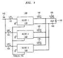
- the circuit 100 comprises a first DC/DC converter 110, a second DC/DC converter 120, and a third DC/DC converter 130 configured for parallel operation.
- the DC/DC converters 110, 120, 130 function by converting a DC input voltage to alternating current (AC) and converting the AC back into a DC output voltage.
- the DC input voltage, V in 140 is applied across the input of the circuit 100 and an input current, I in1 145, I in2 150, and I in3 155 enters the DC/DC converters 110, 120, 130, respectively.
- an output current, I out1 160, I out2 165, and I out3 170 exits each DC/DC converter 110, 120, 130, respectively.
- a combined load current, I load 180, and DC output voltage, V out 190, is delivered across an output resistive load 195.
- the normal operating mode for converters operating with forced load-sharing is for each converter to provide an equal proportion of the load current.
- the parallel pins of the converters are connected together in a star connection, which provides the necessary feedback to actively equalize the load currents.
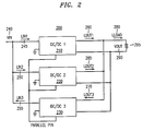
- FIGURE 2 illustrated is a schematic diagram of a plurality of synchronous rectifier converters operating in a parallel forced load-sharing synchronous rectifier converter circuit 200 with one converter processing power in a reverse direction.
- the circuit 200 comprises a first DC/DC synchronous rectifier converter 210, a second DC/DC synchronous rectifier converter 220, and a third DC/DC synchronous rectifier converter 230 configured for parallel operation.
- a voltage, V in 240 is applied across the input of the circuit 200 and an input current, I in1 245, I in2 250, enters the first and second DC/DC synchronous rectifier converters 210, 220, respectively.
- an input current, I in3 255 is illustrated exiting the third DC/DC synchronous rectifier converter 230.
- An output current, I out1 260, I out2 265, is illustrated exiting the first and second DC/DC synchronous rectifier converters 210, 220, respectively, but an output current I out3 270 enters the third DC/DC synchronous rectifier converter 230 in a reverse direction.
- a combined load current, I load 280, and output voltage, V out 290, is delivered across an output resistive load 295.
- the first and second DC/DC synchronous rectifier converters 210, 220 are processing power in a normal, forward direction, while the third DC/DC synchronous rectifier converter 230 is processing power in the reverse direction.
- the overall power system could be circulating large amounts of current while delivering very little current to the load. This results in a high power dissipation during lighter load conditions.
- FIGURE 3 illustrated is a schematic diagram of a clamped-mode forward converter circuit 300 with a synchronous rectifier circuit 330 employing the principles of the present invention.
- the clamped-mode forward converter circuit 300 and its advantages are discussed in U.S. Patent No. 5,303,138 to Rozman, issued on April 12, 1994, entitled “Low Loss Synchronous Rectifier for Application to Clamped-Mode Power Converters” and incorporated herein by reference.
- the clamped-mode forward converter circuit 300 comprises a voltage input V in 305 connected to a primary winding 310 of a power transformer by a MOSFET power switch Q1 315.
- the power switch 315 is shunted by series connection of a clamp capacitor 320 and a MOSFET switch device Q2 325.
- the conducting intervals of the power switch 315 and the switch device 325 are mutually exclusive.
- the duty cycle of the power switch 315 is D and the duty cycle of the switch device 325 is 1-D.
- a secondary winding 335 of the power transformer is connected to an output capacitance load C out 340 through an output filter inductor L out 345 and the synchronous rectifier circuit 330, providing a substantially alternating current input to the synchronous rectifier circuit 330.
- the synchronous rectifier circuit 330 comprises control circuitry 350 and switching circuitry.
- a synchronous rectifier device SR1 355 and a synchronous rectifier device SR2 360 comprise the switching circuitry.
- the switching circuitry may be realized with any suitable rectifier devices, although a low R DS(on) N-channel MOSFET is suitable for such applications.
- a diode D1 357 and a diode D2 362 are discrete devices placed in parallel with SR1 355 and SR2 360, respectively. However, D1 357 and D2 362 may represent an integral body diode of a N-channel MOSFET.
- the synchronous rectifier control circuit 350 may be either a control driven circuit, or a self-synchronized drive circuit. Additionally, the overall power train topology encompasses any topology suitable for synchronous rectification, and is not limited to the topology shown in the illustrated embodiment.
- the present invention also comprises a current sensing device 365 capable of sensing a converter output level.
- the current sensing device 365 encompasses a current transformer connected in series with Q1 315, a shunt resistor in series with the output, or a Hall effect current sense device in series with the output. The sensed current signal is then provided to the parallel control circuitry 370 to facilitate forced load-sharing.
- the current signal is also provided to a level detector 375 which compares the load current to some predetermined reference level.
- the detector 375 will disable the synchronous rectifier drive circuit 330. This action reconfigures the converter from a synchronous rectifier circuit to a conventional diode rectifier circuit. Since a diode rectifier circuit cannot process power in the reverse direction, the proposed circuit effectively prevents reverse power flow.
- the synchronous rectifier drive circuit 330 is enabled, resuming normal operation.
- the control circuit 350 transitions the switching circuitry 355, 360 from the active bidirectional mode to the inactive unidirectional mode when the output current level drops below a predetermined threshold level.
- the circuit retains the efficiency benefits of synchronous rectification at higher loads, where efficiency is most important. Reconfiguring the circuit to diode rectification at light loads prevents reverse power flow, but should not significantly impact light load efficiency. In fact, light load efficiency may be improved with diode rectification, as the overhead of the MOSFET gate drive loss is eliminated.
- the remaining circuitry is standard for synchronous rectifier circuits configured for parallel operation.
- a voltage regulator 380 monitors the load and restores the output voltage V out 342 to within tolerance limits despite changes in both the load and the input voltage V in 305.
- a pulse-width modulation (“PWM”) circuit 385 is included to keep the output voltage V out 342 of the converter constant over the various operating conditions.
- PWM pulse-width modulation
- the load current level detector circuit 375 may be disabled during non-paralleled, or stand alone, operation. An additional circuit may then be incorporated into the design that senses parallel operation (e.g. ground the parallel pin when not in use) and disable the load current level detector circuit 375 during non-parallel operation.
- FIGURE 4 illustrated is a schematic diagram of a second embodiment of the clamped-mode forward converter circuit 300 with the synchronous rectifier circuit 330 of FIGURE 3 employing the principles of the present invention.
- the clamped-mode forward converter circuit 300 is connected to the power transformer that is connected to the output capacitance load C out 340 through the output filter inductor L out 345 and the synchronous rectifier circuit 330.
- the synchronous rectifier circuit 330 comprises the switching circuitry and the control circuitry.
- the switching circuitry comprises a MOSFET rectifying device Q4 410 in parallel with a diode D1 415, and the gate of Q4 410 is coupled to a gate voltage clamping MOSFET Q6 420.
- the switching circuitry further comprises a MOSFET rectifying device Q3 425 in parallel with a diode D2 430, and the gate of Q3 425 is coupled to a gate voltage clamping MOSFET Q5 435.
- the gate voltage clamping MOSFETs and their advantages are discussed in Loftus.
- the synchronous rectifier circuit of FIGURE 4 employs a self synchronized drive circuit.
- An enabling level voltage V ctrl 440 is applied through a resistor 450 to control the proper operating voltage levels for the MOSFET rectifying devices 410, 425 and their respective drive MOSFETs 420, 435. Gate drive energy for the rectifying devices is obtained from the power train during turn on transition and returned to the power train during turn off transition.
- the control circuitry of the synchronous rectifier circuit 330 comprises a comparator 460.
- a current sensed output level from the current sensing device 365 is provided to a non-inverting input of the comparator 460 and a reference signal is provided to the inverting input of the comparator 460.
- the comparator 460 then compares the load current to the predetermined reference level. When the converter is operating below some fraction of full rated load current, perhaps 5% or 10%, the comparator 460 sends a signal to disable the synchronous rectifier drive circuit 330. This action reconfigures the converter from a synchronous rectifier circuit to a conventional diode rectifier circuit.
- the synchronous rectifier drive circuit 330 When the converter output current increases beyond the 5% or 10% trip level (some hysteresis is probably preferred), the synchronous rectifier drive circuit 330 is enabled, resuming normal operation. Thus, the control circuit 350 transitions the switching circuitry 355, 360 from the active bidirectional mode to the inactive unidirectional mode when the output current level drops below a predetermined threshold level. Therefore, the principles of the present invention are incorporated into the circuit of the illustrated embodiment.
- the proposed circuit may be necessary during "hot plug-in" of paralleled power converters.
- the output of a power converter may be energized before the converter initiates switching action.
- the MOSFETs of a self-synchronized circuit may turn on, as the gates are energized by the voltage on the output. Such a condition could lead to a catastrophic failure at "hot plug-in.”
- the synchronous MOSFETs will remain disabled until the converter starts and begins supplying output current. This possible catastrophic failure mode of self synchronized converters is therefore eliminated.
- FIGURE 5 illustrated is a timing diagram of the operation of the circuit of FIGURE 4.
- the voltage waveforms represent the voltage of the following devices.
- V ns1 510 represents the voltage at the secondary winding of the power transformer.
- V drain Q6 520 represents the drain voltage of Q6 420, and V gs Q4 530 represents the gate-to-source voltage of Q4 410.
- V drain Q5 540 represents the drain voltage of Q5 435
- V gs Q3 550 represents the gate-to-source voltage of Q3 425.
- the enable/disable signal 560 represents an enabling and disabling signal to the synchronous rectifier circuit 330.
- the circuit of FIGURE 4 operates as follows. Assume that the converter is operating at full load and that the comparator 460 (an open collector device) output is high impedance.
- the voltage V ctrl 440 (set at 10V to 12V) is a DC voltage applied to the gates of Q5 435 and Q6 420 through the resistor 450. Assume also that the converter is operating in the part of the switching cycle where Q1 315 and Q4 410 are on, and Q2 325 and Q3 425 are off. Given these initial conditions, the voltage applied to the gate of Q4 410 is clamped by Q6 420 to a threshold voltage drop (about 2V to 3V) below V ctrl 440.
- Q6 420 therefore clamps the maximum voltage applied to the gate of Q4 410, and prevents this voltage from exceeding the maximum device ratings, as shown in the V gs Q4 530 waveform.
- Q1 315 turns off and Q2 325 turns on, reversing the voltage V ns1 510 across the second winding 335.
- the gate of Q4 410 will be discharged through the body diode of Q6 (not shown), turning off Q4 410.
- Q3 425 is turned on as its gate is charged through Q5 435, and the V gs Q3 550 continues to rise until it reaches one threshold drop below V ctrl 440.
- Q1 315 turns on and Q2 325 turns off, the cycle repeats.
- the gate clamping MOSFETs, Q5 435 and Q6 420 act to limit the maximum voltage applied to the gate of the synchronous rectifier MOSFETs, Q3 425 and Q4 410, respectively. This clamping action can expand the useful input voltage range of the converter, and can also allow the use of logic level MOSFETs.
- Q5 435 and Q6 420 may be used as switches to disable the flow of channel current through Q3 425 and Q4 410.
- the comparator 460 By using the comparator 460 to ground the gates of Q5 435 and Q6 420, the synchronous MOSFETs (Q3 425 and Q4 410) can be disabled, thus reconfiguring the power train from synchronous rectification to diode rectification.
- the voltage on the non-inverting pin of the comparator 460 (the current sense signal) has a larger magnitude than the referencing voltage, which is applied to the inverting terminal of the comparator.
- the output of the comparator 460 is configured for high impedance, allowing V ctrl 440 to be applied to the gates of Q5 435 and Q6 420, resulting in normal synchronous rectifier operation.
- the current sense voltage reduces linearly.
Abstract
Description
- The present invention is directed, in general, to power conversion circuitry and, more particularly, to a control circuit for operating a power rectifier in both active bidirectional and passive unidirectional modes as a function of output level.
- Increased power density is a continuing goal of modern power supply design. High power density is particularly crucial in applications wherein the allocated space for the power supply relative to the power output is restricted. In addition to being highly compact, the power supply must also be efficient to limit heat-creating power dissipation. Illustrative applications for a high density power supply include an off-line power supply used to power a laptop computer or a power supply module for a telecommunication system employing an Integrated Services Digital Network ("ISDN").
- Bridge-type converters are particularly suitable for such applications, since they may be designed to operate resonantly. Resonance is an operational mode that permits both high power density and efficiency. One example of a bridge-type converter is a half-bridge converter as disclosed in U.S. Patent No. 5,274,543 to Loftus, issued on December 28, 1993, entitled "Zero-Voltage Switching Power Converter with Lossless Synchronous Rectifier Gate Drive" and incorporated herein by reference. Loftus' converter operates as a forward converter and includes a bridge circuit comprising two power switching transistors to drive a primary transformer.
- Loftus discloses a drive arrangement and operative scheme for driving the power transistors, thereby limiting the dissipation losses within the power switching transistors. The drive circuitry drives the power switching transistors with unequal duty cycles having a conducting duration such that the sum of the conduction intervals substantially equals the combined switching period of the power transistors. The conducting intervals are separated by very short dead time intervals controlled by the differing turn-on and turn-off times of the power switching transistor. The short interval between alternate conductions of the power switching transistors is sufficient in duration to allow zero voltage turn-on of the power switching transistors but short enough in duration to minimize power loss and conducted noise.
- Another area of concern in a power supply is an additional loss of efficiency realized through the power dissipated in the rectifier circuit of the converter. While a Schottky diode rectifier is approximately 80% efficient, a metal oxide semiconductor field effect transistor ("MOSFET") synchronous rectifier is nearly 90% efficient.
- While synchronous rectification is a relatively old concept, it has failed to gain widespread acceptance because of the unavailability of cost-effective, low RDS(on) rectifier devices (those having a small static drain-source resistance while forward-biased) . Prior practical implementations have required designers to couple many higher RDS(on) devices in parallel to arrive at a suitably low overall RDS(on). Recent advances in high cell density MOSFET technology, however, have made available MOSFET devices with very low (< 10 milliohms) RDS(on) in cost-effective, commercial packages. As a result, synchronous rectification has recently regained widespread interest; companies are beginning to introduce power converters using synchronous rectification into the marketplace.
- The normal operating mode for converters operating with forced load-sharing is for each converter to provide an equal portion of the total load current. A control terminal of the converters are coupled together in a star connection, thereby providing the necessary feedback to equalize the load currents actively.
- However, it is well known in the industry that synchronous rectifier circuits are capable of processing power bidirectionally, both from the input to the output, and from the output back to the input (of course, provided a voltage or current source externally drives the output). Bidirectional current flow can provide some significant advantages, perhaps the most common of which is elimination of the so-called critical current phenomenon found in buck-derived converters. The bidirectional current flow characteristic allows inductor current in the synchronous rectifier circuit to flow continuously, thereby avoiding a sluggish reaction to a load or transient on the output of the converter circuit.
- However, for converters connected in parallel with forced load-sharing, this bi-directional power flow characteristic can result in an undesirable (and possibly damaging) operating mode wherein one converter drives the output of another. With one or more converters operating in this reverse power processing mode, the overall power system can be circulating large amounts of current while actually delivering very little current to the load. This results in high power dissipation during lighter load conditions. Also, the system transient response could be detrimentally affected as the converters transition from the reverse power processing mode to a forward power processing mode.
- Parallel (forced load-sharing) circuitry in each converter, responsible for driving the rectifier devices, may not be able to prevent this mode of operation, as the parallel circuit is specifically designed to be effective over a limited range. See U.S. Patent No. 5,036,452 to Loftus, issued on July 30, 1991, entitled "Current Sharing Control with Limited Output Voltage Range for Paralleled Power Converters," and incorporated herein by reference, for a discussion of load sharing between power circuits connected in parallel to a common load. Therefore, it is beneficial to provide a circuit that prevents reverse power flow in converters configured for parallel operation.
- The aforementioned predicament of reverse power flow in converters for parallel operation is the subject of two articles. These articles introduce a circuit wherein the synchronous rectifier control voltage is modified to prevent reverse power flow. The circuits are generally designed either to prevent reverse power flow at converter start-up or to address "hot plug-in" problems encountered when substituting individual converters in a functioning power system.
- In the first article, "A Highly Efficient, Low-Profile 300-W Power Pack for Telecommunications Systems," APEC 1994 Proceeding, pp. 786-792, by N. Murakami, I. Yumoto, T. Yachi and K. Maki, a resonant reset forward converter with a novel synchronous rectifier drive circuit is disclosed. The circuit comprises a pair of switches to disable the gate drive of one synchronous field effect transistor ("FET") based on switch current. Another synchronous FET uses an output inductor to generate the drive voltage, and can be configured off when the inductor current goes discontinuous. The idea is to detect when the converter goes into discontinuous conduction mode, and to use this information to disable the synchronous rectifiers, thus preventing a catastrophic failure. The described circuit, which is designed for parallel operation, uses droop regulation to achieve load sharing, rather than active load sharing using a parallel pin connection. The circuit, thus, turns one of the FETs off based on switch current, and the other FET off based on a discontinuous current condition.
- While the Murakami et al. circuit attempts to solve the proposed problem it is limited for the following reasons. First, the circuit as described is only compatible with a self-synchronized drive scheme. Moreover, the circuit as described apparently only has a problem when a converter falls below critical inductor current. Both the transformer secondary voltage and the inductor voltage can collapse to zero during discontinuous conduction mode. The output voltage supplied by the paralleled modules could then energize the gates of the synchronous FETs, thus turning them on at the wrong time. Stated another way, the resonant reset topology forces a finite dead time in the gate drive of one synchronous FET, allowing the critical current point to occur. Finally, the circuit as described is limited to a passive droop sharing method, and does not accomplish active load sharing with a feedback sensing current circuit.
- In a second reference by N. Murakami, N. Yamashita and T. Yachi, entitled "A Compact, Highly Efficient 50-W On-board Power Supply Module for Telecommunications Systems," APEC 1995 Proceeding, pp. 297-302, a resonant reset forward converter with a novel synchronous rectifier drive circuit is introduced very similar to the circuit described above. The circuit comprises a pair of self synchronized FETs with a control switch in series with each gate. These switches are described as necessary to prevent reverse power flow when connected in parallel with other converters. This circuit suffers from the very same limitations inherent in the circuit described above. Again, the circuits by Murakami et al. prevent reverse power flow by turning the rectifying FET off when the voltage across the output inductor falls to zero (a condition which occurs during discontinuous inductor current mode). This prevents the bus voltage from activating the rectifying FET when the inductor voltage falls to zero. The circuits as described, however, still operate as synchronous rectifiers at all times.
- Accordingly, what is needed in the art is a control circuit for operating a power rectifier, the control circuit capable of sensing conditions under which reverse power flow may occur in the rectifier and taking steps to prevent the reverse power flow.
- To address the above-discussed deficiencies of the prior art, the present invention provides a rectifier having an input and an output and a method of controlling the rectifier. The rectifier comprises: (1) switching circuitry coupled between the input and the output, the switching circuitry adapted to operate in selected one of (a) an active bidirectional mode of operation and (b) an inactive unidirectional mode of operation to rectify substantially alternating current at the input to produce substantially direct current at the output and (2) control circuitry coupled between the rectifier output and a control input of the switching circuitry, the control circuitry capable of sensing an output level of the rectifier and transitioning the switching circuitry between the active bidirectional mode and the inactive unidirectional mode as a function of the output current level thereby to prevent substantial reverse power flow through the rectifier.
- Thus, the present invention introduces a bi-modal converter having both active and inactive (or passive) modes of operation. In the active mode, the switching circuitry switches to rectify the substantially alternating current, perhaps in resonance to realize the above-described efficiencies of a resonant converter. Bidirectional current flow is possible in the active mode. In the passive mode, the switching circuitry acts as a diode rectifier, allowing only unidirectional current and thereby preventing reverse power flow. The output level of the converter may be determined by measuring voltage, current, power or another suitable characteristic. The rectifier is particularly useful in power systems having a plurality of rectifiers operating in parallel to prevent one rectifier from driving the other.
- In a preferred embodiment of the present invention, the switching circuitry comprises MOSFET switches. Alternatively, other switches having a low RDS(on) are suitable for use with the present invention.
- In a preferred embodiment of the present invention, the rectifier is coupled in parallel with a second rectifier, the control circuitry substantially preventing the second rectifier from causing the substantial reverse power flow. Thus, the present invention is operable in a power system comprising multiple rectifiers.
- In a preferred embodiment of the present invention, the switching circuitry comprises discrete diodes to allow the switching circuitry to operate in the inactive unidirectional mode. The diodes conduct electricity when the control circuitry deactivates the active switches. As an alternative to discrete diodes, the present invention may employ body diodes integral with the MOSFET active switches.
- In a preferred embodiment of the present invention, the control circuitry comprises a sensor for detecting the output level selected from the group consisting of: (a) a current transformer in electrical communication with the output, (b) a shunt resistor coupled in series with the output and (c) a Hall effect current sense device coupled in series with the output. Those of ordinary skill in the art are familiar with other conventional current and non-current sensors and their potential applicability to the rectifier of the present invention.
- In a preferred embodiment of the present invention, the control circuit transitions the switching circuitry from the active bidirectional mode to the inactive unidirectional mode when the output level drops below a predetermined threshold level. In a more preferred embodiment, the control circuitry transitions the switching circuitry between the active bidirectional mode and the inactive unidirectional mode when the output current level is between about 5% and about 10% of a full rated output current level. Those of ordinary skill in the art will realize, however, that other output levels or ranges may be more appropriate in other applications.
- In a preferred embodiment of the present invention, the rectifier further comprises a self-synchronized drive circuit adapted to provide a drive signal to the switching circuitry for varying a duty cycle of the switching circuitry as a function of the output level (closed loop). Alternatively, the rectifier may be controlled without regard to actual output level (open loop).
- In a preferred embodiment of the present invention, the control circuitry comprises comparison circuitry for comparing the output level with a predetermined threshold level.
- In a preferred embodiment of the present invention, an active load-sharing circuit is coupled to the rectifier and a second rectifier to effect load sharing therebetween.
- In a preferred embodiment of the present invention, the control circuitry is enabled only when the rectifier is coupled in parallel with a second rectifier.
- The foregoing has outlined, rather broadly, preferred and alternative features of the present invention so that those skilled in the art may better understand the detailed description of the invention that follows. Additional features of the invention will be described hereinafter that form the subject of the claims of the invention. Those skilled in the art should appreciate that they can readily use the disclosed conception and specific embodiment as a basis for designing or modifying other structures for carrying out the same purposes of the present invention. Those skilled in the art should also realize that such equivalent constructions do not depart from the spirit and scope of the invention in its broadest form.
- For a more complete understanding of the present invention, and the advantages thereof, reference is now made to the following descriptions taken in conjunction with the accompanying drawings, in which:
- FIGURE 1 illustrates a schematic diagram of a plurality of converters operating in a parallel forced load-sharing converter circuit;
- FIGURE 2 illustrates a schematic diagram of a plurality of synchronous rectifier converters operating in a parallel forced load-sharing synchronous rectifier converter circuit with one converter processing power in a reverse direction;
- FIGURE 3 illustrates a schematic diagram of a clamped-mode forward converter circuit with a synchronous rectifier circuit employing the principles of the present invention;
- FIGURE 4 illustrates a schematic diagram of a second embodiment of the clamped-mode forward converter circuit with the synchronous rectifier circuit of FIGURE 3 employing the principles of the present invention; and
- FIGURE 5 illustrates a timing diagram of the operation of the circuit of FIGURE 4.
- Referring initially to FIGURE 1, illustrated is a schematic diagram of a plurality of converters operating in a parallel forced load-sharing
converter circuit 100. Thecircuit 100 comprises a first DC/DC converter 110, a second DC/DC converter 120, and a third DC/DC converter 130 configured for parallel operation. The DC/DC converters V in 140, is applied across the input of thecircuit 100 and an input current, Iin1 145, Iin2 150, and Iin3 155 enters the DC/DC converters DC converter V out 190, is delivered across an outputresistive load 195. The normal operating mode for converters operating with forced load-sharing is for each converter to provide an equal proportion of the load current. The parallel pins of the converters are connected together in a star connection, which provides the necessary feedback to actively equalize the load currents. - Turning now to FIGURE 2, illustrated is a schematic diagram of a plurality of synchronous rectifier converters operating in a parallel forced load-sharing synchronous
rectifier converter circuit 200 with one converter processing power in a reverse direction. Thecircuit 200 comprises a first DC/DCsynchronous rectifier converter 210, a second DC/DCsynchronous rectifier converter 220, and a third DC/DCsynchronous rectifier converter 230 configured for parallel operation. A voltage,V in 240, is applied across the input of thecircuit 200 and an input current, Iin1 245, Iin2 250, enters the first and second DC/DCsynchronous rectifier converters synchronous rectifier converter 230. An output current, Iout1 260, Iout2 265, is illustrated exiting the first and second DC/DCsynchronous rectifier converters synchronous rectifier converter 230 in a reverse direction. A combined load current, Iload 280, and output voltage,V out 290, is delivered across an outputresistive load 295. - In the illustrated embodiment, the first and second DC/DC
synchronous rectifier converters synchronous rectifier converter 230 is processing power in the reverse direction. As previously mentioned, with one or more converters operating in this reverse power processing mode, the overall power system could be circulating large amounts of current while delivering very little current to the load. This results in a high power dissipation during lighter load conditions. - Turning now to FIGURE 3, illustrated is a schematic diagram of a clamped-mode
forward converter circuit 300 with asynchronous rectifier circuit 330 employing the principles of the present invention. The clamped-modeforward converter circuit 300 and its advantages are discussed in U.S. Patent No. 5,303,138 to Rozman, issued on April 12, 1994, entitled "Low Loss Synchronous Rectifier for Application to Clamped-Mode Power Converters" and incorporated herein by reference. The clamped-modeforward converter circuit 300 comprises avoltage input V in 305 connected to a primary winding 310 of a power transformer by a MOSFETpower switch Q1 315. Thepower switch 315 is shunted by series connection of aclamp capacitor 320 and a MOSFETswitch device Q2 325. The conducting intervals of thepower switch 315 and theswitch device 325 are mutually exclusive. The duty cycle of thepower switch 315 is D and the duty cycle of theswitch device 325 is 1-D. - A secondary winding 335 of the power transformer is connected to an output
capacitance load C out 340 through an outputfilter inductor L out 345 and thesynchronous rectifier circuit 330, providing a substantially alternating current input to thesynchronous rectifier circuit 330. Thesynchronous rectifier circuit 330 comprisescontrol circuitry 350 and switching circuitry. A synchronousrectifier device SR1 355 and a synchronousrectifier device SR2 360 comprise the switching circuitry. The switching circuitry may be realized with any suitable rectifier devices, although a low RDS(on) N-channel MOSFET is suitable for such applications. Adiode D1 357 and a diode D2 362 are discrete devices placed in parallel withSR1 355 and SR2 360, respectively. However,D1 357 and D2 362 may represent an integral body diode of a N-channel MOSFET. - The synchronous
rectifier control circuit 350 may be either a control driven circuit, or a self-synchronized drive circuit. Additionally, the overall power train topology encompasses any topology suitable for synchronous rectification, and is not limited to the topology shown in the illustrated embodiment. - The present invention also comprises a
current sensing device 365 capable of sensing a converter output level. Thecurrent sensing device 365 encompasses a current transformer connected in series withQ1 315, a shunt resistor in series with the output, or a Hall effect current sense device in series with the output. The sensed current signal is then provided to theparallel control circuitry 370 to facilitate forced load-sharing. - The current signal is also provided to a
level detector 375 which compares the load current to some predetermined reference level. When the converter is operating below some fraction of full rated load current, perhaps 5% or 10%, thedetector 375 will disable the synchronousrectifier drive circuit 330. This action reconfigures the converter from a synchronous rectifier circuit to a conventional diode rectifier circuit. Since a diode rectifier circuit cannot process power in the reverse direction, the proposed circuit effectively prevents reverse power flow. When the converter output current increases beyond the 5% or 10% trip level (some hysteresis is probably preferred), the synchronousrectifier drive circuit 330 is enabled, resuming normal operation. Thus, thecontrol circuit 350 transitions the switchingcircuitry - Note that the circuit retains the efficiency benefits of synchronous rectification at higher loads, where efficiency is most important. Reconfiguring the circuit to diode rectification at light loads prevents reverse power flow, but should not significantly impact light load efficiency. In fact, light load efficiency may be improved with diode rectification, as the overhead of the MOSFET gate drive loss is eliminated.
- The remaining circuitry is standard for synchronous rectifier circuits configured for parallel operation. A
voltage regulator 380 monitors the load and restores theoutput voltage V out 342 to within tolerance limits despite changes in both the load and theinput voltage V in 305. A pulse-width modulation ("PWM")circuit 385 is included to keep theoutput voltage V out 342 of the converter constant over the various operating conditions. Finally, the circuits are coupled as illustrated by the interconnecting lines and arrows, and the synchronousrectifier control circuitry 350 and thePWM circuit 385 are coupled to the clamped-mode circuit 300 atQ1 315 andQ2 325 as illustrated. - Even though the illustrated embodiment is designed to accommodate parallel operation, in certain applications the converter could be used in a stand alone configuration. In such applications it would be desirable to retain the benefits of reverse power flow afforded by synchronous rectification, such as the elimination of critical current problems. The load current
level detector circuit 375 may be disabled during non-paralleled, or stand alone, operation. An additional circuit may then be incorporated into the design that senses parallel operation (e.g. ground the parallel pin when not in use) and disable the load currentlevel detector circuit 375 during non-parallel operation. - Turning now to FIGURE 4, illustrated is a schematic diagram of a second embodiment of the clamped-mode
forward converter circuit 300 with thesynchronous rectifier circuit 330 of FIGURE 3 employing the principles of the present invention. As discussed with respect to FIGURE 3, the clamped-modeforward converter circuit 300 is connected to the power transformer that is connected to the outputcapacitance load C out 340 through the outputfilter inductor L out 345 and thesynchronous rectifier circuit 330. Again, thesynchronous rectifier circuit 330 comprises the switching circuitry and the control circuitry. - In this illustrated embodiment, the switching circuitry comprises a MOSFET
rectifying device Q4 410 in parallel with adiode D1 415, and the gate ofQ4 410 is coupled to a gate voltage clampingMOSFET Q6 420. The switching circuitry further comprises a MOSFETrectifying device Q3 425 in parallel with adiode D2 430, and the gate ofQ3 425 is coupled to a gate voltage clampingMOSFET Q5 435. The gate voltage clamping MOSFETs and their advantages are discussed in Loftus. The synchronous rectifier circuit of FIGURE 4 employs a self synchronized drive circuit. - An enabling
level voltage V ctrl 440 is applied through aresistor 450 to control the proper operating voltage levels for theMOSFET rectifying devices respective drive MOSFETs - With continuing reference to FIGURES 3 and 4, the control circuitry of the
synchronous rectifier circuit 330 comprises acomparator 460. A current sensed output level from thecurrent sensing device 365 is provided to a non-inverting input of thecomparator 460 and a reference signal is provided to the inverting input of thecomparator 460. Thecomparator 460 then compares the load current to the predetermined reference level. When the converter is operating below some fraction of full rated load current, perhaps 5% or 10%, thecomparator 460 sends a signal to disable the synchronousrectifier drive circuit 330. This action reconfigures the converter from a synchronous rectifier circuit to a conventional diode rectifier circuit. When the converter output current increases beyond the 5% or 10% trip level (some hysteresis is probably preferred), the synchronousrectifier drive circuit 330 is enabled, resuming normal operation. Thus, thecontrol circuit 350 transitions the switchingcircuitry - Finally, the remainder of the components in the circuit with their corresponding functions are described with respect to FIGURE 4.
- The proposed circuit may be necessary during "hot plug-in" of paralleled power converters. During "hot plug-in," the output of a power converter may be energized before the converter initiates switching action. In this event, the MOSFETs of a self-synchronized circuit may turn on, as the gates are energized by the voltage on the output. Such a condition could lead to a catastrophic failure at "hot plug-in." With the proposed circuit, the synchronous MOSFETs will remain disabled until the converter starts and begins supplying output current. This possible catastrophic failure mode of self synchronized converters is therefore eliminated.
- Turning now to FIGURE 5, illustrated is a timing diagram of the operation of the circuit of FIGURE 4. The voltage waveforms represent the voltage of the following devices.
V ns1 510 represents the voltage at the secondary winding of the power transformer.V drain Q6 520 represents the drain voltage ofQ6 420, andV gs Q4 530 represents the gate-to-source voltage ofQ4 410. Comparably,V drain Q5 540 represents the drain voltage ofQ5 435, andV gs Q3 550 represents the gate-to-source voltage ofQ3 425. Finally, the enable/disablesignal 560 represents an enabling and disabling signal to thesynchronous rectifier circuit 330. - In view of the timing diagram, the circuit of FIGURE 4 operates as follows. Assume that the converter is operating at full load and that the comparator 460 (an open collector device) output is high impedance. The voltage Vctrl 440 (set at 10V to 12V) is a DC voltage applied to the gates of
Q5 435 andQ6 420 through theresistor 450. Assume also that the converter is operating in the part of the switching cycle whereQ1 315 andQ4 410 are on, andQ2 325 andQ3 425 are off. Given these initial conditions, the voltage applied to the gate ofQ4 410 is clamped byQ6 420 to a threshold voltage drop (about 2V to 3V) belowV ctrl 440.Q6 420 therefore clamps the maximum voltage applied to the gate ofQ4 410, and prevents this voltage from exceeding the maximum device ratings, as shown in theV gs Q4 530 waveform. At the end of the cycle,Q1 315 turns off andQ2 325 turns on, reversing thevoltage V ns1 510 across the second winding 335. As the voltage across the secondary winding collapses and eventually reverses, the gate ofQ4 410 will be discharged through the body diode of Q6 (not shown), turning offQ4 410.Q3 425 is turned on as its gate is charged throughQ5 435, and theV gs Q3 550 continues to rise until it reaches one threshold drop belowV ctrl 440. AsQ1 315 turns on andQ2 325 turns off, the cycle repeats. - Note that the gate clamping MOSFETs,
Q5 435 andQ6 420, act to limit the maximum voltage applied to the gate of the synchronous rectifier MOSFETs,Q3 425 andQ4 410, respectively. This clamping action can expand the useful input voltage range of the converter, and can also allow the use of logic level MOSFETs. In addition,Q5 435 andQ6 420 may be used as switches to disable the flow of channel current throughQ3 425 andQ4 410. By using thecomparator 460 to ground the gates ofQ5 435 andQ6 420, the synchronous MOSFETs (Q3 425 and Q4 410) can be disabled, thus reconfiguring the power train from synchronous rectification to diode rectification. - As previously mentioned, at higher load levels, the voltage on the non-inverting pin of the comparator 460 (the current sense signal) has a larger magnitude than the referencing voltage, which is applied to the inverting terminal of the comparator. In this condition, the output of the
comparator 460 is configured for high impedance, allowingV ctrl 440 to be applied to the gates ofQ5 435 andQ6 420, resulting in normal synchronous rectifier operation. As the load is reduced, the current sense voltage reduces linearly. At a light enough load (about 5% or 10% full load) the current sense voltage will fall below the reference, and the output of thecomparator 460 pulls the gates ofQ5 435 andQ6 420 to ground, thus disablingQ3 425 andQ4 410, respectively. The process then reverses as the load is increased. - Although the present invention has been described in detail, those skilled in the art should understand that they can make various changes, substitutions and alterations herein without departing from the spirit and scope of the invention in its broadest form.
Claims (23)
- A rectifier having an input and an output, said rectifier comprising:switching circuitry coupled between said input and said output, said switching circuitry adapted to operate in selected one of (a) an active bidirectional mode of operation and (b) an inactive unidirectional mode of operation to rectify substantially alternating current at said input to produce substantially direct current at said output; andcontrol circuitry coupled between said rectifier output and a control input of said switching circuitry, said control circuitry capable of sensing an output level of said rectifier and transitioning said switching circuitry between said active bidirectional mode and said inactive unidirectional mode as a function of said output level thereby to prevent substantial reverse power flow through said rectifier.
- The rectifier as recited in Claim 1 wherein said switching circuitry comprises metal oxide semiconductor field effect transistor (MOSFET) switches.
- The rectifier as recited in Claim 1 wherein said rectifier is coupled in parallel with a second rectifier, said control circuitry substantially preventing said second rectifier from causing said substantial reverse power flow.
- The rectifier as recited in Claim 1 wherein said switching circuitry comprises discrete diodes to allow said switching circuitry to operate in said inactive unidirectional mode.
- The rectifier as recited in Claim 1 wherein said control circuitry comprises a sensor for detecting said output level selected from the group consisting of:a current transformer in electrical communication with said output,a shunt resistor coupled in series with said output, anda Hall effect current sense device coupled in series with said output.
- The rectifier as recited in Claim 1 wherein an active load-sharing circuit is coupled to said rectifier and a second rectifier to effect load sharing therebetween.
- A method of controlling a rectifier having an input and an output, comprising the steps of:rectifying substantially alternating current at said input to produce substantially direct current at said output with switching circuitry coupled between said input and said output, said switching circuitry adapted to operate in selected one of (a) an active bidirectional mode of operation and (b) an inactive unidirectional mode of operation; andsensing an output level of said rectifier with control circuitry coupled between said rectifier output and a control input of said switching circuitry, said control circuitry capable of transitioning said switching circuitry between said active bidirectional mode and said inactive unidirectional mode as a function of said output level thereby to prevent substantial reverse power flow through said rectifier.
- The method as recited in Claim 7 wherein said switching circuitry comprises metal oxide semiconductor field effect transistor (MOSFET) switches.
- The method as recited in Claim 7 further comprising the step of coupling said rectifier in parallel with a second rectifier, said control circuitry substantially preventing said second rectifier from causing said substantial reverse power flow.
- The method as recited in Claim 7 further comprising the step of operating said switching circuitry in said inactive unidirectional mode with discrete diodes in said switching circuitry.
- The method as recited in Claim 7 wherein said step of sensing comprises the step of detecting said output level with a sensor selected from the group consisting of:a current transformer in electrical communication with said output,a shunt resistor coupled in series with said output, anda Hall effect current sense device coupled in series with said output.
- The method as recited in Claim 7 further comprising the step of transitioning said switching circuitry from said active bidirectional mode to said inactive unidirectional mode when said output level drops below a predetermined threshold level.
- The method as recited in Claim 7 further comprising the step of providing a drive signal to said switching circuitry for varying a duty cycle of said switching circuitry as a function of said output level with a self-synchronized drive circuit.
- The method as recited in Claim 7 further comprising the step of comparing said output level with a predetermined threshold level with comparison circuitry.
- The method as recited in Claim 7 further comprising the step of effecting load-sharing between said rectifier and a second rectifier with an active load-sharing circuit.
- The method as recited in Claim 7 further comprising the step of transitioning said switching circuitry between said active bidirectional mode and said inactive unidirectional mode when said output level is between about 5% and about 10% of a full rated output current level.
- The method as recited in Claim 7 further comprising the step of enabling said control circuitry only when said rectifier is coupled in parallel with a second rectifier.
- A power system having first and second rectifiers, each of said first and second rectifiers having an input and an output, each of said first and second rectifiers comprising:switching circuitry comprising a plurality of diodes and metal oxide semiconductor field effect transistor (MOSFET) switches coupled between said input and said output, said switching circuitry adapted to operate in selected one of (a) an active bidirectional mode of operation and (b) an inactive unidirectional mode of operation to rectify substantially alternating current at said input to produce substantially direct current at said output;a sensor, coupled to said output, for detecting an output level thereof;control circuitry coupled between said sensor and a control input of said switching circuitry, said control circuitry capable of transitioning said switching circuitry between said active bidirectional mode and said inactive unidirectional mode as a function of said output level thereby to prevent one of said first and second rectifiers from creating substantial reverse power flow through another of said first and second rectifiers; andan active load-sharing circuit coupled to said first and second rectifiers to effect load sharing therebetween.
- The rectifier as recited in Claim 1 or 18 wherein said control circuit transitions said switching circuitry from said active bidirectional mode to said inactive unidirectional mode when said output level drops below a predetermined threshold level.
- The rectifier as recited in Claim 1 or 18 further comprising a self-synchronized drive circuit adapted to provide a drive signal to said switching circuitry for varying a duty cycle of said switching circuitry as a function of said output level.
- The rectifier as recited in Claim 1 or 18 wherein said control circuitry comprises comparison circuitry for comparing said output level with a predetermined threshold level.
- The rectifier as recited in Claim 1 or 18 wherein said control circuitry transitions said switching circuitry between said active bidirectional mode and said inactive unidirectional mode when said output level is between about 5% and about 10% of a full rated output current level.
- The rectifier as recited in Claim 1 or 18 wherein said control circuitry is enabled only when said rectifier is coupled in parallel with a second rectifier.
Applications Claiming Priority (2)
| Application Number | Priority Date | Filing Date | Title |
|---|---|---|---|
| US43471295A | 1995-05-04 | 1995-05-04 | |
| US434712 | 1995-05-04 |
Publications (2)
| Publication Number | Publication Date |
|---|---|
| EP0741447A2 true EP0741447A2 (en) | 1996-11-06 |
| EP0741447A3 EP0741447A3 (en) | 1997-04-16 |
Family
ID=23725350
Family Applications (1)
| Application Number | Title | Priority Date | Filing Date |
|---|---|---|---|
| EP96302833A Withdrawn EP0741447A3 (en) | 1995-05-04 | 1996-04-23 | Circuit and method for controlling a synchronous recifier converter |
Country Status (2)
| Country | Link |
|---|---|
| US (4) | US5920475A (en) |
| EP (1) | EP0741447A3 (en) |
Cited By (10)
| Publication number | Priority date | Publication date | Assignee | Title |
|---|---|---|---|---|
| US5907481A (en) * | 1997-10-31 | 1999-05-25 | Telefonaktiebolaget Lm Ericsson | Double ended isolated D.C.--D.C. converter |
| EP0973246A1 (en) * | 1998-07-14 | 2000-01-19 | Lucent Technologies Inc. | Controller for a synchronous rectifier and power converter employing the same |
| WO2001003277A2 (en) * | 1999-07-07 | 2001-01-11 | Synqor, Inc. | Control of dc/dc converters having synchronous rectifiers |
| WO2001006629A1 (en) * | 1999-07-19 | 2001-01-25 | Nokia Corporation | Power source and arrangement for restricting the short-circuit current of rectifier |
| EP1195883A2 (en) | 2000-10-06 | 2002-04-10 | Salcomp OY | Control circuit for rectification |
| WO2004001937A1 (en) * | 2002-06-19 | 2003-12-31 | Sanken Electric Co., Ltd. | Sc-dc converter |
| US6894468B1 (en) | 1999-07-07 | 2005-05-17 | Synqor, Inc. | Control of DC/DC converters having synchronous rectifiers |
| US8023290B2 (en) | 1997-01-24 | 2011-09-20 | Synqor, Inc. | High efficiency power converter |
| US10199950B1 (en) | 2013-07-02 | 2019-02-05 | Vlt, Inc. | Power distribution architecture with series-connected bus converter |
| WO2021118566A1 (en) * | 2019-12-12 | 2021-06-17 | Power Integrations, Inc. | Discharge prevention of the power switch in a power converter |
Families Citing this family (206)
| Publication number | Priority date | Publication date | Assignee | Title |
|---|---|---|---|---|
| US5303138A (en) * | 1993-04-29 | 1994-04-12 | At&T Bell Laboratories | Low loss synchronous rectifier for application to clamped-mode power converters |
| US7272021B2 (en) * | 1997-01-24 | 2007-09-18 | Synqor, Inc. | Power converter with isolated and regulated stages |
| US6184660B1 (en) * | 1998-03-26 | 2001-02-06 | Micro International, Ltd. | High-side current-sensing smart battery charger |
| US6614288B1 (en) * | 1998-05-20 | 2003-09-02 | Astec International Limited | Adaptive drive circuit for zero-voltage and low-voltage switches |
| US6021059A (en) * | 1998-12-31 | 2000-02-01 | Honeywell Inc. | Integrated synchronous rectifier for power supplies |
| US6222352B1 (en) * | 1999-05-06 | 2001-04-24 | Fairchild Semiconductor Corporation | Multiple voltage output buck converter with a single inductor |
| FR2796777B1 (en) * | 1999-07-20 | 2001-09-21 | St Microelectronics Sa | CONTROL OF A POWER MOS TRANSISTOR |
| US6232754B1 (en) | 1999-08-15 | 2001-05-15 | Philips Electronics North America Corporation | Sleep-mode-ready switching power converter |
| US6191566B1 (en) * | 1999-08-26 | 2001-02-20 | Lucent Technologies Inc. | Board mountable power supply module with multi-function control pin |
| US6961253B1 (en) | 1999-10-08 | 2005-11-01 | Lambda Electronics | Drive circuits for synchronous rectifiers |
| US6442047B1 (en) * | 1999-10-08 | 2002-08-27 | Lambda Electronics, Inc. | Power conversion apparatus and methods with reduced current and voltage switching |
| US6396333B2 (en) * | 2000-01-04 | 2002-05-28 | International Rectifier Corporation | Circuit for synchronous rectification with minimal reverse recovery losses |
| US6275401B1 (en) | 2000-01-10 | 2001-08-14 | Power-One, Inc. | Self-driven synchronous rectification circuit for low output voltage DC-DC converters |
| AU2001233021A1 (en) | 2000-01-28 | 2001-08-07 | Ericsson Inc. | Simplified implementation of parallelability for modules with synchronous rectification |
| US6373732B1 (en) * | 2000-02-01 | 2002-04-16 | Compaq Information Technologies Group, L.P. | Apparatus and method for parallel synchronous power converters |
| DE60101694T2 (en) * | 2000-02-11 | 2004-12-02 | Oxford Magnet Technology Ltd., Witney | Feedback loop for power converters |
| US6351396B1 (en) * | 2000-03-04 | 2002-02-26 | Mark Elliott Jacobs | Method and apparatus for dynamically altering operation of a converter device to improve conversion efficiency |
| SE517685C2 (en) * | 2000-03-24 | 2002-07-02 | Ericsson Telefon Ab L M | Method and apparatus for controlling a synchronous rectifier in a DC converter |
| US6243278B1 (en) | 2000-04-04 | 2001-06-05 | Tyco Electronics Logistics A.G. | Drive circuit for synchronous rectifier and method of operating the same |
| US6538905B2 (en) * | 2000-04-04 | 2003-03-25 | Artesyn Technologies, Inc. | DC-to-DC power converter including at least two cascaded power conversion stages |
| US6181578B1 (en) * | 2000-04-06 | 2001-01-30 | Astec International Limited | Synchronous rectifier drive mechanism for resonant reset forward converters |
| US6301139B1 (en) | 2000-04-06 | 2001-10-09 | Power-One, Inc. | Self-driven synchronous rectifier circuit for non-optimal reset secondary voltage |
| US20010045779A1 (en) * | 2000-05-26 | 2001-11-29 | Huey Lee | Intelligent power system |
| US6218891B1 (en) | 2000-07-28 | 2001-04-17 | Lucent Technologies Inc. | Integrated circuit including a driver for a metal-semiconductor field-effect transistor |
| US6396725B1 (en) | 2000-07-31 | 2002-05-28 | Mark E. Jacobs | System and method for improving control loop response of a power supply |
| US7348760B2 (en) * | 2000-09-21 | 2008-03-25 | O2Micro International Limited | Power management topologies |
| US7564220B2 (en) * | 2000-09-21 | 2009-07-21 | O2Micro International Ltd. | Method and electronic circuit for efficient battery wake up charging |
| US6262901B1 (en) | 2000-09-29 | 2001-07-17 | Anastastios V. Simopoulos | Adjustable DC-to-DC converter with synchronous rectification and digital current sharing |
| US6400580B1 (en) | 2000-10-10 | 2002-06-04 | Wayne C. Bowman | System and method for reducing a DC magnetic flux bias in a transformer and power converter employing the same |
| US6771059B1 (en) * | 2000-11-28 | 2004-08-03 | Delta Electronics,, Inc. | Synchronous rectifier controller for power supply systems with high power switch and high efficiency |
| US6377034B1 (en) * | 2000-12-11 | 2002-04-23 | Texas Instruments Incorporated | Method and circuits for inductor current measurement in MOS switching regulators |
| US6490183B2 (en) * | 2000-12-29 | 2002-12-03 | Ericsson, Inc. | Method and apparatus for minimizing negative current build up in DC-DC converters with synchronous rectification |
| US7088602B2 (en) | 2001-01-25 | 2006-08-08 | Texas Instruments Incorporated | Active gate clamp circuit for self driven synchronous rectifiers |
| US6807073B1 (en) | 2001-05-02 | 2004-10-19 | Oltronics, Inc. | Switching type power converter circuit and method for use therein |
| US6832356B1 (en) * | 2001-05-04 | 2004-12-14 | Ixys Corporation | Gate driver for power device |
| EP1415387A4 (en) * | 2001-07-05 | 2006-08-23 | Power One Inc | Method and apparatus for controlling synchronous rectifiers of a power converter |
| US6498461B1 (en) | 2001-08-17 | 2002-12-24 | O2 Micro International Limited | Voltage mode, high accuracy battery charger |
| US7064521B2 (en) * | 2001-08-17 | 2006-06-20 | O2Micro International Limited | Charging circuit for parallel charging in multiple battery systems |
| US7202634B2 (en) * | 2001-08-17 | 2007-04-10 | O2Micro International Limited | Voltage mode, high accuracy battery charger |
| US6574124B2 (en) * | 2001-09-13 | 2003-06-03 | Netpower Technologies, Inc. | Plural power converters with individual conditioned error signals shared on a current sharing bus |
| US6760235B2 (en) * | 2001-09-13 | 2004-07-06 | Netpower Technologies, Inc. | Soft start for a synchronous rectifier in a power converter |
| JP3695379B2 (en) * | 2001-10-02 | 2005-09-14 | 日産自動車株式会社 | Power system |
| US6618274B2 (en) | 2001-10-09 | 2003-09-09 | Innoveta Technologies | Synchronous rectifier controller to eliminate reverse current flow in a DC/DC converter output |
| US6606260B2 (en) * | 2001-10-29 | 2003-08-12 | The Chamberlain Group, Inc. | Switch mode power supply for a telephone entry system or the like |
| JP3961812B2 (en) * | 2001-10-31 | 2007-08-22 | 富士通株式会社 | Power supply device and control method thereof |
| US6441597B1 (en) * | 2001-10-31 | 2002-08-27 | Semtech Corporation | Method and apparatus for sensing output inductor current in a DC-to-DC power converter |
| JP3816396B2 (en) * | 2001-12-05 | 2006-08-30 | Tdk株式会社 | Switching power supply |
| US7023710B2 (en) * | 2002-02-26 | 2006-04-04 | Koninklijke Philips Electronics N.V. | Method of operating a switched-mode power supply and switched-mode power supply |
| US6781853B2 (en) * | 2002-03-13 | 2004-08-24 | Virginia Tech Intellectual Properties, Inc. | Method and apparatus for reduction of energy loss due to body diode conduction in synchronous rectifiers |
| US6597587B1 (en) * | 2002-04-02 | 2003-07-22 | The University Of Hong Kong | Current driven synchronous rectifier with energy recovery using hysterisis driver |
| US7280026B2 (en) * | 2002-04-18 | 2007-10-09 | Coldwatt, Inc. | Extended E matrix integrated magnetics (MIM) core |
| US7118793B2 (en) * | 2002-05-22 | 2006-10-10 | Swei Mu Wang | Three-dimensional foamable structure with wear-resistant feature |
| US6873322B2 (en) | 2002-06-07 | 2005-03-29 | 02Micro International Limited | Adaptive LCD power supply circuit |
| US6756769B2 (en) | 2002-06-20 | 2004-06-29 | O2Micro International Limited | Enabling circuit for avoiding negative voltage transients |
| US6949912B2 (en) | 2002-06-20 | 2005-09-27 | 02Micro International Limited | Enabling circuit for avoiding negative voltage transients |
| JP3673245B2 (en) * | 2002-06-28 | 2005-07-20 | 株式会社東芝 | Information processing apparatus and power control method for the same |
| EP1527510A2 (en) * | 2002-07-26 | 2005-05-04 | Philips Intellectual Property & Standards GmbH | A method for controlling the transient response of a power converter powering a load, transient response controller and power converter |
| US6859020B2 (en) * | 2002-10-15 | 2005-02-22 | Texas Instruments Incorporated | Low power mode detection circuit for a DC/DC converter |
| US20040125621A1 (en) * | 2002-12-30 | 2004-07-01 | Ta-Yung Yang | Synchronous rectifier of flyback power converter |
| US6879134B2 (en) * | 2003-02-11 | 2005-04-12 | O2Micro International Limited | Selector circuit for power management in multiple battery systems |
| US6894466B2 (en) * | 2003-02-28 | 2005-05-17 | Astec International Limited | Active current sharing circuit |
| US6841977B2 (en) * | 2003-03-03 | 2005-01-11 | Astec International Limited | Soft-start with back bias conditions for PWM buck converter with synchronous rectifier |
| JP4274353B2 (en) * | 2003-03-13 | 2009-06-03 | 本田技研工業株式会社 | Bidirectional DC-DC converter |
| JP4368223B2 (en) * | 2003-03-26 | 2009-11-18 | 三洋電機株式会社 | Bias voltage generation circuit and amplifier circuit |
| JP3708090B2 (en) * | 2003-03-28 | 2005-10-19 | Tdk株式会社 | Switching power supply controller and switching power supply |
| US6853568B2 (en) * | 2003-05-20 | 2005-02-08 | Delta Electronics, Inc. | Isolated voltage regulator with one core structure |
| US20060139974A1 (en) * | 2003-06-11 | 2006-06-29 | Daniel Dermark | Power device |
| US6853562B2 (en) * | 2003-06-26 | 2005-02-08 | Optimum Power Conversion, Inc. | Voltage sense method and circuit which alleviate reverse current flow of current bi-directional converters |
| JP4064879B2 (en) * | 2003-07-02 | 2008-03-19 | 株式会社日立製作所 | Synchronous rectifier circuit and power supply device |
| US6980441B2 (en) * | 2003-07-28 | 2005-12-27 | Astec International Limited | Circuit and method for controlling a synchronous rectifier in a power converter |
| US7095638B2 (en) | 2003-09-03 | 2006-08-22 | Tyco Electronics Power Systems, Inc. | Controller for complementary switches of a power converter and method of operation thereof |
| US7199643B2 (en) * | 2003-09-26 | 2007-04-03 | Maxim Integrated Products, Inc. | Hot swappable pulse width modulation power supply circuits |
| JP4412535B2 (en) * | 2003-11-14 | 2010-02-10 | セイコーインスツル株式会社 | Synchronous rectification switching regulator control circuit and semiconductor integrated circuit including the same |
| CN100440709C (en) * | 2003-11-14 | 2008-12-03 | 力博特公司 | Variable colfficient control method for rectifier |
| US6961256B2 (en) * | 2004-02-13 | 2005-11-01 | Niko Semiconductor Co., Ltd. | Synchronous rectifier with dead time adjusting function |
| EP1754120A4 (en) * | 2004-02-19 | 2008-03-05 | Int Rectifier Corp | Dc-dc regulator with switching frequency responsive to load |
| EP1580872B1 (en) * | 2004-03-26 | 2016-05-11 | DET International Holding Limited | Control circuit |
| US7345896B2 (en) * | 2004-05-10 | 2008-03-18 | Semiconductor Components Industries, L.L.C. | Secondary side power supply controller and method therefor |
| US7002263B2 (en) * | 2004-06-09 | 2006-02-21 | Micrel, Incorporated | Elimination of recirculation current loss in load-shared switching mode power supplies |
| US7045992B1 (en) * | 2004-06-22 | 2006-05-16 | National Semiconductor Corporation | Apparatus and method for start-up for a synchronous switching regulator |
| JP4400618B2 (en) * | 2004-07-12 | 2010-01-20 | 株式会社村田製作所 | DC-DC converter |
| US7427910B2 (en) * | 2004-08-19 | 2008-09-23 | Coldwatt, Inc. | Winding structure for efficient switch-mode power converters |
| US7321283B2 (en) * | 2004-08-19 | 2008-01-22 | Coldwatt, Inc. | Vertical winding structures for planar magnetic switched-mode power converters |
| JP4434010B2 (en) * | 2004-12-28 | 2010-03-17 | サンケン電気株式会社 | DC converter |
| JP4434011B2 (en) * | 2004-12-28 | 2010-03-17 | サンケン電気株式会社 | DC converter |
| US7417875B2 (en) * | 2005-02-08 | 2008-08-26 | Coldwatt, Inc. | Power converter employing integrated magnetics with a current multiplier rectifier and method of operating the same |
| US7176662B2 (en) * | 2005-02-23 | 2007-02-13 | Coldwatt, Inc. | Power converter employing a tapped inductor and integrated magnetics and method of operating the same |
| US7385375B2 (en) * | 2005-02-23 | 2008-06-10 | Coldwatt, Inc. | Control circuit for a depletion mode switch and method of operating the same |
| US7876191B2 (en) | 2005-02-23 | 2011-01-25 | Flextronics International Usa, Inc. | Power converter employing a tapped inductor and integrated magnetics and method of operating the same |
| US7439556B2 (en) * | 2005-03-29 | 2008-10-21 | Coldwatt, Inc. | Substrate driven field-effect transistor |
| US7439557B2 (en) * | 2005-03-29 | 2008-10-21 | Coldwatt, Inc. | Semiconductor device having a lateral channel and contacts on opposing surfaces thereof |
| JP4347249B2 (en) * | 2005-03-31 | 2009-10-21 | 富士通マイクロエレクトロニクス株式会社 | DC-DC converter, control circuit for DC-DC converter, and control method for DC-DC converter |
| US7095217B1 (en) | 2005-03-31 | 2006-08-22 | O2Micro International Limited | Method circuitry and electronic device for controlling a variable output dc power source |
| US7268520B2 (en) * | 2005-04-08 | 2007-09-11 | O2Micro International Limited | Sense amplifier for use with wake-up charging current |
| US20060244429A1 (en) * | 2005-04-28 | 2006-11-02 | Astec International Limited | Free wheeling MOSFET control circuit for pre-biased loads |
| US7248979B2 (en) * | 2005-05-09 | 2007-07-24 | International Business Machines Corporation | Apparatus employing predictive failure analysis based on in-circuit FET on-resistance characteristics |
| US20060252666A1 (en) * | 2005-05-09 | 2006-11-09 | Dennis Sheirs | Household cleaning composition |
| US7339208B2 (en) * | 2005-05-13 | 2008-03-04 | Coldwatt, Inc. | Semiconductor device having multiple lateral channels and method of forming the same |
| US7675090B2 (en) * | 2005-05-13 | 2010-03-09 | Flextronics International Usa, Inc. | Semiconductor device having a contact on a buffer layer thereof and method of forming the same |
| US7405545B2 (en) * | 2005-06-08 | 2008-07-29 | System General Corp. | Voltage-regulator and power supply having current sharing circuit |
| US7511463B2 (en) * | 2005-06-21 | 2009-03-31 | Intel Corporation | Multiple output buck converter |
| CN100356675C (en) * | 2005-07-13 | 2007-12-19 | 艾默生网络能源有限公司 | Circuit for preventing restart after active hoop DC/DC inverter off |
| JP4636249B2 (en) * | 2005-07-19 | 2011-02-23 | ミツミ電機株式会社 | Current resonance type DC / DC converter and method for realizing zero current switching thereof |
| JP2007028829A (en) * | 2005-07-19 | 2007-02-01 | Mitsumi Electric Co Ltd | Current resonance dc-dc converter and its resonance current control method |
| JP2007028830A (en) * | 2005-07-19 | 2007-02-01 | Mitsumi Electric Co Ltd | Switching power supply and its control method |
| US7564074B2 (en) * | 2005-08-25 | 2009-07-21 | Flextronics International Usa, Inc. | Semiconductor device including a lateral field-effect transistor and Schottky diode |
| US7285807B2 (en) * | 2005-08-25 | 2007-10-23 | Coldwatt, Inc. | Semiconductor device having substrate-driven field-effect transistor and Schottky diode and method of forming the same |
| US7462891B2 (en) * | 2005-09-27 | 2008-12-09 | Coldwatt, Inc. | Semiconductor device having an interconnect with sloped walls and method of forming the same |
| US7568117B1 (en) * | 2005-10-03 | 2009-07-28 | Zilker Labs, Inc. | Adaptive thresholding technique for power supplies during margining events |
| US8233293B2 (en) * | 2006-01-19 | 2012-07-31 | Astec International Limited | Reverse current protection for power converters having synchronous rectifiers |
| US8595041B2 (en) * | 2006-02-07 | 2013-11-26 | Sap Ag | Task responsibility system |
| US8081493B2 (en) * | 2006-02-16 | 2011-12-20 | International Rectifier Corporation | Electronic power conditioner with integrated magnetics |
| US8415737B2 (en) | 2006-06-21 | 2013-04-09 | Flextronics International Usa, Inc. | Semiconductor device with a pillar region and method of forming the same |
| US7541640B2 (en) * | 2006-06-21 | 2009-06-02 | Flextronics International Usa, Inc. | Vertical field-effect transistor and method of forming the same |
| US7663183B2 (en) * | 2006-06-21 | 2010-02-16 | Flextronics International Usa, Inc. | Vertical field-effect transistor and method of forming the same |
| US8125205B2 (en) | 2006-08-31 | 2012-02-28 | Flextronics International Usa, Inc. | Power converter employing regulators with a coupled inductor |
| US7746042B2 (en) * | 2006-10-05 | 2010-06-29 | Advanced Analogic Technologies, Inc. | Low-noise DC/DC converter with controlled diode conduction |
| US7471072B2 (en) * | 2006-10-16 | 2008-12-30 | Semtech Corporation | Switched mode power supply having variable minimum switching frequency |
| US7675758B2 (en) * | 2006-12-01 | 2010-03-09 | Flextronics International Usa, Inc. | Power converter with an adaptive controller and method of operating the same |
| US9197132B2 (en) | 2006-12-01 | 2015-11-24 | Flextronics International Usa, Inc. | Power converter with an adaptive controller and method of operating the same |
| US7675759B2 (en) | 2006-12-01 | 2010-03-09 | Flextronics International Usa, Inc. | Power system with power converters having an adaptive controller |
| US7667986B2 (en) | 2006-12-01 | 2010-02-23 | Flextronics International Usa, Inc. | Power system with power converters having an adaptive controller |
| US7889517B2 (en) | 2006-12-01 | 2011-02-15 | Flextronics International Usa, Inc. | Power system with power converters having an adaptive controller |
| US8004111B2 (en) * | 2007-01-19 | 2011-08-23 | Astec International Limited | DC-DC switching cell modules for on-board power systems |
| US7468649B2 (en) | 2007-03-14 | 2008-12-23 | Flextronics International Usa, Inc. | Isolated power converter |
| US7741827B2 (en) * | 2007-05-01 | 2010-06-22 | Semiconductor Components Industries, Llc | Parameter control circuit including charging and discharging current mirrors and method therefor |
| US20080316779A1 (en) | 2007-06-19 | 2008-12-25 | Chandrasekaran Jayaraman | System and method for estimating input power for a power processing circuit |
| US7987928B2 (en) * | 2007-10-09 | 2011-08-02 | Pdti Holdings, Llc | Injection system and method comprising an impactor motive device |
| TWI338996B (en) * | 2007-10-16 | 2011-03-11 | Delta Electronics Inc | Resonant converter system having synchronous rectifier control circuit and controlling method thereof |
| TWM333007U (en) * | 2007-11-23 | 2008-05-21 | Power Mate Technology Co Ltd | Synchronized-rectification driving circuit |
| KR20100089820A (en) * | 2007-12-06 | 2010-08-12 | 인터실 아메리카스 인코포레이티드 | System and method for improving inductor current sensing accuracy of a dc/dc voltage regulator |
| EP2248332A4 (en) * | 2008-02-29 | 2014-03-26 | Ericsson Telefon Ab L M | Test apparatus |
| US7898831B2 (en) * | 2008-05-09 | 2011-03-01 | Alpha and Omega Semiconductor Inc. | Device and method for limiting drain-source voltage of transformer-coupled push pull power conversion circuit |
| US8154891B1 (en) | 2008-05-19 | 2012-04-10 | Raytheon Company | Methods and apparatus for selectable output DC/DC converter |
| US7911813B2 (en) * | 2008-07-21 | 2011-03-22 | System General Corp. | Offline synchronous rectifying circuit with sense transistor for resonant switching power converter |
| US7969694B2 (en) * | 2008-08-13 | 2011-06-28 | Infineon Technologies Ag | Diode loss detection for low side MOSFET of a synchronous output stage |
| KR100997397B1 (en) * | 2008-10-23 | 2010-11-30 | 주식회사 디엠비테크놀로지 | Inverter system and its operating method |
| EP2190109B1 (en) * | 2008-10-27 | 2014-09-03 | STMicroelectronics Srl | Control device for rectifiers of switching converters. |
| US8064229B2 (en) * | 2008-11-11 | 2011-11-22 | Semiconductor Components Industries, Llc | Method of forming a series resonant switching power supply control circuit and structure therefor |
| KR101030420B1 (en) | 2008-12-24 | 2011-04-20 | 삼성전기주식회사 | Switching mode power supply for reducing standby power |
| CN102342007B (en) | 2009-01-19 | 2015-01-07 | 伟创力国际美国公司 | Controller for a power converter |
| CN102342008B (en) * | 2009-01-19 | 2016-08-03 | 伟创力国际美国公司 | Controller for power converter |
| WO2010114914A1 (en) | 2009-03-31 | 2010-10-07 | Flextronics International Usa, Inc. | Magnetic device formed with u-shaped core pieces and power converter employing the same |
| JP4814975B2 (en) * | 2009-05-14 | 2011-11-16 | 三菱電機株式会社 | Power converter for vehicle |
| US8324874B2 (en) * | 2009-06-11 | 2012-12-04 | Intersil Americas Inc. | System and method for controlling synchronous switch for a synchronous converter |
| US8643222B2 (en) | 2009-06-17 | 2014-02-04 | Power Systems Technologies Ltd | Power adapter employing a power reducer |
| US8514593B2 (en) | 2009-06-17 | 2013-08-20 | Power Systems Technologies, Ltd. | Power converter employing a variable switching frequency and a magnetic device with a non-uniform gap |
| US9077248B2 (en) | 2009-06-17 | 2015-07-07 | Power Systems Technologies Ltd | Start-up circuit for a power adapter |
| US8310793B2 (en) * | 2009-07-21 | 2012-11-13 | Infineon Technologies Ag | Over-current protection for DC-to-DC converters |
| US8638578B2 (en) | 2009-08-14 | 2014-01-28 | Power System Technologies, Ltd. | Power converter including a charge pump employable in a power adapter |
| US8976549B2 (en) | 2009-12-03 | 2015-03-10 | Power Systems Technologies, Ltd. | Startup circuit including first and second Schmitt triggers and power converter employing the same |
| US8300440B2 (en) * | 2009-12-04 | 2012-10-30 | ConvenientPower HK Ltd. | AC-DC converter and AC-DC conversion method |
| US8520420B2 (en) | 2009-12-18 | 2013-08-27 | Power Systems Technologies, Ltd. | Controller for modifying dead time between switches in a power converter |
| KR20120099077A (en) * | 2009-12-28 | 2012-09-06 | 톰슨 라이센싱 | Synchronous rectifier disabling arrangement |
| US8787043B2 (en) | 2010-01-22 | 2014-07-22 | Power Systems Technologies, Ltd. | Controller for a power converter and method of operating the same |
| US9246391B2 (en) | 2010-01-22 | 2016-01-26 | Power Systems Technologies Ltd. | Controller for providing a corrected signal to a sensed peak current through a circuit element of a power converter |
| US8891268B2 (en) * | 2010-02-19 | 2014-11-18 | Texas Instruments Incorporated | System and method for soft-starting an isolated power supply system |
| CN101783594B (en) * | 2010-02-26 | 2012-05-23 | 东南大学 | Isolated high-light load efficiency low-output voltage high-current switch power source |
| WO2011116225A1 (en) | 2010-03-17 | 2011-09-22 | Power Systems Technologies, Ltd. | Control system for a power converter and method of operating the same |
| US20110239008A1 (en) * | 2010-03-26 | 2011-09-29 | Lam Kean W | Power Adapter Having a Universal Serial Bus Hub |
| ITTO20100465A1 (en) * | 2010-06-03 | 2011-12-04 | Alenia Aeronautica Spa | SWITCHING METHOD BETWEEN A LIFTING OPERATION MODE AND A VOLTAGE REDUCTION OPERATION MODE FOR A DC-DC CONVERTER |
| US8503193B2 (en) | 2010-08-26 | 2013-08-06 | Astec International Limited | Open loop DC to DC converters with enable/disable circuits |
| US8934267B2 (en) | 2010-11-09 | 2015-01-13 | Tdk-Lambda Corporation | Loosely regulated feedback control for high efficiency isolated DC-DC converters |
| US9520772B2 (en) | 2010-11-09 | 2016-12-13 | Tdk-Lambda Corporation | Multi-level voltage regulator system |
| US8723492B2 (en) | 2011-03-22 | 2014-05-13 | Integrated Device Technology, Inc. | Autonomous controlled headroom low dropout regulator for single inductor multiple output power supply |
| US8792257B2 (en) | 2011-03-25 | 2014-07-29 | Power Systems Technologies, Ltd. | Power converter with reduced power dissipation |
| US9054593B2 (en) * | 2011-06-02 | 2015-06-09 | Hewlett-Packard Development Company, L.P. | Impedance control for a power converter |
| US8737099B2 (en) * | 2011-07-15 | 2014-05-27 | O2Micro, Inc. | Controllers for power converters |
| US9397579B2 (en) | 2011-07-15 | 2016-07-19 | O2Micro Inc | Full-bridge switching DC/DC converters and controllers thereof |
| JP5771090B2 (en) * | 2011-07-27 | 2015-08-26 | エヌ・ティ・ティ・データ先端技術株式会社 | Power supply system |
| LT2745372T (en) * | 2011-08-17 | 2020-04-10 | Belenos Clean Power Holding Ag | Dc/dc converter for hybrid system |
| US9906147B2 (en) * | 2011-09-14 | 2018-02-27 | Futurewei Technologies, Inc. | Adaptive dead time control apparatus and method for switching power converters |
| US9154045B2 (en) * | 2011-10-07 | 2015-10-06 | Raytheon Company | Distributed power conditioning with DC-DC converters implemented in heterogeneous integrated circuit |
| US8792256B2 (en) | 2012-01-27 | 2014-07-29 | Power Systems Technologies Ltd. | Controller for a switch and method of operating the same |
| KR101345780B1 (en) | 2012-05-25 | 2014-01-02 | 주식회사 대윤정보통신 | a Hybrid Converter using a inductor |
| TWI540822B (en) * | 2012-07-03 | 2016-07-01 | 盈正豫順電子股份有限公司 | Control method for bidirectional dc/dc converters |
| US9190898B2 (en) | 2012-07-06 | 2015-11-17 | Power Systems Technologies, Ltd | Controller for a power converter and method of operating the same |
| US9379629B2 (en) | 2012-07-16 | 2016-06-28 | Power Systems Technologies, Ltd. | Magnetic device and power converter employing the same |
| US9099232B2 (en) | 2012-07-16 | 2015-08-04 | Power Systems Technologies Ltd. | Magnetic device and power converter employing the same |
| US9214264B2 (en) | 2012-07-16 | 2015-12-15 | Power Systems Technologies, Ltd. | Magnetic device and power converter employing the same |
| US9106130B2 (en) | 2012-07-16 | 2015-08-11 | Power Systems Technologies, Inc. | Magnetic device and power converter employing the same |
| US8922255B1 (en) * | 2013-07-17 | 2014-12-30 | Texas Instruments Incorporated | PWM controller with drive signal on current sensing pin |
| US20150180343A1 (en) * | 2012-07-27 | 2015-06-25 | Telefonaktiebolaget L M Ericsson (Publ) | Control of a synchronous rectifier |
| US9240712B2 (en) | 2012-12-13 | 2016-01-19 | Power Systems Technologies Ltd. | Controller including a common current-sense device for power switches of a power converter |
| CN103248251B (en) * | 2013-05-17 | 2016-06-08 | 成都英格瑞德电气有限公司 | Automatic variable coefficient control method for inverter |
| JP6188487B2 (en) * | 2013-08-26 | 2017-08-30 | ローム株式会社 | DC / DC converter, operation method thereof, and electronic apparatus |
| US9300206B2 (en) | 2013-11-15 | 2016-03-29 | Power Systems Technologies Ltd. | Method for estimating power of a power converter |
| US20150194900A1 (en) * | 2014-01-06 | 2015-07-09 | Bel Fuse (Macao Commercial Offshore) Limited | Power converter with modulated secondary-side synchronous rectification |
| JP2015149815A (en) * | 2014-02-05 | 2015-08-20 | 株式会社デンソー | power converter |
| US9831768B2 (en) | 2014-07-17 | 2017-11-28 | Crane Electronics, Inc. | Dynamic maneuvering configuration for multiple control modes in a unified servo system |
| US20170025969A1 (en) * | 2015-07-22 | 2017-01-26 | Texas Instruments Incorporated | Synchronous rectifier phase control to improve load efficiency |
| CN108880249A (en) * | 2015-08-25 | 2018-11-23 | 华为技术有限公司 | Voltage conversion circuit, method and Multiphase Parallel power-supply system |
| JP6484529B2 (en) * | 2015-08-26 | 2019-03-13 | コーセル株式会社 | Switching power supply |
| DE102015224858A1 (en) * | 2015-12-10 | 2017-06-14 | Robert Bosch Gmbh | Method and device for controlling a galvanically isolated DC-DC converter |
| US10050555B2 (en) * | 2016-03-18 | 2018-08-14 | Vertiv Energy Systems, Inc. | Power supplies having synchronous and asynchronous modes of operation |
| US9780635B1 (en) | 2016-06-10 | 2017-10-03 | Crane Electronics, Inc. | Dynamic sharing average current mode control for active-reset and self-driven synchronous rectification for power converters |
| DE102016220201A1 (en) * | 2016-10-17 | 2018-04-19 | Continental Automotive Gmbh | DC-DC converter with active backflow barrier and method for operating a DC-DC converter |
| US10554138B2 (en) | 2016-10-25 | 2020-02-04 | Infineon Technologies Austria Ag | Flux limited fast transient response in isolated DC-DC converters |
| US9742183B1 (en) | 2016-12-09 | 2017-08-22 | Crane Electronics, Inc. | Proactively operational over-voltage protection circuit |
| US9735566B1 (en) | 2016-12-12 | 2017-08-15 | Crane Electronics, Inc. | Proactively operational over-voltage protection circuit |
| CN108233708B (en) * | 2016-12-14 | 2020-12-29 | 中国航空工业集团公司西安航空计算技术研究所 | Wide-range input airborne DCDC auxiliary power supply circuit |
| US10439500B2 (en) * | 2017-02-01 | 2019-10-08 | Infineon Technologies Austria Ag | Control of isolated power converters during transient load conditions |
| US10270347B2 (en) | 2017-08-18 | 2019-04-23 | Honeywell International Inc. | Short-circuit protected power supply circuit |
| US9979285B1 (en) | 2017-10-17 | 2018-05-22 | Crane Electronics, Inc. | Radiation tolerant, analog latch peak current mode control for power converters |
| US10425080B1 (en) | 2018-11-06 | 2019-09-24 | Crane Electronics, Inc. | Magnetic peak current mode control for radiation tolerant active driven synchronous power converters |
| US10797608B2 (en) * | 2019-02-14 | 2020-10-06 | Dialog Semiconductor Inc. | Flyback converter with edge-based isolated communication |
Citations (1)
| Publication number | Priority date | Publication date | Assignee | Title |
|---|---|---|---|---|
| WO1995002918A1 (en) * | 1993-07-14 | 1995-01-26 | Melcher Ag | Synchronous rectifier resistant to feedback |
Family Cites Families (22)
| Publication number | Priority date | Publication date | Assignee | Title |
|---|---|---|---|---|
| US4371919A (en) * | 1981-04-29 | 1983-02-01 | Bell Telephone Laboratories, Incorporated | Load distribution among parallel DC-DC converters |
| US4716514A (en) * | 1984-12-13 | 1987-12-29 | Unitrode Corporation | Synchronous power rectifier |
| US4870555A (en) * | 1988-10-14 | 1989-09-26 | Compaq Computer Corporation | High-efficiency DC-to-DC power supply with synchronous rectification |
| US4922404A (en) * | 1989-03-15 | 1990-05-01 | General Electric Company | Method and apparatus for gating of synchronous rectifier |
| DE3914799A1 (en) * | 1989-05-05 | 1990-11-08 | Standard Elektrik Lorenz Ag | FLOW CONVERTER |
| US5036452A (en) * | 1989-12-28 | 1991-07-30 | At&T Bell Laboratories | Current sharing control with limited output voltage range for paralleled power converters |
| US5038266A (en) * | 1990-01-02 | 1991-08-06 | General Electric Company | High efficiency, regulated DC supply |
| FR2663169A1 (en) * | 1990-06-08 | 1991-12-13 | Alcatel Espace | DEVICE FOR REGULATING A PARAMETER BY A BIDIRECTIONAL CURRENT STRUCTURE. |
| JP2682202B2 (en) * | 1990-06-08 | 1997-11-26 | 日本電気株式会社 | Rectifier circuit using field effect transistor |
| JP2592751Y2 (en) * | 1990-11-26 | 1999-03-24 | 日本電気株式会社 | Power panel equipment |
| US5179512A (en) * | 1991-09-18 | 1993-01-12 | General Electric Company | Gate drive for synchronous rectifiers in resonant converters |
| US5255174A (en) * | 1991-10-18 | 1993-10-19 | Allied-Signal Inc. | Regulated bi-directional DC-to-DC voltage converter which maintains a continuous input current during step-up conversion |
| US5274543A (en) * | 1992-04-20 | 1993-12-28 | At&T Bell Laboratories | Zero-voltage switching power converter with lossless synchronous rectifier gate drive |
| US5430640A (en) * | 1992-04-30 | 1995-07-04 | Samsung Electro-Mechanics Co., Ltd. | Power supply |
| US5396412A (en) * | 1992-08-27 | 1995-03-07 | Alliedsignal Inc. | Synchronous rectification and adjustment of regulator output voltage |
| JPH06133550A (en) * | 1992-10-12 | 1994-05-13 | Nemitsuku Ramuda Kk | Power supply |
| US5282123A (en) * | 1992-12-16 | 1994-01-25 | At&T Bell Laboratories | Clamped mode DC-DC converter |
| US5625541A (en) * | 1993-04-29 | 1997-04-29 | Lucent Technologies Inc. | Low loss synchronous rectifier for application to clamped-mode power converters |
| US5303138A (en) * | 1993-04-29 | 1994-04-12 | At&T Bell Laboratories | Low loss synchronous rectifier for application to clamped-mode power converters |
| JPH06319255A (en) * | 1993-04-30 | 1994-11-15 | Fujitsu Ltd | Dc converter |
| US5528480A (en) * | 1994-04-28 | 1996-06-18 | Elonex Technologies, Inc. | Highly efficient rectifying and converting circuit for computer power supplies |
| US5457624A (en) * | 1994-06-13 | 1995-10-10 | Texas Instruments Incorporated | Efficient switched mode power converter circuit and method |
-
1996
- 1996-04-23 EP EP96302833A patent/EP0741447A3/en not_active Withdrawn
- 1996-08-14 US US08/696,674 patent/US5920475A/en not_active Expired - Lifetime
-
1997
- 1997-07-02 US US08/887,502 patent/US5956245A/en not_active Expired - Lifetime
-
1999
- 1999-07-02 US US09/346,848 patent/US6038154A/en not_active Expired - Lifetime
- 1999-12-27 US US09/472,617 patent/US6191964B1/en not_active Expired - Lifetime
Patent Citations (1)
| Publication number | Priority date | Publication date | Assignee | Title |
|---|---|---|---|---|
| WO1995002918A1 (en) * | 1993-07-14 | 1995-01-26 | Melcher Ag | Synchronous rectifier resistant to feedback |
Cited By (19)
| Publication number | Priority date | Publication date | Assignee | Title |
|---|---|---|---|---|
| US8023290B2 (en) | 1997-01-24 | 2011-09-20 | Synqor, Inc. | High efficiency power converter |
| US9143042B2 (en) | 1997-01-24 | 2015-09-22 | Synqor, Inc. | High efficiency power converter |
| US8493751B2 (en) | 1997-01-24 | 2013-07-23 | Synqor, Inc. | High efficiency power converter |
| US5907481A (en) * | 1997-10-31 | 1999-05-25 | Telefonaktiebolaget Lm Ericsson | Double ended isolated D.C.--D.C. converter |
| EP0973246A1 (en) * | 1998-07-14 | 2000-01-19 | Lucent Technologies Inc. | Controller for a synchronous rectifier and power converter employing the same |
| WO2001003277A3 (en) * | 1999-07-07 | 2001-11-01 | Synqor Inc | Control of dc/dc converters having synchronous rectifiers |
| US6894468B1 (en) | 1999-07-07 | 2005-05-17 | Synqor, Inc. | Control of DC/DC converters having synchronous rectifiers |
| WO2001003277A2 (en) * | 1999-07-07 | 2001-01-11 | Synqor, Inc. | Control of dc/dc converters having synchronous rectifiers |
| US7119524B2 (en) | 1999-07-07 | 2006-10-10 | Bank America, N.A. | Control of DC/DC converters having synchronous rectifiers |
| WO2001006629A1 (en) * | 1999-07-19 | 2001-01-25 | Nokia Corporation | Power source and arrangement for restricting the short-circuit current of rectifier |
| US6671193B1 (en) | 1999-07-19 | 2003-12-30 | Nokia Corporation | Power source and arrangement for restricting the short-circuit current or rectifier |
| EP1195883A3 (en) * | 2000-10-06 | 2004-09-29 | Salcomp OY | Control circuit for rectification |
| EP1195883A2 (en) | 2000-10-06 | 2002-04-10 | Salcomp OY | Control circuit for rectification |
| WO2004001937A1 (en) * | 2002-06-19 | 2003-12-31 | Sanken Electric Co., Ltd. | Sc-dc converter |
| US10199950B1 (en) | 2013-07-02 | 2019-02-05 | Vlt, Inc. | Power distribution architecture with series-connected bus converter |
| US10594223B1 (en) | 2013-07-02 | 2020-03-17 | Vlt, Inc. | Power distribution architecture with series-connected bus converter |
| US11075583B1 (en) | 2013-07-02 | 2021-07-27 | Vicor Corporation | Power distribution architecture with series-connected bus converter |
| US11705820B2 (en) | 2013-07-02 | 2023-07-18 | Vicor Corporation | Power distribution architecture with series-connected bus converter |
| WO2021118566A1 (en) * | 2019-12-12 | 2021-06-17 | Power Integrations, Inc. | Discharge prevention of the power switch in a power converter |
Also Published As
| Publication number | Publication date |
|---|---|
| US6038154A (en) | 2000-03-14 |
| US6191964B1 (en) | 2001-02-20 |
| US5956245A (en) | 1999-09-21 |
| EP0741447A3 (en) | 1997-04-16 |
| US5920475A (en) | 1999-07-06 |
Similar Documents
| Publication | Publication Date | Title |
|---|---|---|
| US5956245A (en) | Circuit and method for controlling a synchronous rectifier converter | |
| US6618274B2 (en) | Synchronous rectifier controller to eliminate reverse current flow in a DC/DC converter output | |
| US5471376A (en) | Low-loss active voltage-clamp circuit for single-ended forward PWM converter | |
| EP1236265B8 (en) | Externally-driven scheme for synchronous rectification | |
| US7558082B2 (en) | Method and apparatus for controlling a synchronous rectifier | |
| US7345896B2 (en) | Secondary side power supply controller and method therefor | |
| US6426884B1 (en) | Reducing reverse currents in a synchronous rectifier circuit | |
| CN101632216B (en) | Clamp diode reset in a power converter and power outage detection in a switched mode power supply | |
| US6058026A (en) | Multiple output converter having a single transformer winding and independent output regulation | |
| US5581454A (en) | High power switched capacitor voltage conversion and regulation apparatus | |
| JP4574930B2 (en) | Resonant gate driver for synchronous rectifier | |
| US20060262575A1 (en) | Power converter with isolated and regulation stages | |
| JP3510178B2 (en) | DC power supply and control circuit thereof | |
| US5307005A (en) | Zero current switching reverse recovery circuit | |
| EP0957568B1 (en) | Current resonance type switching power source | |
| US6459600B2 (en) | Method of connecting synchronous rectifier modules in parallel without output voltage faults | |
| US5293111A (en) | Method for minimizing the switching loss in a power switch | |
| WO2006095327A2 (en) | Switched mode power converter and method of operation thereof | |
| US20110149616A1 (en) | Drive circuit for a synchronous rectifier and a method for controlling it | |
| EP1229635B1 (en) | Active gate clamp circuit for self driven synchronous rectifiers | |
| JP3202416B2 (en) | Synchronous rectifier converter | |
| US6262905B1 (en) | Secondary-side controlled resonant AC voltage regulator module | |
| JP3341825B2 (en) | Synchronous rectification type DC-DC converter | |
| US6696772B2 (en) | Synchronous rectification | |
| EP1104084A2 (en) | Efficient parallel connection of improved power-supplies |
Legal Events
| Date | Code | Title | Description |
|---|---|---|---|
| PUAI | Public reference made under article 153(3) epc to a published international application that has entered the european phase |
Free format text: ORIGINAL CODE: 0009012 |
|
| AK | Designated contracting states |
Kind code of ref document: A2 Designated state(s): DE FR GB IT |
|
| PUAL | Search report despatched |
Free format text: ORIGINAL CODE: 0009013 |
|
| AK | Designated contracting states |
Kind code of ref document: A3 Designated state(s): DE FR GB IT |
|
| 17P | Request for examination filed |
Effective date: 19971003 |
|
| 17Q | First examination report despatched |
Effective date: 19980930 |
|
| APAB | Appeal dossier modified |
Free format text: ORIGINAL CODE: EPIDOS NOAPE |
|
| APAB | Appeal dossier modified |
Free format text: ORIGINAL CODE: EPIDOS NOAPE |
|
| APBJ | Interlocutory revision of appeal recorded |
Free format text: ORIGINAL CODE: EPIDOS IRAPE |
|
| STAA | Information on the status of an ep patent application or granted ep patent |
Free format text: STATUS: THE APPLICATION IS DEEMED TO BE WITHDRAWN |
|
| 18D | Application deemed to be withdrawn |
Effective date: 20010821 |