EP0715178A2 - Integrated circuit comprising a testing pad - Google Patents
Integrated circuit comprising a testing pad Download PDFInfo
- Publication number
- EP0715178A2 EP0715178A2 EP95118691A EP95118691A EP0715178A2 EP 0715178 A2 EP0715178 A2 EP 0715178A2 EP 95118691 A EP95118691 A EP 95118691A EP 95118691 A EP95118691 A EP 95118691A EP 0715178 A2 EP0715178 A2 EP 0715178A2
- Authority
- EP
- European Patent Office
- Prior art keywords
- circuit
- integrated circuit
- module
- section
- testing
- Prior art date
- Legal status (The legal status is an assumption and is not a legal conclusion. Google has not performed a legal analysis and makes no representation as to the accuracy of the status listed.)
- Granted
Links
Images

Classifications
-
- H—ELECTRICITY
- H01—ELECTRIC ELEMENTS
- H01L—SEMICONDUCTOR DEVICES NOT COVERED BY CLASS H10
- H01L22/00—Testing or measuring during manufacture or treatment; Reliability measurements, i.e. testing of parts without further processing to modify the parts as such; Structural arrangements therefor
-
- G—PHYSICS
- G01—MEASURING; TESTING
- G01R—MEASURING ELECTRIC VARIABLES; MEASURING MAGNETIC VARIABLES
- G01R31/00—Arrangements for testing electric properties; Arrangements for locating electric faults; Arrangements for electrical testing characterised by what is being tested not provided for elsewhere
- G01R31/28—Testing of electronic circuits, e.g. by signal tracer
- G01R31/317—Testing of digital circuits
- G01R31/31712—Input or output aspects
- G01R31/31715—Testing of input or output circuits; test of circuitry between the I/C pins and the functional core, e.g. testing of input or output driver, receiver, buffer
-
- G—PHYSICS
- G01—MEASURING; TESTING
- G01R—MEASURING ELECTRIC VARIABLES; MEASURING MAGNETIC VARIABLES
- G01R31/00—Arrangements for testing electric properties; Arrangements for locating electric faults; Arrangements for electrical testing characterised by what is being tested not provided for elsewhere
- G01R31/28—Testing of electronic circuits, e.g. by signal tracer
- G01R31/317—Testing of digital circuits
- G01R31/31712—Input or output aspects
-
- G—PHYSICS
- G01—MEASURING; TESTING
- G01R—MEASURING ELECTRIC VARIABLES; MEASURING MAGNETIC VARIABLES
- G01R31/00—Arrangements for testing electric properties; Arrangements for locating electric faults; Arrangements for electrical testing characterised by what is being tested not provided for elsewhere
- G01R31/28—Testing of electronic circuits, e.g. by signal tracer
- G01R31/317—Testing of digital circuits
- G01R31/3181—Functional testing
- G01R31/3185—Reconfiguring for testing, e.g. LSSD, partitioning
- G01R31/318505—Test of Modular systems, e.g. Wafers, MCM's
-
- G—PHYSICS
- G02—OPTICS
- G02B—OPTICAL ELEMENTS, SYSTEMS OR APPARATUS
- G02B26/00—Optical devices or arrangements for the control of light using movable or deformable optical elements
- G02B26/08—Optical devices or arrangements for the control of light using movable or deformable optical elements for controlling the direction of light
- G02B26/0816—Optical devices or arrangements for the control of light using movable or deformable optical elements for controlling the direction of light by means of one or more reflecting elements
- G02B26/0833—Optical devices or arrangements for the control of light using movable or deformable optical elements for controlling the direction of light by means of one or more reflecting elements the reflecting element being a micromechanical device, e.g. a MEMS mirror, DMD
- G02B26/0841—Optical devices or arrangements for the control of light using movable or deformable optical elements for controlling the direction of light by means of one or more reflecting elements the reflecting element being a micromechanical device, e.g. a MEMS mirror, DMD the reflecting element being moved or deformed by electrostatic means
-
- G—PHYSICS
- G06—COMPUTING; CALCULATING OR COUNTING
- G06F—ELECTRIC DIGITAL DATA PROCESSING
- G06F11/00—Error detection; Error correction; Monitoring
- G06F11/22—Detection or location of defective computer hardware by testing during standby operation or during idle time, e.g. start-up testing
- G06F11/26—Functional testing
- G06F11/273—Tester hardware, i.e. output processing circuits
- G06F11/2733—Test interface between tester and unit under test
Definitions
- the present invention is generally related to the fabrication and design of large integrated circuits, and more particularly, to the design and testing of large integrated circuits having a die which is too impractical to test with commercially available automated die probers.
- semiconductor dies Since the invention of the integrated circuit, semiconductor dies have become increasingly more sophisticated and large in size. To ensure providing high quality and reliable products to industry, semiconductor manufactururers traditionally functionally test and optically inspect their integrated circuits before the die is packaged.
- SLM Spatial Light Modulator
- DMD Digital Micromirror Devices
- SLM Spatial Light Modulator
- DMDs can be implemented in both hard copy electrostatic printers, and can also be used to provide high resolution displays including monitors and large screen televisions.
- DMDs implemented in the design of a television are disclosed is U.S. Patent 5,079,544, to DeMond et al. entitled Standard Independent Digitized Video System and Published European Patent document 0,332,953, both assigned to the assignee of the present invention.
- a DMD incorporated into a hard copy printing device is disclosed in Published European Patent document 0,433,981 also assigned to the assignee of the present invention.
- DMDs for the hard copy printing products are especially challenging due to the fact that the integrated circuits are approaching 5 inches in length.
- These DMDs comprise a linear array of micromirrors serving as pixels, and may comprise an array of 64 by 7,056 pixels.
- One invention which addresses the need to reliably manufacture large integrated circuits of this magnitude is disclosed in the cross referenced patent application, wherein a single reticle is implemented in a step and repeat procedure using conventional photolithography equipment. By implementing a single reticle, the step and repeat procedure exposes the die one module at a time, wherein some intermediate modules are repeated, to reliably align one module with an adjacent module. With this design technique available to fabricate large integrated circuits of enormous sizes, the forgoing invention sets out to provide the testability of an integrated circuit of this size and sophistication.
- the present invention finds technical advantages by providing a large integrated circuit comprised of several interconnected circuit modules each with a dedicated testing pad structure.
- the modular integrated circuit is such that it can be tested one module at a time by a conventional prober, with each module tested as an independent integrated circuit.
- the probe pads provided for testing the associated circuit of the module are consistently arranged and located module-to-module such that they can be accessed by the automated prober which steps from module to module.
- each module comprising the elongated integrated circuit has testing pads which can be used to test the circuity on that associated module.
- the testing pads can also be used to control testing of the entire integrated circuit, including circuitry of other modules comprising that integrated circuit.
- Some circuit modules are also provided with controllable gate circuits to allow selective access by other modules. When the testing step is not implemented, such as during normal operation of the integrated circuit, these testing pads are functionally and electrically isolated by the gate circuits from the rest of the integrated circuit so as not to interfere with normal operation of the circuit.
- each circuit module can be tested, individually, even though it may require providing signals to adjacent modules.
- each circuit module comprising the integrated circuit with dedicated testing pads, some pads permitting control of the entire integrated circuit, failure analysis is both possible and practical. Moreover, since the testing pads can later be electrically isolated from the rest of the functional circuitry, these testing pads do not degrade the performance of the integrated circuit during normal operation.
- the present invention will be set forth as implemented in a DMD die used in a hard copy device manufactured by Texas Instruments Incorporated of Dallas Texas.
- This hard copy device implements a DMD type SLM comprising a modular integrated circuit of approximately 5 inches in length.
- the DMD hard copy product is set forth in Published European Patent document 0,433,981.
- FIG. 1 a simplified block diagram of an elongated integrated circuit for use in the hard copy product is shown.
- the integrated circuit is generally shown at 10 and is seen to comprise a left control circuit module 12, a right control circuit module 14, and a plurality of identical intermediate circuit modules 16. These modules are shown to be interconnected and arranged adjacent to one another and forming a linear array of pixels which may be of the size of 64 by 7,056 pixels. Each of circuit modules 12 and 14 may also have pixels, as shown, which form a portion of the overall pixel array.
- This elongated integrated circuit 10 may be fabricated using the unique process disclosed in Published European Patent document 0,602,634 assigned to the assignee of the present invention.
- the elongated 5 inch die is fabricated using a single reticle to step and repeat across a wafer using conventional photolithography techniques. Since each of the intermediate circuit modules 16 forming the mirror array are identical with one another, only three patterns are required of this reticle to expose and fabricate the large elongated integrated circuit as shown in Figure 1. Each of circuit modules 12, 14 and 16 are shown to electrically interface on at least one side with an adjacent circuit module via connections which are precisionally achieved using this novel step and repeat process.
- each of circuit modules 12, 14 and 16 are also each seen to include a group of testing pads generally shown at 20.
- Each of these testing pads is electrically connected to one conductor of the associated circuitry on that particular module.
- the associated circuitry on each module may be functionally exercised, while being subjected to conditions including vibration, humidity and extreme temperatures if desired.
- the testing pads sections 20 of each module are provided in identical locations relative to the module such that standard prober equipment (not shown) can be easily stepped across the circuit 10 from one module to the next during the testing procedure.
- the pads for each section 20 are identically laid out, and are preferably commonly identified from module to module, as shown. For instance, the left most pad may be identified as the "T" pad of each testing pad section 20.
- the second, third etc. testing pad as viewed left to right, would also be identically labeled for each testing pad as 20 section as shown. However, each of these testing pads could be used and identified differently from module to module if desired, depending on the circuitry and requirements of the associated module or the overall circuit 10.
- a left logic circuit section 22 and a right logic circuit 24 can be seen to each be electrically coupled to respective testing pads D1 and D2.
- a gate or switching circuit 26 is seen to also be provided on each circuit module 12 and 14.
- the left gate circuit 26 of module 12 permits pads L1 and L2 of all modules to be selectively electrically connected to left logic circuit 22, and the right gate circuit 26 of module 14 permits all pads R1 and R2 to be selectively electrically connected to right logic circuit 24.
- Each testing pad "T" is seen to be connected to these gate circuits 26 via line 28, and are used to selectively enable these gate sections 26.
- Each of intermediate circuit modules 16 can be seen to have array of pixels represented at 34, such as deflectable micro mirrors which are normally addressed and controlled by the logic circuitry 22 of module 12, as well as the logic circuit 24 provided on the right circuit module 14.
- the control of this array is via lines 36, as shown, which represent row and column address lines, clock lines, read and write lines, etc.
- circuit conductors 30, 32, 38, and 40 are provided to selectively connect each of testing pads L1, L2, R1 and R2 to the appropriate logic circuits 22 and 24, via the respective gating circuitry 26, as shown.
- a conventional prober (not shown) can access each testing pad section 20 in a well known manner, and functionally exercise respective array 34. Power and ground is provided to integrated circuit 10 via any of testing pads P and G.
- Gate circuitry 26 comprises a separate MOS transistor switching device 50 in series with each associated signal line, such as lines 30, 32, 38 and 40 as shown in Figure 1.
- Each MOS transistor 50 has its drain terminal connected to the input side, and its source terminal connected to the output side.
- the gate terminal of each MOS transistor 50 is connected to the test enable line 28, this test enable line being connected to pad "T" of each pad section 20 of Figure 1. By enabling test line 28, each switching transistor 50 will be caused to conduct allowing respective signals to pass therethrough from the drain terminal to the source terminal.
- testing line 28 is grounded on line 42 by a system controller (not shown), thereby causing transistors 50 to turn off and disconnect the input line from the respective output line. Therefore, during normal operation of integrated circuit 10, the testing pads 20 can be disconnected from the outside lines connecting the system controller to logic circuits 22 and 34, shown at 44, 46, 48 and 50, thereby avoiding any RC problems.
- the test enable line 28 is inverted by a pair of inverters 52. The output of each inverter 52 is connected to the gate terminal of a respective MOS transistor 54. Grounding pad "T" turns MOS transistors 54 on. Each transistor 54 has its drain terminal grounded, and its source terminal connected to the respective input line 30 or 32. Therefore, when the testing function is disabled by grounding line 28, transistors 54 in turn ground the input lines 30 and 32 to avoid floating.
- each integrated circuit module 12, 14 and 16 will be individually tested using a conventional off the shelf testing prober (not shown), such as one of those manufactured by the Hewlett Packard Corporation, and Teledyne Corporation.
- the prober equipment is coupled to the appropriate pads of pad section 20 of circuit module 12, and power and ground is applied to the P and G pads of respective section 20.
- an enable signal such as +5 volts, is applied to test enable pad "T", thereby enabling each of gate sections 26 on circuit modules 12 and 14.
- testing signals are applied to testing pads L1, L2, D1, D2, R1 and R2 to appropriately test and exercise the associated circuitry 22.
- circuit module 12 has been tested using a software routine which may be custom designed for this associated circuit module 12, the prober equipment is stepped right to the next circuit module 16 to be tested, and connected to the testing pad section 20 with associated module circuitry 34.
- Test enable pad T is biased, and appropriate testing signals are provided to the testing pads 20 to functionally exercise the respective array circuitry 34 of the associated circuit module 16. While some testing signals are unswitched and provided directly to array 34 via respective testing pads D1 and D2 such as clock signals, other testing circuit signals needed to operate array 34 such as row and column address bits, write and read bits, etc., are provided to the left and right logic circuitry 22 and 24 of circuit 12 and 14. These testing signals are provided thereto via lines 30, 32, 38 and 40 and the respective gating circuitry 26. Of course, this gating circuitry 26 has first been enabled by applying the appropriate bias to test enable pad T.
- Logic circuits 22 and 24 process these signals from pads L1, L2 R1 and R2, and provide output signals on lines 36 to array 34 which are necessary to exercise array 34.
- the testing program implemented emulates the system controller (not shown) normally used to control the circuit 10 via lines 44, 46, 48 and 50 when implemented in the hard copy device.
- the prober equipment is stepped right to the next circuit module 16 to be tested, and the same testing sequence again performed. Finally, the probing equipment will be stepped right to the last circuit module 14 with the appropriate testing signals being provided to the respective testing pads 20.
- Each of the circuit modules 12, 14 and 16 can be individually tested and exercised, dynamically, using conventional off-the-shelf prober testing equipment.
- Each of the circuit modules can be characterized, with any defects being isolated at the module level.
- the present invention has been set forth with reference to an elongated DMD integrated circuit such as those implemented in a hard copy device, the scope of the present invention is intended to cover the modular design and method of testing all integrated circuits of non-standard size, and of size greater than that compatible with conventional off-the-shelf prober equipment.
- a large integrated circuit having both a large width and length such as large memory devices, signal processors, microprocessors etc., are also within the scope of the present invention.
- the integrated circuit is modularized and provided with dedicated testing pads, with each module being individually testable. Some modules are tested with the cooperation of other modules comprising that large integrated circuit. Therefore, the present invention is flexible and can be incorporated into any integrated circuit architecture which can be modularized, such as into arrays or functional subsets.
- testing pads sections are set forth in identical locations from module to module, limitation to identically arranging these testing pad sections is not being inferred.
- the testing pads sections can be provided into a lower left corner of one module, a middle location of the next circuit module, and a lower right location of the next circuit module. Testing of each module can still be done individually using conventional prober equipment, whereby these testing pad sections may provide access to control the entire integrated circuit. Some or all of these testing pads can be electrically disconnected from the integrated circuit during normal operation, such as by disabling the gating circuit which connects the testing pads to the circuit module circuit sections.
- each of the circuit modules can be optically tested as well using conventional technology and equipment.
- the present invention has been set forth as including only a few testing pads for each pad section, and only a few interconnected and dedicated signal lines, it is to be understood that many testing pads, and many such signal lines are typical in such complex devices, and are suitable with the present invention.
- the gate circuitry 26 can be implemented using other circuit designs to selectively isolate the testing pads from the operational circuit.
Abstract
Control circuitry (26) comprised of pass gates is provided to isolate the testing pad sections (20) from the operational portion (22,24,34) of the integrated circuit (10) when not under test. The present invention is ideally suited for large spatial light modulators, memory devices and other large sophisticated integrated circuits.
Description
- The present invention is generally related to the fabrication and design of large integrated circuits, and more particularly, to the design and testing of large integrated circuits having a die which is too impractical to test with commercially available automated die probers.
- Since the invention of the integrated circuit, semiconductor dies have become increasingly more sophisticated and large in size. To ensure providing high quality and reliable products to industry, semiconductor manufactururers traditionally functionally test and optically inspect their integrated circuits before the die is packaged.
- Traditionally, to perform functional die testing, off-the-shelf planar probe equipment is implemented to test the functionality of the die. The integrated circuit is usually designed with peripheral testing pads connected to the circuitry and which are accessed by the automated probers.
Power is provided to the integrated circuit via the bond pads, and the circuit is dynamically tested for functionality using custom software testing programs. Integrated circuit dies which fail to meet established performance parameters are either identified and repaired, or rejected and never make it to the packaging step. This testing procedure can be rather involved, and may include subjecting the integrated circuit die to vibration, humidity, extreme temperatures, and so forth. - With the advance of the integrated circuit, off-the-shelf automated probers have advanced as well. Automated probers are available from well known companies including Hewlett Packard and Teledyne. Some sophisticated integrated circuits, including digital signal processors, 1 inch by 1 inch which is huge by industry standards. As the size of these integrated circuits increasingly become larger, so must the sophistication and conformity of conventional testing equipment.
- One interesting technology evolving from Texas Instruments Incorporated of Dallas Texas is a Spatial Light Modulator (SLM) comprised of an array of Digital Micromirror Devices (DMD). These DMDs can be implemented in both hard copy electrostatic printers, and can also be used to provide high resolution displays including monitors and large screen televisions. DMDs implemented in the design of a television are disclosed is U.S. Patent 5,079,544, to DeMond et al. entitled Standard Independent Digitized Video System and Published European Patent document 0,332,953, both assigned to the assignee of the present invention. A DMD incorporated into a hard copy printing device is disclosed in Published European Patent document 0,433,981 also assigned to the assignee of the present invention.
- The development of DMDs for the hard copy printing products is especially challenging due to the fact that the integrated circuits are approaching 5 inches in length. These DMDs comprise a linear array of micromirrors serving as pixels, and may comprise an array of 64 by 7,056 pixels. One invention which addresses the need to reliably manufacture large integrated circuits of this magnitude is disclosed in the cross referenced patent application, wherein a single reticle is implemented in a step and repeat procedure using conventional photolithography equipment. By implementing a single reticle, the step and repeat procedure exposes the die one module at a time, wherein some intermediate modules are repeated, to reliably align one module with an adjacent module. With this design technique available to fabricate large integrated circuits of enormous sizes, the forgoing invention sets out to provide the testability of an integrated circuit of this size and sophistication.
- The present invention finds technical advantages by providing a large integrated circuit comprised of several interconnected circuit modules each with a dedicated testing pad structure.
The modular integrated circuit is such that it can be tested one module at a time by a conventional prober, with each module tested as an independent integrated circuit. The probe pads provided for testing the associated circuit of the module are consistently arranged and located module-to-module such that they can be accessed by the automated prober which steps from module to module. - In an elongated die such as that used in a hard copy DMD device, each module comprising the elongated integrated circuit has testing pads which can be used to test the circuity on that associated module. To independently test each circuit module, full control of the entire integrated circuit is sometimes necessary from the associated testing pads on a module under test. Therefore, the testing pads can also be used to control testing of the entire integrated circuit, including circuitry of other modules comprising that integrated circuit. Some circuit modules are also provided with controllable gate circuits to allow selective access by other modules. When the testing step is not implemented, such as during normal operation of the integrated circuit, these testing pads are functionally and electrically isolated by the gate circuits from the rest of the integrated circuit so as not to interfere with normal operation of the circuit. Thus, RC problems are avoided during normal operation of the circuit. To permit testing large integrated circuits, such as the 5 inch DMD die used in the hard copy device, access by one module to control circuitry on other modules is necessary to functionally exercise circuitry on a module under test. This particular die has a series of identical and repeatable modules, comprising a pixel array, arranged adjacent one another with a logic module provided at each end of the die, this left and right logic module controlling the operation of the entire die. Each of the intermediate repeatable circuit modules comprise an array of micro mirrors controlled by the logic circuitry at each end of the die. Each end logic module may also comprise a portion of the array. With the present invention, each circuit module can be tested, individually, even though it may require providing signals to adjacent modules.
- According to the present invention, large non-standard integrated circuits can be fabricated, yet tested with available off the shelf testing equipment. By providing each circuit module comprising the integrated circuit with dedicated testing pads, some pads permitting control of the entire integrated circuit, failure analysis is both possible and practical. Moreover, since the testing pads can later be electrically isolated from the rest of the functional circuitry, these testing pads do not degrade the performance of the integrated circuit during normal operation.
- The present invention will now be further described by way of example, with reference to the accompanying drawings in which;
- Figure 1 is a block diagram of one large integrated circuit for which the present invention finds use, shown as a 5 inch long integrated circuit of modular design used in a hard copy device; and
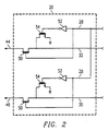
- Figure 2 is a schematic diagram of test isolation circuitry provided on some modules of Figure 1 to selectively isolate some of the testing pads from the remaining functional circuitry during normal operation of the integrated circuit.
- By way of illustration the present invention will be set forth as implemented in a DMD die used in a hard copy device manufactured by Texas Instruments Incorporated of Dallas Texas. This hard copy device implements a DMD type SLM comprising a modular integrated circuit of approximately 5 inches in length. The DMD hard copy product is set forth in Published European Patent document 0,433,981.
- While the present invention is set forth as ideally suited for such a hard copy DMD device, the scope of the present invention is intended to cover all large integrated circuits of modular design, wherein each module can be tested individually with conventional testing equipment, even though the functional testing of some or all modules may depend on the cooperation of other modules.
- Now, with reference to Figure 1, a simplified block diagram of an elongated integrated circuit for use in the hard copy product is shown. The integrated circuit is generally shown at 10 and is seen to comprise a left
control circuit module 12, a rightcontrol circuit module 14, and a plurality of identicalintermediate circuit modules 16. These modules are shown to be interconnected and arranged adjacent to one another and forming a linear array of pixels which may be of the size of 64 by 7,056 pixels. Each ofcircuit modules circuit 10 may be fabricated using the unique process disclosed in Published European Patent document 0,602,634 assigned to the assignee of the present invention. Basically, the elongated 5 inch die is fabricated using a single reticle to step and repeat across a wafer using conventional photolithography techniques. Since each of theintermediate circuit modules 16 forming the mirror array are identical with one another, only three patterns are required of this reticle to expose and fabricate the large elongated integrated circuit as shown in Figure 1. Each ofcircuit modules - According to the present invention, each of
circuit modules testing pads sections 20 of each module are provided in identical locations relative to the module such that standard prober equipment (not shown) can be easily stepped across thecircuit 10 from one module to the next during the testing procedure. The pads for eachsection 20 are identically laid out, and are preferably commonly identified from module to module, as shown. For instance, the left most pad may be identified as the "T" pad of eachtesting pad section 20. The second, third etc. testing pad, as viewed left to right, would also be identically labeled for each testing pad as 20 section as shown. However, each of these testing pads could be used and identified differently from module to module if desired, depending on the circuitry and requirements of the associated module or theoverall circuit 10. - With reference to the left and right
most circuit module logic circuit section 22 and aright logic circuit 24 can be seen to each be electrically coupled to respective testing pads D1 and D2. A gate or switchingcircuit 26 is seen to also be provided on eachcircuit module left gate circuit 26 ofmodule 12 permits pads L1 and L2 of all modules to be selectively electrically connected to leftlogic circuit 22, and theright gate circuit 26 ofmodule 14 permits all pads R1 and R2 to be selectively electrically connected toright logic circuit 24. Each testing pad "T" is seen to be connected to thesegate circuits 26 vialine 28, and are used to selectively enable thesegate sections 26. Whencircuits 26 are enabled, all testing pads L1 and L2 will then become electrically connected tologic circuit 22 vialines logic circuit 24 vialines logic circuitry - Each of
intermediate circuit modules 16 can be seen to have array of pixels represented at 34, such as deflectable micro mirrors which are normally addressed and controlled by thelogic circuitry 22 ofmodule 12, as well as thelogic circuit 24 provided on theright circuit module 14. The control of this array is vialines 36, as shown, which represent row and column address lines, clock lines, read and write lines, etc. - In the foregoing illustration, operation of the
pixel array sections 34 is controlled by bothlogic circuit right circuit modules pixel array section 34 ofcircuit modules 16,circuit conductors appropriate logic circuits respective gating circuitry 26, as shown. A conventional prober (not shown) can access eachtesting pad section 20 in a well known manner, and functionally exerciserespective array 34. Power and ground is provided to integratedcircuit 10 via any of testing pads P and G. - Referring to Figure 2, a schematic representation of the preferred embodiment of each
gate circuitry 26 is shown. although other equivalent circuits are acceptable to achieve the function, whereby thecircuit 26 ofmodule 12 is shown for the purposes of illustration.Gate circuitry 26 comprises a separate MOStransistor switching device 50 in series with each associated signal line, such aslines MOS transistor 50 has its drain terminal connected to the input side, and its source terminal connected to the output side. The gate terminal of eachMOS transistor 50 is connected to the test enableline 28, this test enable line being connected to pad "T" of eachpad section 20 of Figure 1. By enablingtest line 28, each switchingtransistor 50 will be caused to conduct allowing respective signals to pass therethrough from the drain terminal to the source terminal. - When testing of the
integrated circuit 10 is not desired,testing line 28 is grounded on line 42 by a system controller (not shown), thereby causingtransistors 50 to turn off and disconnect the input line from the respective output line.
Therefore, during normal operation ofintegrated circuit 10, thetesting pads 20 can be disconnected from the outside lines connecting the system controller tologic circuits line 28 is inverted by a pair ofinverters 52. The output of eachinverter 52 is connected to the gate terminal of arespective MOS transistor 54.
Grounding pad "T" turnsMOS transistors 54 on. Eachtransistor 54 has its drain terminal grounded, and its source terminal connected to therespective input line
Therefore, when the testing function is disabled by groundingline 28,transistors 54 in turn ground the input lines 30 and 32 to avoid floating. - With the forgoing description of the preferred embodiment of the present invention set forth, a typical testing scenario according to the present invention will now be described.
Afterintegrated circuit 10 has been fabricated, eachintegrated circuit module - The prober equipment is coupled to the appropriate pads of
pad section 20 ofcircuit module 12, and power and ground is applied to the P and G pads ofrespective section 20. Next, an enable signal, such as +5 volts, is applied to test enable pad "T", thereby enabling each ofgate sections 26 oncircuit modules circuitry 22. Aftercircuit module 12 has been tested using a software routine which may be custom designed for this associatedcircuit module 12, the prober equipment is stepped right to thenext circuit module 16 to be tested, and connected to thetesting pad section 20 with associatedmodule circuitry 34. - Again, power and ground is applied to pad P and G to power and enable operation of the entire
integrated circuit 10. Test enable pad T is biased, and appropriate testing signals are provided to thetesting pads 20 to functionally exercise therespective array circuitry 34 of the associatedcircuit module 16. While some testing signals are unswitched and provided directly toarray 34 via respective testing pads D1 and D2 such as clock signals, other testing circuit signals needed to operatearray 34 such as row and column address bits, write and read bits, etc., are provided to the left andright logic circuitry circuit lines respective gating circuitry 26. Of course, thisgating circuitry 26 has first been enabled by applying the appropriate bias to test enable padT. Logic circuits lines 36 toarray 34 which are necessary to exercisearray 34. The testing program implemented emulates the system controller (not shown) normally used to control thecircuit 10 vialines - Thereafter, the prober equipment is stepped right to the
next circuit module 16 to be tested, and the same testing sequence again performed. Finally, the probing equipment will be stepped right to thelast circuit module 14 with the appropriate testing signals being provided to therespective testing pads 20. - Each of the
circuit modules gating circuitry 26 of theleft logic circuit 22 and theright logic circuitry 24, allows complete operation ofintegrated circuit 10 from any of thetesting pads 20 of any ofcircuit modules - While the present invention has been set forth with reference to an elongated DMD integrated circuit such as those implemented in a hard copy device, the scope of the present invention is intended to cover the modular design and method of testing all integrated circuits of non-standard size, and of size greater than that compatible with conventional off-the-shelf prober equipment. Thus, a large integrated circuit having both a large width and length, such as large memory devices, signal processors, microprocessors etc., are also within the scope of the present invention. The integrated circuit is modularized and provided with dedicated testing pads, with each module being individually testable. Some modules are tested with the cooperation of other modules comprising that large integrated circuit. Therefore, the present invention is flexible and can be incorporated into any integrated circuit architecture which can be modularized, such as into arrays or functional subsets.
- While the present invention has been set forth where the testing pads sections are set forth in identical locations from module to module, limitation to identically arranging these testing pad sections is not being inferred. For instance, the testing pads sections can be provided into a lower left corner of one module, a middle location of the next circuit module, and a lower right location of the next circuit module. Testing of each module can still be done individually using conventional prober equipment, whereby these testing pad sections may provide access to control the entire integrated circuit. Some or all of these testing pads can be electrically disconnected from the integrated circuit during normal operation, such as by disabling the gating circuit which connects the testing pads to the circuit module circuit sections. With the present invention, each of the circuit modules can be optically tested as well using conventional technology and equipment.
- While the present invention has been set forth as including only a few testing pads for each pad section, and only a few interconnected and dedicated signal lines, it is to be understood that many testing pads, and many such signal lines are typical in such complex devices, and are suitable with the present invention. In addition, the
gate circuitry 26 can be implemented using other circuit designs to selectively isolate the testing pads from the operational circuit. - Though the invention has been described with respect to a specific preferred embodiment, many variations and modifications will become apparent to those skilled in the art upon reading the present application.
Claims (14)
- A semiconductor integrated circuit comprising; a plurality of interconnected circuit modules, each said module having a circuit section and a dedicated testing pad section coupled to said circuit section.
- The integrated circuit as specified in Claim 1 wherein one said testing pad section is identical to the testing pad section of at least one other module to permit testing of said circuit modules with a single piece of testing equipment.
- The integrated circuit as specified in Claims 1-2, wherein at least two said circuit modules have said testing pad sections commonly located relative to said associated circuit section.
- The integrated circuit as specified in Claims 1-3, further comprising a control circuit connected to one said testing pad section and one said circuit section for selectively electrically isolating said testing pad section from at least one said circuit section.
- The integrated circuit as specified in Claim 4, wherein said control circuit selectively electrically isolates said testing pad section on one said module from said circuit section of other circuit modules.
- The integrated circuit as specified in Claims 1-5, wherein at least one circuit module is not identical to each other circuit module.
- The integrated circuit as specified in Claims 1-6, wherein at least two said circuit modules are identical to one another.
- The integrated circuit as specified in Claim 7, wherein said two identical circuit modules are coupled to a non-identical circuit module.
- The integrated circuit as specified in Claims 1-8, wherein said circuit modules form an elongated integrated circuit having a length greater than 1 inch.
- The integrated circuit as specified in Claims 7-8, wherein said identical circuit modules comprise a spatial light modulator.
- The integrated circuit as specified in Claim 10, wherein said spatial light modulator is comprised of a plurality of micro mirror devices.
- A method of testing an integrated circuit having a plurality of interconnected circuit modules, each module having a circuit section and a dedicated testing pad section coupled to said circuit section, comprising;
connecting test equipment to one said testing pad section;
providing signals to said testing pad section to test said respective circuit section; and
stepping said test equipment to another said circuit module of said integrated circuit and repeating said connecting and providing steps. - The method as specified in Claim 12 further comprising; enabling a control circuit defined on said integrated circuit to electrically connect some portions of said testing pad section to said circuit section.
- The method as specified in Claim 12 further comprising; enabling a control circuit defined on said integrated circuit to electrically connect some portions of said testing pad section to one said circuit section of another said circuit module.
Applications Claiming Priority (2)
| Application Number | Priority Date | Filing Date | Title |
|---|---|---|---|
| US347021 | 1994-11-30 | ||
| US08/347,021 US5648730A (en) | 1994-11-30 | 1994-11-30 | Large integrated circuit with modular probe structures |
Publications (3)
| Publication Number | Publication Date |
|---|---|
| EP0715178A2 true EP0715178A2 (en) | 1996-06-05 |
| EP0715178A3 EP0715178A3 (en) | 1998-01-28 |
| EP0715178B1 EP0715178B1 (en) | 2003-09-03 |
Family
ID=23362000
Family Applications (1)
| Application Number | Title | Priority Date | Filing Date |
|---|---|---|---|
| EP95118691A Expired - Lifetime EP0715178B1 (en) | 1994-11-30 | 1995-11-28 | Integrated circuit comprising a testing pad |
Country Status (6)
| Country | Link |
|---|---|
| US (2) | US5648730A (en) |
| EP (1) | EP0715178B1 (en) |
| JP (1) | JP3883598B2 (en) |
| KR (1) | KR960019643A (en) |
| DE (1) | DE69531657T2 (en) |
| TW (1) | TW320756B (en) |
Cited By (1)
| Publication number | Priority date | Publication date | Assignee | Title |
|---|---|---|---|---|
| US7994806B2 (en) | 2004-12-10 | 2011-08-09 | X-Fab Semiconductor Foundries Ag | System and method for testing embedded circuits with test islands |
Families Citing this family (14)
| Publication number | Priority date | Publication date | Assignee | Title |
|---|---|---|---|---|
| US5619461A (en) | 1995-07-28 | 1997-04-08 | Micron Quantum Devices, Inc. | Memory system having internal state monitoring circuit |
| US5965902A (en) * | 1995-09-19 | 1999-10-12 | Micron Technology | Method and apparatus for testing of dielectric defects in a packaged semiconductor memory device |
| US5657284A (en) | 1995-09-19 | 1997-08-12 | Micron Technology, Inc. | Apparatus and method for testing for defects between memory cells in packaged semiconductor memory devices |
| US5977763A (en) * | 1996-02-27 | 1999-11-02 | Micron Technology, Inc. | Circuit and method for measuring and forcing an internal voltage of an integrated circuit |
| US6229296B1 (en) | 1996-02-27 | 2001-05-08 | Micron Technology, Inc. | Circuit and method for measuring and forcing an internal voltage of an integrated circuit |
| US6946863B1 (en) | 1998-02-27 | 2005-09-20 | Micron Technology, Inc. | Circuit and method for measuring and forcing an internal voltage of an integrated circuit |
| JPH11354594A (en) * | 1998-06-08 | 1999-12-24 | Mitsubishi Electric Corp | Semiconductor device |
| US6163867A (en) * | 1998-08-28 | 2000-12-19 | Hewlett-Packard Company | Input-output pad testing using bi-directional pads |
| EP1227502A1 (en) * | 2001-01-25 | 2002-07-31 | Alcatel | Connection pad arrangements for electronic circuit comprising both functional logic and flash-EEPROM |
| US7026251B2 (en) * | 2001-12-12 | 2006-04-11 | Texas Instruments Incorporated | Method of optimized stitching for digital micro-mirror device |
| US6831772B2 (en) * | 2002-02-01 | 2004-12-14 | Analog Devices, Inc. | Optical mirror module |
| US7026646B2 (en) * | 2002-06-20 | 2006-04-11 | Micron Technology, Inc. | Isolation circuit |
| US6967348B2 (en) * | 2002-06-20 | 2005-11-22 | Micron Technology, Inc. | Signal sharing circuit with microelectric die isolation features |
| DE102004059506B3 (en) | 2004-12-10 | 2006-08-17 | X-Fab Semiconductor Foundries Ag | Arrangement for testing embedded circuits using a separate supply voltage |
Citations (4)
| Publication number | Priority date | Publication date | Assignee | Title |
|---|---|---|---|---|
| EP0332953A2 (en) | 1988-03-16 | 1989-09-20 | Texas Instruments Incorporated | Spatial light modulator and method |
| EP0433981A2 (en) | 1989-12-21 | 1991-06-26 | Texas Instruments Incorporated | Printing system exposure module alignment method and apparatus of manufacture |
| US5079544A (en) | 1989-02-27 | 1992-01-07 | Texas Instruments Incorporated | Standard independent digitized video system |
| EP0602634A1 (en) | 1992-12-16 | 1994-06-22 | Texas Instruments Incorporated | Large die photolithography |
Family Cites Families (17)
| Publication number | Priority date | Publication date | Assignee | Title |
|---|---|---|---|---|
| US4244048A (en) * | 1978-12-29 | 1981-01-06 | International Business Machines Corporation | Chip and wafer configuration and testing method for large-scale-integrated circuits |
| JPS58115372A (en) * | 1981-12-29 | 1983-07-09 | Fujitsu Ltd | Test circuit of semiconductor device |
| JPS60115099A (en) * | 1983-11-25 | 1985-06-21 | Fujitsu Ltd | Semiconductor storage device |
| US5061049A (en) * | 1984-08-31 | 1991-10-29 | Texas Instruments Incorporated | Spatial light modulator and method |
| US4687989A (en) * | 1984-11-01 | 1987-08-18 | Thomson Components-Mostek Corp. | CMOS powerless rom code mask option select |
| DE3526485A1 (en) * | 1985-07-24 | 1987-02-05 | Heinz Krug | CIRCUIT ARRANGEMENT FOR TESTING INTEGRATED CIRCUIT UNITS |
| US4701921A (en) * | 1985-10-23 | 1987-10-20 | Texas Instruments Incorporated | Modularized scan path for serially tested logic circuit |
| US4710931A (en) * | 1985-10-23 | 1987-12-01 | Texas Instruments Incorporated | Partitioned scan-testing system |
| US5214655A (en) * | 1986-09-26 | 1993-05-25 | General Electric Company | Integrated circuit packaging configuration for rapid customized design and unique test capability |
| US4970454A (en) * | 1986-12-09 | 1990-11-13 | Texas Instruments Incorporated | Packaged semiconductor device with test circuits for determining fabrication parameters |
| US5008727A (en) * | 1988-01-22 | 1991-04-16 | Matsushita Electric Industrial Co., Ltd. | Standard cell having test pad for probing and semiconductor integrated circuit device containing the standard cells |
| US4956602A (en) * | 1989-02-14 | 1990-09-11 | Amber Engineering, Inc. | Wafer scale testing of redundant integrated circuit dies |
| US5051996A (en) * | 1989-03-27 | 1991-09-24 | The United States Of America As Represented By The United States Department Of Energy | Built-in-test by signature inspection (bitsi) |
| US5107208A (en) * | 1989-12-19 | 1992-04-21 | North American Philips Corporation | System for partitioning and testing submodule circuits of an integrated circuit |
| US5187712A (en) * | 1990-02-26 | 1993-02-16 | At&T Bell Laboratories | Pseudo-exhaustive self-test technique |
| JP3381929B2 (en) * | 1990-12-27 | 2003-03-04 | 株式会社東芝 | Semiconductor device |
| JP3179595B2 (en) * | 1992-11-12 | 2001-06-25 | 株式会社日立製作所 | Semiconductor integrated circuit device and method of manufacturing the same |
-
1994
- 1994-11-30 US US08/347,021 patent/US5648730A/en not_active Expired - Lifetime
-
1995
- 1995-11-28 DE DE69531657T patent/DE69531657T2/en not_active Expired - Lifetime
- 1995-11-28 EP EP95118691A patent/EP0715178B1/en not_active Expired - Lifetime
- 1995-11-30 JP JP31318295A patent/JP3883598B2/en not_active Expired - Fee Related
- 1995-11-30 KR KR1019950045381A patent/KR960019643A/en not_active Application Discontinuation
-
1996
- 1996-04-12 TW TW085104328A patent/TW320756B/zh not_active IP Right Cessation
- 1996-09-20 US US08/717,035 patent/US5825194A/en not_active Expired - Fee Related
Patent Citations (4)
| Publication number | Priority date | Publication date | Assignee | Title |
|---|---|---|---|---|
| EP0332953A2 (en) | 1988-03-16 | 1989-09-20 | Texas Instruments Incorporated | Spatial light modulator and method |
| US5079544A (en) | 1989-02-27 | 1992-01-07 | Texas Instruments Incorporated | Standard independent digitized video system |
| EP0433981A2 (en) | 1989-12-21 | 1991-06-26 | Texas Instruments Incorporated | Printing system exposure module alignment method and apparatus of manufacture |
| EP0602634A1 (en) | 1992-12-16 | 1994-06-22 | Texas Instruments Incorporated | Large die photolithography |
Cited By (1)
| Publication number | Priority date | Publication date | Assignee | Title |
|---|---|---|---|---|
| US7994806B2 (en) | 2004-12-10 | 2011-08-09 | X-Fab Semiconductor Foundries Ag | System and method for testing embedded circuits with test islands |
Also Published As
| Publication number | Publication date |
|---|---|
| KR960019643A (en) | 1996-06-17 |
| US5825194A (en) | 1998-10-20 |
| TW320756B (en) | 1997-11-21 |
| EP0715178B1 (en) | 2003-09-03 |
| DE69531657D1 (en) | 2003-10-09 |
| JPH08222612A (en) | 1996-08-30 |
| US5648730A (en) | 1997-07-15 |
| DE69531657T2 (en) | 2004-07-29 |
| EP0715178A3 (en) | 1998-01-28 |
| JP3883598B2 (en) | 2007-02-21 |
Similar Documents
| Publication | Publication Date | Title |
|---|---|---|
| EP0715178B1 (en) | Integrated circuit comprising a testing pad | |
| US6847203B1 (en) | Applying parametric test patterns for high pin count ASICs on low pin count testers | |
| US5498978A (en) | Field programmable gate array | |
| US6476628B1 (en) | Semiconductor parallel tester | |
| JP2505049B2 (en) | How to test electronic devices | |
| US5525912A (en) | Probing equipment and a probing method | |
| CN100504974C (en) | Driver circuit for display device | |
| US20030102882A1 (en) | Test apparatuses for semiconductor integrated circuits | |
| US7423443B2 (en) | Method of performing parallel test on semiconductor devices by dividing voltage supply unit | |
| JPH11316264A (en) | Parallel test circuit of semiconductor device | |
| US5892386A (en) | Internal power control circuit for a semiconductor device | |
| JP2010540935A (en) | Method and apparatus for testing a device using a serially controlled intelligent switch | |
| US5796266A (en) | Circuit and a method for configuring pad connections in an integrated device | |
| US5796390A (en) | Redundant shift registers for scanning circuits in liquid crystal display devices | |
| JP3483130B2 (en) | Inspection method for integrated circuits | |
| US20010049805A1 (en) | Circuit, system and method for arranging data output by semicomductor testers to packet-based devices under test | |
| US7010733B2 (en) | Parametric testing for high pin count ASIC | |
| KR100420241B1 (en) | Method and apparatus for testing a semiconductor chip for a image sensor | |
| US6363508B1 (en) | Method for testing reflection LCD projector and display panel pixel area thereof | |
| JP3853448B2 (en) | Semiconductor memory device | |
| JP2818546B2 (en) | Semiconductor integrated circuit | |
| JP2633692B2 (en) | Semiconductor test method | |
| KR100455731B1 (en) | Wafer burn-in test apparatus to simultaneously burn-in every die in one wafer by one probing process | |
| KR100505613B1 (en) | Printed circuit board for performing burn-in test of semiconductor memory device | |
| JPS6158254A (en) | Semiconductor integrated circuit device |
Legal Events
| Date | Code | Title | Description |
|---|---|---|---|
| PUAI | Public reference made under article 153(3) epc to a published international application that has entered the european phase |
Free format text: ORIGINAL CODE: 0009012 |
|
| AK | Designated contracting states |
Kind code of ref document: A2 Designated state(s): DE FR GB IT NL |
|
| PUAL | Search report despatched |
Free format text: ORIGINAL CODE: 0009013 |
|
| AK | Designated contracting states |
Kind code of ref document: A3 Designated state(s): DE FR GB IT NL |
|
| RHK1 | Main classification (correction) |
Ipc: G06F 11/267 |
|
| 17P | Request for examination filed |
Effective date: 19980514 |
|
| 17Q | First examination report despatched |
Effective date: 20020412 |
|
| GRAH | Despatch of communication of intention to grant a patent |
Free format text: ORIGINAL CODE: EPIDOS IGRA |
|
| GRAS | Grant fee paid |
Free format text: ORIGINAL CODE: EPIDOSNIGR3 |
|
| GRAA | (expected) grant |
Free format text: ORIGINAL CODE: 0009210 |
|
| AK | Designated contracting states |
Kind code of ref document: B1 Designated state(s): DE FR GB IT NL |
|
| PG25 | Lapsed in a contracting state [announced via postgrant information from national office to epo] |
Ref country code: NL Free format text: LAPSE BECAUSE OF FAILURE TO SUBMIT A TRANSLATION OF THE DESCRIPTION OR TO PAY THE FEE WITHIN THE PRESCRIBED TIME-LIMIT Effective date: 20030903 Ref country code: IT Free format text: LAPSE BECAUSE OF FAILURE TO SUBMIT A TRANSLATION OF THE DESCRIPTION OR TO PAY THE FEE WITHIN THE PRESCRIBED TIME-LIMIT;WARNING: LAPSES OF ITALIAN PATENTS WITH EFFECTIVE DATE BEFORE 2007 MAY HAVE OCCURRED AT ANY TIME BEFORE 2007. THE CORRECT EFFECTIVE DATE MAY BE DIFFERENT FROM THE ONE RECORDED. Effective date: 20030903 Ref country code: FR Free format text: LAPSE BECAUSE OF FAILURE TO SUBMIT A TRANSLATION OF THE DESCRIPTION OR TO PAY THE FEE WITHIN THE PRESCRIBED TIME-LIMIT Effective date: 20030903 |
|
| REG | Reference to a national code |
Ref country code: GB Ref legal event code: FG4D |
|
| REF | Corresponds to: |
Ref document number: 69531657 Country of ref document: DE Date of ref document: 20031009 Kind code of ref document: P |
|
| NLV1 | Nl: lapsed or annulled due to failure to fulfill the requirements of art. 29p and 29m of the patents act | ||
| PLBE | No opposition filed within time limit |
Free format text: ORIGINAL CODE: 0009261 |
|
| STAA | Information on the status of an ep patent application or granted ep patent |
Free format text: STATUS: NO OPPOSITION FILED WITHIN TIME LIMIT |
|
| 26N | No opposition filed |
Effective date: 20040604 |
|
| EN | Fr: translation not filed | ||
| PGFP | Annual fee paid to national office [announced via postgrant information from national office to epo] |
Ref country code: DE Payment date: 20101130 Year of fee payment: 16 |
|
| PGFP | Annual fee paid to national office [announced via postgrant information from national office to epo] |
Ref country code: GB Payment date: 20101022 Year of fee payment: 16 |
|
| GBPC | Gb: european patent ceased through non-payment of renewal fee |
Effective date: 20111128 |
|
| REG | Reference to a national code |
Ref country code: DE Ref legal event code: R119 Ref document number: 69531657 Country of ref document: DE Effective date: 20120601 |
|
| PG25 | Lapsed in a contracting state [announced via postgrant information from national office to epo] |
Ref country code: GB Free format text: LAPSE BECAUSE OF NON-PAYMENT OF DUE FEES Effective date: 20111128 |
|
| PG25 | Lapsed in a contracting state [announced via postgrant information from national office to epo] |
Ref country code: DE Free format text: LAPSE BECAUSE OF NON-PAYMENT OF DUE FEES Effective date: 20120601 |