EP0703079A2 - Reducing energy variations in thermal ink jet printheads - Google Patents
Reducing energy variations in thermal ink jet printheads Download PDFInfo
- Publication number
- EP0703079A2 EP0703079A2 EP95305701A EP95305701A EP0703079A2 EP 0703079 A2 EP0703079 A2 EP 0703079A2 EP 95305701 A EP95305701 A EP 95305701A EP 95305701 A EP95305701 A EP 95305701A EP 0703079 A2 EP0703079 A2 EP 0703079A2
- Authority
- EP
- European Patent Office
- Prior art keywords
- resistors
- printhead
- output
- pulse
- energy
- Prior art date
- Legal status (The legal status is an assumption and is not a legal conclusion. Google has not performed a legal analysis and makes no representation as to the accuracy of the status listed.)
- Granted
Links
Images

Classifications
-
- B—PERFORMING OPERATIONS; TRANSPORTING
- B41—PRINTING; LINING MACHINES; TYPEWRITERS; STAMPS
- B41J—TYPEWRITERS; SELECTIVE PRINTING MECHANISMS, i.e. MECHANISMS PRINTING OTHERWISE THAN FROM A FORME; CORRECTION OF TYPOGRAPHICAL ERRORS
- B41J2/00—Typewriters or selective printing mechanisms characterised by the printing or marking process for which they are designed
- B41J2/005—Typewriters or selective printing mechanisms characterised by the printing or marking process for which they are designed characterised by bringing liquid or particles selectively into contact with a printing material
- B41J2/01—Ink jet
- B41J2/015—Ink jet characterised by the jet generation process
- B41J2/04—Ink jet characterised by the jet generation process generating single droplets or particles on demand
- B41J2/045—Ink jet characterised by the jet generation process generating single droplets or particles on demand by pressure, e.g. electromechanical transducers
- B41J2/04501—Control methods or devices therefor, e.g. driver circuits, control circuits
- B41J2/04541—Specific driving circuit
-
- B—PERFORMING OPERATIONS; TRANSPORTING
- B41—PRINTING; LINING MACHINES; TYPEWRITERS; STAMPS
- B41J—TYPEWRITERS; SELECTIVE PRINTING MECHANISMS, i.e. MECHANISMS PRINTING OTHERWISE THAN FROM A FORME; CORRECTION OF TYPOGRAPHICAL ERRORS
- B41J2/00—Typewriters or selective printing mechanisms characterised by the printing or marking process for which they are designed
- B41J2/005—Typewriters or selective printing mechanisms characterised by the printing or marking process for which they are designed characterised by bringing liquid or particles selectively into contact with a printing material
- B41J2/01—Ink jet
- B41J2/015—Ink jet characterised by the jet generation process
- B41J2/04—Ink jet characterised by the jet generation process generating single droplets or particles on demand
- B41J2/045—Ink jet characterised by the jet generation process generating single droplets or particles on demand by pressure, e.g. electromechanical transducers
- B41J2/04501—Control methods or devices therefor, e.g. driver circuits, control circuits
- B41J2/04543—Block driving
-
- B—PERFORMING OPERATIONS; TRANSPORTING
- B41—PRINTING; LINING MACHINES; TYPEWRITERS; STAMPS
- B41J—TYPEWRITERS; SELECTIVE PRINTING MECHANISMS, i.e. MECHANISMS PRINTING OTHERWISE THAN FROM A FORME; CORRECTION OF TYPOGRAPHICAL ERRORS
- B41J2/00—Typewriters or selective printing mechanisms characterised by the printing or marking process for which they are designed
- B41J2/005—Typewriters or selective printing mechanisms characterised by the printing or marking process for which they are designed characterised by bringing liquid or particles selectively into contact with a printing material
- B41J2/01—Ink jet
- B41J2/015—Ink jet characterised by the jet generation process
- B41J2/04—Ink jet characterised by the jet generation process generating single droplets or particles on demand
- B41J2/045—Ink jet characterised by the jet generation process generating single droplets or particles on demand by pressure, e.g. electromechanical transducers
- B41J2/04501—Control methods or devices therefor, e.g. driver circuits, control circuits
- B41J2/04568—Control according to number of actuators used simultaneously
-
- B—PERFORMING OPERATIONS; TRANSPORTING
- B41—PRINTING; LINING MACHINES; TYPEWRITERS; STAMPS
- B41J—TYPEWRITERS; SELECTIVE PRINTING MECHANISMS, i.e. MECHANISMS PRINTING OTHERWISE THAN FROM A FORME; CORRECTION OF TYPOGRAPHICAL ERRORS
- B41J2/00—Typewriters or selective printing mechanisms characterised by the printing or marking process for which they are designed
- B41J2/005—Typewriters or selective printing mechanisms characterised by the printing or marking process for which they are designed characterised by bringing liquid or particles selectively into contact with a printing material
- B41J2/01—Ink jet
- B41J2/015—Ink jet characterised by the jet generation process
- B41J2/04—Ink jet characterised by the jet generation process generating single droplets or particles on demand
- B41J2/045—Ink jet characterised by the jet generation process generating single droplets or particles on demand by pressure, e.g. electromechanical transducers
- B41J2/04501—Control methods or devices therefor, e.g. driver circuits, control circuits
- B41J2/0458—Control methods or devices therefor, e.g. driver circuits, control circuits controlling heads based on heating elements forming bubbles
-
- B—PERFORMING OPERATIONS; TRANSPORTING
- B41—PRINTING; LINING MACHINES; TYPEWRITERS; STAMPS
- B41J—TYPEWRITERS; SELECTIVE PRINTING MECHANISMS, i.e. MECHANISMS PRINTING OTHERWISE THAN FROM A FORME; CORRECTION OF TYPOGRAPHICAL ERRORS
- B41J2/00—Typewriters or selective printing mechanisms characterised by the printing or marking process for which they are designed
- B41J2/005—Typewriters or selective printing mechanisms characterised by the printing or marking process for which they are designed characterised by bringing liquid or particles selectively into contact with a printing material
- B41J2/01—Ink jet
- B41J2/015—Ink jet characterised by the jet generation process
- B41J2/04—Ink jet characterised by the jet generation process generating single droplets or particles on demand
- B41J2/045—Ink jet characterised by the jet generation process generating single droplets or particles on demand by pressure, e.g. electromechanical transducers
- B41J2/04501—Control methods or devices therefor, e.g. driver circuits, control circuits
- B41J2/04591—Width of the driving signal being adjusted
Definitions
- This invention relates to thermal inkjet printing, and, in particular, to minimizing variations of the energy delivered to printhead resistive heaters.
- Thermal inkjet (TIJ) printing involves propelling minute, closely spaced jets of ink onto a printing surface, which is usually paper.
- a TIJ printhead contains a reservoir of ink connected with a series of nozzles which are used to form the jets. By controlling both the movement of the printhead across the paper and also which jets are activated at any given time, a printer can form alphabetic characters and graphic images.
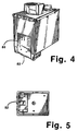
- a typical TIJ printhead is shown in Fig. 4. This is a disposable unit with its ink supply contained within its plastic housing. To form each jet, a tubular nozzle is mounted with its internal end communicating with the ink reservoir and its external end close to the paper. These nozzles are organized into banks or rows 82, two of which may be seen in the end view of the printhead in Fig. 5.
- a small resistor of a size comparable to the diameter of the nozzle, is mounted in the ink reservoir close to the internal end of each nozzle. When a pulse of electrical energy is sent to the resistor, its rapid heating boils the adjacent ink, forming a minute bubble. The growth of this bubble forces a small quantity of ink through the nozzle and onto the paper. Electrical pulses are supplied to the printhead via a collection of small conductive areas 80 which mate with corresponding contacts in the printer. The resistors in the printhead may thus be activated in any desired combination.
- a factor affecting the operation of a TIJ printhead is that not all available resistors in a resistor bank in the printhead are simultaneously energized. Only a subset - its composition dependent on the printable data - from the total set of resistors in the bank is "fired" during a particular pulse.
- the energy source supplying the printhead is modeled as a voltage source Vs (12) with a series impedance Zs (14), then the amount of energy supplied to any given resistor 10 will vary with the number of its neighbors which are also energized during that pulse.
- a typical bank might contain 20 resistors. Thus, from 1 to 20 of these may be pulsed by closing the respective switch(es) 16. This load variation puts stringent demands on the regulation of the energy source.
- an output capacitor provides low impedance at high frequencies. But the series resistance of this capacitor is not negligible; neither is that of the connecting cabling linking the printhead with its driver. These resistances, together with other parasitic resistances, limit the achievable reduction in output impedance.
- One embodiment of the present invention addresses the problem of delivering, from a common power supply, pulses of constant energy to a set of resistors which can be individually switched across the supply, as shown in Fig. 1. If subsets of resistors are switched on in a sequence according to some known schedule, such as occurs in TIJ printing, it is not necessary to use a feedback loop, with its attendant speed limitations, to compensate for load variations. The effect of load variations can be compensated instantaneously.
- the invention uses a practical and inexpensive method for doing this: adjusting the pulse width.
- all the resistors are nominally equal in value.
- the total conductance of the switched-on subset is determined by multiplying the number of resistors in the subset by the conductance of an individual resistor. The total conductance determines the pulse width through use of a compensation relation formula or lookup table.
- Different compensation relations may be used to determine the pulse width variation.
- the simplest is to vary the pulse width linearly with the load conductance.
- the energy absorbed by a pulsed resistor varies (a) as the square of the voltage across it, and (b) linearly with the pulse width.
- the load voltage varies approximately inversely with the load conductance.
- precise compensation can be obtained by determining exactly how the load voltage varies with load conductance and varying the pulse width inversely with the square of the load voltage.
- the set of resistors contains resistors of different values.
- the conductances of all the resistors in the set are stored in a lookup table. When a particular subset is chosen to be the load, the conductance values of all the subset members are retrieved from the table and added.
- the pulse width is then determined from the sum value by a compensation relation.
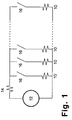
- Fig. 1 is a simplified TIJ printing arrangement, showing an energy source supplying individually switched printhead resistors.
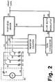
- Fig. 2 is a diagram of an apparatus according to a preferred embodiment of the invention.
- Fig. 3 is a diagram of an apparatus according to another embodiment of the invention having resistors of differing values.
- Fig. 4 is an isometric view of a replaceable TIJ printhead.
- Fig. 5 is an end view of the printhead of Fig. 4.
- An energy source 20 is modelled as a voltage source Vs (12) with a known series impedance Zs (14).
- the source is a regulated DC power supply of about 12 volts output, whose output impedance (at high frequencies; see previous discussion) is determined by the series resistance of a filter capacitor, about half an ohm. To this resistance is added that of a flexible cable used to connect to the moving printhead, plus other connectors.
- a set of nominally equal-valued printhead resistors 40 Connected to the source 20 is a set of nominally equal-valued printhead resistors 40, each having a switch 42 by which it can be connected across the source 20. These resistors share a common return path 48, so that those which are switched across the source are in parallel.
- the nominal value of the resistors is thirty ohms.
- the distribution of production values is Gaussian, but the distribution tails are truncated, as printheads with resistor values beyond about ⁇ 10% of the nominal are rejected.
- each resistor is submerged in an ink reservoir.
- a resistor When a resistor is energized by pulsing its switch, it boils the ink in contact with it, forming a minute bubble whose expansion forces liquid ink through an adjacent nozzle and onto a print medium such as paper.
- the resistors and nozzles are arranged in sets of columns called "primitives". Although 10 to 25 resistors would commonly comprise one primitive, only four resistors are shown in Fig. 2 for drawing simplicity. The principles of the invention remain the same for any number of resistors.
- Switches 42 are activated by control signals connected via lines 44.
- Control output lines 44 are energized by printhead driver circuit 21, whose input 22 is the data to be printed.
- Printhead driver circuit 21 determines, from the print data, just which subset of resistors is to be energized during a pulse. Depending on this print data, from 0 to 4 resistors may be chosen, in various combinations.
- Driver 21 also has an enable input 46 to govern when lines 44 may be activated.
- resistor counter 23 Also connected to control lines 40 is the resistor counter 23. Its circuitry determines the number of resistors being energized during a pulse. This number is supplied as an input to data converter 25, which uses a compensation relation formula to determine a corresponding pulse width. Data converter can compute the pulse width, or the proper pulse width for each possible number of energized resistors can be pre-computed, stored in a lookup table, and retrieved as needed. The latter method is often faster when the compensation relation is complex.
- Pulse width modulator (PWM) 26 generates a timing signal on its output 27. This timing signal is initiated by the print data on start input 28, and its width corresponds to the information supplied by data converter 25 to width control input 24. The timing signal is supplied as the enable signal to printhead driver circuit 21 to regulate the width that the selected switches are closed.
- a typical print cycle begins with the arrival of print data to input 22 of printhead driver 21 and to width control input 28 of PWM 26. This event initiates a timing signal on output 27 of PWM 26.
- printhead driver 21 chooses the proper subset of resistors, and the timing signal enables the corresponding control lines 44 to close their switches, thus supplying energy to the subset.
- Resistor counter 23 by monitoring the control lines 44, determines the number of activated resistors, and supplies this number to data converter 25.
- Data converter 25 according to its internal rule or algorithm (explained below) determines an appropriate timing signal duration and supplies this information to PWM 26 at its width control input 24.
- Data converter 25 can use table lookup means or computation to implement its internal algorithm.
- the function of data converter 25 is cooperating to counteract the variation in the pulsed energy supplied to a resistor, depending on whether it is selected alone, or has 1, 2, or 3 other resistors selected with it. As more resistors are switched on, the voltage across each one is reduced because of the increased voltage drop across Zs (14), which subtracts from the available voltage Vs (12). This reduces the power supplied to a resistor; the energy supplied is also reduced, since this is simply power times the pulse width.
- Data converter 25 operates to extend the pulse width as more resistors are selected. There are various choices of how to vary the pulse width as a function of the number of resistors selected. To make this choice, it is helpful to understand the energy variation in more detail.
- Equation (2) is exact.
- Equation (3) just as the exact Equation (2), describes the reduction of energy in a resistor as more resistors are added. However, it also suggests that there is a choice of algorithms that can be installed in data converter 25 for increasing pulse width T to compensate for this reduction.
- a linear compensation rule proves to be adequate for the desired print quality
- data converter 25 is a lookup table with pre-computed output values corresponding to all possible subset sizes.
- PWM 26 adjusts the pulse width in discrete steps.
- data converter 25 presets a counter. This counter, advanced by the system clock, terminates the pulse when it reaches its end count. The accuracy of this approach is quite adequate, with the clock allowing a time resolution of about 50 nanoseconds out of a pulse width of several microseconds.
- the load resistors have different values. Referring to Fig. 3, load resistors 50-53 are now presumed to differ in value. Although the problem is similiar to that already discussed for the case of nominally equal values of resistance, what is required here is more than knowing the number of resistors selected during a pulse cycle. Their individual values must also be known in order to compute the total load on the source, and, therefore, the voltage drop in Zs.
- a conductance table 30 stores the values of conductance for each resistor in the set.
- load driver 35 chooses a subset based on data at its input 22, control lines 70-73 inform table 30 which resistors comprise the subset.
- the conductance value of each member of the subset is looked up in table 30 and this data is passed to a data combiner (here called a conductance sum block 31), which adds the values to determine the total load (as a conductance) on the source.
- Values of conductance, rather than resistance, are stored because of the ease of calculating the total load by a simple summing operation. Alternatively, values of resistance can be stored, but calculating the total load resistance is more complicated.
- data combiner refers to the operation of summing conductances, or the invert-sum-invert operation needed if values of resistance are stored.
- the sum value is passed to data converter 36, which, in the same manner as in the previous embodiment, determines the increase in pulse width needed to maintain the pulsed energy constant, or nearly so.
- data converter 36 determines the increase in pulse width needed to maintain the pulsed energy constant, or nearly so.
- PWM 26 furnishes, via output 27, a variable-duration timing signal to enable input 37 of the load driver.
- PWM 26 receives start and pulse width information through its inputs 28 and 24, respectively.
Abstract
Description
- This invention relates to thermal inkjet printing, and, in particular, to minimizing variations of the energy delivered to printhead resistive heaters.
- Thermal inkjet (TIJ) printing involves propelling minute, closely spaced jets of ink onto a printing surface, which is usually paper. A TIJ printhead contains a reservoir of ink connected with a series of nozzles which are used to form the jets. By controlling both the movement of the printhead across the paper and also which jets are activated at any given time, a printer can form alphabetic characters and graphic images.
- A typical TIJ printhead is shown in Fig. 4. This is a disposable unit with its ink supply contained within its plastic housing. To form each jet, a tubular nozzle is mounted with its internal end communicating with the ink reservoir and its external end close to the paper. These nozzles are organized into banks or
rows 82, two of which may be seen in the end view of the printhead in Fig. 5. A small resistor, of a size comparable to the diameter of the nozzle, is mounted in the ink reservoir close to the internal end of each nozzle. When a pulse of electrical energy is sent to the resistor, its rapid heating boils the adjacent ink, forming a minute bubble. The growth of this bubble forces a small quantity of ink through the nozzle and onto the paper. Electrical pulses are supplied to the printhead via a collection of smallconductive areas 80 which mate with corresponding contacts in the printer. The resistors in the printhead may thus be activated in any desired combination. - To maintain good print quality, it is essential that the bubble formation and subsequent ink ejection remain very consistent over a large number of operations. Although there are many variables which affect this process, one of the most important is the amount of energy supplied to the resistor each time it is pulsed; this energy must be constant, or nearly so. Below a certain energy limit, the bubble does not form properly, and above another limit, there is thermal damage to the resistor.
- A factor affecting the operation of a TIJ printhead is that not all available resistors in a resistor bank in the printhead are simultaneously energized. Only a subset - its composition dependent on the printable data - from the total set of resistors in the bank is "fired" during a particular pulse. Referring now to Fig. 1, if the energy source supplying the printhead is modeled as a voltage source Vs (12) with a series impedance Zs (14), then the amount of energy supplied to any given
resistor 10 will vary with the number of its neighbors which are also energized during that pulse. A typical bank might contain 20 resistors. Thus, from 1 to 20 of these may be pulsed by closing the respective switch(es) 16. This load variation puts stringent demands on the regulation of the energy source. - An excellent reference for information on TIJ printing is the October, 1988 issue of the Hewlett-Packard Journal. This includes additional pictures of printheads and other elements of a TIJ printer, as well as diagrams and technical discussions of numerous design concerns. In particular, the article Integrating the Printhead into the HP DeskJet Printer, page 62ff, discusses prior-art attempts to deal with the variable-energy problem solved by this invention. According to the article, the solution chosen was to limit the maximum size of a resistor bank to four. As will be seen by a study of the present disclosure, such a limitation is overcome by the principles of the invention.
- To keep the energy constant in a
printhead resistor 16 each time it is pulsed, regardless of how many other resistors are also pulsed at the same time, is a problem that calls for an inexpensive and readily implemented solution. - One conventional response to this problem is to provide a regulated power supply with load voltage sensing. But, since pulse width (pulse time duration) in TIJ printing is typically just a few microseconds, this requires an expensive regulator with wide loop bandwidth to track the rapid load variations.
- In a less expensive regulated supply, an output capacitor provides low impedance at high frequencies. But the series resistance of this capacitor is not negligible; neither is that of the connecting cabling linking the printhead with its driver. These resistances, together with other parasitic resistances, limit the achievable reduction in output impedance.
- One embodiment of the present invention addresses the problem of delivering, from a common power supply, pulses of constant energy to a set of resistors which can be individually switched across the supply, as shown in Fig. 1. If subsets of resistors are switched on in a sequence according to some known schedule, such as occurs in TIJ printing, it is not necessary to use a feedback loop, with its attendant speed limitations, to compensate for load variations. The effect of load variations can be compensated instantaneously. The invention uses a practical and inexpensive method for doing this: adjusting the pulse width.
- In an embodiment of the invention, all the resistors are nominally equal in value. The total conductance of the switched-on subset is determined by multiplying the number of resistors in the subset by the conductance of an individual resistor. The total conductance determines the pulse width through use of a compensation relation formula or lookup table.
- Different compensation relations may be used to determine the pulse width variation. The simplest is to vary the pulse width linearly with the load conductance. However, the energy absorbed by a pulsed resistor varies (a) as the square of the voltage across it, and (b) linearly with the pulse width. But, because of the source impedance, the load voltage varies approximately inversely with the load conductance. Hence, more accurate energy compensation can be obtained by varying the pulse width in square-law relation to the conductance. Furthermore, precise compensation can be obtained by determining exactly how the load voltage varies with load conductance and varying the pulse width inversely with the square of the load voltage. These or other relations may be employed in the invention.
- When a microprocessor or other digital hardware is used to implement the principles of the invention, it is convenient to use a compensation relation that varies the pulse width in discrete steps. The resolution of the pulse width adjustment, and hence the accuracy of the compensation, is improved for high controller clock rates and correspondingly smaller clock periods.
- In another embodiment of the invention, the set of resistors contains resistors of different values. The conductances of all the resistors in the set are stored in a lookup table. When a particular subset is chosen to be the load, the conductance values of all the subset members are retrieved from the table and added.
- The pulse width is then determined from the sum value by a compensation relation.
- Fig. 1 is a simplified TIJ printing arrangement, showing an energy source supplying individually switched printhead resistors.
- Fig. 2 is a diagram of an apparatus according to a preferred embodiment of the invention.
- Fig. 3 is a diagram of an apparatus according to another embodiment of the invention having resistors of differing values.
- Fig. 4 is an isometric view of a replaceable TIJ printhead.
- Fig. 5 is an end view of the printhead of Fig. 4.
- Refer now to Fig. 2, which shows a preferred embodiment of the invention. An
energy source 20 is modelled as a voltage source Vs (12) with a known series impedance Zs (14). In this embodiment, the source is a regulated DC power supply of about 12 volts output, whose output impedance (at high frequencies; see previous discussion) is determined by the series resistance of a filter capacitor, about half an ohm. To this resistance is added that of a flexible cable used to connect to the moving printhead, plus other connectors. - Connected to the
source 20 is a set of nominally equal-valuedprinthead resistors 40, each having aswitch 42 by which it can be connected across thesource 20. These resistors share acommon return path 48, so that those which are switched across the source are in parallel. The nominal value of the resistors is thirty ohms. The distribution of production values is Gaussian, but the distribution tails are truncated, as printheads with resistor values beyond about ±10% of the nominal are rejected. - In TIJ printing, each resistor is submerged in an ink reservoir. When a resistor is energized by pulsing its switch, it boils the ink in contact with it, forming a minute bubble whose expansion forces liquid ink through an adjacent nozzle and onto a print medium such as paper. In the printhead, the resistors and nozzles are arranged in sets of columns called "primitives". Although 10 to 25 resistors would commonly comprise one primitive, only four resistors are shown in Fig. 2 for drawing simplicity. The principles of the invention remain the same for any number of resistors.
-
Switches 42 are activated by control signals connected vialines 44.Control output lines 44 are energized byprinthead driver circuit 21, whoseinput 22 is the data to be printed.Printhead driver circuit 21 determines, from the print data, just which subset of resistors is to be energized during a pulse. Depending on this print data, from 0 to 4 resistors may be chosen, in various combinations.Driver 21 also has an enableinput 46 to govern whenlines 44 may be activated. - Also connected to control
lines 40 is theresistor counter 23. Its circuitry determines the number of resistors being energized during a pulse. This number is supplied as an input todata converter 25, which uses a compensation relation formula to determine a corresponding pulse width. Data converter can compute the pulse width, or the proper pulse width for each possible number of energized resistors can be pre-computed, stored in a lookup table, and retrieved as needed. The latter method is often faster when the compensation relation is complex. - Pulse width modulator (PWM) 26 generates a timing signal on its
output 27. This timing signal is initiated by the print data onstart input 28, and its width corresponds to the information supplied bydata converter 25 towidth control input 24. The timing signal is supplied as the enable signal toprinthead driver circuit 21 to regulate the width that the selected switches are closed. - A typical print cycle begins with the arrival of print data to input 22 of
printhead driver 21 and towidth control input 28 ofPWM 26. This event initiates a timing signal onoutput 27 ofPWM 26. At the same time,printhead driver 21 chooses the proper subset of resistors, and the timing signal enables thecorresponding control lines 44 to close their switches, thus supplying energy to the subset.Resistor counter 23, by monitoring thecontrol lines 44, determines the number of activated resistors, and supplies this number todata converter 25.Data converter 25, according to its internal rule or algorithm (explained below) determines an appropriate timing signal duration and supplies this information toPWM 26 at itswidth control input 24.Data converter 25 can use table lookup means or computation to implement its internal algorithm. When the determined time duration is reached,PWM 26 terminates the timing signal, causing the switches to open. - The function of
data converter 25 is cooperating to counteract the variation in the pulsed energy supplied to a resistor, depending on whether it is selected alone, or has 1, 2, or 3 other resistors selected with it. As more resistors are switched on, the voltage across each one is reduced because of the increased voltage drop across Zs (14), which subtracts from the available voltage Vs (12). This reduces the power supplied to a resistor; the energy supplied is also reduced, since this is simply power times the pulse width.Data converter 25 operates to extend the pulse width as more resistors are selected. There are various choices of how to vary the pulse width as a function of the number of resistors selected. To make this choice, it is helpful to understand the energy variation in more detail. - If a single resistor is selected, the energy it dissipates during the pulse (assuming that impedance Zs is resistive) is

where
R is the common resistor value
T is the pulse width. - In general, for M resistors connected across the source, the energy dissipated in each resistor is

- Equation (2) is exact. By re-arranging and expanding this expression, another form is obtained which shows clearly the dependency of the energy on the number M of load resistors; the energy dissipated in each resistor is

where
M = 1, 2, 3, ····
a = Zs/R - Expression (3), just as the exact Equation (2), describes the reduction of energy in a resistor as more resistors are added. However, it also suggests that there is a choice of algorithms that can be installed in
data converter 25 for increasing pulse width T to compensate for this reduction. - By increasing T inversely as the first 2 terms in the parentheses, a linear correction of the energy reduction may be obtained. This is the simplest algorithm to implement and may be adequate in many applications, especially if a = Zs/R is much less than unity. By adding the third term, a square-law correction is obtained, which is probably satisfactory for most applications. But, if exact correction is needed, it can be obtained by embodying Equation (2) in
data converter 25. - In the described preferred embodiment, a linear compensation rule proves to be adequate for the desired print quality, and
data converter 25 is a lookup table with pre-computed output values corresponding to all possible subset sizes. - In TIJ printer applications, it is common to implement all or most control functions with digital hardware and/or a microprocessor. Such is the case in this embodiment . In this case,
PWM 26 adjusts the pulse width in discrete steps. In the implementation of the PWM,data converter 25 presets a counter. This counter, advanced by the system clock, terminates the pulse when it reaches its end count. The accuracy of this approach is quite adequate, with the clock allowing a time resolution of about 50 nanoseconds out of a pulse width of several microseconds. - In another embodiment of the invention, the load resistors have different values. Referring to Fig. 3, load resistors 50-53 are now presumed to differ in value. Although the problem is similiar to that already discussed for the case of nominally equal values of resistance, what is required here is more than knowing the number of resistors selected during a pulse cycle. Their individual values must also be known in order to compute the total load on the source, and, therefore, the voltage drop in Zs.
- In this embodiment, a conductance table 30 stores the values of conductance for each resistor in the set. When
load driver 35 chooses a subset based on data at itsinput 22, control lines 70-73 inform table 30 which resistors comprise the subset. The conductance value of each member of the subset is looked up in table 30 and this data is passed to a data combiner (here called a conductance sum block 31), which adds the values to determine the total load (as a conductance) on the source. - Values of conductance, rather than resistance, are stored because of the ease of calculating the total load by a simple summing operation. Alternatively, values of resistance can be stored, but calculating the total load resistance is more complicated. The term "data combiner" refers to the operation of summing conductances, or the invert-sum-invert operation needed if values of resistance are stored.
- The sum value is passed to
data converter 36, which, in the same manner as in the previous embodiment, determines the increase in pulse width needed to maintain the pulsed energy constant, or nearly so. When there are many load resistors (more than the four used here for illustrative simplicity), it is likely thatdata converter 36 will compute the required pulse width, rather than rely on a precomputed lookup table. This is because the number of possible values of total load conductance (or resistance) grows rapidly with the size of the resistor set. - In similiar fashion to the preferred embodiment already described,
PWM 26 furnishes, viaoutput 27, a variable-duration timing signal to enableinput 37 of the load driver.PWM 26 receives start and pulse width information through itsinputs - We have described and illustrated the principles of our invention with reference to a preferred embodiment and an additional embodiment; however, it will be apparent that the invention can be modified in arrangement and detail without departing from such principles. For instance, the energy source can be modelled as a current source with a parallel impedance. It will be recognized that the detailed embodiment is illustrative only, and should not be taken as limiting the scope of my invention. Rather, we claim as our invention all such variations as may fall within the scope and spirit of the following claims and equivalents thereto.
Claims (10)
- Apparatus for driving a printhead in a thermal inkjet (TIJ) printer wherein an energy source (20) of known impedance (14) supplies a pulse of energy to the printhead, comprising:
a set of nominally equal-valued resistors (40) in the printhead, each resistor having an associated switch (42) for connecting the resistor (40) to the energy source (20), and the set sharing a common return path (48), wherein a subset of resistors receives a pulse of energy by simultaneous action of the corresponding switches (42);
a printhead driver (21) having an input (22) coupled to a source of print data, control outputs (44) coupled to the set of resistor switches (42), and an enable input (46);
a counter (23) coupled to the printhead driver (21) and responsive to the number of resistors comprising the subset to be connected to the energy source, having an output;
a data converter (25) having an input coupled to the counter output and an output representing a value of pulse width, the value being responsive to the counter output; and
a pulse width modulator (26) having a start input (28) coupled to the source of print data, a width control input (24) coupled to the data converter (25) output, and an output (27) coupled to the enable input (46) of the printhead driver (21). - Apparatus for driving a TIJ printhead, as recited in claim 1, wherein the value of pulse width responds linearly to the counter (23) output.
- Apparatus for driving a TIJ printhead, as recited in claim 1, wherein the value of pulse width responds in square-law relation to the counter (23) output.
- A method for driving a printhead in a thermal inkjet (TIJ) printing apparatus wherein an energy source (20) of known impedance (14) supplies a pulse of energy to a selected subset of a set of resistors (40) of nominally equal value in the printhead, comprising the steps of:
determining the number of resistors in the subset;
selecting a pulse width in response to the determined number of resistors; and
driving the subset of resistors with an energy pulse having the selected width. - A method for driving a TIJ printhead, as recited in claim 4, wherein the pulse width is selected as a linear response to the number of resistors in the subset.
- A method for driving a TIJ printhead, as recited in claim 5, wherein the pulse width is selected in discrete steps.
- A method for driving a TIJ printhead, as recited in claim 4, wherein the pulse width is selected as a square-law response to the number of resistors in the subset.
- A method for driving a TIJ printhead, as recited in claim 7, wherein the pulse width is selected in discrete steps.
- A method for driving a subset of resistors in apparatus comprising an energy source (20) of known impedance (14) and a set of resistors (50-53) sharing a common return path (48), each resistor having a switch (60-63) for connecting to the energy source (20), wherein the subset of resistors receives an energy pulse by simultaneous action of the corresponding switches (60-63), the method comprising the steps of:
storing, in a lookup table (30), the value of conductance of each resistor in the set;
retrieving, from the lookup table (30), the value of the conductance of each resistor in the subset;
adding the retrieved values to form a sum of conductances;
selecting the width of the pulse according to the sum of conductances and the source impedance. - Apparatus for supplying a pulse of energy from an energy source (20) of known impedance (14) to load resistors (50-53), comprising:
a set of load resistors (50-53) sharing a common return path (48), each resistor (50-53) having a switch (60-63) for connecting to the energy source (20), wherein a predetermined subset of resistors receives a pulse of energy by simultaneous action of the corresponding switches (50-53);
a load driver (35) having an input (22) coupled to a source of data defining the driven subset, control outputs (70-73) coupled to the set of switches (60-63), and an enable input (37);
a lookup table (30) containing information representing the value of each resistor (50-53) in the set, having an input coupled to the load driver (35), and an output;
a data combiner (31), coupled to the lookup table (30) output, having an output representing the values of the resistors in the driven subset combined as a single load value;
a data converter (36) having an input coupled to the data combiner (31) output and an output representing a value of pulse width, the value being responsive to the data combiner (31) output;
a pulse width modulator (26) having a start input (28) coupled to the source of defining data, a width control input (24) coupled to the data converter (36) output, and an output (27) coupled to the enable input (37) of the load driver (35).
Applications Claiming Priority (2)
| Application Number | Priority Date | Filing Date | Title |
|---|---|---|---|
| US31137294A | 1994-09-23 | 1994-09-23 | |
| US311372 | 1994-09-23 |
Publications (3)
| Publication Number | Publication Date |
|---|---|
| EP0703079A2 true EP0703079A2 (en) | 1996-03-27 |
| EP0703079A3 EP0703079A3 (en) | 1996-05-29 |
| EP0703079B1 EP0703079B1 (en) | 1999-03-17 |
Family
ID=23206599
Family Applications (1)
| Application Number | Title | Priority Date | Filing Date |
|---|---|---|---|
| EP95305701A Expired - Lifetime EP0703079B1 (en) | 1994-09-23 | 1995-08-16 | Reducing energy variations in thermal ink jet printheads |
Country Status (4)
| Country | Link |
|---|---|
| US (1) | US5677577A (en) |
| EP (1) | EP0703079B1 (en) |
| JP (1) | JPH08197733A (en) |
| DE (1) | DE69508329T2 (en) |
Cited By (2)
| Publication number | Priority date | Publication date | Assignee | Title |
|---|---|---|---|---|
| EP1078750A3 (en) * | 1999-08-24 | 2001-09-05 | Canon Kabushiki Kaisha | Printing apparatus, control method of the apparatus, and computer-readable memory |
| EP1193065A2 (en) * | 2000-09-29 | 2002-04-03 | Canon Kabushiki Kaisha | Ink jet printing apparatus and ink jet printing method |
Families Citing this family (17)
| Publication number | Priority date | Publication date | Assignee | Title |
|---|---|---|---|---|
| US6290333B1 (en) | 1997-10-28 | 2001-09-18 | Hewlett-Packard Company | Multiple power interconnect arrangement for inkjet printhead |
| US6334660B1 (en) * | 1998-10-31 | 2002-01-01 | Hewlett-Packard Company | Varying the operating energy applied to an inkjet print cartridge based upon the operating conditions |
| US6386674B1 (en) | 1997-10-28 | 2002-05-14 | Hewlett-Packard Company | Independent power supplies for color inkjet printers |
| US6183056B1 (en) * | 1997-10-28 | 2001-02-06 | Hewlett-Packard Company | Thermal inkjet printhead and printer energy control apparatus and method |
| US6461812B2 (en) | 1998-09-09 | 2002-10-08 | Agilent Technologies, Inc. | Method and multiple reservoir apparatus for fabrication of biomolecular arrays |
| US6729707B2 (en) * | 2002-04-30 | 2004-05-04 | Hewlett-Packard Development Company, L.P. | Self-calibration of power delivery control to firing resistors |
| US6203151B1 (en) | 1999-06-08 | 2001-03-20 | Hewlett-Packard Company | Apparatus and method using ultrasonic energy to fix ink to print media |
| US6250732B1 (en) | 1999-06-30 | 2001-06-26 | Hewlett-Packard Company | Power droop compensation for an inkjet printhead |
| US6299272B1 (en) * | 1999-10-28 | 2001-10-09 | Xerox Corporation | Pulse width modulation for correcting non-uniformity of acoustic inkjet printhead |
| US6565176B2 (en) | 2001-05-25 | 2003-05-20 | Lexmark International, Inc. | Long-life stable-jetting thermal ink jet printer |
| US7215091B2 (en) * | 2003-01-03 | 2007-05-08 | Lexmark International, Inc. | Method for controlling a DC printer motor with a motor driver |
| US7249825B2 (en) * | 2003-05-09 | 2007-07-31 | Hewlett-Packard Development Company, L.P. | Fluid ejection device with data storage structure |
| US7719712B2 (en) * | 2003-09-24 | 2010-05-18 | Hewlett-Packard Development Company, L.P. | Variable drive for printhead |
| US6976752B2 (en) * | 2003-10-28 | 2005-12-20 | Lexmark International, Inc. | Ink jet printer with resistance compensation circuit |
| JP4147235B2 (en) * | 2004-09-27 | 2008-09-10 | キヤノン株式会社 | Discharge liquid, discharge method, droplet forming method, liquid discharge cartridge, and discharge apparatus |
| TWI246463B (en) * | 2005-05-13 | 2006-01-01 | Benq Corp | Apparatus and method for supplying voltage to nozzle in inkjet printer |
| WO2017180142A1 (en) | 2016-04-14 | 2017-10-19 | Hewlett-Packard Development Company, L.P. | Fire pulse width adjustment |
Citations (11)
| Publication number | Priority date | Publication date | Assignee | Title |
|---|---|---|---|---|
| JPS6078769A (en) * | 1983-10-05 | 1985-05-04 | Fujitsu Ltd | Thermal recording system |
| JPS6315768A (en) * | 1986-07-07 | 1988-01-22 | Matsushita Electric Ind Co Ltd | Energization-controlling circuit for thermal head |
| JPS63114671A (en) * | 1986-10-31 | 1988-05-19 | Kubota Ltd | Thermal head driver |
| JPS63209857A (en) * | 1987-02-25 | 1988-08-31 | Mitsubishi Electric Corp | Thermal head drive circuit |
| JPS63296965A (en) * | 1987-05-28 | 1988-12-05 | Fujitsu Ltd | Driving system for thermal head |
| EP0318328A2 (en) * | 1987-11-27 | 1989-05-31 | Canon Kabushiki Kaisha | Ink jet recording device |
| US5036337A (en) * | 1990-06-22 | 1991-07-30 | Xerox Corporation | Thermal ink jet printhead with droplet volume control |
| JPH03216350A (en) * | 1990-01-22 | 1991-09-24 | Oki Electric Ind Co Ltd | Drive control circuit in thermal head |
| EP0458507A2 (en) * | 1990-05-25 | 1991-11-27 | Hewlett-Packard Company | Method for adjusting a strobe pulse for a thermal line array printer |
| JPH05104764A (en) * | 1991-10-21 | 1993-04-27 | Victor Co Of Japan Ltd | Correction circuit of thermal transfer printer |
| JPH06989A (en) * | 1992-06-19 | 1994-01-11 | Hitachi Ltd | Intermediate tone recording device |
Family Cites Families (4)
| Publication number | Priority date | Publication date | Assignee | Title |
|---|---|---|---|---|
| JPS5497438A (en) * | 1978-01-18 | 1979-08-01 | Hitachi Ltd | Heat sensitive recording device |
| JPS5779761A (en) * | 1980-11-05 | 1982-05-19 | Sony Corp | Drive method for thermo-sensing picture display device |
| JPS585280A (en) * | 1981-07-03 | 1983-01-12 | Canon Inc | Thermal head printer |
| JPH02139258A (en) * | 1988-08-18 | 1990-05-29 | Ricoh Co Ltd | Apparatus for correcting recording density |
-
1995
- 1995-08-16 EP EP95305701A patent/EP0703079B1/en not_active Expired - Lifetime
- 1995-08-16 DE DE69508329T patent/DE69508329T2/en not_active Expired - Fee Related
- 1995-09-21 JP JP7267836A patent/JPH08197733A/en active Pending
-
1996
- 1996-08-08 US US08/708,172 patent/US5677577A/en not_active Expired - Fee Related
Patent Citations (11)
| Publication number | Priority date | Publication date | Assignee | Title |
|---|---|---|---|---|
| JPS6078769A (en) * | 1983-10-05 | 1985-05-04 | Fujitsu Ltd | Thermal recording system |
| JPS6315768A (en) * | 1986-07-07 | 1988-01-22 | Matsushita Electric Ind Co Ltd | Energization-controlling circuit for thermal head |
| JPS63114671A (en) * | 1986-10-31 | 1988-05-19 | Kubota Ltd | Thermal head driver |
| JPS63209857A (en) * | 1987-02-25 | 1988-08-31 | Mitsubishi Electric Corp | Thermal head drive circuit |
| JPS63296965A (en) * | 1987-05-28 | 1988-12-05 | Fujitsu Ltd | Driving system for thermal head |
| EP0318328A2 (en) * | 1987-11-27 | 1989-05-31 | Canon Kabushiki Kaisha | Ink jet recording device |
| JPH03216350A (en) * | 1990-01-22 | 1991-09-24 | Oki Electric Ind Co Ltd | Drive control circuit in thermal head |
| EP0458507A2 (en) * | 1990-05-25 | 1991-11-27 | Hewlett-Packard Company | Method for adjusting a strobe pulse for a thermal line array printer |
| US5036337A (en) * | 1990-06-22 | 1991-07-30 | Xerox Corporation | Thermal ink jet printhead with droplet volume control |
| JPH05104764A (en) * | 1991-10-21 | 1993-04-27 | Victor Co Of Japan Ltd | Correction circuit of thermal transfer printer |
| JPH06989A (en) * | 1992-06-19 | 1994-01-11 | Hitachi Ltd | Intermediate tone recording device |
Non-Patent Citations (8)
| Title |
|---|
| PATENT ABSTRACTS OF JAPAN vol. 009 no. 219 (M-410) ,6 September 1985 & JP-A-60 078769 (FUJITSU KK) 4 May 1985, * |
| PATENT ABSTRACTS OF JAPAN vol. 012 no. 212 (M-710) ,17 June 1988 & JP-A-63 015768 (MATSUSHITA ELECTRIC IND CO LTD) 22 January 1988, * |
| PATENT ABSTRACTS OF JAPAN vol. 012 no. 356 (M-745) ,26 September 1988 & JP-A-63 114671 (KUBOTA LTD) 19 May 1988, * |
| PATENT ABSTRACTS OF JAPAN vol. 012 no. 487 (M-778) ,20 December 1988 & JP-A-63 209857 (MITSUBISHI ELECTRIC CORP) 31 August 1988, * |
| PATENT ABSTRACTS OF JAPAN vol. 013 no. 122 (M-807) ,27 March 1989 & JP-A-63 296965 (FUJITSU LTD) 5 December 1988, * |
| PATENT ABSTRACTS OF JAPAN vol. 015 no. 493 (M-1191) ,13 December 1991 & JP-A-03 216350 (OKI ELECTRIC IND CO LTD) 24 September 1991, * |
| PATENT ABSTRACTS OF JAPAN vol. 017 no. 455 (M-1466) ,20 August 1993 & JP-A-05 104764 (VICTOR CO OF JAPAN LTD) 27 April 1993, * |
| PATENT ABSTRACTS OF JAPAN vol. 018 no. 192 (M-1587) ,4 April 1994 & JP-A-06 000989 (HITACHI LTD;OTHERS: 01) 11 January 1994, * |
Cited By (5)
| Publication number | Priority date | Publication date | Assignee | Title |
|---|---|---|---|---|
| EP1078750A3 (en) * | 1999-08-24 | 2001-09-05 | Canon Kabushiki Kaisha | Printing apparatus, control method of the apparatus, and computer-readable memory |
| US6827413B1 (en) | 1999-08-24 | 2004-12-07 | Canon Kabushiki Kaisha | Printing apparatus, control method of the apparatus, and computer-readable memory |
| EP1193065A2 (en) * | 2000-09-29 | 2002-04-03 | Canon Kabushiki Kaisha | Ink jet printing apparatus and ink jet printing method |
| EP1193065A3 (en) * | 2000-09-29 | 2003-06-04 | Canon Kabushiki Kaisha | Ink jet printing apparatus and ink jet printing method |
| US6652055B2 (en) | 2000-09-29 | 2003-11-25 | Canon Kabushiki Kaisha | Ink jet printing apparatus and ink jet printing method |
Also Published As
| Publication number | Publication date |
|---|---|
| EP0703079A3 (en) | 1996-05-29 |
| DE69508329D1 (en) | 1999-04-22 |
| JPH08197733A (en) | 1996-08-06 |
| US5677577A (en) | 1997-10-14 |
| EP0703079B1 (en) | 1999-03-17 |
| DE69508329T2 (en) | 1999-07-15 |
Similar Documents
| Publication | Publication Date | Title |
|---|---|---|
| EP0703079B1 (en) | Reducing energy variations in thermal ink jet printheads | |
| US4126867A (en) | Ink jet printer driving circuit | |
| KR0182631B1 (en) | Thermal ink jet printing method and apparatus | |
| US5736995A (en) | Temperature control of thermal inkjet printheads by using synchronous non-nucleating pulses | |
| US5036337A (en) | Thermal ink jet printhead with droplet volume control | |
| JP3055567B2 (en) | Thermal inkjet print head | |
| EP1004442B1 (en) | Varying the operating energy applied to an inkjet print cartridge based upon the printmode being used | |
| EP0208322B1 (en) | Ink jet printing device | |
| US7703872B2 (en) | Ink jet printing apparatus and ink jet printing method | |
| KR960031147A (en) | PRINT HEAD CORRECTION DEVICE, PRINT HEAD AND PRINTING DEVICE USING SAME, AND PRINT HEAD CORRECTION METHOD | |
| US5418561A (en) | Ink jet printer having hot melt ink supplying device | |
| JPH03227636A (en) | Liquid jet recorder | |
| JPH10507698A (en) | Heating control for thermal printer | |
| JPH07241992A (en) | Recording head, method and device for recording with such recording head | |
| US5638100A (en) | Ink jet and ink preliminary ejecting method | |
| JPH1120151A (en) | Head driver for recorder | |
| JP3795959B2 (en) | Inkjet printhead having integrated drive components and printing method using the same | |
| JPH03277553A (en) | Method and device for recording | |
| JPH11994A (en) | Liquid jet recorder and its driving method | |
| JP3170310B2 (en) | Ink jet recording device | |
| JP2887542B2 (en) | Ink jet recording device | |
| JPH06344638A (en) | Recorder and power demand control method in the recorder | |
| JPH03234629A (en) | Image recording device | |
| JPH068047B2 (en) | Inkjet recording device | |
| JP3160388B2 (en) | Ink jet recording apparatus and ink jet recording head used in the apparatus |
Legal Events
| Date | Code | Title | Description |
|---|---|---|---|
| PUAI | Public reference made under article 153(3) epc to a published international application that has entered the european phase |
Free format text: ORIGINAL CODE: 0009012 |
|
| AK | Designated contracting states |
Kind code of ref document: A2 Designated state(s): DE FR GB IT |
|
| PUAL | Search report despatched |
Free format text: ORIGINAL CODE: 0009013 |
|
| AK | Designated contracting states |
Kind code of ref document: A3 Designated state(s): DE FR GB IT |
|
| 17P | Request for examination filed |
Effective date: 19961104 |
|
| 17Q | First examination report despatched |
Effective date: 19970512 |
|
| GRAG | Despatch of communication of intention to grant |
Free format text: ORIGINAL CODE: EPIDOS AGRA |
|
| GRAG | Despatch of communication of intention to grant |
Free format text: ORIGINAL CODE: EPIDOS AGRA |
|
| GRAH | Despatch of communication of intention to grant a patent |
Free format text: ORIGINAL CODE: EPIDOS IGRA |
|
| GRAH | Despatch of communication of intention to grant a patent |
Free format text: ORIGINAL CODE: EPIDOS IGRA |
|
| GRAA | (expected) grant |
Free format text: ORIGINAL CODE: 0009210 |
|
| AK | Designated contracting states |
Kind code of ref document: B1 Designated state(s): DE FR GB IT |
|
| REF | Corresponds to: |
Ref document number: 69508329 Country of ref document: DE Date of ref document: 19990422 |
|
| ITF | It: translation for a ep patent filed |
Owner name: SOCIETA' ITALIANA BREVETTI S.P.A. |
|
| ET | Fr: translation filed | ||
| PLBE | No opposition filed within time limit |
Free format text: ORIGINAL CODE: 0009261 |
|
| STAA | Information on the status of an ep patent application or granted ep patent |
Free format text: STATUS: NO OPPOSITION FILED WITHIN TIME LIMIT |
|
| 26N | No opposition filed | ||
| PGFP | Annual fee paid to national office [announced via postgrant information from national office to epo] |
Ref country code: FR Payment date: 20000801 Year of fee payment: 6 |
|
| PGFP | Annual fee paid to national office [announced via postgrant information from national office to epo] |
Ref country code: DE Payment date: 20000802 Year of fee payment: 6 |
|
| PGFP | Annual fee paid to national office [announced via postgrant information from national office to epo] |
Ref country code: GB Payment date: 20000803 Year of fee payment: 6 |
|
| REG | Reference to a national code |
Ref country code: GB Ref legal event code: 732E |
|
| REG | Reference to a national code |
Ref country code: FR Ref legal event code: TP |
|
| PG25 | Lapsed in a contracting state [announced via postgrant information from national office to epo] |
Ref country code: GB Free format text: LAPSE BECAUSE OF NON-PAYMENT OF DUE FEES Effective date: 20010816 |
|
| GBPC | Gb: european patent ceased through non-payment of renewal fee |
Effective date: 20010816 |
|
| PG25 | Lapsed in a contracting state [announced via postgrant information from national office to epo] |
Ref country code: FR Free format text: LAPSE BECAUSE OF NON-PAYMENT OF DUE FEES Effective date: 20020430 |
|
| PG25 | Lapsed in a contracting state [announced via postgrant information from national office to epo] |
Ref country code: DE Free format text: LAPSE BECAUSE OF NON-PAYMENT OF DUE FEES Effective date: 20020501 |
|
| REG | Reference to a national code |
Ref country code: FR Ref legal event code: ST |
|
| PG25 | Lapsed in a contracting state [announced via postgrant information from national office to epo] |
Ref country code: IT Free format text: LAPSE BECAUSE OF NON-PAYMENT OF DUE FEES;WARNING: LAPSES OF ITALIAN PATENTS WITH EFFECTIVE DATE BEFORE 2007 MAY HAVE OCCURRED AT ANY TIME BEFORE 2007. THE CORRECT EFFECTIVE DATE MAY BE DIFFERENT FROM THE ONE RECORDED. Effective date: 20050816 |