EP0696801A2 - Synchronous semiconductor memory device with low power consumption - Google Patents
Synchronous semiconductor memory device with low power consumption Download PDFInfo
- Publication number
- EP0696801A2 EP0696801A2 EP95112606A EP95112606A EP0696801A2 EP 0696801 A2 EP0696801 A2 EP 0696801A2 EP 95112606 A EP95112606 A EP 95112606A EP 95112606 A EP95112606 A EP 95112606A EP 0696801 A2 EP0696801 A2 EP 0696801A2
- Authority
- EP
- European Patent Office
- Prior art keywords
- bits
- internal address
- bit
- bit internal
- groups
- Prior art date
- Legal status (The legal status is an assumption and is not a legal conclusion. Google has not performed a legal analysis and makes no representation as to the accuracy of the status listed.)
- Withdrawn
Links
Images


Classifications
-
- G—PHYSICS
- G11—INFORMATION STORAGE
- G11C—STATIC STORES
- G11C7/00—Arrangements for writing information into, or reading information out from, a digital store
- G11C7/10—Input/output [I/O] data interface arrangements, e.g. I/O data control circuits, I/O data buffers
- G11C7/1006—Data managing, e.g. manipulating data before writing or reading out, data bus switches or control circuits therefor
-
- G—PHYSICS
- G11—INFORMATION STORAGE
- G11C—STATIC STORES
- G11C7/00—Arrangements for writing information into, or reading information out from, a digital store
Definitions
- the present invention relates to a semiconductor memory device, and more particularly, to a synchronous semiconductor memory device where a plurality of input/output (I/O) bit configurations are manufactured on one chip and one of the I/O bit configurations is selected and fixed by a mode setting circuit determined at a wiring step or a similar manufacturing step.
- I/O input/output
- DRAM dynamic random access memory
- a synchronous semiconductor memory device when an external address as well as a data read/write command is supplied thereto, the external address is latched in a burst counter, so that a read/write operation is performed upon a memory section using this external address in the burst counter. Then, the content of the burst counter is incremented or decremented by receiving a synchronization clock signal, so that sequential read/write operations are performed upon the memory section using incremented or decremented addresses in the burst counter.
- two kinds of semiconductor memory devices such as a 4-bit I/O configuration memory device and an 8-bit I/O configuration memory device are manufactured on one chip, and one of the memory devices is selected and fixed at a final stage such as a wiring step or a bonding step. That is, when such two kinds of memory devices are manufactured, most circuitry layouts thereof are commonly designed, to reduce the design cost. Also, the mode setting or fixing of the two memory devices is carried out at a later stage of the manufacturing steps, to rapidly comply with customers' orders.
- the other k bits of the m-bit internal addresses are used to select one of 2 k groups of data lines of the memory section and connect them to some of data input/output pins.
- the M ⁇ 2 k -bit I/O configuration memory device mode all the data lines of the memory section are connected to all the data input/output pins regardless of the other k bits of the m-bit internal addresses. This will be explained later in detail.
- n bits whose transition frequencies are larger are slected from the m-bit internal addresses and are used to access the memory section, while the 2 k groups of the data lines are connected to all the data input/output pins.
- the power consumption in decoders, amplifiers and the like of the memory section is reduced to reduce the power consumption in the device.
- a 4-bit I/O configuration memory device and an 8-bit I/O configuration memory device are manufactured on one chip, and one of the devices is selected and fixed at a wiring step or the like.
- a latch circuit 3 recieves the latch control signal LC to latch a 10-bit external address designated by A0, A1, ⁇ , A8 and A9.
- the latch circuit is constructed by tri-state buffers 30, 31, ⁇ 38 and 39.
- the external address latched by the latch circuit 3 is supplied to a burst counter 4.
- the burst counter 4 is constructed by a flip-flop 401, a tri-state buffer 402 and an inverter 403 for the external address bit A0; a flip-flop 411, a tri-state buffer 412 and an inverter 413 for the external address bit A1; ⁇ ; a flip-flop 481, a tri-state buffer 482, an exclusive OR circuit 483 and an AND circuit 484 for the external address bit A8; and a flip-flop 491, a tri-state buffer 492, an exclusive OR circuit 493 and an AND circuit 494 for the external address bit A9.
- the burst counter 4 receives the synchronization clock signal SC, the content of the burst counter 4 is counted up by +1, to generate a 9-bit internal address designated by A0', A1', ⁇ , A8' and A9' as shown in Fig. 2.
- the external address (A0, A1, ⁇ , A8, A9) (A0', A1', ⁇ , A8', A9') is 0000000000.
- the internal address bits A0', A1', ⁇ , A8', A9' are supplied to buffers 50, 51, ⁇ , 58 and 59, respectively.
- the lower nine bits A0', A1', ⁇ , A8' of the internal address are supplied to four memory blocks 60, 61, 62 and 63 which have the same configuration.
- Each of the memory blocks 60, 61, 62 and 63 decodes the 9 bits A0', A1', ⁇ , A8' of the internal address.
- the internal data lines D0 D4 D1, D5, D2, D6, D3and D7 correspond to data input/output pins P0, P4, P1, P5, P2, P6, P3 and P7, respectively.
- input/output (I/O) selection circuits 70, 71, 72, and 73 are provided between the internal data lines D0, D4, D1, D5, D2, D6, D 3 and D7 and the data I/O pins P0, P4, P1, P5, P2, P6, P3 and P7. That is, in a 4-bit I/O configuration memory device mode, only the data input/output pins P0 and P3 are made effective.
- the I/O selection circuits 70 to 73 are activated, so that either the internal data lines D0 to D3 or the internal data lines D4 to D7 are selected and are connected to the data input/output pins P0 to P3.
- the I/O selection circuits 70 to 73 are deactivated, i.e., the I/O selection circuits 70 to 73 are in a through state, so that the internal data lines D0 to D7 are connected to the data input/output pins P0 to P7, respectively.
- the I/O selection circuits 71, 72 and 73 have the same configuration as the I/O selection circuit 70.
- the I/O selection circuits 70, 71, 72 and 73 are controlled by a mode signal M of a mode setting circuit 8 and the most significant bit A9' of the internal address in addition to the read signal R and the write signal W. That is, the mode signal M is supplied to the gate circuits 706R and 706W. Also, the most significant bit A9' is supplied via an OR circuit 9 to the gate circuits 704R, 705R, 704W and 705W.
- the mode setting circuit 8 causes the mode signal M to be "0".
- the outputs of the gate circuits 706R and 706W of the I/O selection circuits 70 to 73 become "0", so that the tri-state buffers 703R and 703W are deactivated, while either the internal data lines D0 to D 3 or the internal data lines D4 to D7 are selected and are connected to a special group of the data input/output pins such as P0 to P3.
- the most significant bit A9' is supplied via the OR circuit 9 to the gate circuits 704R, 705R, 704W and 705W.
- the tri-state buffer 701R or 701W is activated, so that the internal data lines D0 to D3 are connected to the data input/output pins P0 to P3, respectively.
- the tri-state buffer 702R or 702W is activated, so that the internal data lines D4 to D 7 are connected to the data input/output pins P0 to P3, respectively.
- the I/O selection circuits 70 to 73 are placed in an activated state, i.e., in a selection state by the most significant bit A9'.
- the mode setting circuit 8 causes the mode signal M to be "1".
- the output of the OR circuit 9 becomes "1" regardless of the most significant bit A9', so that the gate circuits 704R or 704W of the I/O selection circuits 70 to 73 are activated, thus connecting the internal data lines D0 to D3 to the data input/output pins P0 to P3, respectively.
- the outputs of the gate circuits 706R and 706W of the I/O selection circuits 70 to 73 become "1", so that the tri-state buffers 703R and 703W are activated, thus connecting the internal data lines D4 to D7 to the data input/output pins P4 to P7.
- the I/O selection circuits 70 to 71 are a in deactivated state, i.e., in a nonselection state by the most significant bit A9', so that the internal data lines D0 to D7 are connected to the data input output pins P0 to P7, respectively.
- Fig. 3 which illustrates a first embodiment of the present invention
- the buffer 50 instead of the buffer 59 of Fig. 1 is connected to the OR circuit 9, in order to supply the least significant bit A0' to the I/O selection circuits 70 to 73 in a 4-bit I/O configuration memory device mode.
- a tri-state buffer 59' is provided instead of the buffer 59 of Fig. 1 and is connected to the least significant bit sides of the memory blocks 60 to 63, in order to supply the most significant bit A9' to the memory bolcks 60 to 63 in a 4-bit I/O configuration memory device mode.
- the least significant bit A0' serves as the most significant bit
- the most significant bit A9' serves as the least significant bit.
- a tri-state buffer 50' is provided on the least significant bit A0'.
- the mode setting circuit 8 causes the mode signal M to be "0".
- the tri-state buffer 50' is deactivated and the tri-state buffer 59' is activated Therefore, the most significant bit A9' instead of the least significant bit A0' is supplied to the memory blocks 60 to 63, so that each of the memory blocks 60 to 63 is accessed by internal addresses designated by the mine bits A9', A1', ⁇ , and A8'.
- Such internal addresses have a transition frequency depending upon every two synchronization clock signals SC as shown in Fig. 2. Therefore, the power consumption in the memory blocks 60 to 63 is reduced as compared with that in Fig. 1.
- the outputs of the gate circuits 706R and 706W of the I/O selection circuits 70 to 73 become "0", so that the tri-state buffers 703R and 703W are deactivated, while either the internal data lines D0 to D3 or the internal data lines D4 to D7 are selected and are connected to a special group of the data input/output pins such as P0 to P3.
- the least significant bit A0' is supplied via the OR circuit 9 to the gate circuits 704R, 705R, 704W and 705W.
- the tri-state buffer 701R or 701W is activated, so that the internal data lines D0 to D3 are connected to the data input/output pins P0 to P3, respectively.
- the tri-state buffer 702R or 702W is activated, so that the internal data lines D4 to D7 are connected to the data input/output pins P0 to P3, respectively.
- the I/O selection circuits 70 to 73 are placed in an activated state, i.e., in a selection state by the least significant bit A0'.
- the mode setting circuit 8 causes the mode signal M to be "1".
- the tri-state buffer 50' is activated while the tri-state buffer 59' is deactivated. Therefore, each of the memory blocks 60 to 63 is accessed by the lower bits A0', A1', ⁇ , and A8' of the internal addresses in the same way as in the device of Fig. 1.
- the output of the OR circuit 9 becomes "1" regardless of the least significant bit A0', so that the gate circuits 704R or 704W of the I/O selection circuits 70 to 73 are activated, thus connecting the internal data lines D0 to D3 to the data input/output pins P0 to P3, respectively.
- the outpus of the gate circuits 706R and 706W of the I/O selection circuits 70 to 73 become "1", so that the tri-state buffers 703R and 703W are activated, thus connecting the internal data lines D4 to D7 to the data input/output pins P4 to P7.
- the I/O selection circuits 70 to 71 are in a deactivated state, i.e., in a nonselection state by the least significant bit A9', so that the internal data lines D0 to D7 are connected to the data input output pins P0 to P7, respectively.
- the least significant bit A0' is exchanged with the most significant bit A9'. That is, the least significant bit A0' which has the largest transition frequency is used for controlling the I/O selection circuits 70 to 73, while the most significant bit A9' while has the smallest transition frequency is used for accessing the memory blocks 60 to 63.
- the power consumption in the decorders, the amplifiers and the like of the memory blocks 60 to 63 can be reduced.
- Fig. 4 which illustrates a modification of the device of Fig. 3, the gate circuits 704R, 705R, 706R, 704W, 705W and 706W which form an I/O control circuit 10 are provided commonly for the I/O selection circuits 70 to 73, thus reducing the circuitry elements.
- a 4-bit I/O configuration memory device and a 16-bit I/O configuration memory device are manufactured on one chip, and one of the devices is selected and fixed at a wiring step or the like.
- a memory block 60' has internal data lines D0, D4, D8 and D12
- a memory block 61' has internal data lines D1, D5, D9 and D13
- a memory block 62' has internal data lines D2, D6, D10 and D14
- a memory block 60' has internal data lines D3, D7, D11 and D15. That is, four groups of the internal data lines D0 to D3, D4 to D7, D8 to D11, and D12 to D15 are provided.
- an I/O selection circuit 70' has data input/output pins P0, P4, P8 and P12
- an I/O selection circuit 71' has data input/output pins P1, P5, P9 and P13
- an I/O selection circuit 72' has data input/output pins P2, P6, P10 and P14
- an I/O selection circuit 73' has data input/output pins P3, P7, P11 and P15. That is, four groups of the data input/output pins P0 to P3, P4 to P7, P 8 to P11, and P12 to P15 are provided. That is, in a 4-bit I/O configuration memory device mode, only the data input/output pins P0 and P3 are made effective.
- the I/O selection circuits 70' to 73' are activated, so that one group of the internal data lines D0 and D3, the internal data lines D4 to D7 the internal data lines D8 to D11, and the internal data lines D12 to D15 are selected and are connected to the data input/output pins P0 to P3.
- the I/O selection circuits 70' to 73' are activated, so that one group of the internal data lines D0 and D3, the internal data lines D4 to D7 the internal data lines D8 to D11, and the internal data lines D12 to D15 are selected and are connected to the data input/output pins P0 to P3.
- all the data input/output pins P0 to P15 are mode effective.
- the I/O selection circuits 70' to 73' are deactivated, i.e., the I/O selection circuits 70' to 73' are in a through state, so that the internal data lines that the internal data lines D0 to D15 are connected to the data input/output pins P0 to P15, respectively.
- Such a connection is carried out by the I/O selection circuits 70' to 73' which are also controlled by an I/O control circuit 10'.
- the buffers 50 and 51 are connected to the I/O control circuit 10' in order to supply the lower bits A0' and A1' to the I/O control circuit 10' in a 4-bit I/O configuration memory device mode.
- tri-state buffers 58' and 59' are provided instead of the buffers 58 and 59 of Fig. 1 and are connected to the lower bit sides of the memory blocks 60' to 63', in order to supply the higher bits A8' and A9' to the memory blocks 60' to 63' in an 8-bit I/O configuration memory device mode.
- the I/O control circuit 10' is constructed by gate circuits 1001 to 1004 for decoding the lower bits A0' and A1', gate circuits 1005 to 1008 controlled by the mode signal M, gate circuits 1009 to 1012 controlled by the read signal R, and gate circuits 1013 to 1016 controlled by the write signal W.
- the mode setting circuit 8 causes the mode signal M to be "0".
- the tri-state buffers 50' and 51' are deactivated and the tri-state buffers 58' and 59' are activated. Therefore, the higher bits A8' and A9' instead of the lower bits A0'and A1' are supplied to the memory blocks 60' to 63', so that each of the memory blocks 60' to 63' is accessed by internal addresses designated by the eight bits A8', A9', A3', ⁇ .
- Such internal addresses have a transition frequency depending upon every four synchronization clock signals SC as shown in Fig. 2. Therefore, the power consumption in the memory blocks 60 to 63 is reduced.
- the outputs of the gate circuits 706R and 706W of the I/O selection circuits 70' to 73' become "0", so that the tri-state buffers 703R, 708R, 710R, 703W, 708W and 710W are deactivated, while one group of the internal data lines D0 to D3, the internal data lines D4 to D7, the internal data lines D8 to D11, and the internal data line D12 to D15 are selected and are connected to a special group of the data input/output pins such as P0 to P3.
- the lower bits A0' and A1' are supplied via to the gate circuits 1001 to 1004 of the decoder of the I/O control circuit 10'.
- the output of the gate circuit 1002 is "1". Therefore, the output of the gate circuit 1002 passes through the gate circuit 1006 and reaches the gate circuits 1010 and 1014. Therefore, since the tri-state buffer 702R or 702W is activated by the read signal R or the write signal W, the internal data lines D4 to D7 are connected to the data input/output pins P0 to P3, respectively.
- the output of the gate circuit 1003 is "1". Therefore, the output of the gate circuit 1003 passes through the gate circuit 1007 and reaches the gate circuits 1011 and 1015. Therefore, since the tri-state buffer 707R or 707W is activated by the read signal R or the write signal W, the internal data lines D8 to D11 are connected to the data input/output pins P0 to P3, respectively.
- the output of the gate circuit 1004 is "1". Therefore, the output of the gate circuit 1004 passes through the gate circuit 1008 and reaches the gate circuits 1012 and 1016. Therefore, since the tri-state buffer 709R or 709W is activated by the read signal R or the write signal W, the internal data lines D12 to D15 are connected to the data input/output pins P0 to P3, respectively.
- the mode setting circuit 8 causes the mode signal M to be "1".
- the tri-state buffer 50' and 51' are activated while the tri-state buffers 58' and 59' are deactivated. Therefore, each of the memory blocks 60' to 63' is accessed by the eight lower bits A0', A1', ⁇ , and A7' of the internal addresses.
- the output of the gate circuit 1005 becomes “1” and the outputs of the gate circuits 1006 to 1008 become “0” regardless of the lower bits A0'and A1'. Therefore, the tri-state buffer 701R or 701W is activated by the output of the gate circuit 1009 or 1013, and as a result, the internal data lines D0 to D3 are connected to the data input/output pins P0 to P3, respectively. Further, simultaneously, the output of the gate circuit 706R or 706W becomes "1", so that either the tri-state buffers 703R, 708R and 710R or the tri-state buffers 703W, 708W and 710W are activated.
- the internal data lines D4 to D7 are connected to the data input/output pins P4 to P7, respectively, the internal data lines D8 to D11 are connected to the data input/output pins P8 to P11, respectively,and the internal data lines D12 to D15 are connected to the data input/output pins P12 to P15, respectively.
- the I/0 selection circuits 70' to 71' are placed in a deactivated state, i.e., in a nonselection state by lower bits A0' and A1' so that the internal data lines D0 to D15 are connected to the data input/output pins P0 to P15, respectively.
- the lower bits A0' and A1' are exchanged with the higher bits A8' and A9'. That is, the lower bits A0' and A1' which have larger transition frequency are used for controlling the I/0 selection circuits 70' to 73', while the higher bits A8' and A9' which have smaller transition frequency are used for accessing the memory blocks 60' to 63'.
- the power consumption in the decoders, the amplifiers and the like of the memory blocks 60' to 63' can be reduced.
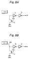
- Figs, 7A and 7B which illustrate an example of the mode setting circuit of Figs. 1, 3 and 5
- two inverters I1 and I2 in series are manufactured on a semiconductor chip in advance. Then, in a wiring forming step, if a wiring pattern is formed between an input of the inverter I1 and a ground power supply terminal (pad) GND as shown in Fig. 7A, the mode signal M is fixed at "0" (low level). Also, if a wiring pattern is formed between the input of the inverter I1 and a power supply terminal (pad) V cc as shown in Fig. 7B, the mode signal M is fixed at "1" (high level).
- Figs, 8A and 8B which illustrate another example of the mode setting circuit of Figs. 1, 3 and 5, two inverters I3 and I4 in series and a MOS transistor Q are manufactured on a semiconductor chip in advance. Then, in a bonding step, no bonding wiring is performed as shown in Fig. 8A, so the mode signal M is fixed at "0" (low level). Also, since a bonding wiring BW is performed as shown in Fig. 8B, the mode signal M is fixed at "1" (high level).
- Fig. 9 which illustrates an example of the tri-state buffer such as 402 of Figs. 1, 3 and 5
- P-channel MOS transistors 901 and 902 and N-channel MOS transistors 903 and 904 are connected in series between a V cc power supply line and a GND line.
- the gate of the P-channel transistor 901 is controlled via an inverter 905 by a control signal C
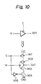
- Fig. 10 which illustrates an example of the tri-state buffer such as 59' of Figs. 3 and 5
- a burst counter 4-A includes inverters 404, 414, ⁇ , 485 in addition to the elements of the burst counter 4 of Figs. 3 and 4.
- the content of the burst counter 4-A is decremented by 1 as shown in Fig. 12. Therefore, the least significant bit A0' also has the largest transition frequency in the same way as in the burst counter 4 of Figs. 3 and 5, the burst counter 4 of Figs. 3 and 5 can be replaced by the burst counter 4-A of Fig. 11.
- a burst counter 4-B which has a burst length of 2 is provided instead of the burst counter 4 of Fig. 3 which has a burst length of 1.
- the second least significant bit A1' has the largest transition frequency. Therefore, the buffer 51 instead of the buffer 59 of Fig. 1 is connected to the OR circuit 9, in order to supply the second least significant bit A1' to the I/0 selection circuits 70 to 73 in a 4-bit I/0 configuration memory device mode.
- the tri-state buffer 59' is connected to the second least significant bit sides of the memory blocks 60 to 63, in order to supply the most significant bit A9' to the memory blocks 60 to 63 in a 4-bit I/0 configuration memory device mode. That is, in a 4-bit I/0 configuration memory device mode, the second least significant bit A1' serves as the most significant bit, and the most significant bit A9' serves as the second least significant bit. On the other hand, in an 8-bit I/0 configuration memory device mode, a tri-state buffer 51' is provided on the second least significant bit A1'.
- the N-th least significant bit A N-1 ' has the largest transition frequency. Therefore, in a 4-bit I/0 configuration memory device mode, the N-th least significart bit A N-1 ' is supplied to the I/0 selection circuits 70 to 73. Also, in a 4-bit I/0 configuration memory device mode, the most significant bit A9' is supplied to the memory blocks 60 to 63. That is, in a 4-bit I/0 configuration memory device mode, the N-th least significant bit A N-1 ' serves as the most significant bit, and the most significant bit A9' serves as the N-th least significant bit.
- a burst counter 4-C is constructed by a flip-flop 401', a tri-state buffer 402' an exclusive OR circuit 403' and an AND circuit 404' for the external address A0; a flip-folp 411', a tri-state buffer 412' an exclusive OR circuit 413' and an 4ND circuit 414' for the external address A1; ⁇ ; a flip-flop 481', a tri-state buffer 482' and an exclusive OR circuit 483' for the external address A8; and a flip-flop 491', a tri-state buffer 492' and an exclusive OR circuit 493' for the external address A9.
- the burst counter 4-C receives the synchronization clock signal SC, the content of the burst counter 4-C is counted down by 1, to generate a 9-bit internal address designated by A0', A1', ⁇ , A8' and A9' as shown in Fig. 16.
- the external address (A0, A1, ⁇ , A8, A9) (A0', A1', ⁇ , A8', A9') is 0000000000.
- a tri-state buffer 50" is provided instead of the buffer 50 and a tri-state buffer 59" is added, in order to supply the most significant bit A9' to the memory blocks 60 to 63 in an 8-bit I/0 configuration memory device mode. That is, in a 4-bit I/0 configuration memory device mode, the lower bits A0', A1', ⁇ , A8' are used for accessing the memory blocks 60 to 63 and the most significant bit A9'is used for controlling the I/0 selection circuits. On the other hand, in an 8-bit I/0 configuration memory device mode, the higher bits A1', A2', ⁇ , A9' are used for accessing the memory blocks 60 to 63.
- the two lower bits (A', A1') are changed from (0, 0) via (0, 1) and (1, 0) to (1, 1), from (0, 1) via (0, 0) and (1, 1) to (1, 0), from (1, 0) via (1, 1) and (0, 0) to (0, 1), or from (1, 1) via (1, 0) and (0, 1) to (0, 0).
- the power consumption in the memory section can be reduced to reduce the power consumption of the device.
Abstract
A synchronous semiconductor memory device has an M-bit I/O configuration memory device mode and an M×2k-bit I/O configuration memory device mode. In the former mode, n bits whose transition frequencies are smaller are selected from an m-bit internal address and are used to access a memory section (60∼63, 60'∼63'), while the other k (= m-n) bits whose transition frequencies are larger are selected from the m-bit internal address to select one of 2k groups of internal data lines (D₀∼D₇) of the memory section and connect them to some of data input/output pins (P₀∼P₃). In the latter mode, n bits whose transition frequencies are larger are selected from the m-bit internal address and are used to access the memory section, while the 2k groups of the data lines are connected to all the data input/output pins.
Description
- The present invention relates to a semiconductor memory device, and more particularly, to a synchronous semiconductor memory device where a plurality of input/output (I/O) bit configurations are manufactured on one chip and one of the I/O bit configurations is selected and fixed by a mode setting circuit determined at a wiring step or a similar manufacturing step.
- Recently, as the operation speed of microprocessors has increased, high speed access is also required for a main memory which is generally constructed by a dynamic random access memory (DRAM) device, for example. In order to satisfy this requirement, synchronous semiconductor memory devices have been developed.
- In a synchronous semiconductor memory device, when an external address as well as a data read/write command is supplied thereto, the external address is latched in a burst counter, so that a read/write operation is performed upon a memory section using this external address in the burst counter. Then, the content of the burst counter is incremented or decremented by receiving a synchronization clock signal, so that sequential read/write operations are performed upon the memory section using incremented or decremented addresses in the burst counter. Thus, in a synchronous semiconductor memory device, internal addresses are automatically generated inside of the device after an external address with a read/write command is received, and read/write operations are successively carried out by using the internal addresses, to thereby realize a high speed read/write operation based upon a burst operation.
- On the other hand, two kinds of semiconductor memory devices such as a 4-bit I/O configuration memory device and an 8-bit I/O configuration memory device are manufactured on one chip, and one of the memory devices is selected and fixed at a final stage such as a wiring step or a bonding step. That is, when such two kinds of memory devices are manufactured, most circuitry layouts thereof are commonly designed, to reduce the design cost. Also, the mode setting or fixing of the two memory devices is carried out at a later stage of the manufacturing steps, to rapidly comply with customers' orders.
- In a prior art synchronous semiconductor memory device in which two kinds of semiconductor devices such as an M-bit I/O configuration memory device and an M×2k-bit I/O configuration are manufactured on one chip, and one of the semiconductor devices is selected to be fixed at a later stage of the manufacturing steps, m-bit (m > k) internal addresses are successively generated, and lower n bits (n = m-k) of the m-bit internal addresses are used to access a memory section both in an M-bit I/O configuration memory device mode and in an M×2k-bit I/O configuration memory device mode. Then, only in the M-bit I/O configuration memory device mode, the other k bits of the m-bit internal addresses are used to select one of 2 k groups of data lines of the memory section and connect them to some of data input/output pins. Conversely, in the M×2k-bit I/O configuration memory device mode, all the data lines of the memory section are connected to all the data input/output pins regardless of the other k bits of the m-bit internal addresses. This will be explained later in detail.
- In the above-described prior art synchronous DRAM device, however, since the same lower n bits of the m-bit internal addresses are used to access the memory section in the M-bit I/O configuration memory device mode and in the M×2k-bit I/O configuration memory device mode, the frequency of transition of the lower n bits of the m-bit internal addresses is so large as to increase the power consumption in decoders, amplifiers and the like of the memory section in the M-bit I/O configuration memory device mode. This also will be explained later in detail.
- It is an object of the present invention to reduce the power consumption in a synchronous semiconductor memory device in which two or more kinds of I/O configuration semiconductor devices are manufactured on one chip, and one of the semiconductor devices is selected and fixed at a later stage of the manufacturing steps.
- According to the present invention, in the M-bit I/O configuration memory device mode, n bits whose transition frequencies are smaller are selected from the m-bit internal adresses and are used to access the memory section, while the other k (k = m-n) bits whose transition frequencies are larger are selected from the m-bit internal adresses to select one of the 2k groups of the internal data lines and connect them to some of the data input/output pins. Contrary to this, in the M×2 k-bit I/O configuration memory device mode, n bits whose transition frequencies are larger are slected from the m-bit internal addresses and are used to access the memory section, while the 2k groups of the data lines are connected to all the data input/output pins.
- Thus, since the n bits of the m-bit internal addresses for accessing the memory section in the M-bit I/O configuration memory device mode have small transition frequencies, the power consumption in decoders, amplifiers and the like of the memory section is reduced to reduce the power consumption in the device.
- The present invention will be more clearly understood from the description as set forth below, as compared with the prior art, with reference to the accompanying drawings, wherein:
- Fig. 1 is a circuit diagram illustrating a prior art synchronous semiconductor memory device;
- Fig. 2 is a table showing examples of the internal accresses of the device of Fig. 1;
- Fig. 3 is a circuit diagram illustrating a first embodiment of the synchroous semiconductor memory device according to the present invention;
- Fig. 4 is a partial circuit diagram illustrating a modification of the device of Fig. 3;
- Fig. 5 is a circuit diagram illustrating a second embodiment of the synchroous semiconductor memory device according to the present invention;
- Fig. 6 is a partial detailed circuit diagram of the device of Fig. 5;
- Figs. 7A and 7B are circuit diagrams of an example of the mode setting circuit of Figs. 1, 3 and 5;
- Figs. 8A and 8B are circuit diagrams of another example of the mode setting circuit of Figs. 1, 3 and 5;
- Fig. 9 is a circuit diagram of the tri-state buffer of Figs. 1, 3 and 5;
- Fig. 10 is a circuit diagram of the tri-state buffer of Figs. 3 and 5;
- Fig. 11 is a circuit diagram of a modification of the burst counter of Figs. 3 and 5;
- Fig. 12 is a table showing examples of the internal addresses of the burst counter of Fig. 11;
- Fig. 13 is a circuit diagram illustrating a third embodiment of the synchronous semiconductor memory device according to the present invention;
- Fig. 14 is a table showing examples of the internal addresses of the burst counter of Fig. 13;
- Fig. 15 is a circuit diagram illustrating a fourth embodiment of the synchronous semiconductor memory device according to the present invention; and
- Fig. 16 is a table showing examples of the internal addresses of the burst counter of Fig. 15.
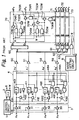
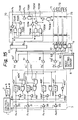
- Before the description of the preferred embodiments, a prior art synchronous semiconductor memory device will be explained with reference to Figs. 1 and 2.
- In Fig. 1, a 4-bit I/O configuration memory device and an 8-bit I/O configuration memory device are manufactured on one chip, and one of the devices is selected and fixed at a wiring step or the like.
-
Reference numeral 1 designates a control circuit for generating a latch clock signal LC, a synchronization clock signal SC, and the like. Also, thecontrol circuit 1 controls a flip-flop 2. That is, in a read mode, the flip-flop 2 is set, so that a read signal R is made high (="1") and a write signal W is made low (="0"). Contrary to this, in a write mode, the flip-flop 2 is reset, so that the read signal R is made low (="0") and a write signal W is made high (="1"). - A
latch circuit 3 recieves the latch control signal LC to latch a 10-bit external address designated by A₀, A₁, ···, A₈ and A₉. The latch circuit is constructed by tri-statebuffers latch circuit 3 is supplied to aburst counter 4. - The
burst counter 4 is constructed by a flip-flop 401, a tri-statebuffer 402 and aninverter 403 for the external address bit A₀; a flip-flop 411, a tri-statebuffer 412 and aninverter 413 for the external address bit A₁; ···; a flip-flop 481, a tri-statebuffer 482, an exclusive ORcircuit 483 and anAND circuit 484 for the external address bit A₈; and a flip-flop 491, a tri-statebuffer 492, an exclusive ORcircuit 493 and anAND circuit 494 for the external address bit A₉. As a result, every time theburst counter 4 receives the synchronization clock signal SC, the content of theburst counter 4 is counted up by +1, to generate a 9-bit internal address designated by A₀', A₁',···, A₈' and A₉' as shown in Fig. 2. In Fig. 2, note that the external address (A₀, A₁,···, A₈, A₉) = (A₀', A₁',···, A₈', A₉') is 0000000000. - The internal address bits A₀', A₁', ···, A₈', A₉' are supplied to
buffers memory blocks - Each of the memory blocks 60, 61, 62 and 63 decodes the 9 bits A₀', A₁',···, A₈' of the internal address. As a result, in a read mode (R = "1"), two memory cell data an each memory block 60 (61, 62, 63) are amplified and are output to internal data lines D₀ and D₄ (D₁, D₅; D₂, D₆; and D₃, D₇). Contrary to this, in a write mode (W = "1"), data on the internal data lines D₀ and D₄ (D₁, D₅; D₂, D₆; and D₃, D₇) are written into two memory cells of each of the memory blocks 60, 61, 62 and 63.
- The internal data lines D₀ D₄ D₁, D₅, D₂, D₆, D₃and D₇ correspond to data input/output pins P₀, P₄, P₁, P₅, P₂, P₆, P₃ and P₇, respectively. Also, input/output (I/O)
selection circuits D ₃ and D₇ and the data I/O pins P₀, P₄, P₁, P₅, P₂, P₆, P₃ and P₇. That is, in a 4-bit I/O configuration memory device mode, only the data input/output pins P₀ and P₃ are made effective. Therefore, in this case, the I/O selection circuits 70 to 73 are activated, so that either the internal data lines D₀ to D₃ or the internal data lines D₄ to D₇ are selected and are connected to the data input/output pins P₀ to P₃. On the other hand, in an 8-bit I/O configuration memory device mode, all the data input/output pins P₀ to P₇ are made effective. Therefore, in this case, the I/O selection circuits 70 to 73 are deactivated, i.e., the I/O selection circuits 70 to 73 are in a through state, so that the internal data lines D₀ to D₇ are connected to the data input/output pins P₀ to P₇, respectively. - The I/
O selection circuit 70 is constructed bytri-state buffers gate circuits tri-state buffers gate circuits O selection circuits O selection circuit 70. - The I/
O selection circuits mode setting circuit 8 and the most significant bit A₉' of the internal address in addition to the read signal R and the write signal W. That is, the mode signal M is supplied to thegate circuits circuit 9 to thegate circuits - In a 4-bit I/O configuration memory device mode, the
mode setting circuit 8 causes the mode signal M to be "0". As a result, the outputs of thegate circuits O selection circuits 70 to 73 become "0", so that thetri-state buffers D ₃ or the internal data lines D₄ to D₇ are selected and are connected to a special group of the data input/output pins such as P₀ to P₃. In this case, the most significant bit A₉' is supplied via the ORcircuit 9 to thegate circuits tri-state buffer tri-state buffer D ₇ are connected to the data input/output pins P₀ to P₃, respectively. Thus, the I/O selection circuits 70 to 73 are placed in an activated state, i.e., in a selection state by the most significant bit A₉'. - In an 8-bit I/O configuration memory device mode, the
mode setting circuit 8 causes the mode signal M to be "1". As a result, the output of theOR circuit 9 becomes "1" regardless of the most significant bit A₉', so that thegate circuits O selection circuits 70 to 73 are activated, thus connecting the internal data lines D₀ to D₃ to the data input/output pins P₀ to P₃, respectively. Simultaneously, the outputs of thegate circuits O selection circuits 70 to 73 become "1", so that thetri-state buffers O selection circuits 70 to 71 are a in deactivated state, i.e., in a nonselection state by the most significant bit A₉', so that the internal data lines D₀ to D₇ are connected to the data input output pins P₀ to P₇, respectively. - In the device of Fig. 1, however, since the leust significant bit A₀' of the internal address which has a large transistion frequency is used to access the memory section formed by the memory blocks 60, 61, 62 and 63, the power consumption in the decoders, the amplifiers and the like thereof is increased.
- In Fig. 3, which illustrates a first embodiment of the present invention, the
buffer 50 instead of thebuffer 59 of Fig. 1 is connected to theOR circuit 9, in order to supply the least significant bit A₀' to the I/O selection circuits 70 to 73 in a 4-bit I/O configuration memory device mode. Also, a tri-state buffer 59' is provided instead of thebuffer 59 of Fig. 1 and is connected to the least significant bit sides of the memory blocks 60 to 63, in order to supply the most significant bit A₉' to the memory bolcks 60 to 63 in a 4-bit I/O configuration memory device mode. That is, in a 4-bit I/O configuration memory device mode, the least significant bit A₀' serves as the most significant bit, and the most significant bit A₉' serves as the least significant bit. On the other hand, in an 8-bit I/O configuration memory device mode, a tri-state buffer 50' is provided on the least significant bit A₀'. - In a 4-bit I/O configuration memory device mode, the
mode setting circuit 8 causes the mode signal M to be "0". As a result, the tri-state buffer 50' is deactivated and the tri-state buffer 59' is activated Therefore, the most significant bit A₉' instead of the least significant bit A₀' is supplied to the memory blocks 60 to 63, so that each of the memory blocks 60 to 63 is accessed by internal addresses designated by the mine bits A₉', A₁',··· , and A₈'. Such internal addresses have a transition frequency depending upon every two synchronization clock signals SC as shown in Fig. 2. Therefore, the power consumption in the memory blocks 60 to 63 is reduced as compared with that in Fig. 1. - Also, simultaneously, the outputs of the
gate circuits O selection circuits 70 to 73 become "0", so that thetri-state buffers circuit 9 to thegate circuits tri-state buffer tri-state buffer O selection circuits 70 to 73 are placed in an activated state, i.e., in a selection state by the least significant bit A₀'. - In an 8-bit I/O configuration memory device mode, the
mode setting circuit 8 causes the mode signal M to be "1". As a result, the tri-state buffer 50' is activated while the tri-state buffer 59' is deactivated. Therefore, each of the memory blocks 60 to 63 is accessed by the lower bits A₀', A₁', ···, and A₈' of the internal addresses in the same way as in the device of Fig. 1. Also, the output of theOR circuit 9 becomes "1" regardless of the least significant bit A₀', so that thegate circuits O selection circuits 70 to 73 are activated, thus connecting the internal data lines D₀ to D₃ to the data input/output pins P₀ to P₃, respectively. Simultaneously, the outpus of thegate circuits O selection circuits 70 to 73 become "1", so that thetri-state buffers O selection circuits 70 to 71 are in a deactivated state, i.e., in a nonselection state by the least significant bit A₉', so that the internal data lines D₀ to D₇ are connected to the data input output pins P₀ to P₇, respectively. - Thus, according to the first embodiment, in a 4-bit I/O configuration memory device mode, the least significant bit A₀' is exchanged with the most significant bit A₉'. That is, the least significant bit A₀' which has the largest transition frequency is used for controlling the I/
O selection circuits 70 to 73, while the most significant bit A₉' while has the smallest transition frequency is used for accessing the memory blocks 60 to 63. Thus, the power consumption in the decorders, the amplifiers and the like of the memory blocks 60 to 63 can be reduced. - In Fig. 4, which illustrates a modification of the device of Fig. 3, the
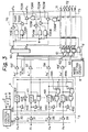
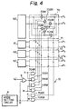
gate circuits O control circuit 10 are provided commonly for the I/O selection circuits 70 to 73, thus reducing the circuitry elements. - In Fig. 5, which illustrates a second embodiment of the present invention, a 4-bit I/O configuration memory device and a 16-bit I/O configuration memory device are manufactured on one chip, and one of the devices is selected and fixed at a wiring step or the like. In this case, a memory block 60' has internal data lines D₀, D₄, D₈ and D₁₂, a memory block 61' has internal data lines D₁, D₅, D₉ and D₁₃, a memory block 62' has internal data lines D₂, D₆, D₁₀ and D₁₄, and a memory block 60' has internal data lines D₃, D₇, D₁₁ and D₁₅. That is, four groups of the internal data lines D₀ to D₃, D₄ to D₇, D₈ to D₁₁, and D₁₂ to D₁₅ are provided. Similarly, an I/O selection circuit 70' has data input/output pins P₀, P₄, P₈ and P₁₂, an I/O selection circuit 71' has data input/output pins P₁, P₅, P₉ and P₁₃ , an I/O selection circuit 72' has data input/output pins P₂, P₆, P₁₀ and P₁₄, and an I/O selection circuit 73' has data input/output pins P₃, P₇, P₁₁ and P₁₅. That is, four groups of the data input/output pins P₀ to P₃, P₄ to P₇,
P ₈ to P₁₁, and P₁₂ to P₁₅ are provided. That is, in a 4-bit I/O configuration memory device mode, only the data input/output pins P₀ and P₃ are made effective.
Therefore, in this case, the I/O selection circuits 70' to 73' are activated, so that one group of the internal data lines D₀ and D₃, the internal data lines D₄ to D₇ the internal data lines D₈ to D₁₁, and the internal data lines D₁₂ to D₁₅ are selected and are connected to the data input/output pins P₀ to P₃. On the other hand, in a 16-bit I/O configuration memory device mode, all the data input/output pins P₀ to P₁₅ are mode effective. Therefore, in this case, the I/O selection circuits 70' to 73' are deactivated, i.e., the I/O selection circuits 70' to 73' are in a through state, so that the internal data lines that the internal data lines D₀ to D₁₅ are connected to the data input/output pins P₀ to P₁₅, respectively. Such a connection is carried out by the I/O selection circuits 70' to 73' which are also controlled by an I/O control circuit 10'. - In Fig. 5, the
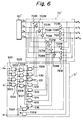
buffers buffers - In Fig. 6, which is a detailed circuit of the I/O selection circuit 70' and the I/O control circuit 10' of Fig. 5, the I/
O slection circuit 70 is constructed bytri-state buffers 701R to 703R and 707R to 710R operated in a read mode (R = "1"), andtri-state buffers 701W to 703W and 707W to 710W operated in a write mode (W = "1"). Also, the I/O control circuit 10' is constructed bygate circuits 1001 to 1004 for decoding the lower bits A₀' and A₁',gate circuits 1005 to 1008 controlled by the mode signal M,gate circuits 1009 to 1012 controlled by the read signal R, andgate circuits 1013 to 1016 controlled by the write signal W. - In a 4-bit I/O configuration memory device mode, the
mode setting circuit 8 causes the mode signal M to be "0". As a result, the tri-state buffers 50' and 51' are deactivated and the tri-state buffers 58' and 59' are activated. Therefore, the higher bits A₈' and A₉' instead of the lower bits A₀'and A₁' are supplied to the memory blocks 60' to 63', so that each of the memory blocks 60' to 63' is accessed by internal addresses designated by the eight bits A₈', A₉', A₃',···. Such internal addresses have a transition frequency depending upon every four synchronization clock signals SC as shown in Fig. 2. Therefore, the power consumption in the memory blocks 60 to 63 is reduced. - Also, simultaneously, the outputs of the
gate circuits tri-state buffers gate circuits 1001 to 1004 of the decoder of the I/O control circuit 10'. - If Ao' = "1" and A₁' = "1", the output of the
gate circuit 1001 is "1". In this case, since M = "0", any of the decoding outputs of thegate circuits 1001 to 1004 can pass through thegate circuits 1005 to 1008. Therefore, the output of thegate circuit 1001 passes through thegate circuit 1005 and reaches thegate circuits tri-state buffer - Also,if A₀' = "0" and A₁' = "1", the output of the
gate circuit 1002 is "1". Therefore, the output of thegate circuit 1002 passes through thegate circuit 1006 and reaches thegate circuits tri-state buffer - Further, if Ao' = "1" and A₁' = "0", the output of the
gate circuit 1003 is "1". Therefore, the output of thegate circuit 1003 passes through thegate circuit 1007 and reaches thegate circuits tri-state buffer - Still further, if Ao' = "0" and A₁' = "0", the output of the
gate circuit 1004 is "1". Therefore, the output of thegate circuit 1004 passes through thegate circuit 1008 and reaches thegate circuits tri-state buffer - In a 16-bit I/0 configuration memory device mode,the
mode setting circuit 8 causes the mode signal M to be "1". As a result, the tri-state buffer 50' and 51' are activated while the tri-state buffers 58' and 59' are deactivated. Therefore, each of the memory blocks 60' to 63' is accessed by the eight lower bits A₀', A₁',···, and A₇' of the internal addresses. - Also, simultaneously, the output of the
gate circuit 1005 becomes "1" and the outputs of thegate circuits 1006 to 1008 become "0" regardless of the lower bits A₀'and A₁'. Therefore, thetri-state buffer gate circuit gate circuit tri-state buffers tri-state buffers - Thus, according to the second embodiment, in a 4-bit I/0 configuration memory device mode, the lower bits A₀' and A₁' are exchanged with the higher bits A₈' and A₉'. That is, the lower bits A₀' and A₁' which have larger transition frequency are used for controlling the I/0 selection circuits 70' to 73', while the higher bits A₈' and A₉' which have smaller transition frequency are used for accessing the memory blocks 60' to 63'. Thus, the power consumption in the decoders, the amplifiers and the like of the memory blocks 60' to 63' can be reduced.
- In Figs, 7A and 7B, which illustrate an example of the mode setting circuit of Figs. 1, 3 and 5, two inverters I₁ and I₂ in series are manufactured on a semiconductor chip in advance. Then, in a wiring forming step, if a wiring pattern is formed between an input of the inverter I₁ and a ground power supply terminal (pad) GND as shown in Fig. 7A, the mode signal M is fixed at "0" (low level). Also, if a wiring pattern is formed between the input of the inverter I₁ and a power supply terminal (pad) V cc as shown in Fig. 7B, the mode signal M is fixed at "1" (high level).
- In Figs, 8A and 8B, which illustrate another example of the mode setting circuit of Figs. 1, 3 and 5, two inverters I₃ and I₄ in series and a MOS transistor Q are manufactured on a semiconductor chip in advance. Then, in a bonding step, no bonding wiring is performed as shown in Fig. 8A, so the mode signal M is fixed at "0" (low level). Also, since a bonding wiring BW is performed as shown in Fig. 8B, the mode signal M is fixed at "1" (high level).
- In Fig. 9, which illustrates an example of the tri-state buffer such as 402 of Figs. 1, 3 and 5, P-
channel MOS transistors channel MOS transistors channel transistor 901 is controlled via aninverter 905 by a control signal C, and the gate of the N-channel transistor 904 is controlled directly by the control signal C. Therefore, when C = "0", the tri-state buffer is in a high impedance state, while, when C = "1", an output signal OUT is an inverted signal of an input signal IN. - In Fig. 10, which illustrates an example of the tri-state buffer such as 59' of Figs. 3 and 5, the
inverter 905 of Fig. 9 is connected to the gate of the N-channel transistor 904. Therefore, when C = "1", the tri-state buffer is in a high impedance state, while, when C = "0", an output signal OUT is an inverted signal of an input signal IN. - In Fig, 11, which is a modification of the
burst counter 4 of Figs. 3 and 5, a burst counter 4-A includesinverters burst counter 4 of Figs. 3 and 4. In this case, when the synchronization clock signal SC is received by the burst counter 4-A, the content of the burst counter 4-A is decremented by 1 as shown in Fig. 12. Therefore, the least significant bit A₀' also has the largest transition frequency in the same way as in theburst counter 4 of Figs. 3 and 5, theburst counter 4 of Figs. 3 and 5 can be replaced by the burst counter 4-A of Fig. 11. - In Fig. 13, which illustrates a third embodiment of the present invention, a burst counter 4-B which has a burst length of 2 is provided instead of the
burst counter 4 of Fig. 3 which has a burst length of 1. In this case, as shown in Fig. 14, which shows the content of the burst counter 4-B, the second least significant bit A₁' has the largest transition frequency. Therefore, thebuffer 51 instead of thebuffer 59 of Fig. 1 is connected to theOR circuit 9, in order to supply the second least significant bit A₁' to the I/0selection circuits 70 to 73 in a 4-bit I/0 configuration memory device mode. Also, the tri-state buffer 59' is connected to the second least significant bit sides of the memory blocks 60 to 63, in order to supply the most significant bit A₉' to the memory blocks 60 to 63 in a 4-bit I/0 configuration memory device mode. That is, in a 4-bit I/0 configuration memory device mode, the second least significant bit A₁' serves as the most significant bit, and the most significant bit A₉' serves as the second least significant bit. On the other hand, in an 8-bit I/0 configuration memory device mode, a tri-state buffer 51' is provided on the second least significant bit A₁'. - Generally, in Fig. 3, if the burst counter has a burst length of 2N (N = 1, 2, ···), the N-th least significant bit A N-1' has the largest transition frequency. Therefore, in a 4-bit I/0 configuration memory device mode, the N-th least significart bit AN-1' is supplied to the I/0
selection circuits 70 to 73. Also, in a 4-bit I/0 configuration memory device mode, the most significant bit A₉' is supplied to the memory blocks 60 to 63. That is, in a 4-bit I/0 configuration memory device mode, the N-th least significant bit A N-1' serves as the most significant bit, and the most significant bit A₉' serves as the N-th least significant bit. - In Fig. 15, which illustrates a fourth embodiment of the present invention, a burst counter 4-C is constructed by a flip-flop 401', a tri-state buffer 402' an exclusive OR circuit 403' and an AND circuit 404' for the external address A₀; a flip-folp 411', a tri-state buffer 412' an exclusive OR circuit 413' and an 4ND circuit 414' for the external address A₁; ···; a flip-flop 481', a tri-state buffer 482' and an exclusive OR circuit 483' for the external address A₈; and a flip-flop 491', a tri-state buffer 492' and an exclusive OR circuit 493' for the external address A₉. As a result, every time the burst counter 4-C receives the synchronization clock signal SC, the content of the burst counter 4-C is counted down by 1, to generate a 9-bit internal address designated by A₀', A₁', ···, A₈' and A₉' as shown in Fig. 16. In Fig. 16, note that the external address (A₀, A₁,··· , A₈, A₉) = (A₀', A₁',···, A₈', A₉') is 0000000000.
- As shown in Fig. 16, the most significant bit A₉' has the largest transition frequency. Therefore, a
tri-state buffer 50" is provided instead of thebuffer 50 and atri-state buffer 59" is added, in order to supply the most significant bit A₉' to the memory blocks 60 to 63 in an 8-bit I/0 configuration memory device mode. That is, in a 4-bit I/0 configuration memory device mode, the lower bits A₀', A₁',···, A₈' are used for accessing the memory blocks 60 to 63 and the most significant bit A₉'is used for controlling the I/0 selection circuits. On the other hand, in an 8-bit I/0 configuration memory device mode, the higher bits A₁', A₂', ···, A₉' are used for accessing the memory blocks 60 to 63. - Note that the present invention can be generally applied to a synchronous semiconductor memory device where an M (M = 1, 2, ···)-bit I/0 configuration memory device and an M×2k (k = 1,2, ···)-bit I/0 configuration memory device are manufactured on one chip and one of the devices is selected and fixed at a wiring forming step or a bonding step. Also, the present invention can be applied to an interleave mode. In the interleave mode, for example, if the burst length is 4, the two lower bits (A', A₁') are changed from (0, 0) via (0, 1) and (1, 0) to (1, 1), from (0, 1) via (0, 0) and (1, 1) to (1, 0), from (1, 0) via (1, 1) and (0, 0) to (0, 1), or from (1, 1) via (1, 0) and (0, 1) to (0, 0).
- As explained hereinbefore, according to the present invention, since the memory section is accessed by some bits of internal addresses having a smaller transition frequency, the power consumption in the memory section can be reduced to reduce the power consumption of the device.
Claims (13)
- A synchronous semiconductor device comprising:
an internal address generating means (3, 4, 4-A, 4-B) for generating an m(m=2, 3,···)-bit internal address which is successively changed;
a memory section (60∼63, 60'∼63') accessed by n(n<m) bits and having 2m-n groups of internal data lines (D₀∼D₃, D₄∼D₇; D₀∼D₃, D₄∼D₇, D ₈∼D₁₁, D₁₂∼D₁₅);
2m-n groups of data input/output pins (P₀ ∼P₃, P₄∼P₇; P₀∼P₃, P₄∼P₇, P₈∼P₁₁, P₁₂∼P₁₅);
M (M = 1, 2, ···)-bit input/output configuration memory device mode setting means (8, 70, ··· , 70') for accessing said memory section by n bits of said m-bit internal address having smaller transition frequencies and for selecting one group of said 2m-n groups of internal data lines by (m-n) bits of said m-bit internal address having larger transition frequencies to connect said selected group of internal data lines to one group of said 2m-n groups of data input/output pins (P₀ ∼P₃); and
M×2m-n-bit input/output configuration memory device mode setting means (8, 70,···, 70') for accessing said memory section by n bits of said m-bit internal address having larger transition frequencies and for connecting said 2m-n groups of internal data lines to said 2m-n groups of data input/output pins. - A device as set forth in claim 1, wherein said internal address generating means receives a synchronization clock signal (SC) to increment said m-bit internal address by 1,
said n bits of said m-bit internal address having smaller transition frequencies being higher n bits of said m-bit internal address,
said (m-n) bits of said m-bit internal address having larger transition frequencies being lower (m-n) bits of said m-bit internal address,
said n bits of said m-bit internal address having larger transition frequencies being lower n bits of said m-bit internal address. - A device as set forth in claim 1, wherein said internal address generating means receives a synchronization clock signal (SC) to decrement said m-bit internal address by 1,
said n bits of said m-bit internal address having smaller transition frequencies being higher n bits of said m-bit internal address,
said (m-n) bits of said m-bit internal address having larger transition frequencies being lower (m-n) bits of said m-bit internal address,
said n bits of said m-bit internal address having larger transition frequencies being lower n bits of said m-bit internal address. - A device as set forth in claim 1, wherein said internal address generating means receives a synchronization clock signal (SC) to increment said m-bit internal address by 2,
said n bits of said m-bit internal address having smaller transition frequencies being higher n bits of said m-bit internal address, and the least significant bit thereof,
said (m-n) bits of said m-bit internal address having larger transition frequencies being lower (m-n) bits of said m-bit internal address except for the least significant bit thereof,
said n bits of said m-bit internal address having larger transition frequencies being lower n bits of said m-bit internal address, - A device as set forth in claim 1, wherein said internal address generating means receives a synchronization clock signal (SC) to decrement said m-bit internal address by 2,
said n bits of said m-bit internal address having smaller transition frequencies being higher n bits of said m-bit internal address and the least significant bit thereof,
said (m-n) bits of said m-bit internal address having larger transition frequencies being lower (m-n) bits of said m-bit internal address except for the least significant bit thereof,
said n bits of said m-bit internal address having larger transition frequencies being lower n bits of said m-bit internal address, - A device as set forth in claim 1, wherein said internal address generating means receives a synchronization clock signal (SC) to increment said m-bit internal address by 2N-1(N = 3, 4, ···),
said n bits of said m-bit internal address having smaller transition frequencies being higher n bits of said m-bit internal address and the least significant bits to the N-th least significant bits thereof,
said (m-n) bits of said m-bit internal address having larger transition frequencies being lower (m-n) bits of said m-bit internal address except for the least significant bits to the N-th least significant bits thereof,
said n bits of said m-bit internal address having larger transition frequencies being lower n bits of said m-bit internal address, - A device as set forth in claim 1, wherein said internal address generating means receives a synchronization clock signal (SC) to decrement said m-bit internal address by 2N-1(N = 3, 4, ···),
said n bits of said m-bit internal address having smaller transition frequencies being higher n bits of said m-bit internal address and the least significant bits to the N-th least significant bits thereof,
said (m-n) bits of said m-bit internal address having larger transition frequencies being lower (m-n) bits of said m-bit internal address except for the least significant bits to the N-th least significant bits thereof,
said n bits of said m-bit internal address having larger transition frequencies being lower n bits of said m-bit internal address, - A device as set forth in claim 1, wherein said internal address generating means receives a synchronization clock signal (SC) to change said m-bit internal address so that higher bits of said m-bit internal address have larger transition frequencies than lower bits of said m-bit internal address;
said n bits of said m-bit internal address having smaller transition frequencies being lower n bits of said m-bit internal address,
said (m-n) bits of said m-bit internal address having larger transition frequencies being higher (m-n) bits of said m-bit internal address,
said n bits of said m-bit internal address having larger transition frequencies being lower n bits of said m-bit internal address. - A synchronous semiconductor device comprising:
an internal address generating means (3, 4, 4-A, 4-B) for generating an m (m=2, 3, ···)-bit internal address which is successively changed;
a memory section (60∼63, 60'∼63') accessed by n(n<m) bits and having 2m-n groups of internal data lines (D₀∼D₃, D₄∼D₇; D₀∼D₃, D₄∼D₇, D ₈∼D₁₁, D₁₂∼D₁₅);
2m-n groups of data input/output pins (P₀ ∼P₃, P₄∼P₇; P₀∼P₃, P₄∼P₇, P₈∼P₁₁, P₁₂∼P₁₅);
M (M = 1, 2, ···)-bit input/output configuration memory device mode setting means (8, 70, ··· , 70') for accessing said memory section by higher n bits of said m-bit internal address and for selecting one group of said 2m-n groups of internal data lines by lower (m-n) bits of said m-bit internal address to connect said selected group of internal data lines to one group of said 2m-n groups of data input/output pins (P₀ ∼P₃); and
M×2m-n-bit input/output configuration memory device mode setting means (8, 70,···, 70') for accessing said memory section by lower n bits of said m-bit internal address and for connecting said 2m-n groups of internal data lines to said 2m-n groups of data input/output pins. - A synchronous semiconductor device comprising:
an internal address generating means (3, 4, 4-A, 4-B) for generating an m (m=2, 3, ···)-bit internal address which is successively changed;
a memory section (60∼63, 60'∼63') accessed by n (n<m) bits and having 2m-n groups of internal data lines (D₀∼D₃, D₄∼D₇; D₀∼D₃, D₄∼D₇, D ₈∼D₁₁, D₁₂∼D₁₅);
2m-n groups of data input/output pins (P₀ ∼P₃, P₄∼P₇; P₀∼P₃, P₄∼P₇, P₈∼P₁₁, P₁₂∼P₁₅);
M (M = 1, 2, ···)-bit input/output configuration memory device mode setting means (8, 70, ··· , 70') for accessing said memory section by lower n bits of said m-bit internal address and for selecting one group of said 2m-n groups of internal data lines by higher (m-n) bits of said m-bit internal address to connect said selected group of internal data lines to one group of said 2m-n groups of data input/output pins (P₀ ∼P₃); and
M×2m-n-bit input/output configuration memory device mode setting means (8, 70,···, 70') for accessing said memory section by higher n bits of said m-bit internal address and for connecting said 2 m-n groups of internal data lines to said 2m-n groups of data input/output pins. - A synchronous semiconductor memory device comprising:
an external address latch circuit (3) for receiving a latch signal (LC) to latch an m-bit external address (A₀, A₁,···, A₉);
a burst counter (4, 4-A, 4-B, 4-C), connected to said external address latch circuit, for receiving a synchronization clock signal (SC) to generate an m-bit internal address (A₀', A₁', ···, A₉') based upon said external address;
a memory section (60∼63, 60'∼63') accessed by n (n < m) bits and having 2m-n groups of internal data lines (D₀∼D₃, D₄∼D₇; D₀∼D₃, D₄∼D₇, D₈∼ D₁₁, D₁₂∼D₁₅);
2m-n groups of data input/output pins (P₀∼ P₃, P₄∼O₇; P₀∼P₃, P₄∼P₇, P₈∼P₁₁, P₁₂∼P₁₅);
an input/output selection means (70∼73, 70'∼73'), connected between said 2m-n groups of internal data lines and said 2m-n groups of data input/output pins, for selecting one group of said 2m-n groups of internal data lines for one of said 2m-n groups of data input/output pins in an M (M = 1, 2, ···)-bit input/output configuration memory device mode and for connecting said 2m-n groups of internal data lines to said 2m-n groups of data input/output pins in an M×2m-n-bit input/output configuration memory device mode;
M (M = 1, 2, ···)-bit input/output configuration memory device mode setting means (8, 70, ··· , 70') for accessing said memory section by n bits of said m-bit internal address having smaller transition frequencies and for activating said input/output selection means by supplying (m-n) bits of said m-bit internal address having larger transition frequencies; and
M×2m-n-bit input/output configuration memory device mode setting means (8, 70,···, 70') for accessing said memory section by n bits of said m-bit internal address having larger transition frequencies and for deactivating said input/output selection means to connect said 2m-n groups of internal data lines to said 2m-n groups of data input/output pins. - A device as set forth in claim 10, wherein said burst counter receives a synchronization clock signal (SC) to change said m-bit internal address by 2N-1 (N = 2, 3, ···),
said n bits of said m-bit internal address having smaller transition frequencies being higher n bits of said m-bit internal address and the least significant bits to the N-th least significant bits thereof,
said (m-n) bits of said m-bit internal address having larger transition frequencies being lower (m-n) bits of said m-bit internal address except for the least significant bits to the N-th least significant bits thereof,
said n bits of said m-bit internal address having larger transition frequencies being lower n bits of said m-bit internal address. - A synchronous semiconductor memory device comprising:
an internal address generating means (4, 4-A, 4-B, 4-C) for generating an m-bit internal address in response to a synchronization clock signal (SC);
a memory section (60∼63, 60'∼63') having 2k groups of internal data lines (D₀∼D₃, D₄∼ D₇), said memory section being capable of operating an M-bit input/output configuration memory device mode and an M×2k (k = 1, 2,···)-bit input/output configuration memory device mode,
said 2k groups of internal data lines selected by k bits of said m-bit internal address which bits are changed at a high frequency in response to said synchronization clock signal under said M-bit input/output configuration memory mode being equivalent to said 2k groups of internal data lines under said M× 2k-bit input/output configuration memory mode.
Applications Claiming Priority (2)
| Application Number | Priority Date | Filing Date | Title |
|---|---|---|---|
| JP212082/94 | 1994-08-12 | ||
| JP6212082A JPH0855471A (en) | 1994-08-12 | 1994-08-12 | Synchronous semiconductor memory device |
Publications (2)
| Publication Number | Publication Date |
|---|---|
| EP0696801A2 true EP0696801A2 (en) | 1996-02-14 |
| EP0696801A3 EP0696801A3 (en) | 1998-09-23 |
Family
ID=16616577
Family Applications (1)
| Application Number | Title | Priority Date | Filing Date |
|---|---|---|---|
| EP95112606A Withdrawn EP0696801A3 (en) | 1994-08-12 | 1995-08-10 | Synchronous semiconductor memory device with low power consumption |
Country Status (5)
| Country | Link |
|---|---|
| US (1) | US5608686A (en) |
| EP (1) | EP0696801A3 (en) |
| JP (1) | JPH0855471A (en) |
| KR (1) | KR0182303B1 (en) |
| CN (1) | CN1148249A (en) |
Cited By (1)
| Publication number | Priority date | Publication date | Assignee | Title |
|---|---|---|---|---|
| GB2296591A (en) * | 1994-12-31 | 1996-07-03 | Hyundai Electronics Ind | Data signal distribution circuit for synchronous memory |
Families Citing this family (7)
| Publication number | Priority date | Publication date | Assignee | Title |
|---|---|---|---|---|
| JP2991094B2 (en) * | 1995-09-19 | 1999-12-20 | 日本電気株式会社 | Semiconductor storage device |
| KR100431316B1 (en) * | 1997-06-27 | 2004-10-08 | 주식회사 하이닉스반도체 | DRAM PACKAGE FOR FORMING 1Mx16 I/O DRAM AND 2Mx8 I/O DRAM BY USING ONLY ONE PACKAGE, ADDRESS LINE THEREOF, AND METHOD FOR CHANGING WIDTHS OF ADDRESS LINE AND DATA LINE |
| US5973993A (en) | 1998-02-27 | 1999-10-26 | Micron Technology, Inc. | Semiconductor memory burst length count determination detector |
| US6766385B2 (en) | 2002-01-07 | 2004-07-20 | Intel Corporation | Device and method for maximizing performance on a memory interface with a variable number of channels |
| KR100892673B1 (en) * | 2007-09-05 | 2009-04-15 | 주식회사 하이닉스반도체 | Circuit for Replacing Address and Semiconductor Memory Apparatus with the Same |
| KR101581414B1 (en) * | 2009-02-05 | 2015-12-30 | 삼성전자주식회사 | Reconfigurable processor for reducing power consumption and method thereof |
| JP6068071B2 (en) * | 2012-09-14 | 2017-01-25 | ローム株式会社 | Load driving device and LED lighting apparatus using the same |
Family Cites Families (5)
| Publication number | Priority date | Publication date | Assignee | Title |
|---|---|---|---|---|
| EP0198429B1 (en) * | 1985-04-10 | 1991-07-24 | Nec Corporation | Word length selectable memory |
| JPS63188250A (en) * | 1987-01-30 | 1988-08-03 | Nec Corp | Memory circuit for optional word length |
| JP3992757B2 (en) * | 1991-04-23 | 2007-10-17 | テキサス インスツルメンツ インコーポレイテツド | A system that includes a memory synchronized with a microprocessor, and a data processor, a synchronous memory, a peripheral device and a system clock |
| JP2875476B2 (en) * | 1993-12-06 | 1999-03-31 | 松下電器産業株式会社 | Semiconductor memory device |
| JP2616567B2 (en) * | 1994-09-28 | 1997-06-04 | 日本電気株式会社 | Semiconductor storage device |
-
1994
- 1994-08-12 JP JP6212082A patent/JPH0855471A/en active Pending
-
1995
- 1995-08-08 US US08/512,420 patent/US5608686A/en not_active Expired - Lifetime
- 1995-08-10 EP EP95112606A patent/EP0696801A3/en not_active Withdrawn
- 1995-08-12 CN CN95116351A patent/CN1148249A/en active Pending
- 1995-08-12 KR KR1019950024877A patent/KR0182303B1/en not_active IP Right Cessation
Non-Patent Citations (1)
| Title |
|---|
| None |
Cited By (2)
| Publication number | Priority date | Publication date | Assignee | Title |
|---|---|---|---|---|
| GB2296591A (en) * | 1994-12-31 | 1996-07-03 | Hyundai Electronics Ind | Data signal distribution circuit for synchronous memory |
| GB2296591B (en) * | 1994-12-31 | 1998-09-09 | Hyundai Electronics Ind | Data signal distribution circuit for synchronous memory device |
Also Published As
| Publication number | Publication date |
|---|---|
| JPH0855471A (en) | 1996-02-27 |
| KR0182303B1 (en) | 1999-04-15 |
| EP0696801A3 (en) | 1998-09-23 |
| KR960008830A (en) | 1996-03-22 |
| US5608686A (en) | 1997-03-04 |
| CN1148249A (en) | 1997-04-23 |
Similar Documents
| Publication | Publication Date | Title |
|---|---|---|
| US4618947A (en) | Dynamic memory with improved address counter for serial modes | |
| US4044339A (en) | Block oriented random access memory | |
| US8284602B2 (en) | Pipe latch circuit of multi-bit prefetch-type semiconductor memory device with improved structure | |
| US6009494A (en) | Synchronous SRAMs having multiple chip select inputs and a standby chip enable input | |
| US6272053B1 (en) | Semiconductor device with common pin for address and data | |
| JPH04228174A (en) | Semiconductor memory | |
| EP0696801A2 (en) | Synchronous semiconductor memory device with low power consumption | |
| EP0249413B1 (en) | Semiconductor memory device | |
| EP0274378A2 (en) | Semiconductor memory device | |
| US5579264A (en) | Distributed signal drivers in arrayable devices | |
| JP3380828B2 (en) | Semiconductor memory device | |
| US7480776B2 (en) | Circuits and methods for providing variable data I/O width for semiconductor memory devices | |
| US6058448A (en) | Circuit for preventing bus contention | |
| US5446859A (en) | Register addressing control circuit including a decoder and an index register | |
| JPH09106678A (en) | Prefetch-type column decoder and semiconductor memory devicewith it | |
| US5363494A (en) | Bus interface circuit for connecting bus lines having different bit ranges | |
| EP0327950B1 (en) | Address modification circuit | |
| JPH0734184B2 (en) | Semiconductor device having chip select terminal pair | |
| US5983331A (en) | Semiconductor integrated circuit having a plurality of chips | |
| US4763304A (en) | Semiconductor random access memory device having switchable input and output bit forms | |
| US5524115A (en) | Input/output selection circuit of column repair | |
| US4514831A (en) | Static-type semiconductor memory device | |
| JP2663138B2 (en) | Semiconductor integrated circuit device | |
| JPH11242663A (en) | Memory capacitance switching method and semiconductor device for applying the same | |
| US7286424B2 (en) | Semiconductor integrated circuit device |
Legal Events
| Date | Code | Title | Description |
|---|---|---|---|
| PUAI | Public reference made under article 153(3) epc to a published international application that has entered the european phase |
Free format text: ORIGINAL CODE: 0009012 |
|
| AK | Designated contracting states |
Kind code of ref document: A2 Designated state(s): DE FR GB |
|
| PUAL | Search report despatched |
Free format text: ORIGINAL CODE: 0009013 |
|
| AK | Designated contracting states |
Kind code of ref document: A3 Designated state(s): DE FR GB |
|
| 17P | Request for examination filed |
Effective date: 19980810 |
|
| 17Q | First examination report despatched |
Effective date: 20000214 |
|
| STAA | Information on the status of an ep patent application or granted ep patent |
Free format text: STATUS: THE APPLICATION HAS BEEN WITHDRAWN |
|
| 18W | Application withdrawn |
Withdrawal date: 20001222 |