EP0689315A1 - Phase comparator - Google Patents
Phase comparator Download PDFInfo
- Publication number
- EP0689315A1 EP0689315A1 EP95401435A EP95401435A EP0689315A1 EP 0689315 A1 EP0689315 A1 EP 0689315A1 EP 95401435 A EP95401435 A EP 95401435A EP 95401435 A EP95401435 A EP 95401435A EP 0689315 A1 EP0689315 A1 EP 0689315A1
- Authority
- EP
- European Patent Office
- Prior art keywords
- signal
- digital signal
- circuit
- input
- pulse
- Prior art date
- Legal status (The legal status is an assumption and is not a legal conclusion. Google has not performed a legal analysis and makes no representation as to the accuracy of the status listed.)
- Granted
Links
- 230000003111 delayed effect Effects 0.000 claims abstract description 43
- 230000007704 transition Effects 0.000 claims abstract description 25
- 238000001514 detection method Methods 0.000 claims abstract description 19
- 230000010363 phase shift Effects 0.000 claims abstract description 15
- 230000001360 synchronised effect Effects 0.000 claims description 38
- 230000000630 rising effect Effects 0.000 claims description 8
- 238000004364 calculation method Methods 0.000 claims description 2
- 230000005540 biological transmission Effects 0.000 description 8
- 238000010586 diagram Methods 0.000 description 6
- 230000006870 function Effects 0.000 description 4
- 238000012545 processing Methods 0.000 description 4
- 238000011084 recovery Methods 0.000 description 4
- 235000021183 entrée Nutrition 0.000 description 2
- 238000004519 manufacturing process Methods 0.000 description 2
- 238000000034 method Methods 0.000 description 2
- 230000033764 rhythmic process Effects 0.000 description 2
- 230000003068 static effect Effects 0.000 description 2
- 238000004458 analytical method Methods 0.000 description 1
- 238000012937 correction Methods 0.000 description 1
- 239000013078 crystal Substances 0.000 description 1
- 230000001627 detrimental effect Effects 0.000 description 1
- 230000000694 effects Effects 0.000 description 1
- 238000005516 engineering process Methods 0.000 description 1
- 238000001914 filtration Methods 0.000 description 1
- 230000010354 integration Effects 0.000 description 1
- 238000012423 maintenance Methods 0.000 description 1
- 238000005259 measurement Methods 0.000 description 1
- 230000008929 regeneration Effects 0.000 description 1
- 238000011069 regeneration method Methods 0.000 description 1
- 230000000717 retained effect Effects 0.000 description 1
- 238000007493 shaping process Methods 0.000 description 1
- 239000000758 substrate Substances 0.000 description 1
Images


Classifications
-
- H—ELECTRICITY
- H03—ELECTRONIC CIRCUITRY
- H03L—AUTOMATIC CONTROL, STARTING, SYNCHRONISATION, OR STABILISATION OF GENERATORS OF ELECTRONIC OSCILLATIONS OR PULSES
- H03L7/00—Automatic control of frequency or phase; Synchronisation
- H03L7/06—Automatic control of frequency or phase; Synchronisation using a reference signal applied to a frequency- or phase-locked loop
- H03L7/08—Details of the phase-locked loop
- H03L7/085—Details of the phase-locked loop concerning mainly the frequency- or phase-detection arrangement including the filtering or amplification of its output signal
- H03L7/089—Details of the phase-locked loop concerning mainly the frequency- or phase-detection arrangement including the filtering or amplification of its output signal the phase or frequency detector generating up-down pulses
-
- H—ELECTRICITY
- H03—ELECTRONIC CIRCUITRY
- H03D—DEMODULATION OR TRANSFERENCE OF MODULATION FROM ONE CARRIER TO ANOTHER
- H03D13/00—Circuits for comparing the phase or frequency of two mutually-independent oscillations
- H03D13/003—Circuits for comparing the phase or frequency of two mutually-independent oscillations in which both oscillations are converted by logic means into pulses which are applied to filtering or integrating means
- H03D13/004—Circuits for comparing the phase or frequency of two mutually-independent oscillations in which both oscillations are converted by logic means into pulses which are applied to filtering or integrating means the logic means delivering pulses at more than one terminal, e.g. up and down pulses
-
- H—ELECTRICITY
- H04—ELECTRIC COMMUNICATION TECHNIQUE
- H04L—TRANSMISSION OF DIGITAL INFORMATION, e.g. TELEGRAPHIC COMMUNICATION
- H04L7/00—Arrangements for synchronising receiver with transmitter
- H04L7/02—Speed or phase control by the received code signals, the signals containing no special synchronisation information
- H04L7/033—Speed or phase control by the received code signals, the signals containing no special synchronisation information using the transitions of the received signal to control the phase of the synchronising-signal-generating means, e.g. using a phase-locked loop
Definitions
- the improvement of the performances of these latter circuits consists, according to current techniques, either of reducing the effects of the different noise sources, in particular of phase noise, present in these circuits, in order to improve the performances relative to the phenomenon of " jitter "known under the name of” jitter “in Anglo-Saxon terms, that is to minimize transmission errors by improving the noise tolerance of the timing recovery circuit.
- This last operation is carried out during the resynchronization of the digital data, constituted by a series of binary elements, by means of a flip-flop synchronized with the reference clock signal and by maintaining the active edge of the clock signal in middle of each bit.
- Such a measurement implies perfect synchronization of the active edge of the clock signal and the half-period of the bit stream.
- the aforementioned signal to be integrated, or differential signal therefore has a significant peak-to-peak amplitude and a maximum frequency equal to the binary element frequency or bit frequency.
- Such a signal is likely to constitute a very significant source of " jitter " in the circuit, unless a very careful filtering treatment is provided.
- the above-mentioned " jitter " phenomenon can therefore prove to be very annoying, in particular in transmission devices constituted by successive elements in cascade, for which it is well known that the " jitter " phenomenon accumulates and systematically increases along the chain of transmission.
- the present invention relates to the implementation of a phase comparator device retaining the advantages obtained by the circuit described in the aforementioned article while eliminating or substantially reducing its contribution to the phenomenon of " jitter ".
- the device for comparing the phase between transitions of a digital signal formed by a series of bits ⁇ ak ⁇ and a clock signal Ck at the frequency binary element of this digital signal is remarkable in that it comprises a first detection channel making it possible, from the clock signal Ck and the digital signal, to generate a digital signal delayed by a delay value ⁇ , 0 ⁇ ⁇ T, where T denotes the period of the signal digital, this first detection channel further comprising a generator circuit at each transition of a first pulse whose duration is variable, proportional to the phase shift between the digital signal delayed and the clock signal.
- a second detection channel which makes it possible, from the clock signal and the digital signal, to generate at each transition of the digital signal a second pulse of constant duration equal to the half-period of the clock signal.
- a circuit for calculating the average value, over at least one cycle of the clock signal, of the algebraic difference between the first and the second pulse delivers a phase comparison signal between digital signal and clock signal of zero value for zero phase shift and exact centering of the pulse formed by two consecutive transitions of the digital signal delayed on a rising or falling edge of the clock signal and of positive or negative value for a phase shift of the signal signal delay respectively clock versus delayed digital signal.
- phase comparator device object of the present invention, finds application in the production of electronic circuits for processing digital signals, in particular in the form of integrated circuits.
- phase comparator device between transitions of a digital signal, object of the present invention, will now be given in connection with FIG. 2a.
- the digital signal is a data signal, referenced by the letter D, formed by a series of bits or binary elements, denoted ⁇ ak ⁇ .
- a clock signal denoted Ck
- this clock signal being a signal at the bit frequency or binary element frequency of the aforementioned digital signal, deemed to have a period corresponding to the duration of each bit, designated by T.
- the phase comparator device object of the present invention, comprises a first detection channel, denoted 1, allowing, from the clock signal Ck and the signal digital D, to generate a delayed digital signal, noted DR, with a delay value ⁇ between 0 ⁇ ⁇ T.
- the delayed digital signal DR can be generated via a delay circuit 10, which will be described in more detail later in the description.
- the first channel 1 further comprises a circuit 11 generator at each transition of the digital signal D of a first pulse whose duration is variable, proportional to the phase shift between the delayed digital signal DR and the clock signal Ck.
- This signal is denoted S1 in FIG. 2a, the output of the generator circuit 11 constituting in fact the output of the first detection channel 1 previously mentioned.
- the comparator device further comprises a second detection channel, denoted 2, making it possible, from the clock signal Ck and the digital signal D, to generate at each transition of the above-mentioned digital signal, a second calibrated pulse of constant duration, equal to the half-period of the clock signal Ck.
- the second calibrated pulse is denoted Sp in FIG. 2a.
- a circuit 3 for calculating the average value of the difference between the first and the second pulse is provided, this calculation circuit 3 delivering a phase comparison signal V0 between delayed digital signal DR and clock signal of zero value for zero phase shift and exact centering of the pulse formed by two consecutive transitions of the delayed digital signal DR on a rising or falling edge of the clock signal.
- the phase comparison signal V0 has, on the contrary, a positive mean value, respectively negative, for a phase shift of advance respectively of delay of the clock signal Ck with respect to the aforementioned delayed digital signal DR.
- the first detection channel 1 comprises, connected in cascade, the delay circuit 10 making it possible to introduce the delay value ⁇ under the conditions mentioned above on the digital input signal D to generate the delayed digital signal DR, and the circuit 11 generating the first pulse S1.
- the delay circuit 10 can be produced either by a so-called external circuit, that is to say by a circuit of the analog delay line type, or, on the contrary, by an internal circuit when the delay circuit 10 is produced for example by means of successive logic gates, each causing an elementary delay of determined value.
- the delay circuit 10 is said to be internal due to the fact that the logic gates constituting the latter can be integrated on the same substrate to produce the phase comparator device, object of the present invention, such as shown in Figure 2a.
- the first detection channel 1 comprises the circuit 11 generating the first pulse S1, this circuit comprising for example a first logic circuit 111 of the exclusive OR type, receiving on a first input the delayed digital signal DR, and a flip-flop flip-flop synchronized, denoted 110, this flip-flop being synchronized with the clock signal Ck.
- the synchronized bistable flip-flop 110 receives on its clock input the clock signal Ck, on its input D the delayed digital signal DR, and delivers at its output Q a synchronized delayed digital signal, noted D1, which is directly delivered at the second input of the first logic circuit of the exclusive OR type 111. The latter delivers the first pulse S1 at the output of the first detection channel 1.
- the second detection channel 2 comprises, connected in cascade, a circuit 20 generating a digital signal offset by half a period with respect to the delayed digital signal synchronized with from the digital input signal D.
- a generator circuit At the output of the generator circuit 20, is connected a generator circuit, from the digital signal delayed by half a period delivered by the generator circuit 20, of the second pulse S p , this generator circuit of the second pulse bearing the reference 21 comprising, similarly to circuit 11 of the first channel, a second logic circuit of the exclusive OR type, denoted 211, receiving on a first input the digital signal shifted by half a period, signal denoted D2, and a synchronized bistable flip-flop, noted 210, this flip-flop being synchronized with the clock signal Ck.
- the flip-flop 210 receives on its input D the logic signal shifted by half a period, denoted D2, and on its clock input, the aforementioned signal Ck.
- the output Q of the second synchronized bistable flip-flop 210 delivers a signal D3 to a second input of the second exclusive OR gate 211.
- the generator circuit 20 of the digital signal shifted by half a period D2 with respect to the synchronized delayed digital signal can be formed by a bistable latch synchronized with the complemented clock signal. Ck ⁇ .
- the aforementioned synchronized flip-flop receives on its input D the digital input signal D, and on its clock input the complemented digital signal Ck ⁇ , and delivers on its output Q the digital signal shifted by half a period, denoted D2.
- FIG. 2b clock in phase advance.
- the chronogram represented corresponds to the case where the clock Ck is in phase advance with respect to the center of the two successive transitions, representative for example of the transmission of binary elements of successive values 0, 1, 0.
- the rising edge of the clock signal considered to be the active edge, has a phase advance ⁇ ⁇ O relative to the center of the pulse formed by the two aforementioned transitions.
- the signal D2, delivered by the flip-flop synchronized 20 on the complemented clock signal Ck ⁇ , is delayed with respect to the signal D1, the signal D2 being delivered by the synchronized flip-flop 20 for the value 1 of the complemented clock signal Ck ⁇ , that is to say the value O of the clock signal Ck.
- the average value of the second pulse S p is greater than the average value of the first pulse S1 due to the negative phase shift ⁇ , represented between the delayed digital signal DR and the clock signal Ck.
- the first pulse S1 delivered by the first exclusive OR circuit 111 has the value, for each of the transitions of the digital input signal D and therefore of the delayed digital signal DR, the offset between the rising edges of the delayed digital signal DR and of the signal D1, respectively between the falling edges of these two same signals, as shown in Figure 2b. Under these conditions, the average value of the difference S1 - S p , algebraic difference of the first and the second pulse, the second pulse always having for value the half-period T / 2, is therefore negative.
- the signal D2 delivered by the synchronized flip-flop 20 is half a period T / 2 ahead of the signal D1 delivered by the flip-flop 110.
- the signal D1 delivered by the aforementioned synchronized flip-flop 110 is more than half a period behind the delayed digital signal DR, ⁇ > 0, and the signal S1 result of the exclusive OR between these two signals therefore has a duration at high state greater than the half-period T / 2.
- the average value of the second pulse S p whose duration is fixed, calibrated and equal to T / 2 is less than that of the first pulse S1, which indicates that the clock signal Ck is late with respect to the delayed digital signal DR.
- the mean value of the difference between the first and second pulses S1-S p is this time positive.
- Figure 2d DR clock and delayed data in phase.
- the clock signal Ck and the delayed digital signal DR are in phase, the rising edge of the clock signal being exactly centered on the half-duration between two transitions.
- the first pulse S1 a a duration equal to the half-period T / 2, this duration therefore being equal to that of the second pulse S p .
- the first and second pulses S1 and S p have exactly the same duration, and therefore the same average value, and the average value of the difference between first and second pulse S1 - S p is therefore zero.
- the value of the delay t provided by the circuit 10 of the first detection channel can be chosen in any arbitrary manner, provided that this value is different from 0 or T.
- the synchronized flip-flop 20, synchronized to the complemented clock signal Ck ⁇ actually resynchronizes the signal data on a falling edge of the clock signal Ck.
- the synchronized bistable flip-flops bearing the reference 110, 20 and 210 can be produced in the conventional way or else consist of two locked flip-flops, "latches" in English-speaking language, and mounted in master-slave type cascade. Q outputs, Q ⁇ of these scales can then be available.
- the circuits of the exclusive OR type 111 and 211 can be produced by circuits of the conventional type.
- the phase comparator device object of the present invention, allows to deliver a phase comparison signal, in the absence of phase shift, from a differential error voltage having zero peak ripple, which of course makes it possible to significantly reduce the contribution of such a circuit to the phenomenon of " jitter ".
- the device according to the invention allows automatic centering of the rising edges of the clock signal Ck in the middle of the bit, c ' that is to say, of course in the middle of the corresponding transitions of the delayed digital signal DR, thereby ensuring resynchronization of the ideal delayed data signal on the aforementioned clock signal.
- the digital signals generated by the Q or Q ⁇ synchronized bistable flip-flops 110, 20, 210 correspond to signals D1, D2 and D3 or to these complemented signals and can therefore be used as such to in fact constitute a regenerated digital input signal.
- the operation of the device, object of the present invention is independent of the value of the clock period T.
- phase comparator device in accordance with the object of the present invention, applied more particularly to the transmission of digital signal at high frequency or at high speed will now be given in connection with FIG. 3a.
- the first input of the first exclusive OR type logic circuit 111 of the first detection channel 1 comprises a delay circuit 112 making it possible to introduce compensation, on the delayed digital signal DR, for the propagation and transition time introduced by the first synchronized flip-flop 110.
- the delay circuit 111 in fact delivers, on the input of the first exclusive OR type circuit 111, a compensated delayed digital signal, denoted DR *.
- the different elements are perfectly matched so that they have the same propagation times for wide ranges of operating conditions in temperature, supply voltage, for example. This is particularly the case for logic circuits of the exclusive OR type 111 and 211.
- the delay ⁇ 1 introduced by the delay circuit 112 must have the same variations as the time of propagation or establishment of the synchronized flip-flop 110 to generate the signal D1, under similar operating conditions.
- phase comparator device object of the present invention
- a very important application concerns the use of the latter in a loop phase lock, such a loop being formed in order to extract a local clock signal from a digital data input signal, called the original data signal.
- the phase-locked loop may include a phase comparator device, as described previously in the description, bearing the reference C, comprising a phase comparator circuit proper formed by the first and second detection channels 1,2 and by a circuit for calculating the average value carrying the reference 3.
- the comparator C can then be followed by a circuit of the local voltage-controlled oscillator type, denoted VCO, which receives on its voltage control input the phase detection signal V0, the local voltage-controlled oscillator circuit delivering the clock signal Ck.
- This clock signal can then of course be used as a local clock signal.
- the output of the local oscillator circuit controlled in voltage VCO is then looped back to the clock signal Ck and clock signal inputs.
- Ck ⁇ supplemented, via a shaping circuit, denoted B, this circuit conventionally delivering the clock signal and the complemented clock signal.
- This circuit can be a conventional type circuit performing the functions of a flip-flop for example.
- the output signal D is the digital input signal resynchronized on the clock signal Ck and can be taken from one of the aforementioned outputs of the three synchronized flip-flops 110, 20, 210.
- the delay circuit 112 can advantageously be produced using two latched latches , mounted in transparent mode. It is thus ensured that the delay ⁇ 1 is ideally matched with the propagation time of the three aforementioned synchronized bistable flip-flops when these are formed identically by two flip-flops locked.
- circuit 3 it is indicated that the latter can deliver a signal corresponding either to a voltage or to a current, which makes it possible to control the VCO oscillator.
- the aforementioned oscillator is chosen so as to have a very stable central frequency and can therefore be constituted by a crystal oscillator for example.
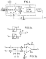
- the circuit 3 for calculating the average value in fact constitutes a low-pass filter type circuit ensuring the functions of integration and algebraic summation of the signals of first and second pulse S imp, S p delivered by the first, respectively the second channel 1.2.
- the subtractor circuit 33 can comprise, as shown in FIG. 5a, a first and a second integrator circuit 31, 32 receiving respectively the first and the second pulse S1, S p and delivering a corresponding integrated signal, and a subtractor circuit 33 receiving on its positive and negative inputs the integrated signal delivered by the first respectively the second integrator circuit 31,32.
- the subtractor circuit 33 delivers the phase comparison signal V0.
- this type of circuit can be produced, as shown in FIG. 5b, from an operational amplifier 300 mounted as a differential amplifier and looped back in feedback through a series circuit R1C1 on the negative input of the latter.
- phase comparator device object of the present invention, is particularly suitable for operation on the basis of data constituted by a digital signal of NRZ type for " no return to zero " in English language. Saxon.
- phase comparator device according to the invention due because it is adapted to detect transitions, can be used with all types of digital signal coding formats, such as RZ or CMI type codings for example.
Abstract
Description
Dans les techniques relatives à la transmission ou au traitement de signaux numériques, il est indispensable d'assurer une transmission ou un traitement à haut débit en parfait synchronisme avec un signal d'horloge de référence.In techniques relating to the transmission or processing of digital signals, it is essential to ensure high speed transmission or processing in perfect synchronism with a reference clock signal.
A cet effet, les circuits permettant ce type d'opérations nécessitent la mise en oeuvre de circuits récupérateurs de rythme.To this end, the circuits allowing this type of operation require the implementation of rhythm recovery circuits.
L'amélioration des performances de ces derniers circuits consiste, selon les techniques actuelles, soit à réduire les effets des différentes sources de bruit, notamment de bruit de phase, présentes dans ces circuits, afin d'en améliorer les performances relativement au phénomène de "gigue" connu sous la dénomination de "jitter" en vocable anglo-saxon, soit à minimiser les erreurs de transmission en améliorant la tolérance au bruit du circuit récupérateur de rythme. Cette dernière opération est effectuée lors de la resynchronisation des données numériques, constituées par une suite d'éléments binaires, au moyen d'une bascule bistable synchronisée sur le signal d'horloge de référence et en maintenant le front actif du signal d'horloge en milieu de chaque élément binaire. Une telle mesure implique la synchronisation parfaite du front actif du signal d'horloge et de la demi-période du flux d'éléments binaires.The improvement of the performances of these latter circuits consists, according to current techniques, either of reducing the effects of the different noise sources, in particular of phase noise, present in these circuits, in order to improve the performances relative to the phenomenon of " jitter "known under the name of" jitter "in Anglo-Saxon terms, that is to minimize transmission errors by improving the noise tolerance of the timing recovery circuit. This last operation is carried out during the resynchronization of the digital data, constituted by a series of binary elements, by means of a flip-flop synchronized with the reference clock signal and by maintaining the active edge of the clock signal in middle of each bit. Such a measurement implies perfect synchronization of the active edge of the clock signal and the half-period of the bit stream.
Des circuits récupérateurs de rythme de ce type ont été notamment décrits dans l'article intitulé "A self correcting Clock Recovery Circuit" publié par Charles R. HOGGE, dans la revue technique JOURNAL OF LIGHTWAVE TECHNOLOGY, Vol. LT-3, No.6 Décembre 1985.
Le circuit décrit par l'article précité fournit un excellent résultat car il remplit simultanément les fonctions de régénération et de resynchronisation des données numériques ainsi qu'une auto-correction du maintien en milieu de bit du front actif de l'horloge locale de référence.Rhythm recovery circuits of this type have been described in particular in the article entitled " A self correcting Clock Recovery Circuit " published by Charles R. HOGGE, in the technical journal JOURNAL OF LIGHTWAVE TECHNOLOGY, Vol. LT-3, No. 6 December 1985.
The circuit described by the aforementioned article provides an excellent result because it simultaneously fulfills the functions of regeneration and resynchronization of digital data as well as an auto-correction of the maintenance in the middle of the active front edge of the local reference clock.
Toutefois, une analyse des signaux de sortie 6 et 7 en entrée du comparateur de sortie, ainsi que représenté en figure 1 relative à l'art antérieur correspondant, montre que ces derniers sont, à l'équilibre de phase, décalés de 180°. En conséquence, le signal à intégrer [6-7], délivré par le comparateur de sortie précité, possède une forte ondulation crête à crête, d'amplitude 2A, lorsque l'équilibre de phase est acquis.However, an analysis of
Le signal à intégrer précité, ou signal différentiel, possède donc une amplitude crête à crête importante et une fréquence maximale égale à la fréquence élément binaire ou fréquence bit. Un tel signal est susceptible de constituer une source de "gigue" très importante dans le circuit, sauf à prévoir un traitement de filtrage très soigné. Le phénomène de "gigue" précité peut donc se révéler très gênant, notamment dans les dispositifs de transmission constitués par des éléments successifs en cascade, pour lesquels il est bien connu que le phénomène de "gigue" s'accumule et augmente systématiquement le long de la chaîne de transmission.The aforementioned signal to be integrated, or differential signal, therefore has a significant peak-to-peak amplitude and a maximum frequency equal to the binary element frequency or bit frequency. Such a signal is likely to constitute a very significant source of " jitter " in the circuit, unless a very careful filtering treatment is provided. The above-mentioned " jitter " phenomenon can therefore prove to be very annoying, in particular in transmission devices constituted by successive elements in cascade, for which it is well known that the " jitter " phenomenon accumulates and systematically increases along the chain of transmission.
La présente invention a pour objet la mise en oeuvre d'un dispositif comparateur de phase conservant les avantages obtenus par le circuit décrit dans l'article précité tout en éliminant ou réduisant sensiblement la contribution de celui-ci au phénomène de "gigue".The present invention relates to the implementation of a phase comparator device retaining the advantages obtained by the circuit described in the aforementioned article while eliminating or substantially reducing its contribution to the phenomenon of " jitter ".
Le dispositif comparateur de phase entre transitions d'un signal numérique formé par une suite de bits {ak} et un signal d'horloge Ck à la fréquence élément binaire de ce signal numérique, objet de la présente invention, est remarquable en ce qu'il comprend une première voie de détection permettant, à partir du signal d'horloge Ck et du signal numérique, d'engendrer un signal numérique retardé d'une valeur de retard τ, 0 < τ < T, où T désigne la période du signal numérique, cette première voie de détection comportant en outre un circuit générateur à chaque transition d'une première impulsion dont la durée est variable, proportionnelle au déphasage entre le signal numérique retardé et le signal d'horloge. Une deuxième voie de détection est prévue, laquelle permet, à partir du signal d'horloge et du signal numérique, d'engendrer à chaque transition du signal numérique une deuxième impulsion de durée constante égale à la demi-période du signal d'horloge. Un circuit de calcul de la valeur moyenne, sur au moins un cycle du signal d'horloge, de la différence algébrique entre la première et la deuxième impulsion délivre un signal de comparaison de phase entre signal numérique et signal d'horloge de valeur nulle pour un déphasage nul et un centrage exact de l'impulsion formée par deux transitions consécutives du signal numérique retardé sur un front montant ou descendant du signal d'horloge et de valeur positive ou négative pour un déphasage d'avance respectivement de retard du signal d'horloge par rapport au signal numérique retardé.The device for comparing the phase between transitions of a digital signal formed by a series of bits {ak} and a clock signal Ck at the frequency binary element of this digital signal, object of the present invention, is remarkable in that it comprises a first detection channel making it possible, from the clock signal Ck and the digital signal, to generate a digital signal delayed by a delay value τ, 0 <τ <T, where T denotes the period of the signal digital, this first detection channel further comprising a generator circuit at each transition of a first pulse whose duration is variable, proportional to the phase shift between the digital signal delayed and the clock signal. A second detection channel is provided, which makes it possible, from the clock signal and the digital signal, to generate at each transition of the digital signal a second pulse of constant duration equal to the half-period of the clock signal. A circuit for calculating the average value, over at least one cycle of the clock signal, of the algebraic difference between the first and the second pulse delivers a phase comparison signal between digital signal and clock signal of zero value for zero phase shift and exact centering of the pulse formed by two consecutive transitions of the digital signal delayed on a rising or falling edge of the clock signal and of positive or negative value for a phase shift of the signal signal delay respectively clock versus delayed digital signal.
Le dispositif comparateur de phase, objet de la présente invention, trouve application à la réalisation de circuits électroniques de traitement de signaux numériques, notamment sous forme de circuits intégrés.The phase comparator device, object of the present invention, finds application in the production of electronic circuits for processing digital signals, in particular in the form of integrated circuits.
Il sera mieux compris dans ses éléments structurels et/ou fonctionnels à la lecture de la description et à l'observation des dessins ci-après dans lesquels, outre la figure 1 relative à l'art antérieur,
- la figure 2a représente le schéma d'un dispositif comparateur de phase, objet de la présente invention,
- les figures 2b, 2c et 2d représentent des chronogrammes des signaux mis en oeuvre par le dispositif représenté en figure 2a dans le cas d'une avance, d'un retard respectivement d'une égalité de phase d'un signal d'horloge par rapport à un signal numérique de données, retardé par rapport à un signal numérique de données d'origine,
- la figure 3a représente une variante de réalisation du dispositif comparateur de phase représenté en figure 2a, en vue d'une application à haute fréquence ou haut débit de données,
- la figure 3b représente un chronogramme des signaux mis en oeuvre par le dispositif de la figure 3a,
- la figure 4 représente une application particulière avantageuse du comparateur de phase représenté en figure 2a ou 3a à la réalisation d'une boucle à verrouillage de phase permettant, à partir d'un signal numérique d'entrée, de restaurer un signal d'horloge local parfaitement synchrone du signal numérique d'entrée,
- les figures 5a et 5b sont relatives à un mode de réalisation avantageux d'un circuit générateur du signal de comparaison de phase.
- FIG. 2a represents the diagram of a phase comparator device, object of the present invention,
- FIGS. 2b, 2c and 2d represent timing diagrams of the signals implemented by the device represented in FIG. 2a in the case of an advance, of a delay respectively of a phase equality of a clock signal with respect to to a digital data signal, delayed with respect to an original digital data signal,
- FIG. 3a represents an alternative embodiment of the phase comparator device shown in FIG. 2a, for a high frequency or high data rate application,
- FIG. 3b represents a timing diagram of the signals used by the device of FIG. 3a,
- FIG. 4 represents a particular advantageous application of the phase comparator represented in FIG. 2a or 3a to the production of a phase locked loop making it possible, from a digital input signal, to restore a local clock signal perfectly synchronized with the digital input signal,
- FIGS. 5a and 5b relate to an advantageous embodiment of a circuit generating the phase comparison signal.
Une description plus détaillée d'un dispositif comparateur de phase entre transitions d'un signal numérique, objet de la présente invention, sera maintenant donnée en liaison avec la figure 2a.A more detailed description of a phase comparator device between transitions of a digital signal, object of the present invention, will now be given in connection with FIG. 2a.
D'une manière générale, on indique que le signal numérique est un signal de données, référencé par la lettre D, formé par une suite de bits ou éléments binaires, notée { ak} . Bien entendu, on dispose pour la mise en oeuvre du dispositif comparateur de phase, objet de la présente invention, d'un signal d'horloge, noté Ck, ce signal d'horloge étant un signal à la fréquence bit ou fréquence élément binaire du signal numérique précité, réputé présenter une période correspondant à la durée de chaque bit, désignée par T. A priori, et en raison des vicissitudes de mise en oeuvre des circuits électroniques, le signal numérique d'entrée, ou signal numérique d'origine D, et le signal d'horloge Ck peuvent présenter un phénomène de "gigue" de phase néfaste au traitement et à la transmission correcte des données véhiculées par le signal numérique d'entrée précité.In general, it is indicated that the digital signal is a data signal, referenced by the letter D, formed by a series of bits or binary elements, denoted {ak}. Of course, for the implementation of the phase comparator device, object of the present invention, there is a clock signal, denoted Ck, this clock signal being a signal at the bit frequency or binary element frequency of the aforementioned digital signal, deemed to have a period corresponding to the duration of each bit, designated by T. A priori, and due to the vicissitudes of implementation of the electronic circuits, the digital input signal, or original digital signal D , and the clock signal Ck can exhibit a phase " jitter " phenomenon detrimental to the processing and correct transmission of the data conveyed by the aforementioned digital input signal.
Ainsi qu'on l'a représenté en figure 2a, on indique que le dispositif comparateur de phase, objet de la présente invention, comprend une première voie de détection, notée 1, permettant, à partir du signal d'horloge Ck et du signal numérique D, d'engendrer un signal numérique retardé, noté DR, d'une valeur de retard τ comprise entre 0 < τ < T. Le signal numérique retardé DR peut être engendré par l'intermédiaire d'un circuit de retard 10, lequel sera décrit plus en détail ultérieurement dans la description.As shown in FIG. 2a, it is indicated that the phase comparator device, object of the present invention, comprises a first detection channel, denoted 1, allowing, from the clock signal Ck and the signal digital D, to generate a delayed digital signal, noted DR, with a delay value τ between 0 <τ <T. The delayed digital signal DR can be generated via a
La première voie 1 comporte en outre un circuit 11 générateur à chaque transition du signal numérique D d'une première impulsion dont la durée est variable, proportionnelle au déphasage entre le signal numérique retardé DR et le signal d'horloge Ck. Ce signal est noté S₁ sur la figure 2a, la sortie du circuit générateur 11 constituant en fait la sortie de la première voie de détection 1 précédemment mentionnée.The
Le dispositif comparateur, selon l'invention, comporte en outre une deuxième voie de détection, notée 2, permettant, à partir du signal d'horloge Ck et du signal numérique D, d'engendrer à chaque transition du signal numérique précité, une deuxième impulsion calibrée de durée constante, égale à la demi-période du signal d'horloge Ck. La deuxième impulsion calibrée est notée Sp sur la figure 2a.The comparator device according to the invention further comprises a second detection channel, denoted 2, making it possible, from the clock signal Ck and the digital signal D, to generate at each transition of the above-mentioned digital signal, a second calibrated pulse of constant duration, equal to the half-period of the clock signal Ck. The second calibrated pulse is denoted Sp in FIG. 2a.
Enfin, un circuit de calcul 3 de la valeur moyenne de la différence entre la première et la deuxième impulsion est prévu, ce circuit de calcul 3 délivrant un signal de comparaison de phase V₀ entre signal numérique retardé DR et signal d'horloge de valeur nulle pour un déphasage nul et un centrage exact de l'impulsion formée par deux transitions consécutives du signal numérique retardé DR sur un front montant ou descendant du signal d'horloge. Le signal de comparaison de phase V₀ a, au contraire, une valeur moyenne positive, respectivement négative, pour un déphasage d'avance respectivement de retard du signal d'horloge Ck par rapport au signal numérique retardé DR précité.Finally, a
Ainsi qu'on l'a en outre représenté en figure 2a, on indique que la première voie de détection 1 comprend, connectés en cascade, le circuit de retard 10 permettant d'introduire la valeur de retard τ dans les conditions précitées sur le signal numérique d'entrée D pour engendrer le signal numérique retardé DR, et le circuit 11 générateur de la première impulsion S₁. D'une manière générale, on indique que le circuit de retard 10 peut être réalisé soit par un circuit dit externe, c'est-à-dire par un circuit de type ligne à retard analogique, soit, au contraire, par un circuit interne lorsque le circuit de retard 10 est réalisé par exemple par l'intermédiaire de portes logiques successives, entraînant chacune un retard élémentaire de valeur déterminée. Dans ce deuxième mode de réalisation, le circuit de retard 10 est dit interne en raison du fait que les portes logiques constitutives de ce dernier peuvent être intégrées sur un même substrat pour réaliser le dispositif comparateur de phase, objet de la présente invention, tel que représenté en figure 2a.As has also been shown in FIG. 2a, it is indicated that the
En outre, la première voie de détection 1 comprend le circuit 11 générateur de la première impulsion S1, ce circuit comprenant par exemple un premier circuit logique 111 de type OU exclusif, recevant sur une première entrée le signal numérique retardé DR, et une bascule bistable synchronisée, notée 110, cette bascule étant synchronisée sur le signal d'horloge Ck. Ainsi, la bascule bistable synchronisée 110 reçoit sur son entrée d'horloge le signal d'horloge Ck, sur son entrée D le signal numérique retardé DR, et délivre à sa sortie Q un signal numérique retardé synchronisé, noté D₁, lequel est directement délivré à la deuxième entrée du premier circuit logique de type OU exclusif 111. Ce dernier délivre la première impulsion S₁ en sortie de la première voie de détection 1.In addition, the
Ainsi qu'on l'a également représenté sur la figure 2a, la deuxième voie de détection 2 comprend, connectés en cascade, un circuit générateur 20 d'un signal numérique décalé d'une demi-période par rapport au signal numérique retardé synchronisé à partir du signal numérique d'entrée D. En sortie du circuit générateur 20, est connecté un circuit générateur, à partir du signal numérique retardé d'une demi-période délivré par le circuit générateur 20, de la deuxième impulsion Sp, ce circuit générateur de la deuxième impulsion portant la référence 21 comprenant, de manière semblable au circuit 11 de la première voie, un deuxième circuit logique de type OU exclusif, noté 211, recevant sur une première entrée le signal numérique décalé d'une demi-période, signal noté D₂, et une bascule bistable synchronisée, notée 210, cette bascule étant synchronisée sur le signal d'horloge Ck. La bascule bistable 210 reçoit sur son entrée D le signal logique décalé d'une demi-période, noté D₂, et sur son entrée d'horloge, le signal Ck précité. La sortie Q de la deuxième bascule bistable synchronisée 210 délivre un signal D₃ à une deuxième entrée de la deuxième porte OU exclusif 211.As also shown in FIG. 2a, the
En outre, on indique que le circuit générateur 20 du signal numérique décalé d'une demi-période D₂ par rapport au signal numérique retardé synchronisé peut être formé par une bascule bistable synchronisée sur le signal d'horloge complémenté ![]()
![]()
![]()
![]()
Le fonctionnement du dispositif, objet de la présente invention, tel que représenté en figure 2a, sera explicité en liaison avec les figures 2b, 2c et 2d ci-après.The operation of the device, object of the present invention, as shown in Figure 2a, will be explained in connection with Figures 2b, 2c and 2d below.
- Figure 2b : horloge en avance de phase.
Dans le cas de la figure 2b précitée, on indique que le chronogramme représenté correspond au cas où l'horloge Ck est en avance de phase par rapport au centre des deux transitions successives, représentatives par exemple de la transmission d'éléments binaires de valeurs successives 0, 1, 0. Dans ce cas, le front montant du signal d'horloge, considéré comme le front actif, présente une avance de phase Δφ < O par rapport au centre de l'impulsion formée par les deux transitions précitées. Le signal D₂, délivré par la bascule bistable synchronisée 20 sur le signal d'horloge complémenté ![]()
![]()
In the case of FIG. 2b above, it is indicated that the chronogram represented corresponds to the case where the clock Ck is in phase advance with respect to the center of the two successive transitions, representative for example of the transmission of binary elements of ![]()
![]()
La valeur moyenne de la deuxième impulsion Sp est supérieure à la valeur moyenne de la première impulsion S₁ en raison du déphasage Δφ négatif, représenté entre le signal numérique retardé DR et le signal d'horloge Ck. La première impulsion S₁ délivrée par le premier circuit OU exclusif 111, a pour valeur, pour chacune des transitions du signal numérique d'entrée D et donc du signal numérique retardé DR, le décalage entre les fronts montants du signal numérique retardé DR et du signal D₁, respectivement entre les fronts descendants de ces deux mêmes signaux, ainsi que représenté sur la figure 2b. Dans ces conditions, la valeur moyenne de la différence S₁ - Sp, différence algébrique de la première et de la deuxième impulsion, la deuxième impulsion ayant toujours pour valeur la demi-période T/2, est donc négative.The average value of the second pulse S p is greater than the average value of the first pulse S₁ due to the negative phase shift Δφ, represented between the delayed digital signal DR and the clock signal Ck. The first pulse S₁ delivered by the first exclusive OR circuit 111, has the value, for each of the transitions of the digital input signal D and therefore of the delayed digital signal DR, the offset between the rising edges of the delayed digital signal DR and of the signal D₁, respectively between the falling edges of these two same signals, as shown in Figure 2b. Under these conditions, the average value of the difference S₁ - S p , algebraic difference of the first and the second pulse, the second pulse always having for value the half-period T / 2, is therefore negative.
- Figure 2c : horloge en retard de phase.
Dans le cas où, au contraire, le signal d'horloge, c'est-à-dire le front montant de celui-ci, est en retard par rapport au centre de l'impulsion formé par les deux transitions successives précitées Δφ > 0, représenté sur la figure 2c précité, le signal D₂ délivré par la bascule bistable synchronisée 20 est en avance d'une demi-période T/2 par rapport au signal D₁ délivré par la bascule bistable 110. En d'autres termes, le signal D₁ délivré par la bascule synchronisée précitée 110 est en retard de plus d'une demi-période par rapport au signal numérique retardé DR, Δφ > 0, et le signal S₁ résultat du OU exclusif entre ces deux signaux présente donc une durée à l'état haut supérieure à la demi-période T/2. Dans ce cas, la valeur moyenne de la deuxième impulsion Sp dont la durée est fixe, calibrée et égale à T/2, est inférieure à celle de la première impulsion S₁, ce qui indique que le signal d'horloge Ck est en retard par rapport au signal numérique retardé DR. La valeur moyenne de la différence entre la première et la deuxième impulsion S₁-Sp est cette fois positive.- Figure 2c: late phase clock.
In the case where, on the contrary, the clock signal, that is to say the rising edge thereof, is late with respect to the center of the pulse formed by the two above-mentioned successive transitions Δφ> 0 , shown in FIG. 2c above, the signal D₂ delivered by the synchronized flip-
Figure 2d : horloge et données retardées DR en phase.
Dans le cas de la figure 2d précitée, le signal d'horloge Ck et le signal numérique retardé DR sont en phase, le front montant du signal d'horloge étant exactement centré sur la demi-durée entre deux transitions. Le décalage de phase est alors nul, Δφ = 0. Dans ce cas, et en référence au fonctionnement précédemment décrit dans le cas de l'avance ou du retard de phase, on comprend bien sûr que, par symétrie, la première impulsion S₁ a une durée égale à la demi-période T/2, cette durée étant donc égale à celle de la deuxième impulsion Sp. Les première et deuxième impulsions S₁ et Sp ont exactement la même durée, et donc même valeur moyenne, et la valeur moyenne de la différence entre première et deuxième impulsion S₁ - Sp est donc nulle. On constate en outre, contrairement aux comparateurs de phase de l'art antérieur tels que décrits dans l'article précédemment mentionné dans la description, que les signaux S₁ et Sp sont exactement en phase. La différence obtenue pour le signal différentiel S₁ - Sp est donc de valeur nulle, c'est-à-dire sans aucune ondulation à l'équilibre. Le dispositif objet de la présente invention permet donc d'améliorer notoirement les performances vis-à-vis du phénomène de "gigue", la contribution à ce phénomène étant ainsi sensiblement supprimée.Figure 2d: DR clock and delayed data in phase.
In the case of FIG. 2d above, the clock signal Ck and the delayed digital signal DR are in phase, the rising edge of the clock signal being exactly centered on the half-duration between two transitions. The phase shift is then zero, Δφ = 0. In this case, and with reference to the operation previously described in the case of phase advance or delay, it is of course understood that, by symmetry, the first pulse S₁ a a duration equal to the half-period T / 2, this duration therefore being equal to that of the second pulse S p . The first and second pulses S₁ and S p have exactly the same duration, and therefore the same average value, and the average value of the difference between first and second pulse S₁ - S p is therefore zero. It is further noted, unlike the phase comparators of the prior art as described in the article previously mentioned in the description, that the signals S₁ and S p are exactly in phase. The difference obtained for the differential signal S₁ - S p is therefore of zero value, that is to say without any ripple at equilibrium. The device that is the subject of the present invention therefore makes it possible to improve performance vis-à-vis the phenomenon of " jitter ", the contribution to this phenomenon thus being substantially eliminated.
D'une manière générale, on indique que la valeur du retard t apporté par le circuit 10 de la première voie de détection peut être choisie de manière arbitraire quelconque, pourvu que cette valeur soit différente de 0 ou T. La bascule bistable synchronisée 20, synchronisée sur le signal d'horloge complémenté ![]()
![]()
Pour cette raison, lorsque le système est en équilibre en l'absence de déphasage, selon le chronogramme de la figure 2d, pour une valeur de retard τ = 0, le front descendant du signal d'horloge Ck est aligné avec les transitions du signal numérique d'entrée. Une telle situation est susceptible d'entraîner des conflits lors de la resynchronisation par l'intermédiaire de la bascule bistable synchronisée 20. Pour assurer l'absence d'une telle situation, il suffit de prendre une valeur de retard τ supérieure au temps d'établissement de la bascule bistable synchronisée 20.For this reason, when the system is in equilibrium in the absence of phase shift, according to the timing diagram of FIG. 2d, for a delay value τ = 0, the falling edge of the clock signal Ck is aligned with the transitions of the signal digital input. Such a situation is likely to cause conflicts during resynchronization by means of the synchronized flip-
Si, au contraire, la valeur de retard τ = T, on retrouve un phénomène semblable. Il est alors souhaitable d'assurer une valeur de retard τ inférieure à la durée de la période T diminuée du temps de maintien de la bascule bistable synchronisée 20. D'où la valeur précédemment mentionnée pour la valeur de retard τ précitée.If, on the contrary, the delay value τ = T, we find a similar phenomenon. It is then desirable to ensure a delay value τ less than the duration of the period T minus the holding time of the synchronized flip-
Une valeur optimale du retard τ est donnée par t = T/2. Cette valeur optimale permet d'introduire la marge de phase statique optimale, toute autre valeur τ ≠ T/2 ε ] 0,T [ ne présentant pas cette caractéristique. Contrairement au comparateur de Hogge où la marge de phase est constante, la marge de phase statique n'est pas conservée sur toute la plage de durée possible de retard.An optimal value of the delay τ is given by t = T / 2. This optimal value makes it possible to introduce the optimal static phase margin, any other value τ ≠ T / 2 ε] 0, T [not having this characteristic. Unlike the Hogge comparator where the phase margin is constant, the static phase margin is not retained over the entire range of possible delay time.
Dans un mode de réalisation pratique, on indique que les bascules bistables synchronisées portant la référence 110, 20 et 210, peuvent être réalisées de manière classique ou bien être constituées par deux bascules verrouillées, "latches" en langage anglo-saxon, et montées en cascade de type maître-esclave. Les sorties Q, ![]()
![]()
Les circuits de type OU exclusif 111 et 211 peuvent être réalisés par des circuits de type classique.The circuits of the exclusive OR
En première conclusion, on indique que le dispositif comparateur de phase, objet de la présente invention, permet de délivrer un signal de comparaison de phase, en l'absence de déphasage, issu d'une tension différentielle d'erreur présentant une ondulation crête nulle, ce qui bien entendu permet de diminuer sensiblement la contribution d'un tel circuit au phénomène de "gigue". En outre, on constate à l'observation des chronogrammes représentés en figures 2b, 2c et 2d, que le dispositif selon l'invention permet d'effectuer un centrage automatique des fronts montants du signal d'horloge Ck en milieu de bit, c'est-à-dire bien sûr en milieu des transitions correspondantes du signal numérique retardé DR en assurant ainsi une resynchronisation du signal de données retardé idéal sur le signal d'horloge précité. On indique en outre, en raison de la structure particulière du dispositif, objet de la présente invention, tel que représentée en figure 2a, que les signaux numériques engendrés par les sorties Q ou ![]()
![]()
Une description plus détaillée d'un dispositif comparateur de phase, conforme à l'objet de la présente invention, appliqué plus particulièrement à la transmission de signal numérique à haute fréquence ou à haut débit sera maintenant donnée en liaison avec la figure 3a.A more detailed description of a phase comparator device, in accordance with the object of the present invention, applied more particularly to the transmission of digital signal at high frequency or at high speed will now be given in connection with FIG. 3a.
Sur la figure précitée, on indique que les mêmes références représentent les mêmes éléments que dans le cas de la figure 2a précédente. Toutefois, la première entrée du premier circuit logique de type OU exclusif 111 de la première voie de détection 1 comprend un circuit de retard 112 permettant d'introduire une compensation, sur le signal numérique retardé DR, du temps de propagation et de transition introduit par la première bascule bistable synchronisée 110. Le circuit de retard 111 délivre en fait, sur l'entrée du premier circuit de type OU exclusif 111, un signal numérique retardé compensé, noté DR*.In the above-mentioned figure, it is indicated that the same references represent the same elements as in the case of the preceding figure 2a. However, the first input of the first exclusive OR type logic circuit 111 of the
D'une manière générale, on indique que, afin de compenser exactement les temps de propagation des différents signaux dans les différents circuits permettant la mise en oeuvre de la première et de la deuxième voie de détection 1,2, il est opportun que les différents éléments soient parfaitement appairés afin que ceux-ci présentent les mêmes temps de propagation pour de larges plages de conditions de fonctionnement en température, tension d'alimentation, par exemple. C'est le cas en particulier pour les circuits logiques de type OU exclusif 111 et 211.In general, it is indicated that, in order to exactly compensate the propagation times of the different signals in the different circuits allowing the implementation of the first and the
En outre, on indique que le retard τ₁ introduit par le circuit de retard 112 doit présenter les mêmes variations que le temps de propagation ou d'établissement de la bascule bistable synchronisée 110 pour engendrer le signal D₁, dans des conditions de fonctionnement semblables.In addition, it is indicated that the delay τ₁ introduced by the
A l'équilibre, c'est-à-dire en l'absence de déphasage entre le signal d'horloge Ck et le signal numérique retardé DR, un chronogramme des signaux correspondants est représenté en figure 3b.At equilibrium, that is to say in the absence of phase shift between the clock signal Ck and the delayed digital signal DR, a timing diagram of the corresponding signals is shown in FIG. 3b.
Sur la figure 3b précitée, on indique que les deux circuits de type OU exclusif 111 et 211 ont même temps de propagation = Tp(XOR), les trois bascules bistables synchronisées 110, 20, 210 ont même temps de propagation = TpD,![]()
- la valeur du retard τ introduit par le circuit de retard 10 est quelconque et fixée dans les conditions précédemment données dans la description.In the aforementioned FIG. 3b, it is indicated that the two exclusive OR ![]()
- The value of the delay τ introduced by the
Une application particulièrement avantageuse du dispositif comparateur de phase, objet de la présente invention, sera maintenant décrite en liaison avec la figure 4.A particularly advantageous application of the phase comparator device, object of the present invention, will now be described in conjunction with FIG. 4.
Parmi toutes les applications envisageables du dispositif selon l'invention, une application très importante concerne l'utilisation de ce dernier dans une boucle de verrouillage de phase, une telle boucle étant constituée afin d'extraire un signal d'horloge local à partir d'un signal numérique d'entrée de données, dit signal de données d'origine.Among all the possible applications of the device according to the invention, a very important application concerns the use of the latter in a loop phase lock, such a loop being formed in order to extract a local clock signal from a digital data input signal, called the original data signal.
De manière classique, ainsi que représenté sur la figure 4, la boucle à verrouillage de phase peut comprendre un dispositif comparateur de phase, tel que décrit précédemment dans la description, portant la référence C, comprenant un circuit comparateur de phase proprement dit formé par la première et la deuxième voie de détection 1,2 et par un circuit de calcul de la valeur moyenne portant la référence 3. Le comparateur C peut alors être suivi d'un circuit de type oscillateur local contrôlé en tension, noté VCO, lequel reçoit sur son entrée de commande en tension le signal de détection de phase V₀, le circuit oscillateur local commandé en tension délivrant le signal d'horloge Ck. Ce signal d'horloge peut alors bien entendu être utilisé comme signal d'horloge local. La sortie du circuit oscillateur local commandé en tension VCO est alors rebouclée sur les entrées de signal d'horloge Ck et de signal d'horloge ![]()
![]()
Le signal D sortie est le signal numérique d'entrée resynchronisé sur le signal d'horloge Ck et peut être pris sur l'une des sorties précitées des trois bascules bistables synchronisées 110, 20, 210.The output signal D is the digital input signal resynchronized on the clock signal Ck and can be taken from one of the aforementioned outputs of the three synchronized flip-
Dans le cas d'une application haute fréquence ou haut débit, le circuit de retard 112 pourra avantageusement être réalisé à l'aide de deux bascules verrouillées "latches", montées en mode transparent. On assure ainsi que le retard τ₁ est idéalement appairé avec le temps de propagation des trois bascules bistables synchronisées précitées lorsque celles-ci sont formées de manière identique par deux bascules verrouillées.In the case of a high frequency or high speed application, the
En ce qui concerne le circuit 3, on indique que celui-ci peut délivrer un signal correspondant, soit à une tension, soit à un courant, lequel permet de commander l'oscillateur VCO.With regard to
L'oscillateur précité est choisi de façon à présenter une fréquence centrale très stable et peut donc être constitué par un oscillateur à cristal par exemple.The aforementioned oscillator is chosen so as to have a very stable central frequency and can therefore be constituted by a crystal oscillator for example.
Le circuit 3 de calcul de la valeur moyenne constitue en fait un circuit de type filtre passe-bas assurant les fonctions d'intégration et de sommation algébrique des signaux de première et deuxième impulsion S₁, Sp délivrés par la première, respectivement la deuxième voie de détection 1,2.The
A ce titre, il peut comporter, ainsi que représenté en figure 5a, un premier et un deuxième circuit intégrateur 31, 32 recevant respectivement la première et la deuxième impulsion S₁, Sp et délivrant un signal correspondant intégré, et un circuit soustracteur 33 recevant sur ses entrées positive respectivement négative le signal intégré délivré par le premier respectivement le deuxième circuit intégrateur 31,32. Le circuit soustracteur 33 délivre le signal de comparaison de phase V₀.As such, it can comprise, as shown in FIG. 5a, a first and a
En ce qui concerne la réalisation pratique du circuit 3 et afin de réaliser les fonctions représentées en figure 5a, ce type de circuit pourra être réalisé, ainsi que représenté en figure 5b, à partir d'un amplificateur opérationnel 300 monté en amplificateur différentiel et rebouclé en contre-réaction par l'intermédiaire d'un circuit série R₁C₁ sur l'entrée négative de ce dernier.With regard to the practical implementation of
D'une manière générale, on indique que le dispositif comparateur de phase, objet de la présente invention, est particulièrement adapté à un fonctionnement à partir de données constituées par un signal numérique de type NRZ pour "non return to zero" en langage anglo-saxon. Toutefois, le dispositif comparateur de phase selon l'invention, en raison du fait que celui-ci est adapté à détecter des transitions, peut être utilisé avec tous types de formats de codage de signaux numériques, tels que codages de type RZ ou CMI par exemple.In general, it is indicated that the phase comparator device, object of the present invention, is particularly suitable for operation on the basis of data constituted by a digital signal of NRZ type for " no return to zero " in English language. Saxon. However, the phase comparator device according to the invention, due because it is adapted to detect transitions, can be used with all types of digital signal coding formats, such as RZ or CMI type codings for example.
Claims (7)
Applications Claiming Priority (2)
| Application Number | Priority Date | Filing Date | Title |
|---|---|---|---|
| FR9407662 | 1994-06-22 | ||
| FR9407662A FR2721780B1 (en) | 1994-06-22 | 1994-06-22 | Phase comparator device. |
Publications (2)
| Publication Number | Publication Date |
|---|---|
| EP0689315A1 true EP0689315A1 (en) | 1995-12-27 |
| EP0689315B1 EP0689315B1 (en) | 2000-03-22 |
Family
ID=9464519
Family Applications (1)
| Application Number | Title | Priority Date | Filing Date |
|---|---|---|---|
| EP19950401435 Expired - Lifetime EP0689315B1 (en) | 1994-06-22 | 1995-06-19 | Phase comparator |
Country Status (3)
| Country | Link |
|---|---|
| EP (1) | EP0689315B1 (en) |
| DE (1) | DE69515735T2 (en) |
| FR (1) | FR2721780B1 (en) |
Cited By (5)
| Publication number | Priority date | Publication date | Assignee | Title |
|---|---|---|---|---|
| EP0874449A2 (en) * | 1997-04-24 | 1998-10-28 | Nortel Networks Corporation | A method and apparatus for phase detection in digital signals |
| US6028898A (en) * | 1997-04-24 | 2000-02-22 | Nortel Networks Corporation | Signal regenerator |
| EP1677422A1 (en) * | 2004-12-30 | 2006-07-05 | Alcatel | Apparatus for conversion of a transmitted signal into a binary signal |
| WO2008095508A1 (en) * | 2007-02-05 | 2008-08-14 | Tes Electronic Solutions Gmbh | Pulse generator |
| ITTO20130347A1 (en) * | 2013-04-29 | 2014-10-30 | St Microelectronics Srl | CIRCUIT AND CALIBRATION METHOD FOR A DIGITALLY CONTROLLED OSCILLATOR |
Citations (3)
| Publication number | Priority date | Publication date | Assignee | Title |
|---|---|---|---|---|
| US4535459A (en) * | 1983-05-26 | 1985-08-13 | Rockwell International Corporation | Signal detection apparatus |
| EP0286329A2 (en) * | 1987-04-07 | 1988-10-12 | Gigabit Logic Inc | Phase locked loop clock synchroniser and signal detector |
| EP0500473A1 (en) * | 1991-02-22 | 1992-08-26 | SAT (Société Anonyme de Télécommunications) | Phase/frequency comparator for a clock recovery circuit |
-
1994
- 1994-06-22 FR FR9407662A patent/FR2721780B1/en not_active Expired - Fee Related
-
1995
- 1995-06-19 EP EP19950401435 patent/EP0689315B1/en not_active Expired - Lifetime
- 1995-06-19 DE DE1995615735 patent/DE69515735T2/en not_active Expired - Lifetime
Patent Citations (3)
| Publication number | Priority date | Publication date | Assignee | Title |
|---|---|---|---|---|
| US4535459A (en) * | 1983-05-26 | 1985-08-13 | Rockwell International Corporation | Signal detection apparatus |
| EP0286329A2 (en) * | 1987-04-07 | 1988-10-12 | Gigabit Logic Inc | Phase locked loop clock synchroniser and signal detector |
| EP0500473A1 (en) * | 1991-02-22 | 1992-08-26 | SAT (Société Anonyme de Télécommunications) | Phase/frequency comparator for a clock recovery circuit |
Non-Patent Citations (2)
| Title |
|---|
| C.H.HOGGE: "A SELF CORRECTING CLOCK RECOVERY CIRCUIT", JOURNAL OF LIGHTWAVE TECHNOLOGY, vol. 3, no. 6, December 1985 (1985-12-01), pages 1312 - 1314 * |
| C.R. HOGGE: "A self correcting Clock Recovery Circuit", JOURNAL OF LIGHTWAVE TECHNOLOGY, vol. LT-3, no. 6, December 1985 (1985-12-01) |
Cited By (8)
| Publication number | Priority date | Publication date | Assignee | Title |
|---|---|---|---|---|
| EP0874449A2 (en) * | 1997-04-24 | 1998-10-28 | Nortel Networks Corporation | A method and apparatus for phase detection in digital signals |
| EP0874449A3 (en) * | 1997-04-24 | 1999-11-10 | Nortel Networks Corporation | A method and apparatus for phase detection in digital signals |
| US6028898A (en) * | 1997-04-24 | 2000-02-22 | Nortel Networks Corporation | Signal regenerator |
| EP1677422A1 (en) * | 2004-12-30 | 2006-07-05 | Alcatel | Apparatus for conversion of a transmitted signal into a binary signal |
| FR2880482A1 (en) * | 2004-12-30 | 2006-07-07 | Cit Alcatel | DEVICE FOR CONVERTING A SIGNAL TRANSMITTED TO A DIGITAL SIGNAL |
| WO2008095508A1 (en) * | 2007-02-05 | 2008-08-14 | Tes Electronic Solutions Gmbh | Pulse generator |
| ITTO20130347A1 (en) * | 2013-04-29 | 2014-10-30 | St Microelectronics Srl | CIRCUIT AND CALIBRATION METHOD FOR A DIGITALLY CONTROLLED OSCILLATOR |
| US9231597B2 (en) | 2013-04-29 | 2016-01-05 | Stmicroelectronics S.R.L. | Digitally controlled oscillator calibration circuit and method |
Also Published As
| Publication number | Publication date |
|---|---|
| DE69515735D1 (en) | 2000-04-27 |
| EP0689315B1 (en) | 2000-03-22 |
| FR2721780A1 (en) | 1995-12-29 |
| FR2721780B1 (en) | 1996-08-30 |
| DE69515735T2 (en) | 2000-11-09 |
Similar Documents
| Publication | Publication Date | Title |
|---|---|---|
| EP0716501B1 (en) | Phase comparator of a digital signal and a clock signal, and corresponding phase locked loop | |
| JPH05276028A (en) | Phase detector for extremely high-frequency clock and data restoring circuit | |
| EP2137873A2 (en) | Clock extraction device with digital phase lock, requiring no external control | |
| FR2880482A1 (en) | DEVICE FOR CONVERTING A SIGNAL TRANSMITTED TO A DIGITAL SIGNAL | |
| EP0142440A2 (en) | Generating device for a frequency being a fraction of a reference frequency | |
| EP0015014A1 (en) | Device for the rapid synchronisation of a clock | |
| FR2509890A1 (en) | DATA READING APPARATUS FOR DATA TRANSMISSION | |
| US20020181360A1 (en) | Clock adjusting device for use with data reproducing apparatus, offset detecting device, and data reporducing apparatus | |
| EP0689315B1 (en) | Phase comparator | |
| FR2736231A1 (en) | DIGITAL COMMUNICATION SYSTEM COMPRISING A RECEIVER HAVING A RHYTHM RECOVERY DEVICE | |
| EP0680170A1 (en) | Circuit for the transmission of a line-coded signal on a telephone line with a frequency synchroniser | |
| EP0026699A1 (en) | Method and device for coding digital data, device for decoding digital data and a transmission system comprising such a device | |
| EP0023852A1 (en) | Method and device for adjusting the phase of a local clock | |
| EP0696116B1 (en) | Method for sampling a serial digital signal | |
| EP1073204B1 (en) | Arrangement for synchronizing a reference event of an analog signal to a clock signal | |
| EP0035295A1 (en) | Clock phase control method for a digital data receiving system, phase recovery circuit for carrying out this method and digital data receiving system comprising this circuit | |
| FR2646742A1 (en) | DEVICE FOR SYNCHRONIZING A PSEUDO-BINARY SIGNAL WITH A REGENERATED CLOCK SIGNAL WITH PHASE HOPES | |
| CA2082288C (en) | Method and device for recovering a clock signal from a received signal | |
| EP0174880B1 (en) | Arrangement for the localisation of the transitions of a data signal in respect of a clock signal, and synchronisation mechanism using such an arrangement | |
| FR2573592A1 (en) | Oscillator circuit phase-locked to a signal of predetermined frequency | |
| EP0905946B1 (en) | Control of the sampling of biphase signals | |
| FR2568738A1 (en) | Device for recovering the clock signal in a digital transmission | |
| FR2755552A1 (en) | Clock signal duplication device for FIFO memory control | |
| EP0237408B1 (en) | Method and device for asynchronous clock recovery for digital transmission systems | |
| JP3618787B2 (en) | Signal processing device |
Legal Events
| Date | Code | Title | Description |
|---|---|---|---|
| PUAI | Public reference made under article 153(3) epc to a published international application that has entered the european phase |
Free format text: ORIGINAL CODE: 0009012 |
|
| 17P | Request for examination filed |
Effective date: 19951027 |
|
| AK | Designated contracting states |
Kind code of ref document: A1 Designated state(s): DE FR GB IT |
|
| RAP1 | Party data changed (applicant data changed or rights of an application transferred) |
Owner name: MHS |
|
| GRAG | Despatch of communication of intention to grant |
Free format text: ORIGINAL CODE: EPIDOS AGRA |
|
| GRAH | Despatch of communication of intention to grant a patent |
Free format text: ORIGINAL CODE: EPIDOS IGRA |
|
| 17Q | First examination report despatched |
Effective date: 19990721 |
|
| GRAH | Despatch of communication of intention to grant a patent |
Free format text: ORIGINAL CODE: EPIDOS IGRA |
|
| GRAA | (expected) grant |
Free format text: ORIGINAL CODE: 0009210 |
|
| AK | Designated contracting states |
Kind code of ref document: B1 Designated state(s): DE FR GB IT |
|
| REF | Corresponds to: |
Ref document number: 69515735 Country of ref document: DE Date of ref document: 20000427 |
|
| ITF | It: translation for a ep patent filed |
Owner name: SOCIETA' ITALIANA BREVETTI S.P.A. |
|
| GBT | Gb: translation of ep patent filed (gb section 77(6)(a)/1977) |
Effective date: 20000531 |
|
| PLBE | No opposition filed within time limit |
Free format text: ORIGINAL CODE: 0009261 |
|
| STAA | Information on the status of an ep patent application or granted ep patent |
Free format text: STATUS: NO OPPOSITION FILED WITHIN TIME LIMIT |
|
| 26N | No opposition filed | ||
| REG | Reference to a national code |
Ref country code: GB Ref legal event code: IF02 |
|
| PGFP | Annual fee paid to national office [announced via postgrant information from national office to epo] |
Ref country code: GB Payment date: 20090604 Year of fee payment: 15 |
|
| PGFP | Annual fee paid to national office [announced via postgrant information from national office to epo] |
Ref country code: IT Payment date: 20090627 Year of fee payment: 15 |
|
| GBPC | Gb: european patent ceased through non-payment of renewal fee |
Effective date: 20100619 |
|
| PG25 | Lapsed in a contracting state [announced via postgrant information from national office to epo] |
Ref country code: IT Free format text: LAPSE BECAUSE OF NON-PAYMENT OF DUE FEES Effective date: 20100619 |
|
| PG25 | Lapsed in a contracting state [announced via postgrant information from national office to epo] |
Ref country code: GB Free format text: LAPSE BECAUSE OF NON-PAYMENT OF DUE FEES Effective date: 20100619 |
|
| PGFP | Annual fee paid to national office [announced via postgrant information from national office to epo] |
Ref country code: FR Payment date: 20110629 Year of fee payment: 17 |
|
| REG | Reference to a national code |
Ref country code: DE Ref legal event code: R082 Ref document number: 69515735 Country of ref document: DE Representative=s name: RAU, SCHNECK & HUEBNER PATENT- UND RECHTSANWAE, DE |
|
| REG | Reference to a national code |
Ref country code: DE Ref legal event code: R082 Ref document number: 69515735 Country of ref document: DE Representative=s name: RAU, SCHNECK & HUEBNER PATENTANWAELTE RECHTSAN, DE Effective date: 20120110 Ref country code: DE Ref legal event code: R081 Ref document number: 69515735 Country of ref document: DE Owner name: ATMEL CORP., US Free format text: FORMER OWNER: MHS, NANTES CEDEX, FR Effective date: 20120110 |
|
| PGFP | Annual fee paid to national office [announced via postgrant information from national office to epo] |
Ref country code: DE Payment date: 20120627 Year of fee payment: 18 |
|
| REG | Reference to a national code |
Ref country code: FR Ref legal event code: ST Effective date: 20130228 |
|
| PG25 | Lapsed in a contracting state [announced via postgrant information from national office to epo] |
Ref country code: FR Free format text: LAPSE BECAUSE OF NON-PAYMENT OF DUE FEES Effective date: 20120702 |
|
| REG | Reference to a national code |
Ref country code: DE Ref legal event code: R119 Ref document number: 69515735 Country of ref document: DE Effective date: 20140101 |
|
| PG25 | Lapsed in a contracting state [announced via postgrant information from national office to epo] |
Ref country code: DE Free format text: LAPSE BECAUSE OF NON-PAYMENT OF DUE FEES Effective date: 20140101 |