EP0682321A2 - Datenträger mit integriertem Schaltkreis - Google Patents
Datenträger mit integriertem Schaltkreis Download PDFInfo
- Publication number
- EP0682321A2 EP0682321A2 EP95107090A EP95107090A EP0682321A2 EP 0682321 A2 EP0682321 A2 EP 0682321A2 EP 95107090 A EP95107090 A EP 95107090A EP 95107090 A EP95107090 A EP 95107090A EP 0682321 A2 EP0682321 A2 EP 0682321A2
- Authority
- EP
- European Patent Office
- Prior art keywords
- coil
- card body
- layer
- module
- electrically conductive
- Prior art date
- Legal status (The legal status is an assumption and is not a legal conclusion. Google has not performed a legal analysis and makes no representation as to the accuracy of the status listed.)
- Granted
Links
Images

Classifications
-
- G—PHYSICS
- G06—COMPUTING; CALCULATING OR COUNTING
- G06K—GRAPHICAL DATA READING; PRESENTATION OF DATA; RECORD CARRIERS; HANDLING RECORD CARRIERS
- G06K19/00—Record carriers for use with machines and with at least a part designed to carry digital markings
- G06K19/06—Record carriers for use with machines and with at least a part designed to carry digital markings characterised by the kind of the digital marking, e.g. shape, nature, code
- G06K19/067—Record carriers with conductive marks, printed circuits or semiconductor circuit elements, e.g. credit or identity cards also with resonating or responding marks without active components
- G06K19/07—Record carriers with conductive marks, printed circuits or semiconductor circuit elements, e.g. credit or identity cards also with resonating or responding marks without active components with integrated circuit chips
- G06K19/077—Constructional details, e.g. mounting of circuits in the carrier
- G06K19/07745—Mounting details of integrated circuit chips
- G06K19/07747—Mounting details of integrated circuit chips at least one of the integrated circuit chips being mounted as a module
-
- G—PHYSICS
- G06—COMPUTING; CALCULATING OR COUNTING
- G06K—GRAPHICAL DATA READING; PRESENTATION OF DATA; RECORD CARRIERS; HANDLING RECORD CARRIERS
- G06K19/00—Record carriers for use with machines and with at least a part designed to carry digital markings
- G06K19/06—Record carriers for use with machines and with at least a part designed to carry digital markings characterised by the kind of the digital marking, e.g. shape, nature, code
- G06K19/067—Record carriers with conductive marks, printed circuits or semiconductor circuit elements, e.g. credit or identity cards also with resonating or responding marks without active components
- G06K19/07—Record carriers with conductive marks, printed circuits or semiconductor circuit elements, e.g. credit or identity cards also with resonating or responding marks without active components with integrated circuit chips
- G06K19/077—Constructional details, e.g. mounting of circuits in the carrier
- G06K19/07745—Mounting details of integrated circuit chips
-
- G—PHYSICS
- G06—COMPUTING; CALCULATING OR COUNTING
- G06K—GRAPHICAL DATA READING; PRESENTATION OF DATA; RECORD CARRIERS; HANDLING RECORD CARRIERS
- G06K19/00—Record carriers for use with machines and with at least a part designed to carry digital markings
- G06K19/06—Record carriers for use with machines and with at least a part designed to carry digital markings characterised by the kind of the digital marking, e.g. shape, nature, code
- G06K19/067—Record carriers with conductive marks, printed circuits or semiconductor circuit elements, e.g. credit or identity cards also with resonating or responding marks without active components
- G06K19/07—Record carriers with conductive marks, printed circuits or semiconductor circuit elements, e.g. credit or identity cards also with resonating or responding marks without active components with integrated circuit chips
- G06K19/077—Constructional details, e.g. mounting of circuits in the carrier
- G06K19/07749—Constructional details, e.g. mounting of circuits in the carrier the record carrier being capable of non-contact communication, e.g. constructional details of the antenna of a non-contact smart card
- G06K19/0775—Constructional details, e.g. mounting of circuits in the carrier the record carrier being capable of non-contact communication, e.g. constructional details of the antenna of a non-contact smart card arrangements for connecting the integrated circuit to the antenna
-
- G—PHYSICS
- G06—COMPUTING; CALCULATING OR COUNTING
- G06K—GRAPHICAL DATA READING; PRESENTATION OF DATA; RECORD CARRIERS; HANDLING RECORD CARRIERS
- G06K19/00—Record carriers for use with machines and with at least a part designed to carry digital markings
- G06K19/06—Record carriers for use with machines and with at least a part designed to carry digital markings characterised by the kind of the digital marking, e.g. shape, nature, code
- G06K19/067—Record carriers with conductive marks, printed circuits or semiconductor circuit elements, e.g. credit or identity cards also with resonating or responding marks without active components
- G06K19/07—Record carriers with conductive marks, printed circuits or semiconductor circuit elements, e.g. credit or identity cards also with resonating or responding marks without active components with integrated circuit chips
- G06K19/077—Constructional details, e.g. mounting of circuits in the carrier
- G06K19/07749—Constructional details, e.g. mounting of circuits in the carrier the record carrier being capable of non-contact communication, e.g. constructional details of the antenna of a non-contact smart card
- G06K19/07766—Constructional details, e.g. mounting of circuits in the carrier the record carrier being capable of non-contact communication, e.g. constructional details of the antenna of a non-contact smart card comprising at least a second communication arrangement in addition to a first non-contact communication arrangement
- G06K19/07769—Constructional details, e.g. mounting of circuits in the carrier the record carrier being capable of non-contact communication, e.g. constructional details of the antenna of a non-contact smart card comprising at least a second communication arrangement in addition to a first non-contact communication arrangement the further communication means being a galvanic interface, e.g. hybrid or mixed smart cards having a contact and a non-contact interface
-
- G—PHYSICS
- G06—COMPUTING; CALCULATING OR COUNTING
- G06K—GRAPHICAL DATA READING; PRESENTATION OF DATA; RECORD CARRIERS; HANDLING RECORD CARRIERS
- G06K19/00—Record carriers for use with machines and with at least a part designed to carry digital markings
- G06K19/06—Record carriers for use with machines and with at least a part designed to carry digital markings characterised by the kind of the digital marking, e.g. shape, nature, code
- G06K19/067—Record carriers with conductive marks, printed circuits or semiconductor circuit elements, e.g. credit or identity cards also with resonating or responding marks without active components
- G06K19/07—Record carriers with conductive marks, printed circuits or semiconductor circuit elements, e.g. credit or identity cards also with resonating or responding marks without active components with integrated circuit chips
- G06K19/077—Constructional details, e.g. mounting of circuits in the carrier
- G06K19/07749—Constructional details, e.g. mounting of circuits in the carrier the record carrier being capable of non-contact communication, e.g. constructional details of the antenna of a non-contact smart card
- G06K19/07773—Antenna details
- G06K19/07777—Antenna details the antenna being of the inductive type
- G06K19/07779—Antenna details the antenna being of the inductive type the inductive antenna being a coil
- G06K19/07781—Antenna details the antenna being of the inductive type the inductive antenna being a coil the coil being fabricated in a winding process
-
- G—PHYSICS
- G06—COMPUTING; CALCULATING OR COUNTING
- G06K—GRAPHICAL DATA READING; PRESENTATION OF DATA; RECORD CARRIERS; HANDLING RECORD CARRIERS
- G06K19/00—Record carriers for use with machines and with at least a part designed to carry digital markings
- G06K19/06—Record carriers for use with machines and with at least a part designed to carry digital markings characterised by the kind of the digital marking, e.g. shape, nature, code
- G06K19/067—Record carriers with conductive marks, printed circuits or semiconductor circuit elements, e.g. credit or identity cards also with resonating or responding marks without active components
- G06K19/07—Record carriers with conductive marks, printed circuits or semiconductor circuit elements, e.g. credit or identity cards also with resonating or responding marks without active components with integrated circuit chips
- G06K19/077—Constructional details, e.g. mounting of circuits in the carrier
- G06K19/07749—Constructional details, e.g. mounting of circuits in the carrier the record carrier being capable of non-contact communication, e.g. constructional details of the antenna of a non-contact smart card
- G06K19/07773—Antenna details
- G06K19/07777—Antenna details the antenna being of the inductive type
- G06K19/07779—Antenna details the antenna being of the inductive type the inductive antenna being a coil
- G06K19/07783—Antenna details the antenna being of the inductive type the inductive antenna being a coil the coil being planar
-
- G—PHYSICS
- G11—INFORMATION STORAGE
- G11C—STATIC STORES
- G11C5/00—Details of stores covered by group G11C11/00
- G11C5/14—Power supply arrangements, e.g. power down, chip selection or deselection, layout of wirings or power grids, or multiple supply levels
- G11C5/142—Contactless power supplies, e.g. RF, induction, or IR
-
- G—PHYSICS
- G11—INFORMATION STORAGE
- G11C—STATIC STORES
- G11C7/00—Arrangements for writing information into, or reading information out from, a digital store
-
- H—ELECTRICITY
- H01—ELECTRIC ELEMENTS
- H01L—SEMICONDUCTOR DEVICES NOT COVERED BY CLASS H10
- H01L2224/00—Indexing scheme for arrangements for connecting or disconnecting semiconductor or solid-state bodies and methods related thereto as covered by H01L24/00
- H01L2224/01—Means for bonding being attached to, or being formed on, the surface to be connected, e.g. chip-to-package, die-attach, "first-level" interconnects; Manufacturing methods related thereto
- H01L2224/42—Wire connectors; Manufacturing methods related thereto
- H01L2224/47—Structure, shape, material or disposition of the wire connectors after the connecting process
- H01L2224/48—Structure, shape, material or disposition of the wire connectors after the connecting process of an individual wire connector
- H01L2224/4805—Shape
- H01L2224/4809—Loop shape
- H01L2224/48091—Arched
-
- H—ELECTRICITY
- H01—ELECTRIC ELEMENTS
- H01L—SEMICONDUCTOR DEVICES NOT COVERED BY CLASS H10
- H01L2224/00—Indexing scheme for arrangements for connecting or disconnecting semiconductor or solid-state bodies and methods related thereto as covered by H01L24/00
- H01L2224/01—Means for bonding being attached to, or being formed on, the surface to be connected, e.g. chip-to-package, die-attach, "first-level" interconnects; Manufacturing methods related thereto
- H01L2224/42—Wire connectors; Manufacturing methods related thereto
- H01L2224/47—Structure, shape, material or disposition of the wire connectors after the connecting process
- H01L2224/48—Structure, shape, material or disposition of the wire connectors after the connecting process of an individual wire connector
- H01L2224/481—Disposition
- H01L2224/48151—Connecting between a semiconductor or solid-state body and an item not being a semiconductor or solid-state body, e.g. chip-to-substrate, chip-to-passive
- H01L2224/48221—Connecting between a semiconductor or solid-state body and an item not being a semiconductor or solid-state body, e.g. chip-to-substrate, chip-to-passive the body and the item being stacked
- H01L2224/48225—Connecting between a semiconductor or solid-state body and an item not being a semiconductor or solid-state body, e.g. chip-to-substrate, chip-to-passive the body and the item being stacked the item being non-metallic, e.g. insulating substrate with or without metallisation
- H01L2224/48227—Connecting between a semiconductor or solid-state body and an item not being a semiconductor or solid-state body, e.g. chip-to-substrate, chip-to-passive the body and the item being stacked the item being non-metallic, e.g. insulating substrate with or without metallisation connecting the wire to a bond pad of the item
-
- H—ELECTRICITY
- H01—ELECTRIC ELEMENTS
- H01L—SEMICONDUCTOR DEVICES NOT COVERED BY CLASS H10
- H01L2924/00—Indexing scheme for arrangements or methods for connecting or disconnecting semiconductor or solid-state bodies as covered by H01L24/00
- H01L2924/01—Chemical elements
- H01L2924/01068—Erbium [Er]
-
- H—ELECTRICITY
- H01—ELECTRIC ELEMENTS
- H01L—SEMICONDUCTOR DEVICES NOT COVERED BY CLASS H10
- H01L2924/00—Indexing scheme for arrangements or methods for connecting or disconnecting semiconductor or solid-state bodies as covered by H01L24/00
- H01L2924/30—Technical effects
- H01L2924/301—Electrical effects
- H01L2924/30107—Inductance
Definitions
- the invention relates to a data carrier according to the preamble of claim 1. Furthermore, the invention relates to a method for producing a data carrier.
- Data carriers with integrated circuits are used in the form of credit cards, bank cards, cash payment cards and the like in a wide variety of service sectors, for example in cashless payment transactions or in the internal area, as access authorization.
- the energy supply and / or the data exchange with external devices takes place in a contacting manner via the outer contact surfaces of an electronic module. Since these data carriers according to the prior art expose the contact surfaces for connecting the data carriers to a read / write device, there is a risk of contamination of the contact surfaces, which, as a result of poor contact, results in incorrect data transmission between the data carrier and the relevant read / write device of the terminal can occur.
- faulty data transmission can also occur due to faulty positioning of the contact areas in the reading / writing device of the terminal.
- z. B. inductive coupling already data carriers with contactless, z. B. inductive coupling, known.
- the known module includes an insulating carrier film, a chip with an integrated circuit, which has at least two connection terminals and is arranged on the carrier film.
- a coil is arranged on the same side of the carrier film of the module.
- the coil which is part of the module, enables the inductive coupling between the module and an external device.
- the coil is designed as an annular, wire-wound coil, which surrounds a space in which the chip and the elements of the chip with the connections of the coil are completely electrically connected connecting elements and which is then filled with an electrically insulating and hardened adhesive mass .
- the known module is then installed in a card after its completion, the coil ensuring effective protection of the chip and the electrically conductive connecting elements against voltages to which this card is exposed in use.
- this special structure of a module means that specially constructed modules have to be used to produce a data carrier with contactless coupling.
- This has the disadvantage that a special process is required to manufacture the modules or special tools have to be provided.
- conventional, ie. H. Modules without a coil cannot be used for the manufacture of a data carrier with contactless coupling.
- high costs can arise, since this has to be manufactured separately. All this means that the flexibility in the production of data carriers with contactless coupling is impaired by these special modules.
- the invention is therefore based on the object of proposing a data carrier with contactless coupling which is easier to produce.
- the basic idea of the invention consists in the decoupling of the module and the coil, the module being able to be produced separately in a manner known per se and the coil being produced independently of the module and being applied to a layer of the card body.
- the coil can be arranged, for example, on a cover layer or on an inner layer of a multi-layer card body or on an injection molded card body part.
- the coil can e.g. B. wire wound or as an electrically conductive layer in screen printing z. B. be printed on the card body layer by means of an electrically conductive adhesive.
- the coil can alternatively be punched out of a metal foil or etched from an electrically conductive coated plastic foil and glued onto the card body layer.
- the coil is preferably designed as a flat coil, the connections of the coil and the contact elements of the module being standardized with respect to one another with respect to the position and position in the card body, for example being arranged directly opposite one another, as a result of which a simple electrically conductive connection between the connections of the coil and those of the module can be manufactured. This can be done, for example, with the aid of an electrically conductive adhesive or also by means of soldering or other common techniques known to the person skilled in the art.
- the module can also be designed as a hybrid module which additionally has outer contact surfaces for contacting coupling with external devices.
- the advantages achieved by the invention consist in particular in that the modules produced in a conventional manner, ie modules without coils, can be used, as a result of which the manufacture of data carriers with contactless coupling can be made more flexible. As a result, no significant change in the previous module production is necessary, so that no special new tools and no new method for producing the modules is required.
- the invention also enables a high degree of flexibility in the design of the coil, for example with regard to the required inductance, e.g. B. in the number of turns, in the active coil area or the wire diameter, etc. and also a high flexibility in the choice of technology in which the coil is realized on the card body layer.
- the invention enables a simple connection of the module to the coil, in particular when the coil connections and the contact elements of the module which are electrically connected to the coil connections are standardized with regard to the position and position in the card body.
- the structure of the module can also be freely selected apart from the position and position of the contact elements, for example the contact elements of the module can be obtained from an electrically conductive coated carrier film or in lead frame technology from a metal strip by appropriate punching.
- the integrated circuit can z. B. with the help of an adhesive on a central area of the stamped lead frame.
- the electrically conductive connection of the integrated circuit with the contact elements of the module can, for. B. in a known manner by wire bonding or in the so-called TAB technology.
- a data carrier 1 comprising a card body 2 with a coil 7 arranged thereon, which is connected to a module 6 in an electrically conductive manner.
- Fig. 2 shows an enlarged and not to scale a cross section along the line drawn in dashed lines in Fig. 1 within the cutout, which includes the module, a part of the card body and the coil.
- the module 6 comprises at least one integrated circuit 4 with two connections which are electrically conductively connected to the contact elements 5 of the module.
- the module shown in Fig. 2 consists, for. B. from a carrier film made of Kapton, which has the contact elements 5 on one side.
- the carrier film has correspondingly positioned windows for receiving the integrated circuit and for leading the conductor wires from the circuit to the contact elements.
- the integrated circuit and the conductor wires can be cast with a casting compound.
- the contact elements are applied as an electrically conductive coating on the carrier film, which then z. B. can be connected by wire-bonding to the connections of the integrated circuit.
- the disk shown in Fig. 2 is z. B. manufactured in the laminating technology familiar to the person skilled in the art, the module previously produced separately being laminated without a coil into a multi-layer card body.
- the multilayer card body 2 each comprises an upper and lower cover layer 10 and at least one inner card layer 11 which has a corresponding opening 3 for receiving the module.
- the outer surfaces of the cover layers 10 are generally provided with an imprint.
- the coil connections 8 are positioned such that they are arranged directly opposite the contact elements 5 of the module 6. This allows a simple electrically conductive connection of the contact elements with the coil connections.
- the electrically conductive connection can, for. B. can be achieved with the aid of an electrically conductive adhesive.
- the coil 7 can, for. B. be printed on a card body layer by screen printing using an electrically conductive adhesive or applied in the form of an electrically conductive coating by hot stamping on the card body layer.
- the coil 7 can also be punched out of a metal foil or an electrically conductive plastic film and arranged on a layer of the card body.
- the coil can also be a wire-wound finished coil without a core, e.g. B. with the help of an adhesive on the card body layer.
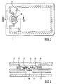
- FIG. 3 and 4 show a further embodiment of a data carrier 1.
- This differs from that shown in FIG. 2 essentially only in that the coil 7 is arranged on an inner layer 11 of the card body 2.
- This inner layer of the card body also has a corresponding opening 3 for receiving the module 6.
- the contact elements 5 of the module are preferably cranked in this embodiment, this allows a simple implementation of the electrically conductive connection with the terminals 8 of the coil.
- This embodiment has the advantage that the inner layers 11, which form the card inlay of the data carrier, can be prepared for mounting the coil and module independently of the printing process of the cover layers 10 of the data carrier.
- the data carrier was preferably manufactured in the laminating technology.
- other techniques such as injection molding or assembly technology, can also be used. These techniques are familiar to the person skilled in the art and are therefore only briefly explained in the exemplary embodiments below.
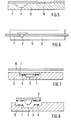
- FIG. 5 shows a highly schematic view of the semifinished product already shown in cross section in FIG. 2, which comprises the card body layer 10 with the coil 7 arranged thereon, the connections of which are electrically conductively connected to the contact elements of the module 6.
- This semi-finished product can e.g. B. also mounted on an injection molded card body part 12 which is provided with a corresponding recess for receiving the module and connected to the card body part in a known manner.
- Fig. 6 shows a highly schematic of the card inlay 11 already shown in Fig. 4 with a module 6 and a coil 7.
- This separately manufactured semi-finished product can, for. B. can also be processed in injection molding technology.
- the card insert with module and coil is introduced into an injection mold 15 in a known manner and overmolded with a plastic material which then forms the card body part 12.
- the module 7 schematically shows an injection molded card body part 12 with a two-stage recess 3, the connections 8 of the coil 7 being freely accessible on the shoulder regions of the recess.
- the module 6 can be installed in the recess 3 of the card body part 12 in a simple manner, for example in the known assembly technology, the electrically conductive connection of the coil connections to the Contact elements of the module is easy to implement.
- a printed cover layer 10 can be connected to the injection-molded card body part 12.
- the hybrid module 6 shows a hybrid module 6 which, in addition to the coil 7, has outer contact surfaces 9 which are used for the contacting energy supply and / or the data exchange.
- the hybrid module 6 can also be installed in a simple manner in the known assembly technology in a recess 3 provided for this purpose in the injection-molded card body part 12.
- a pressure-sensitive adhesive layer or a thermally activated adhesive layer can be used for module assembly.
- the application of a printed cover layer shown in FIG. 7 can be omitted here since the desired printed image is already taken into account when the card body is injection molded. In this case, the card body then only consists of one layer.
Abstract
Description
- Die Erfindung betrifft einen Datenträger gemäß dem Oberbegriff des Anspruchs 1. Ferner betrifft die Erfindung ein Verfahren zur Herstellung eines Datenträgers.
- Datenträger mit integrierten Schaltkreisen werden in Form von Kreditkarten, Bankkarten, Barzahlungskarten und dergleichen in den verschiedensten Dienstleistungssektoren, beispielsweise im bargeldlosen Zahlungsverkehr oder im innerbetrieblichen Bereich, als Zugangsberechtigung eingesetzt. Bei einem Großteil dieser Datenträger erfolgt die Energieversorgung und/oder der Datenaustausch mit externen Geräten berührend über die äußeren Kontaktflächen eines elektronischen Moduls. Da bei diesen Datenträgern nach dem Stand der Technik die Kontaktflächen zum Anschluß der Datenträger an eine Lese/Schreibeinrichtung freiliegen, besteht die Gefahr einer Verschmutzung der Kontaktflächen, wodurch in Folge einer schlechten Kontaktierung eine fehlerhafte Datenübertragung zwischen dem Datenträger und der betreffenden Lese/Schreibeinrichtung des Terminals auftreten kann. Unabhängig davon kann eine fehlerhafte Datenübertragung auch aufgrund einer fehlerhaften Positionierung der Kontaktflächen in der Lese-/Schreibeinrichtung des Terminals auftreten. Zur Vermeidung der o.g. Nachteile sind aus dem Stand der Technik bereits Datenträger mit kontaktloser, z. B. induktiver Kopplung, bekannt.
- Aus der EP-A1 0 376 062 ist z. B. ein elektronisches Modul und ein Verfahren zur Herstellung des Moduls bekannt. Das bekannte Modul beinhaltet einen isolierenden Trägerfilm, einen Chip mit integriertem Schaltkreis, der wenigstens zwei Verbindungsanschlüsse aufweist und auf dem Trägerfilm angeordnet ist. Auf der gleichen Seite des Trägerfilms des Moduls ist eine Spule angeordnet. Die Spule, welche Bestandteil des Moduls ist, ermöglicht hierbei die induktive Kopplung zwischen dem Modul und einem externen Gerät. Die Spule ist als ringförmige, drahtgewickelte Spule ausgeführt, die einen Raum umgibt, in dem der Chip und die die Anschlüsse des Chips mit den Anschlüssen der Spule elektrisch leitend verbindenden Elemente komplett untergebracht sind und der anschließend mit einer elektrisch isolierenden und gehärteten klebenden Masse gefüllt ist. Das bekannte Modul wird nach seiner Fertigstellung dann in eine Karte eingebaut, wobei die Spule einen wirksamen Schutz des Chips und der elektrisch leitenden Verbindungselemente gegen Spannungen, denen diese Karte beim Gebrauch ausgesetzt ist, gewährleistet.
- Durch die Anordnung der Spule auf dem Modul ist zwar einerseits ein guter Schutz für den Chip erreicht, andererseits bringt es dieser spezielle Aufbau eines Moduls mit sich, daß zur Herstellung eines Datenträgers mit kontaktloser Kopplung speziell aufgebaute Module verwendet werden müssen. Dies hat den Nachteil, daß zur Fertigung der Module ein spezielles Verfahren benötigt wird bzw. spezielle Werkzeuge bereitgestellt werden müssen. Darüber hinaus können bedingt durch die spezielle Fertigung dieser Module herkömmliche, d. h. Module ohne Spule für die Herstellung eines Datenträgers mit kontaktloser Kopplung nicht verwendet werden. Schließlich können bei kleinen Auflagen von Datenträgern mit kontaktloser Kopplung mit einem speziell hergestellten Modul hohe Kosten entstehen, da dieses gesondert gefertigt werden muß. Dies alles bedeutet, daß durch diese speziellen Module die Flexibilität bei der Herstellung von Datenträgern mit kontaktloser Kopplung beeinträchtigt ist.
- Der Erfindung liegt somit die Aufgabe zugrunde, einen Datenträger mit kontaktloser Kopplung vorzuschlagen, der einfacher herstellbar ist.
- Die Aufgabe wird durch die in den nebengeordneten Ansprüchen angegebenen Merkmale gelöst.
- Der Grundgedanke der Erfindung besteht in der Entkopplung von Modul und Spule, wobei das Modul in an sich bekannter Weise separat hergestellt werden kann und die Spule unabhängig von dem Modul gefertigt und auf einer Schicht des Kartenkörpers aufgebracht wird.
- Die Spule kann beispielsweise auf einer Deckschicht oder auf einer inneren Schicht eines mehrschichtig aufgebauten Kartenkörpers oder auf einem spritzgegossenen Kartenkörperteil angeordnet werden. Die Spule kann z. B. drahtgewickelt oder auch als elektrisch leitende Schicht im Siebdruckverfahren z. B. mittels eines elektrisch leitenden Klebers auf die Kartenkörperschicht aufgedruckt werden. Die Spule kann auch alternativ aus einer Metallfolie gestanzt oder aus einer elektrisch leitend beschichteten Kunststoffolie geätzt und auf die Kartenkörperschicht aufgeklebt werden. Weiter ist es auch möglich, daß die Spule in Form einer elektrisch leitenden Schicht im Heißprägeverfahren in die Kartenkörperschicht geprägt wird. Vorzugsweise ist die Spule als Flachspule ausgebildet, wobei die Anschlüsse der Spule und die Kontaktelemente des Moduls bezüglich der Lage und Position im Kartenkörper in bezug aufeinander normiert sind, beispielsweise einander direkt gegenüber angeordnet sind, wodurch eine einfache elektrisch leitende Verbindung zwischen den Anschlüssen der Spule und denen des Moduls hergestellt werden kann. Dies kann beispielsweise mit Hilfe eines elektrisch leitenden Klebers oder auch mittels Löten oder anderer gängiger Techniken, die dem Fachmann bekannt sind, erfolgen. Abschließend sei bemerkt, daß das Modul auch als Hybridmodul ausgeführt sein kann, das zusätzlich äußere Kontaktflächen zur berührenden Kopplung mit externen Geraten aufweist.
- Die mit der Erfindung erzielten Vorteile bestehen insbesondere darin, daß die in herkömmlicher Weise hergestellten Module, d. h. Module ohne Spulen, verwendbar sind, wodurch die Herstellung von Datenträgern mit kontaktloser Kopplung flexibler gestaltet werden kann. Dadurch ist keine nennenswerte Änderung bei der bisherigen Modulherstellung notwendig, so daß keine speziellen neuen Werkzeuge und auch kein neues Verfahren zur Herstellung der Module benötigt wird. Darüber hinaus ermöglicht die Erfindung aufgrund der Anordnung der Spule auf einer Kartenkörperschicht auch eine hohe Flexibilität bei der Auslegung der Spule, beispielsweise hinsichtlich der benötigten Induktivität, z. B. bei der Windungszahl, bei der aktiven Spulenfläche bzw. dem Drahtdurchmesser etc. und auch eine hohe Flexibilität bei der Auswahl der Technik, in der die Spule auf der Kartenkörperschicht realisiert wird. Darüber hinaus ermöglicht die Erfindung eine einfache Verbindung des Moduls mit der Spule, insbesondere dann, wenn die Spulenanschlüsse und die Kontaktelemente des Moduls, die mit den Spulenanschlüssen elektrisch verbunden werden, hinsichtlich der Lage und Position im Kartenkörper standardisiert sind. Auch kann der Aufbau des Moduls bis auf die Lage und Position der Kontaktelemente frei gewählt werden, so können beispielsweise die Kontaktelemente des Moduls aus einem elektrisch leitend beschichteten Trägerfilm oder in der Leadframe-Technik aus einem Metallband durch entsprechendes Stanzen erhalten werden. Der integrierte Schaltkreis kann hierbei z. B. mit Hilfe eines Klebers auf einem zentralen Bereich des gestanzten Leiterrahmens aufgeklebt werden. Die elektrisch leitende Verbindung des integrierten Schaltkreises mit den Kontaktelementen des Moduls kann z. B. in bekannter Weise per wire-bonding- oder in der sogenannten TAB-Technik erfolgen. Diese Techniken und die in diesem Zusammenhang unterschiedlichen Ausgestaltungen der Module sind dem Fachmann geläufig.
- Weitere Eigenschaften und Vorteile der Erfindung ergeben sich aus der nachfolgenden Beschreibung verschiedener Ausführungsbeispiele, die anhand der Zeichnungen näher erläutert sind.
- Weitere Ausführungsformen und Vorteile der Erfindung ergeben sich aus den Unteransprüchen sowie den Zeichnungen. Darin zeigen:
- Fig. 1
- einen Datenträger in der Aufsicht, wobei das Modul und ein Teil der Spule als Ausschnitt ohne obere Deckschicht dargestellt sind,
- Fig. 2
- den Ausschnitt des Datenträgers gemäß Fig. 1 in einer Schnittdarstellung,
- Fig. 3
- die Aufsicht auf ein weiteres Ausführungsbeispiel eines Datenträgers, wobei das Modul und ein Teil der Spule als Ausschnitt dargestellt sind,
- Fig. 4
- den Ausschnitt des Datenträgers gemäß Fig. 3 in einer Schnittdarstellung,
- Fig. 5
- ein weiteres Ausführungsbeispiel mit spritzgegossenem Kartenkörperteil,
- Fig. 6
- eine Spritzgußform mit eingelegtem Karteninlett,
- Fig. 7
- ein Hybridmodul und einen Kartenkörperteil mit Spule,
- Fig. 8
- ein kontaktloses Modul mit zugehörigem Kartenkörperteil und Spule.
- Fig. 1 zeigt einen Datenträger 1 umfassend einen Kartenkörper 2 mit einer darauf angeordneten Spule 7, die elektrisch leitend mit einem Modul 6 verbunden ist.
- Fig. 2 zeigt vergrößert und nicht maßstabsgetreu einen Querschnitt entlang der in Fig. 1 strichliert eingezeichneten Linie innerhalb des Ausschnitts, der das Modul, einen Teil des Kartenkörpers und der Spule umfaßt. Das Modul 6 umfaßt wenigstens einen integrierten Schaltkreis 4 mit zwei Anschlüssen, die elektrisch leitend mit den Kontaktelementen 5 des Moduls verbunden sind. Das in Fig. 2 gezeigte Modul besteht z. B. aus einem Trägerfilm aus Kapton, der auf einer Seite die Kontaktelemente 5 aufweist. Der Trägerfilm weist in bekannter Weise entsprechend positionierte Fenster zur Aufnahme des integrierten Schaltkreises und zur Hindurchführung der Leiterdrähte vom Schaltkreis zu den Kontaktelementen auf. Zum Schutz vor mechanischen Belastungen können der integrierte Schaltkreis und die Leiterdrähte mit einer Gußmasse vergossen werden. Bei dem hier gezeigten Ausführungsbeispiel eines Moduls sind die Kontaktelemente als elektrisch leitende Beschichtung auf dem Trägerfilm aufgebracht, die dann z. B. per wire-bonding mit den Anschlüssen des integrierten Schaltkreises verbunden werden.
- Der in Fig. 2 gezeigte Datenträger wird z. B. in der dem Fachmann geläufigen Laminiertechnik hergestellt, wobei das zuvor separat hergestellte Modul ohne Spule in einen mehrschichtig aufgebauten Kartenkörper einlaminiert wird. Der mehrschichtige Kartenkörper 2 umfaßt jeweils eine obere und untere Deckschicht 10 sowie wenigstens eine innere Kartenschicht 11, die zur Aufnahme des Moduls eine entsprechende Öffnung 3 aufweist. Die Außenflächen der Deckschichten 10 sind in der Regel mit einem Aufdruck versehen. Auf einer der Innenflächen der Deckschichten 10, in diesem Ausführungsbeispiel der oberen Deckschicht, ist eine Spule 7 angeordnet, die mit der Kartenkörperschicht 10 ein Halbzeug bildet. Die Spulenanschlüsse 8 sind derart positioniert, daß sie den Kontaktelementen 5 des Moduls 6 direkt gegenüber angeordnet sind. Dies erlaubt eine einfache elektrisch leitende Verbindung der Kontaktelemente mit den Spulenanschlüssen. Die elektrisch leitende Verbindung kann z. B. mit Hilfe eines elektrisch leitenden Klebers erzielt werden. Die Spule 7 kann z. B. auf eine Kartenkörperschicht im Siebdruckverfahren mittels eines elektrisch leitenden Klebers aufgedruckt werden oder in Form einer elektrisch leitenden Beschichtung im Heißprägeverfahren auf die Kartenkörperschicht aufgebracht werden. Alternativ hierzu kann die Spule 7 auch aus einer Metallfolie oder einer elektrisch leitend beschichteten Kunststoffolie ausgestanzt und auf einer Schicht des Kartenkörpers angeordnet werden. Die Spule kann auch als drahtgewickelte fertige Spule ohne Kern, z. B. mit Hilfe eines Klebers, auf der Kartenkörperschicht befestigt werden.
- Fig. 3 und 4 zeigen ein weiteres Ausführungsbeispiel eines Datenträgers 1. Dieser unterscheidet sich von dem in Fig. 2 gezeigten im wesentlichen nur dadurch, daß die Spule 7 auf einer inneren Schicht 11 des Kartenkörpers 2 angeordnet ist. Diese innere Schicht des Kartenkörpers weist ebenfalls eine entsprechende Öffnung 3 zur Aufnahme des Moduls 6 auf. Die Kontaktelemente 5 des Moduls sind bei dieser Ausführungsform vorzugsweise gekröpft, dies erlaubt eine einfache Realisierung der elektrisch leitenden Verbindung mit den Anschlüssen 8 der Spule. Diese Ausführungsform hat den Vorteil, daß die inneren Schichten 11, die das Karteninlett des Datenträgers bilden, unabhängig vom Druckvorgang der Deckschichten 10 des Datenträgers zur Montage von Spule und Modul vorbereitet werden können. In den bisher beschriebenen Ausführungsbeispielen wurde der Datenträger vorzugsweise in der Laminiertechnik hergestellt. Selbstverständlich können auch andere Techniken, wie beispielsweise die Spritzgußtechnik oder die Montagetechnik, zum Einsatz kommen. Diese Techniken sind dem Fachmann geläufig und werden daher in den nachfolgenden Ausführungsbeispielen nur kurz erläutert.
- Fig. 5 zeigt stark schematisiert das bereits in Fig. 2 im Querschnitt dargestellte Halbzeug, welches die Kartenkörperschicht 10 mit darauf angeordneter Spule 7 umfaßt, deren Anschlüsse elektrisch leitend mit den Kontaktelementen des Moduls 6 elektrisch leitend verbunden sind. Dieses Halbzeug kann z. B. auch auf einen spritzgegossenen Kartenkörperteil 12, der mit einer entsprechenden Aussparung zur Aufnahme des Moduls versehen ist, montiert und mit dem Kartenkörperteil in bekannter Weise verbunden werden.
- Fig. 6 zeigt stark schematisiert das bereits in Fig. 4 dargestellte Karteninlett 11 mit einem Modul 6 und einer Spule 7. Dieses separat hergestellte Halbzeug kann z. B. auch in der Spitzgußtechnik weiterverarbeitet werden. Dazu wird das Karteninlett mit Modul und Spule in bekannter Weise in eine Spritzgußform 15 eingeführt und mit einem Kunststoffmaterial umspritzt, das dann den Kartenkörperteil 12 bildet.
- Fig. 7 zeigt schematisiert ein spritzgegossenes Kartenkörperteil 12 mit einer zweistufigen Aussparung 3, wobei auf den Schulterbereichen der Aussparung die Anschlüsse 8 der Spule 7 frei zugänglich angeordnet sind. Dadurch kann das Modul 6 beispielsweise in der bekannten Montagetechnik in einfacher Weise in die Aussparung 3 des Kartenkörperteils 12 eingebaut werden, wobei die elektrisch leitende Verbindung der Spulenanschlüsse mit den Kontaktelementen des Moduls einfach realisierbar ist. Anschließend kann beispielsweise mit Hilfe einer Klebeschicht eine bedruckte Deckschicht 10 mit dem spritzgegossenen Kartenkörperteil 12 verbunden werden.
- Fig. 8 zeigt ein Hybridmodul 6, welches zusätzlich zu der Spule 7 äußere Kontaktflächen 9 aufweist, die der berührenden Energieversorgung und/oder dem Datenaustausch dienen. Das Hybridmodul 6 kann ebenfalls in einfacher Weise in der bekannten Montagetechnik in eine dafür vorgesehene Aussparung 3 des spritzgegossenen Kartenkörperteils 12 eingebaut werden. Zur Modulmontage kann beispielsweise eine Haftklebeschicht oder eine thermoaktivierbare Klebeschicht verwendet werden. Das in Fig. 7 gezeigte Aufbringen einer bedruckten Deckschicht kann hier entfallen, da das gewünschte Druckbild bereits beim Spritzgießen des Kartenkörpers mitberücksichtigt wird. In diesem Fall besteht der Kartenkörper dann nur noch aus einer Schicht.
Claims (10)
- Datenträger (1), mit einem kartenförmigen Körper (2), bestehend aus einer oder mehreren Schichten, einem integrierten Schaltkreis (4) sowie wenigstens einer Spule (7), die der Energieversorgung und/oder dem Datenaustausch des integrierten Schaltkreises mit externen Geräten dient, dadurch gekennzeichnet, daß ein an sich bekanntes Modul (6), welches den integrierten Schaltkreis (4) und wenigstens zwei Kontaktelemente (5) aufweist, über die genannten Kontaktelemente mit den Anschlüssen (8) der separat auf einer Schicht des Kartenkörpers (2) angeordneten Spule (7) elektrisch leitend verbunden ist.
- Datenträger nach Anspruch 1, dadurch gekennzeichnet, daß die Spule (7) auf einer Deckschicht (10) oder auf einer inneren Schicht (11) des Kartenkörpers (2) oder auf einem spritzgegossenen Kartenkörperteil (12) angeordnet ist.
- Datenträger nach Anspruch 2, dadurch gekennzeichnet, daß die Spule (7) als Flachspule ausgebildet ist, die als fertige drahtgewickelte Spule auf einer isolierenden Schicht des Kartenkörpers aufgeklebt oder als elektrisch leitende Schicht auf einer isolierenden Schicht des Kartenkörpers aufgedruckt oder im Heißprägeverfahren in die Kartenkörperschicht geprägt ist oder aus einer Metallfolie oder einer elektrisch leitend beschichteten Kunststoffolie gestanzt und auf einer Schicht des Kartenkörpers angeordnet ist.
- Datenträger nach Anspruch 2, dadurch gekennzeichnet, daß die Spule (7) sich im wesentlichen über die gesamte Fläche des Kartenkörpers (2) erstreckt.
- Datenträger nach Anspruch 1, dadurch gekennzeichnet, daß die Anschlüsse (8) der Spule (7) und die Kontaktelemente (5) des Moduls (6) innerhalb der Ebene des Kartenkörpers (2) einander gegenüber angeordnet sind.
- Datenträger nach Anspruch 5, dadurch gekennzeichnet, daß die Anschlüsse (8) der Spule (7) elektrisch leitend mit den Kontaktelementen (5) des Moduls (6) verklebt sind.
- Datenträger nach Anspruch 1, dadurch gekennzeichnet, daß das Modul (6) zusätzlich äußere Kontaktflächen (9) zur berührenden Energieversorgung und/oder zum Datenaustausch mit externen Geräten aufweist.
- Verfahren zur Herstellung eines Datenträgers mit einem ein- oder mehrschichtigen Kartenkörper, einem integrierten Schaltkreis sowie wenigstens einer Spule, die der Energieversorgung und/oder dem Datenaustausch des integrierten Schaltkreises mit externen Geräten dient, dadurch gekennzeichnet, daß in an sich bekannter Weise ein Modul hergestellt wird, das den integrierten Schaltkreis und wenigstens zwei Kontaktelemente aufweist und daß separat von der Herstellung des Moduls auf einer Schicht des Kartenkörpers die Spule aufgebracht wird und daß die genannten Kontaktelemente des Moduls positioniert zu den Anschlüssen der Spule angeordnet und mit den Anschlüssen der Spule elektrisch leitend verbunden werden.
- Verfahren nach Anspruch 8, dadurch gekennzeichnet, daß die Spule auf eine Kartenkörperschicht im Siebdruckverfahren mittels eines elektrisch leitenden Klebers aufgedruckt oder die Spule aus einer Metallfolie oder einer elektrisch leitend beschichteten Kunststoffolie ausgestanzt und auf die Kartenkörperschicht aufgeklebt wird oder die Spule als elektrisch leitende Schicht im Heißprägeverfahren in die Kartenkörperschicht geprägt wird oder als drahtgewickelte Spule auf die Kartenkörperschicht aufgebracht wird.
- Verfahren nach Anspruch 8, dadurch gekennzeichnet, daß die Anschlüsse der Spule mit den Kontaktelementen des Moduls elektrisch leitend verklebt werden.
Priority Applications (1)
| Application Number | Priority Date | Filing Date | Title |
|---|---|---|---|
| EP02021127A EP1271399B1 (de) | 1994-05-11 | 1995-05-10 | Datenträger mit integriertem Schaltkreis |
Applications Claiming Priority (2)
| Application Number | Priority Date | Filing Date | Title |
|---|---|---|---|
| DE4416697 | 1994-05-11 | ||
| DE4416697A DE4416697A1 (de) | 1994-05-11 | 1994-05-11 | Datenträger mit integriertem Schaltkreis |
Related Child Applications (1)
| Application Number | Title | Priority Date | Filing Date |
|---|---|---|---|
| EP02021127A Division EP1271399B1 (de) | 1994-05-11 | 1995-05-10 | Datenträger mit integriertem Schaltkreis |
Publications (3)
| Publication Number | Publication Date |
|---|---|
| EP0682321A2 true EP0682321A2 (de) | 1995-11-15 |
| EP0682321A3 EP0682321A3 (de) | 2000-01-19 |
| EP0682321B1 EP0682321B1 (de) | 2003-04-02 |
Family
ID=6517912
Family Applications (2)
| Application Number | Title | Priority Date | Filing Date |
|---|---|---|---|
| EP95107090A Revoked EP0682321B1 (de) | 1994-05-11 | 1995-05-10 | Datenträger mit integriertem Schaltkreis und Verfahren zur Herstellung eines Datenträgers |
| EP02021127A Expired - Lifetime EP1271399B1 (de) | 1994-05-11 | 1995-05-10 | Datenträger mit integriertem Schaltkreis |
Family Applications After (1)
| Application Number | Title | Priority Date | Filing Date |
|---|---|---|---|
| EP02021127A Expired - Lifetime EP1271399B1 (de) | 1994-05-11 | 1995-05-10 | Datenträger mit integriertem Schaltkreis |
Country Status (6)
| Country | Link |
|---|---|
| US (1) | US5880934A (de) |
| EP (2) | EP0682321B1 (de) |
| JP (1) | JP3795099B2 (de) |
| AT (2) | ATE236435T1 (de) |
| DE (3) | DE4416697A1 (de) |
| ES (2) | ES2191690T3 (de) |
Cited By (62)
| Publication number | Priority date | Publication date | Assignee | Title |
|---|---|---|---|---|
| EP0737935A2 (de) * | 1995-04-13 | 1996-10-16 | Sony Chemicals Corporation | Kontaktlose Chipkarte und Herstellungsverfahren |
| WO1997005569A1 (de) * | 1995-08-01 | 1997-02-13 | Austria Card Plastikkarten Und Ausweissysteme Gesellschaft Mbh | Datenträger mit einem einen bauteil aufweisenden modul und mit einer spule und verfahren zum herstellen eines solchen datenträgers |
| WO1997005571A1 (de) * | 1995-08-01 | 1997-02-13 | Austria Card Plastikkarten Und Ausweissysteme Gesellschaft Mbh | Datenträger mit einem einen bauteil aufweisenden modul und mit einer spule und verfahren zum herstellen eines solchen datenträgers sowie modul hierfür |
| WO1997023843A1 (de) * | 1995-12-22 | 1997-07-03 | Sempac Sa | Verfahren zur herstellung einer chipkarte für kontaktlosen betrieb |
| WO1997026620A1 (de) * | 1996-01-16 | 1997-07-24 | Siemens Aktiengesellschaft | Chipkartenkörper zur herstellung einer eine spule enthaltenden chipkarte |
| EP0794508A1 (de) | 1996-03-08 | 1997-09-10 | Giesecke & Devrient GmbH | Verfahren zur Herstellung eines Datenträgers mit einem elektronischen Modul |
| FR2745931A1 (fr) * | 1996-03-08 | 1997-09-12 | Freudenberg Carl Fa | Carte a puce |
| WO1997034247A2 (de) * | 1996-03-14 | 1997-09-18 | Pav Card Gmbh | Chipkarte, verbindungsanordnung und verfahren zum herstellen einer chipkarte |
| WO1997034255A1 (de) * | 1996-03-12 | 1997-09-18 | Siemens Aktiengesellschaft | Chipkarte und verfahren zur herstellung einer chipkarte |
| EP0810547A1 (de) * | 1996-05-24 | 1997-12-03 | Giesecke & Devrient GmbH | Verfahren zur Herstellung eines kartenförmigen Datenträgers |
| DE19639902A1 (de) * | 1996-06-17 | 1997-12-18 | Fraunhofer Ges Forschung | Verfahren zur Herstellung kontaktloser Chipkarten und kontaktlose Chipkarte |
| WO1998001821A1 (de) * | 1996-07-10 | 1998-01-15 | Siemens Aktiengesellschaft | Chipkarte und verfahren zu ihrer herstellung |
| EP0822512A2 (de) * | 1996-07-31 | 1998-02-04 | ODS R. Oldenbourg Datensysteme GmbH & Co. KG | Kontaktlose Chipkarte sowie Verfahren zur Herstellung kontaktloser Chipkarten |
| FR2752077A1 (fr) * | 1996-08-02 | 1998-02-06 | Solaic Sa | Carte a circuit integre a connexion mixte et module a circuit integre correspondant |
| WO1998006063A1 (fr) * | 1996-08-02 | 1998-02-12 | Solaic | Carte a circuit integre a connexion mixte |
| DE19632813A1 (de) * | 1996-08-14 | 1998-02-19 | Siemens Ag | Chipkarten-Modul, diesen enthaltende Kombi-Chipkarte und Verfahren zu deren Herstellung |
| DE19633938A1 (de) * | 1996-08-22 | 1998-02-26 | Pav Card Gmbh | Chipkarte und Verfahren zum Herstellen einer Chipkarte |
| FR2753305A1 (fr) * | 1996-09-12 | 1998-03-13 | Schlumberger Ind Sa | Procede de fabrication d'un ensemble de modules electroniques pour cartes a memoire sans contact |
| DE19640304A1 (de) * | 1996-09-30 | 1998-04-02 | Siemens Ag | Chipmodul insbesondere zur Implantation in einen Chipkartenkörper |
| WO1998016901A1 (de) * | 1996-10-14 | 1998-04-23 | Zakel, Elke | Verfahren zum herstellen einer kontaktlosen chipkarte |
| WO1998020450A1 (de) * | 1996-11-01 | 1998-05-14 | Austria Card Gmbh | Kontaktlose chipkarte mit transponderspule |
| DE19637306C1 (de) * | 1996-09-13 | 1998-05-20 | Orga Kartensysteme Gmbh | Verfahren zur Herstellung einer Chipkarte |
| WO1998022907A1 (de) * | 1996-11-19 | 1998-05-28 | Pav Card Gmbh | Verfahren zum herstellen einer chipkarte |
| WO1998024057A1 (fr) * | 1996-11-29 | 1998-06-04 | Schlumberger Systemes | Carte a memoire du type sans contact |
| WO1998033143A1 (de) * | 1997-01-28 | 1998-07-30 | Siemens Aktiengesellschaft | Trägerelement zum einbau in kombi-chipkarten und kombi-chipkarte |
| WO1998034194A1 (de) * | 1997-02-03 | 1998-08-06 | Giesecke & Devrient Gmbh | Modular aufgebauter, elektronischer datenträger |
| EP0869453A2 (de) * | 1997-03-13 | 1998-10-07 | Orga Kartensysteme GmbH | Verfahren zur Herstellung einer Chipkarte |
| WO1998049653A1 (en) * | 1997-05-01 | 1998-11-05 | Micron Communications, Inc. | Methods for forming integrated circuits within substrates, and embedded circuits |
| WO1998052154A1 (de) * | 1997-05-14 | 1998-11-19 | Meinen, Ziegel & Co. Gmbh | Verfahren und vorrichtung zur herstellung von chipkarten |
| DE19733777A1 (de) * | 1997-07-28 | 1999-02-04 | Wendisch Karl Heinz | Chipmodul, Modul und Verfahren zur Herstellung eines Moduls sowie Chipkarte |
| FR2769390A1 (fr) * | 1997-10-08 | 1999-04-09 | Gemplus Card Int | Procede de fabrication de cartes a puce aptes a assurer un fonctionnement a contact et sans contact, et de cartes a puce sans contact |
| FR2769389A1 (fr) * | 1997-10-07 | 1999-04-09 | Rue Cartes Et Systemes De | Carte a microcircuit combinant des plages de contact exterieur et une antenne, et procede de fabrication d'une telle carte |
| EP0913711A1 (de) * | 1997-10-29 | 1999-05-06 | Meto International GmbH | Identifizierungselement und Verfahren zu seiner Herstellung |
| WO1999023606A1 (de) * | 1996-06-17 | 1999-05-14 | Smart Pac Gmbh Technology Services | Verfahren zur herstellung kontaktloser chipkarten und kontaktlose chipkarte |
| DE19805282A1 (de) * | 1998-02-10 | 1999-08-19 | Siemens Ag | Flächiger Träger mit einer Anzeigeeinrichtung |
| WO1999050792A1 (en) * | 1998-03-27 | 1999-10-07 | Koninklijke Philips Electronics N.V. | Data carrier having an implanted module based on a metal lead frame |
| US6031242A (en) * | 1998-01-23 | 2000-02-29 | Zevatech, Inc. | Semiconductor die in-flight registration and orientation method and apparatus |
| AU718414B2 (en) * | 1996-11-04 | 2000-04-13 | Meto International Gmbh | Identification element and method of manufacturing the same |
| US6077022A (en) * | 1997-02-18 | 2000-06-20 | Zevatech Trading Ag | Placement machine and a method to control a placement machine |
| FR2787609A1 (fr) * | 1998-12-21 | 2000-06-23 | Gemplus Card Int | Procede de fabrication de carte a puce sans contact |
| US6081025A (en) * | 1995-08-01 | 2000-06-27 | Austria Card Plastikkarten | Data carrier with a component-containing module and with a coil, method of producing such a data carrier and module therefor |
| WO2000042569A1 (en) * | 1999-01-13 | 2000-07-20 | Brady Worldwide, Inc. | Laminate rfid label and method of manufacture |
| WO2000043952A1 (en) * | 1999-01-22 | 2000-07-27 | Intermec Ip Corp. | Rfid transponder |
| US6095424A (en) * | 1995-08-01 | 2000-08-01 | Austria Card Plasikkarten Und Ausweissysteme Gesellschaft M.B.H. | Card-shaped data carrier for contactless uses, having a component and having a transmission device for the contactless uses, and method of manufacturing such card-shaped data carriers, as well as a module therefor |
| US6135339A (en) * | 1998-01-26 | 2000-10-24 | Esec Sa | Ultrasonic transducer with a flange for mounting on an ultrasonic welding device, in particular on a wire bonder |
| WO2000068994A1 (de) | 1999-05-05 | 2000-11-16 | David Finn | Chipträger fur ein chipmodul und verfahren zur herstellung des chipmoduls |
| US6157870A (en) * | 1997-02-18 | 2000-12-05 | Zevatech Trading Ag | Apparatus supplying components to a placement machine with splice sensor |
| US6173898B1 (en) | 1998-05-11 | 2001-01-16 | Schlumberger Systemes | Memory card of the contactless type |
| US6185815B1 (en) | 1997-12-07 | 2001-02-13 | Esec Sa | Semiconductor mounting apparatus with a chip gripper travelling back and forth |
| DE19941637A1 (de) * | 1999-09-01 | 2001-03-08 | Orga Kartensysteme Gmbh | Chipkarte und Verfahren zur Herstellung einer Chipkarte |
| WO2001073800A1 (de) * | 2000-03-31 | 2001-10-04 | Interlock Ag | Verfahren zur herstellung eines etiketts oder einer chipkarte, vorrichtung zur durchführung des verfahrens und danach hergestelltes etikett oder chipkarte |
| WO2002063553A1 (fr) * | 2001-02-05 | 2002-08-15 | Gemplus Gmbh | Element de couplage pour carte a puce a double interface |
| WO2002091292A1 (de) * | 2001-05-09 | 2002-11-14 | Giesecke & Devrient Gmbh | Verfahren und halbzeug zur herstellung einer chipkarte mit spule |
| EP0689165B2 (de) † | 1994-06-22 | 2003-01-29 | SCHLUMBERGER Systèmes | Kontaktlose Speicherkarte mit IC-Modul |
| DE19634473C2 (de) * | 1996-07-11 | 2003-06-26 | David Finn | Verfahren zur Herstellung einer Chipkarte |
| US6651891B1 (en) | 1997-11-04 | 2003-11-25 | Elke Zakel | Method for producing contactless chip cards and corresponding contactless chip card |
| US7158031B2 (en) | 1992-08-12 | 2007-01-02 | Micron Technology, Inc. | Thin, flexible, RFID label and system for use |
| EP1739596A1 (de) * | 2005-06-21 | 2007-01-03 | VisionCard PersonalisierungsgmbH | Karte und Herstellungsverfahren |
| EP1873691A3 (de) * | 2006-06-30 | 2008-09-03 | Fujitsu Limited | Verfahren zur Herstellung von RFID-Etiketts und RFID-Etiketts |
| US7777317B2 (en) | 2005-12-20 | 2010-08-17 | Assa Abloy Identification Technologies Austria GmbH (Austria) | Card and manufacturing method |
| US7948382B2 (en) | 1997-08-20 | 2011-05-24 | Round Rock Research, Llc | Electronic communication devices, methods of forming electrical communication devices, and communications methods |
| CN102971155A (zh) * | 2010-07-16 | 2013-03-13 | 诺瓦利亚公司 | 电子装置 |
Families Citing this family (74)
| Publication number | Priority date | Publication date | Assignee | Title |
|---|---|---|---|---|
| DE4443980C2 (de) * | 1994-12-11 | 1997-07-17 | Angewandte Digital Elektronik | Verfahren zur Herstellung von Chipkarten und Chipkarte hergestellt nach diesem Verfahren |
| DE19527359A1 (de) * | 1995-07-26 | 1997-02-13 | Giesecke & Devrient Gmbh | Schaltungseinheit und Verfahren zur Herstellung einer Schaltungseinheit |
| DE19529640A1 (de) * | 1995-08-11 | 1997-02-13 | Giesecke & Devrient Gmbh | Spulenelement für einen Datenträger mit integriertem Schaltkreis und nichtberührender Kopplung |
| DE19543426C1 (de) * | 1995-11-21 | 1997-05-07 | Siemens Ag | Kontaktlose Chipkarte und Verfahren zur Herstellung derselben |
| DE19604774A1 (de) * | 1996-02-09 | 1997-08-14 | Siemens Ag | Kunststoffträger mit Induktionsspule |
| DE19654902C2 (de) * | 1996-03-15 | 2000-02-03 | David Finn | Chipkarte |
| DE19610507C2 (de) * | 1996-03-15 | 1997-12-04 | David Finn | Chipkarte |
| DE19613635A1 (de) * | 1996-04-04 | 1997-10-09 | Winter Wertdruck Gmbh | Verfahren zum Herstellen eines Datenträgers sowie Datenträger |
| DE19632113C1 (de) * | 1996-08-08 | 1998-02-19 | Siemens Ag | Chipkarte, Verfahren zur Herstellung einer Chipkarte und Halbleiterchip zur Verwendung in einer Chipkarte |
| DE19632814A1 (de) * | 1996-08-14 | 1998-02-19 | Siemens Ag | Kombikarte und Verfahren zu ihrer Herstellung |
| DE19641406C2 (de) * | 1996-10-08 | 2001-03-08 | Pav Card Gmbh | Chipkarte |
| FR2756955B1 (fr) * | 1996-12-11 | 1999-01-08 | Schlumberger Ind Sa | Procede de realisation d'un circuit electronique pour une carte a memoire sans contact |
| DE19703057A1 (de) * | 1996-12-20 | 1998-07-02 | Siemens Ag | Trägerelement zum Einbau in Kombi-Chipkarten und Kombi-Chipkarte |
| DE29706016U1 (de) * | 1997-04-04 | 1998-08-06 | Telbus Ges Fuer Elektronische | Elektronisches Gerät, insbesondere Chipkarte mit Nietverbindung |
| DE19716342C2 (de) * | 1997-04-18 | 1999-02-25 | Pav Card Gmbh | Verfahren zur Herstellung einer Chipkarte |
| JPH1111055A (ja) * | 1997-06-20 | 1999-01-19 | Toshiba Corp | 無線モジュール及び無線カード |
| JPH1131784A (ja) * | 1997-07-10 | 1999-02-02 | Rohm Co Ltd | 非接触icカード |
| DE19732644C1 (de) * | 1997-07-29 | 1998-11-12 | Siemens Ag | Verfahren zur Herstellung einer Chipkarte für kontaktlose Daten- und/oder Energieübertragung sowie Chipkarte |
| EP0905657B1 (de) | 1997-09-23 | 2003-05-28 | STMicroelectronics S.r.l. | Banknote mit einer integrierten Schaltung |
| DE19742268C1 (de) * | 1997-09-25 | 1999-06-02 | Orga Kartensysteme Gmbh | Verfahren zur Ermittlung des Lageversatzes von mehrlagigen Verbundstrukturen |
| JPH11143616A (ja) | 1997-11-10 | 1999-05-28 | Sega Enterp Ltd | 文字通信装置 |
| US6551449B2 (en) | 1997-11-26 | 2003-04-22 | Hitachi, Ltd. | Thin electronic circuit component and method and apparatus for producing the same |
| JPH11161760A (ja) * | 1997-11-26 | 1999-06-18 | Hitachi Ltd | 薄型電子回路部品及びその製造方法及びその製造装置 |
| US6208019B1 (en) * | 1998-03-13 | 2001-03-27 | Kabushiki Kaisha Toshiba | Ultra-thin card-type semiconductor device having an embredded semiconductor element in a space provided therein |
| DE19811577A1 (de) * | 1998-03-17 | 1999-09-23 | Siemens Ag | Chipkarte mit Wickelspule |
| DE19846237A1 (de) * | 1998-10-07 | 2000-04-13 | Fraunhofer Ges Forschung | Verfahren zur Herstellung eines Mikrotransponders |
| DE19932960C2 (de) * | 1998-10-08 | 2002-09-12 | Pav Card Gmbh | Verfahren zur Herstellung eines Chipkartenmoduls, Positioniervorrichtung zur Durchführung eines derartigen Verfahrens und Positionierverfahren |
| US6404643B1 (en) * | 1998-10-15 | 2002-06-11 | Amerasia International Technology, Inc. | Article having an embedded electronic device, and method of making same |
| DE19853018C1 (de) * | 1998-11-18 | 2000-04-20 | Prometron Gmbh | Verfahren zum Herstellen und Aufbringen einer gestanzten Antennenspule mit mehreren Windungen auf eine Chipkarte sowie eine nach diesem Verfahren hergestellte Chipkarte |
| US6288905B1 (en) | 1999-04-15 | 2001-09-11 | Amerasia International Technology Inc. | Contact module, as for a smart card, and method for making same |
| US6353420B1 (en) | 1999-04-28 | 2002-03-05 | Amerasia International Technology, Inc. | Wireless article including a plural-turn loop antenna |
| JP2001043336A (ja) * | 1999-07-29 | 2001-02-16 | Sony Chem Corp | Icカード |
| JP2001084343A (ja) * | 1999-09-16 | 2001-03-30 | Toshiba Corp | 非接触icカード及びicカード通信システム |
| US6421013B1 (en) | 1999-10-04 | 2002-07-16 | Amerasia International Technology, Inc. | Tamper-resistant wireless article including an antenna |
| JP3680676B2 (ja) * | 2000-02-03 | 2005-08-10 | 松下電器産業株式会社 | 非接触データキャリア |
| JP3729491B2 (ja) * | 2000-02-22 | 2005-12-21 | 東レエンジニアリング株式会社 | 非接触idカード類及びその製造方法 |
| FR2810638B1 (fr) * | 2000-06-22 | 2002-12-06 | Solvay | Palette en matiere plastique |
| US7501954B1 (en) | 2000-10-11 | 2009-03-10 | Avante International Technology, Inc. | Dual circuit RF identification tags |
| DE10058804C2 (de) * | 2000-11-27 | 2002-11-28 | Smart Pac Gmbh Technology Serv | Chipmodul sowie Chipkartenmodul zur Herstellung einer Chipkarte |
| JP2002319011A (ja) * | 2001-01-31 | 2002-10-31 | Canon Inc | 半導体装置、半導体装置の製造方法及び電子写真装置 |
| JP2002259923A (ja) * | 2001-03-05 | 2002-09-13 | Tokyo Magnetic Printing Co Ltd | 非接触icカードおよびその製造方法 |
| DE10117994A1 (de) * | 2001-04-10 | 2002-10-24 | Orga Kartensysteme Gmbh | Trägerfolie für elektronische Bauelemente zur Einlaminierung in Chipkarten |
| FR2824018B1 (fr) | 2001-04-26 | 2003-07-04 | Arjo Wiggins Sa | Couverture incorporant un dispositif d'identification radiofrequence |
| US6606247B2 (en) * | 2001-05-31 | 2003-08-12 | Alien Technology Corporation | Multi-feature-size electronic structures |
| DE10148105A1 (de) * | 2001-09-28 | 2003-04-17 | Orga Kartensysteme Gmbh | Verfahren zur Herstellung einer elektrischen Verbindung zwischen Bauelementen einer Datenträgerkarte |
| DE10148525B4 (de) * | 2001-10-01 | 2017-06-01 | Morpho Cards Gmbh | Chipkarte sowie ein Verfahren zur Herstellung einer derartigen Chipkarte |
| CN100334597C (zh) * | 2002-03-11 | 2007-08-29 | 阿鲁策株式会社 | Ic卡和读卡器 |
| US6665193B1 (en) | 2002-07-09 | 2003-12-16 | Amerasia International Technology, Inc. | Electronic circuit construction, as for a wireless RF tag |
| US7102524B2 (en) * | 2002-08-02 | 2006-09-05 | Symbol Technologies, Inc. | Die frame apparatus and method of transferring dies therewith |
| US7023347B2 (en) * | 2002-08-02 | 2006-04-04 | Symbol Technologies, Inc. | Method and system for forming a die frame and for transferring dies therewith |
| NL1022766C2 (nl) * | 2003-02-24 | 2004-09-21 | Enschede Sdu Bv | Identiteitskaart alsmede reisdocument. |
| MY148205A (en) * | 2003-05-13 | 2013-03-15 | Nagraid Sa | Process for assembling an electronic component on a substrate |
| US7276388B2 (en) * | 2003-06-12 | 2007-10-02 | Symbol Technologies, Inc. | Method, system, and apparatus for authenticating devices during assembly |
| US20050196604A1 (en) * | 2004-03-05 | 2005-09-08 | Unifoil Corporation | Metallization process and product produced thereby |
| FR2868987B1 (fr) * | 2004-04-14 | 2007-02-16 | Arjo Wiggins Secutity Sas Soc | Structure comportant un dispositif electronique, notamment pour la fabrication d'un document de securite ou de valeur |
| US20060146271A1 (en) * | 2005-01-04 | 2006-07-06 | Pennaz Thomas J | Universal display module |
| US20060225273A1 (en) * | 2005-03-29 | 2006-10-12 | Symbol Technologies, Inc. | Transferring die(s) from an intermediate surface to a substrate |
| US7599192B2 (en) * | 2005-04-11 | 2009-10-06 | Aveso, Inc. | Layered structure with printed elements |
| US7821794B2 (en) * | 2005-04-11 | 2010-10-26 | Aveso, Inc. | Layered label structure with timer |
| US20060238989A1 (en) * | 2005-04-25 | 2006-10-26 | Delaware Capital Formation, Inc. | Bonding and protective method and apparatus for RFID strap |
| EP1742173A3 (de) * | 2005-06-21 | 2007-08-22 | VisionCard PersonalisierungsgmbH | Karte und Herstellungsverfahren |
| US20070107186A1 (en) * | 2005-11-04 | 2007-05-17 | Symbol Technologies, Inc. | Method and system for high volume transfer of dies to substrates |
| EP1796024A1 (de) * | 2005-12-08 | 2007-06-13 | Assa Abloy Identification Technology Group AB | Verfahren zur Verbindung einer gedruckten Antenne mit einem RFID-Modul und mit diesem Verfahren hergestellte Einheit |
| CN100412899C (zh) * | 2006-08-21 | 2008-08-20 | 上海坤锐电子科技有限公司 | 一种用于制造射频识别电子标签的方法 |
| HK1109708A2 (en) * | 2007-04-24 | 2008-06-13 | On Track Innovations Ltd | Interface card and apparatus and process for the formation thereof |
| US8011577B2 (en) | 2007-12-24 | 2011-09-06 | Dynamics Inc. | Payment cards and devices with gift card, global integration, and magnetic stripe reader communication functionality |
| TWM362572U (en) * | 2009-04-13 | 2009-08-01 | Phytrex Technology Corp | Signal convertor |
| JP5461068B2 (ja) * | 2009-06-02 | 2014-04-02 | 株式会社日本インフォメーションシステム | 多層プリント配線板の製造方法および多層プリント配線板 |
| DE102009023848B4 (de) | 2009-06-04 | 2021-10-28 | Giesecke+Devrient Mobile Security Gmbh | Verfahren zur drucktechnischen Herstellung einer elektrischen Leiterbahn |
| FR2947392B1 (fr) * | 2009-06-29 | 2019-05-10 | Idemia France | Procede de raccordement electrique de deux organes entre eux |
| JP5408259B2 (ja) * | 2009-08-26 | 2014-02-05 | 凸版印刷株式会社 | 非接触通信媒体 |
| US20140211444A1 (en) * | 2013-01-30 | 2014-07-31 | Texas Instruments Incorporated | Discrete component assembly |
| DE102016014994A1 (de) * | 2016-12-16 | 2018-06-21 | Veridos Gmbh | Inlay für ein elektronisches Identifikationsdokument |
| FR3073307B1 (fr) * | 2017-11-08 | 2021-05-28 | Oberthur Technologies | Dispositif de securite tel qu'une carte a puce |
Citations (3)
| Publication number | Priority date | Publication date | Assignee | Title |
|---|---|---|---|---|
| WO1988008592A1 (en) * | 1987-04-27 | 1988-11-03 | Soundcraft, Inc. | Method for the manufacture of and structure of a laminated proximity card |
| DE4105869A1 (de) * | 1991-02-25 | 1992-08-27 | Edgar Schneider | Ic-karte und verfahren zu ihrer herstellung |
| EP0570062A1 (de) * | 1992-05-11 | 1993-11-18 | N.V. Nederlandsche Apparatenfabriek NEDAP | Konktaktlose elektronische Transponderkarte |
Family Cites Families (12)
| Publication number | Priority date | Publication date | Assignee | Title |
|---|---|---|---|---|
| NL8503410A (nl) * | 1985-12-11 | 1987-07-01 | Philips Nv | Inrichting voor het overdragen van informatie tussen een elektronische geheugenkaart en een dataverwerkende eenheid. |
| US4795898A (en) * | 1986-04-28 | 1989-01-03 | American Telephone And Telegraph Company | Personal memory card having a contactless interface using differential data transfer |
| FR2641102B1 (de) * | 1988-12-27 | 1991-02-22 | Ebauchesfabrik Eta Ag | |
| DE69101436T2 (de) * | 1990-04-19 | 1994-07-21 | Ake Gustafson | Verfahren zum montieren von einer spule auf eine leiterplatte. |
| DE4122049A1 (de) * | 1991-07-03 | 1993-01-07 | Gao Ges Automation Org | Verfahren zum einbau eines traegerelements |
| JP2709223B2 (ja) * | 1992-01-30 | 1998-02-04 | 三菱電機株式会社 | 非接触形携帯記憶装置 |
| FR2691563B1 (fr) * | 1992-05-19 | 1996-05-31 | Francois Droz | Carte comprenant au moins un element electronique et procede de fabrication d'une telle carte. |
| US5544014A (en) * | 1992-08-12 | 1996-08-06 | Oki Electric Industry Co., Ltd. | IC card having a built-in semiconductor integrated circuit device |
| US5361061A (en) * | 1992-10-19 | 1994-11-01 | Motorola, Inc. | Computer card data receiver having a foldable antenna |
| FR2716281B1 (fr) * | 1994-02-14 | 1996-05-03 | Gemplus Card Int | Procédé de fabrication d'une carte sans contact. |
| FR2716555B1 (fr) * | 1994-02-24 | 1996-05-15 | Gemplus Card Int | Procédé de fabrication d'une carte sans contact. |
| US5519201A (en) * | 1994-04-29 | 1996-05-21 | Us3, Inc. | Electrical interconnection for structure including electronic and/or electromagnetic devices |
-
1994
- 1994-05-11 DE DE4416697A patent/DE4416697A1/de not_active Withdrawn
-
1995
- 1995-05-10 ES ES95107090T patent/ES2191690T3/es not_active Expired - Lifetime
- 1995-05-10 EP EP95107090A patent/EP0682321B1/de not_active Revoked
- 1995-05-10 EP EP02021127A patent/EP1271399B1/de not_active Expired - Lifetime
- 1995-05-10 DE DE59511102T patent/DE59511102D1/de not_active Expired - Lifetime
- 1995-05-10 AT AT95107090T patent/ATE236435T1/de not_active IP Right Cessation
- 1995-05-10 DE DE59510611T patent/DE59510611D1/de not_active Revoked
- 1995-05-10 ES ES02021127T patent/ES2328337T3/es not_active Expired - Lifetime
- 1995-05-10 AT AT02021127T patent/ATE441160T1/de not_active IP Right Cessation
- 1995-05-11 JP JP11309495A patent/JP3795099B2/ja not_active Expired - Fee Related
-
1997
- 1997-10-29 US US08/960,500 patent/US5880934A/en not_active Expired - Lifetime
Patent Citations (3)
| Publication number | Priority date | Publication date | Assignee | Title |
|---|---|---|---|---|
| WO1988008592A1 (en) * | 1987-04-27 | 1988-11-03 | Soundcraft, Inc. | Method for the manufacture of and structure of a laminated proximity card |
| DE4105869A1 (de) * | 1991-02-25 | 1992-08-27 | Edgar Schneider | Ic-karte und verfahren zu ihrer herstellung |
| EP0570062A1 (de) * | 1992-05-11 | 1993-11-18 | N.V. Nederlandsche Apparatenfabriek NEDAP | Konktaktlose elektronische Transponderkarte |
Cited By (102)
| Publication number | Priority date | Publication date | Assignee | Title |
|---|---|---|---|---|
| US7265674B2 (en) | 1992-08-12 | 2007-09-04 | Micron Technology, Inc. | Thin flexible, RFID labels, and method and apparatus for use |
| US7158031B2 (en) | 1992-08-12 | 2007-01-02 | Micron Technology, Inc. | Thin, flexible, RFID label and system for use |
| EP0689165B2 (de) † | 1994-06-22 | 2003-01-29 | SCHLUMBERGER Systèmes | Kontaktlose Speicherkarte mit IC-Modul |
| EP0737935A3 (de) * | 1995-04-13 | 1999-12-01 | Sony Chemicals Corporation | Kontaktlose Chipkarte und Herstellungsverfahren |
| EP0737935A2 (de) * | 1995-04-13 | 1996-10-16 | Sony Chemicals Corporation | Kontaktlose Chipkarte und Herstellungsverfahren |
| WO1997005569A1 (de) * | 1995-08-01 | 1997-02-13 | Austria Card Plastikkarten Und Ausweissysteme Gesellschaft Mbh | Datenträger mit einem einen bauteil aufweisenden modul und mit einer spule und verfahren zum herstellen eines solchen datenträgers |
| WO1997005571A1 (de) * | 1995-08-01 | 1997-02-13 | Austria Card Plastikkarten Und Ausweissysteme Gesellschaft Mbh | Datenträger mit einem einen bauteil aufweisenden modul und mit einer spule und verfahren zum herstellen eines solchen datenträgers sowie modul hierfür |
| US6081025A (en) * | 1995-08-01 | 2000-06-27 | Austria Card Plastikkarten | Data carrier with a component-containing module and with a coil, method of producing such a data carrier and module therefor |
| US5996897A (en) * | 1995-08-01 | 1999-12-07 | Austria Card Plastikkarten Und Ausweissysteme Gesellschaft M.B.H | Data carrier having a module including a component and having a coil, and method of manufacturing such a data carrier |
| US5969415A (en) * | 1995-08-01 | 1999-10-19 | Austria Card Plastikkarten | Data carrier with a component-containing module and with a coil, method of producing such a data carrier and module therefor |
| US6095424A (en) * | 1995-08-01 | 2000-08-01 | Austria Card Plasikkarten Und Ausweissysteme Gesellschaft M.B.H. | Card-shaped data carrier for contactless uses, having a component and having a transmission device for the contactless uses, and method of manufacturing such card-shaped data carriers, as well as a module therefor |
| WO1997023843A1 (de) * | 1995-12-22 | 1997-07-03 | Sempac Sa | Verfahren zur herstellung einer chipkarte für kontaktlosen betrieb |
| WO1997026620A1 (de) * | 1996-01-16 | 1997-07-24 | Siemens Aktiengesellschaft | Chipkartenkörper zur herstellung einer eine spule enthaltenden chipkarte |
| FR2745931A1 (fr) * | 1996-03-08 | 1997-09-12 | Freudenberg Carl Fa | Carte a puce |
| EP0794508A1 (de) | 1996-03-08 | 1997-09-10 | Giesecke & Devrient GmbH | Verfahren zur Herstellung eines Datenträgers mit einem elektronischen Modul |
| WO1997034255A1 (de) * | 1996-03-12 | 1997-09-18 | Siemens Aktiengesellschaft | Chipkarte und verfahren zur herstellung einer chipkarte |
| US6020627A (en) * | 1996-03-12 | 2000-02-01 | Siemens Aktiengesellschaft | Chip card and method of manufacturing a chip card |
| WO1997034247A3 (de) * | 1996-03-14 | 1998-01-08 | Pav Card Gmbh | Chipkarte, verbindungsanordnung und verfahren zum herstellen einer chipkarte |
| WO1997034247A2 (de) * | 1996-03-14 | 1997-09-18 | Pav Card Gmbh | Chipkarte, verbindungsanordnung und verfahren zum herstellen einer chipkarte |
| EP0810547A1 (de) * | 1996-05-24 | 1997-12-03 | Giesecke & Devrient GmbH | Verfahren zur Herstellung eines kartenförmigen Datenträgers |
| WO1999023606A1 (de) * | 1996-06-17 | 1999-05-14 | Smart Pac Gmbh Technology Services | Verfahren zur herstellung kontaktloser chipkarten und kontaktlose chipkarte |
| DE19639902C2 (de) * | 1996-06-17 | 2001-03-01 | Elke Zakel | Verfahren zur Herstellung kontaktloser Chipkarten und kontaktlose Chipkarte |
| DE19639902A1 (de) * | 1996-06-17 | 1997-12-18 | Fraunhofer Ges Forschung | Verfahren zur Herstellung kontaktloser Chipkarten und kontaktlose Chipkarte |
| WO1998001821A1 (de) * | 1996-07-10 | 1998-01-15 | Siemens Aktiengesellschaft | Chipkarte und verfahren zu ihrer herstellung |
| DE19634473C2 (de) * | 1996-07-11 | 2003-06-26 | David Finn | Verfahren zur Herstellung einer Chipkarte |
| EP0822512A2 (de) * | 1996-07-31 | 1998-02-04 | ODS R. Oldenbourg Datensysteme GmbH & Co. KG | Kontaktlose Chipkarte sowie Verfahren zur Herstellung kontaktloser Chipkarten |
| EP0822512A3 (de) * | 1996-07-31 | 1999-01-20 | ODS R. Oldenbourg Datensysteme GmbH & Co. KG | Kontaktlose Chipkarte sowie Verfahren zur Herstellung kontaktloser Chipkarten |
| FR2752077A1 (fr) * | 1996-08-02 | 1998-02-06 | Solaic Sa | Carte a circuit integre a connexion mixte et module a circuit integre correspondant |
| WO1998006063A1 (fr) * | 1996-08-02 | 1998-02-12 | Solaic | Carte a circuit integre a connexion mixte |
| CN1116655C (zh) * | 1996-08-02 | 2003-07-30 | 施伦贝格尔体系公司 | 具有两种连接方式的集成电路卡 |
| US6301119B1 (en) | 1996-08-02 | 2001-10-09 | Schlumberger Systemes | Integrated circuit card with two connection modes |
| DE19632813A1 (de) * | 1996-08-14 | 1998-02-19 | Siemens Ag | Chipkarten-Modul, diesen enthaltende Kombi-Chipkarte und Verfahren zu deren Herstellung |
| DE19632813C2 (de) * | 1996-08-14 | 2000-11-02 | Siemens Ag | Verfahren zur Herstellung eines Chipkarten-Moduls, unter Verwendung dieses Verfahrens hergestellter Chipkarten-Modul und diesen Chipkarten-Modul enthaltende Kombi-Chipkarte |
| US6095423A (en) * | 1996-08-14 | 2000-08-01 | Siemens Aktiengesellschaft | Method of producing a smart card module, a smart card module produced by the method, and a combination smart card containing the smart card module |
| DE19633938A1 (de) * | 1996-08-22 | 1998-02-26 | Pav Card Gmbh | Chipkarte und Verfahren zum Herstellen einer Chipkarte |
| WO1998011507A1 (fr) * | 1996-09-12 | 1998-03-19 | Schlumberger Systemes | Procede de fabrication d'un ensemble de modules electroniques pour cartes a memoire sans contact |
| FR2753305A1 (fr) * | 1996-09-12 | 1998-03-13 | Schlumberger Ind Sa | Procede de fabrication d'un ensemble de modules electroniques pour cartes a memoire sans contact |
| DE19637306C1 (de) * | 1996-09-13 | 1998-05-20 | Orga Kartensysteme Gmbh | Verfahren zur Herstellung einer Chipkarte |
| US6288904B1 (en) | 1996-09-30 | 2001-09-11 | Infineon Technologies Ag | Chip module, in particular for implantation in a smart card body |
| DE19640304C2 (de) * | 1996-09-30 | 2000-10-12 | Siemens Ag | Chipmodul insbesondere zur Implantation in einen Chipkartenkörper |
| DE19640304A1 (de) * | 1996-09-30 | 1998-04-02 | Siemens Ag | Chipmodul insbesondere zur Implantation in einen Chipkartenkörper |
| WO1998016901A1 (de) * | 1996-10-14 | 1998-04-23 | Zakel, Elke | Verfahren zum herstellen einer kontaktlosen chipkarte |
| WO1998020450A1 (de) * | 1996-11-01 | 1998-05-14 | Austria Card Gmbh | Kontaktlose chipkarte mit transponderspule |
| AU718414B2 (en) * | 1996-11-04 | 2000-04-13 | Meto International Gmbh | Identification element and method of manufacturing the same |
| WO1998022907A1 (de) * | 1996-11-19 | 1998-05-28 | Pav Card Gmbh | Verfahren zum herstellen einer chipkarte |
| US6422472B1 (en) | 1996-11-29 | 2002-07-23 | Schlumberger Systems | Memory card of the contactless type |
| WO1998024057A1 (fr) * | 1996-11-29 | 1998-06-04 | Schlumberger Systemes | Carte a memoire du type sans contact |
| WO1998033143A1 (de) * | 1997-01-28 | 1998-07-30 | Siemens Aktiengesellschaft | Trägerelement zum einbau in kombi-chipkarten und kombi-chipkarte |
| WO1998034194A1 (de) * | 1997-02-03 | 1998-08-06 | Giesecke & Devrient Gmbh | Modular aufgebauter, elektronischer datenträger |
| US6157870A (en) * | 1997-02-18 | 2000-12-05 | Zevatech Trading Ag | Apparatus supplying components to a placement machine with splice sensor |
| US6077022A (en) * | 1997-02-18 | 2000-06-20 | Zevatech Trading Ag | Placement machine and a method to control a placement machine |
| EP0869453A3 (de) * | 1997-03-13 | 2002-08-07 | Orga Kartensysteme GmbH | Verfahren zur Herstellung einer Chipkarte |
| EP0869453A2 (de) * | 1997-03-13 | 1998-10-07 | Orga Kartensysteme GmbH | Verfahren zur Herstellung einer Chipkarte |
| USRE40137E1 (en) | 1997-05-01 | 2008-03-04 | Micron Technology, Inc. | Methods for forming integrated circuits within substrates |
| WO1998049653A1 (en) * | 1997-05-01 | 1998-11-05 | Micron Communications, Inc. | Methods for forming integrated circuits within substrates, and embedded circuits |
| GB2339407A (en) * | 1997-05-01 | 2000-01-26 | Micron Technology Inc | Methods for forming integrated circuits within substrates,and embedded circuits |
| GB2339407B (en) * | 1997-05-01 | 2001-12-19 | Micron Technology Inc | Methods for forming integrated circuits within substrates,and embedded circuits |
| US6329213B1 (en) | 1997-05-01 | 2001-12-11 | Micron Technology, Inc. | Methods for forming integrated circuits within substrates |
| US6271801B2 (en) | 1997-05-01 | 2001-08-07 | Micron Technology, Inc. | Embedded circuits |
| WO1998052154A1 (de) * | 1997-05-14 | 1998-11-19 | Meinen, Ziegel & Co. Gmbh | Verfahren und vorrichtung zur herstellung von chipkarten |
| DE19733777A1 (de) * | 1997-07-28 | 1999-02-04 | Wendisch Karl Heinz | Chipmodul, Modul und Verfahren zur Herstellung eines Moduls sowie Chipkarte |
| DE19733777C2 (de) * | 1997-07-28 | 2003-12-18 | Microidentt Ges Fuer Identifik | Modul und Verfahren zur Herstellung eines Moduls sowie eine Chipkarte |
| US7948382B2 (en) | 1997-08-20 | 2011-05-24 | Round Rock Research, Llc | Electronic communication devices, methods of forming electrical communication devices, and communications methods |
| FR2769389A1 (fr) * | 1997-10-07 | 1999-04-09 | Rue Cartes Et Systemes De | Carte a microcircuit combinant des plages de contact exterieur et une antenne, et procede de fabrication d'une telle carte |
| US6320753B1 (en) | 1997-10-07 | 2001-11-20 | Oberthur Card Systems Sa | Integrated circuit board combining external contact zones and an antenna, and process for manufacturing such a board |
| EP0908844A1 (de) * | 1997-10-07 | 1999-04-14 | De La Rue Cartes Et Systemes | Karte mit Mikroschaltung, welche die Strecken des externen Kontaktes und einer Antenne kombiniert und Herstellungsverfahren einer solchen Karte |
| WO1999018541A1 (fr) * | 1997-10-08 | 1999-04-15 | Gemplus S.C.A. | Procede de fabrication de cartes a puce aptes a assurer un fonctionnement a contact, et sans contact |
| FR2769390A1 (fr) * | 1997-10-08 | 1999-04-09 | Gemplus Card Int | Procede de fabrication de cartes a puce aptes a assurer un fonctionnement a contact et sans contact, et de cartes a puce sans contact |
| US7958622B1 (en) | 1997-10-08 | 2011-06-14 | Gemalto S.A. | Method for making smart cards |
| US7663564B2 (en) | 1997-10-08 | 2010-02-16 | Gemalto, S.A. | Method for making smart cards capable of operating with and without contact |
| US7740180B2 (en) | 1997-10-08 | 2010-06-22 | Gemalto, S.A. | Method for making smart cards capable of operating with and without contact |
| EP0913711A1 (de) * | 1997-10-29 | 1999-05-06 | Meto International GmbH | Identifizierungselement und Verfahren zu seiner Herstellung |
| US6651891B1 (en) | 1997-11-04 | 2003-11-25 | Elke Zakel | Method for producing contactless chip cards and corresponding contactless chip card |
| US6185815B1 (en) | 1997-12-07 | 2001-02-13 | Esec Sa | Semiconductor mounting apparatus with a chip gripper travelling back and forth |
| US6031242A (en) * | 1998-01-23 | 2000-02-29 | Zevatech, Inc. | Semiconductor die in-flight registration and orientation method and apparatus |
| US6135339A (en) * | 1998-01-26 | 2000-10-24 | Esec Sa | Ultrasonic transducer with a flange for mounting on an ultrasonic welding device, in particular on a wire bonder |
| US6414441B1 (en) | 1998-02-10 | 2002-07-02 | Infineon Technologies Ag | Flat carrier with an indicating device |
| DE19805282A1 (de) * | 1998-02-10 | 1999-08-19 | Siemens Ag | Flächiger Träger mit einer Anzeigeeinrichtung |
| WO1999050792A1 (en) * | 1998-03-27 | 1999-10-07 | Koninklijke Philips Electronics N.V. | Data carrier having an implanted module based on a metal lead frame |
| US6321993B1 (en) | 1998-03-27 | 2001-11-27 | U.S. Philips Corporation | Data carrier having an implanted module based on a metal lead frame |
| US6173898B1 (en) | 1998-05-11 | 2001-01-16 | Schlumberger Systemes | Memory card of the contactless type |
| FR2787609A1 (fr) * | 1998-12-21 | 2000-06-23 | Gemplus Card Int | Procede de fabrication de carte a puce sans contact |
| WO2000038111A1 (fr) * | 1998-12-21 | 2000-06-29 | Gemplus | Procede de fabrication de carte a puce sans contact |
| US6617676B1 (en) | 1998-12-21 | 2003-09-09 | Gemplus | Method for making a contactless chip card |
| US6429831B2 (en) | 1999-01-13 | 2002-08-06 | Brady Worldwide, Inc. | Laminate RFID label and method of manufacture |
| US6569508B2 (en) | 1999-01-13 | 2003-05-27 | Brady Worldwide, Inc. | Label having a protective cavity and method of manufacture |
| WO2000042569A1 (en) * | 1999-01-13 | 2000-07-20 | Brady Worldwide, Inc. | Laminate rfid label and method of manufacture |
| WO2000043952A1 (en) * | 1999-01-22 | 2000-07-27 | Intermec Ip Corp. | Rfid transponder |
| US7105915B1 (en) | 1999-05-05 | 2006-09-12 | David Finn | Chip carrier a chip module and method of manufacturing the chip module |
| WO2000068994A1 (de) | 1999-05-05 | 2000-11-16 | David Finn | Chipträger fur ein chipmodul und verfahren zur herstellung des chipmoduls |
| DE19941637A1 (de) * | 1999-09-01 | 2001-03-08 | Orga Kartensysteme Gmbh | Chipkarte und Verfahren zur Herstellung einer Chipkarte |
| US7047624B2 (en) | 2000-03-31 | 2006-05-23 | Interlock Ag | Method for producing a tag or a chip card having a coil antenna |
| WO2001073800A1 (de) * | 2000-03-31 | 2001-10-04 | Interlock Ag | Verfahren zur herstellung eines etiketts oder einer chipkarte, vorrichtung zur durchführung des verfahrens und danach hergestelltes etikett oder chipkarte |
| WO2002063553A1 (fr) * | 2001-02-05 | 2002-08-15 | Gemplus Gmbh | Element de couplage pour carte a puce a double interface |
| WO2002091292A1 (de) * | 2001-05-09 | 2002-11-14 | Giesecke & Devrient Gmbh | Verfahren und halbzeug zur herstellung einer chipkarte mit spule |
| US7154758B2 (en) | 2001-05-09 | 2006-12-26 | Giesecke & Devrient Gmbh | Method and semi-product for producing a chip card with a coil |
| EP1739596A1 (de) * | 2005-06-21 | 2007-01-03 | VisionCard PersonalisierungsgmbH | Karte und Herstellungsverfahren |
| US7777317B2 (en) | 2005-12-20 | 2010-08-17 | Assa Abloy Identification Technologies Austria GmbH (Austria) | Card and manufacturing method |
| EP1873691A3 (de) * | 2006-06-30 | 2008-09-03 | Fujitsu Limited | Verfahren zur Herstellung von RFID-Etiketts und RFID-Etiketts |
| US7936273B2 (en) | 2006-06-30 | 2011-05-03 | Fujitsu Limited | RFID tag manufacturing methods and RFID tags |
| CN102971155A (zh) * | 2010-07-16 | 2013-03-13 | 诺瓦利亚公司 | 电子装置 |
| CN102971155B (zh) * | 2010-07-16 | 2016-08-17 | 诺瓦利亚公司 | 电子装置 |
Also Published As
| Publication number | Publication date |
|---|---|
| US5880934A (en) | 1999-03-09 |
| DE59510611D1 (de) | 2003-05-08 |
| EP1271399A1 (de) | 2003-01-02 |
| ATE441160T1 (de) | 2009-09-15 |
| ES2328337T3 (es) | 2009-11-12 |
| DE4416697A1 (de) | 1995-11-16 |
| EP0682321A3 (de) | 2000-01-19 |
| EP0682321B1 (de) | 2003-04-02 |
| JP3795099B2 (ja) | 2006-07-12 |
| JPH0844840A (ja) | 1996-02-16 |
| ATE236435T1 (de) | 2003-04-15 |
| ES2191690T3 (es) | 2003-09-16 |
| EP1271399B1 (de) | 2009-08-26 |
| DE59511102D1 (de) | 2009-10-08 |
Similar Documents
| Publication | Publication Date | Title |
|---|---|---|
| EP0682321B1 (de) | Datenträger mit integriertem Schaltkreis und Verfahren zur Herstellung eines Datenträgers | |
| DE69730362T2 (de) | Kontaktloser elektronischer Modul für eine Karte oder ein Etikett | |
| EP0869453B1 (de) | Verfahren zur Herstellung einer Chipkarte | |
| EP0723244B1 (de) | Datenträger mit einem elektronischen Modul | |
| EP0796477B1 (de) | Folienausführung für die montage von chipkarten mit spulen | |
| EP0710919A2 (de) | Kontaktloses elektronisches Modul | |
| EP1152368B1 (de) | Chipkarte | |
| EP0902973B1 (de) | Trägerelement für einen halbleiterchip | |
| WO1998007191A1 (de) | Kombinations-chipmodul und verfahren zur herstellung eines kombinations-chipmoduls | |
| EP0996932B1 (de) | Kontaktlos betreibbarer datenträger | |
| EP0232705A2 (de) | Elektronische Datenträger und Verfahren zu seiner Herstellung | |
| DE3824870A1 (de) | System zur kontaktlosen informationsuebertragung zwischen einer ic-karte und einem kartenlese-/-schreibgeraet sowie ic-karte | |
| DE19703057A1 (de) | Trägerelement zum Einbau in Kombi-Chipkarten und Kombi-Chipkarte | |
| WO1996007982A1 (de) | Schaltungsanordnung mit einem chipkartenmodul und einer damit verbundenen spule | |
| EP0842493B1 (de) | Datenträger mit einem bauteil aufweisenden modul und mit einer spule und verfahren zum herstellen eines solchen datenträgers sowie modul hierfür | |
| EP1527413B1 (de) | Datenträger mit transponderspule | |
| DE19632117C1 (de) | Datenträger zur kontaktlosen Übertragung von elektrischen Signalen | |
| DE19609149C2 (de) | Chipkarte | |
| DE10236666A1 (de) | Verfahren zum Herstellen von Kontaktlosen und/oder gemischten Chipkarten | |
| EP1684216A1 (de) | Tragbarer Datenträger | |
| DE19733124C1 (de) | Chipkarte für kontaktlose Daten- und/oder Energieübertragung sowie Verfahren zu deren Herstellung | |
| WO1998033143A1 (de) | Trägerelement zum einbau in kombi-chipkarten und kombi-chipkarte | |
| DE10105069C2 (de) | Kopplungselement für Dual-Interface-Karte | |
| DE19733348A1 (de) | Kartenförmiger Datenträger mit einer Spule für eine kontaktlose Datenübertragung und Vorrichtung zum Wickeln einer solchen Spule | |
| DE19543426C1 (de) | Kontaktlose Chipkarte und Verfahren zur Herstellung derselben |
Legal Events
| Date | Code | Title | Description |
|---|---|---|---|
| PUAI | Public reference made under article 153(3) epc to a published international application that has entered the european phase |
Free format text: ORIGINAL CODE: 0009012 |
|
| AK | Designated contracting states |
Kind code of ref document: A2 Designated state(s): AT BE CH DE DK ES FR GB GR IE IT LI LU MC NL PT SE |
|
| PUAL | Search report despatched |
Free format text: ORIGINAL CODE: 0009013 |
|
| AK | Designated contracting states |
Kind code of ref document: A3 Designated state(s): AT BE CH DE DK ES FR GB GR IE IT LI LU MC NL PT SE |
|
| 17P | Request for examination filed |
Effective date: 20000713 |
|
| 17Q | First examination report despatched |
Effective date: 20010613 |
|
| GRAG | Despatch of communication of intention to grant |
Free format text: ORIGINAL CODE: EPIDOS AGRA |
|
| RTI1 | Title (correction) |
Free format text: RECORD CARRIER WITH INTEGRATED CIRCUIT AND PROCEDURE FOR MANUFACTURING A RECORD CARRIER |
|
| GRAG | Despatch of communication of intention to grant |
Free format text: ORIGINAL CODE: EPIDOS AGRA |
|
| GRAH | Despatch of communication of intention to grant a patent |
Free format text: ORIGINAL CODE: EPIDOS IGRA |
|
| GRAH | Despatch of communication of intention to grant a patent |
Free format text: ORIGINAL CODE: EPIDOS IGRA |
|
| GRAA | (expected) grant |
Free format text: ORIGINAL CODE: 0009210 |
|
| AK | Designated contracting states |
Designated state(s): AT BE CH DE DK ES FR GB GR IE IT LI LU MC NL PT SE |
|
| PG25 | Lapsed in a contracting state [announced via postgrant information from national office to epo] |
Ref country code: IE Free format text: LAPSE BECAUSE OF NON-PAYMENT OF DUE FEES Effective date: 20030402 |
|
| REG | Reference to a national code |
Ref country code: GB Ref legal event code: FG4D Free format text: NOT ENGLISH |
|
| REG | Reference to a national code |
Ref country code: CH Ref legal event code: EP |
|
| REG | Reference to a national code |
Ref country code: CH Ref legal event code: NV Representative=s name: PATENTANWAELTE SCHAAD, BALASS, MENZL & PARTNER AG Ref country code: IE Ref legal event code: FG4D Free format text: GERMAN |
|
| REF | Corresponds to: |
Ref document number: 59510611 Country of ref document: DE Date of ref document: 20030508 Kind code of ref document: P |
|
| PG25 | Lapsed in a contracting state [announced via postgrant information from national office to epo] |
Ref country code: LU Free format text: LAPSE BECAUSE OF NON-PAYMENT OF DUE FEES Effective date: 20030510 |
|
| PG25 | Lapsed in a contracting state [announced via postgrant information from national office to epo] |
Ref country code: MC Free format text: LAPSE BECAUSE OF NON-PAYMENT OF DUE FEES Effective date: 20030531 |
|
| PG25 | Lapsed in a contracting state [announced via postgrant information from national office to epo] |
Ref country code: PT Free format text: LAPSE BECAUSE OF FAILURE TO SUBMIT A TRANSLATION OF THE DESCRIPTION OR TO PAY THE FEE WITHIN THE PRESCRIBED TIME-LIMIT Effective date: 20030702 Ref country code: GR Free format text: LAPSE BECAUSE OF FAILURE TO SUBMIT A TRANSLATION OF THE DESCRIPTION OR TO PAY THE FEE WITHIN THE PRESCRIBED TIME-LIMIT Effective date: 20030702 Ref country code: DK Free format text: LAPSE BECAUSE OF FAILURE TO SUBMIT A TRANSLATION OF THE DESCRIPTION OR TO PAY THE FEE WITHIN THE PRESCRIBED TIME-LIMIT Effective date: 20030702 |
|
| REG | Reference to a national code |
Ref country code: SE Ref legal event code: TRGR |
|
| GBT | Gb: translation of ep patent filed (gb section 77(6)(a)/1977) |
Effective date: 20030714 |
|
| REG | Reference to a national code |
Ref country code: ES Ref legal event code: FG2A Ref document number: 2191690 Country of ref document: ES Kind code of ref document: T3 |
|
| ET | Fr: translation filed | ||
| REG | Reference to a national code |
Ref country code: IE Ref legal event code: FD4D Ref document number: 0682321E Country of ref document: IE |
|
| PLBQ | Unpublished change to opponent data |
Free format text: ORIGINAL CODE: EPIDOS OPPO |
|
| PLBI | Opposition filed |
Free format text: ORIGINAL CODE: 0009260 |
|
| PLAX | Notice of opposition and request to file observation + time limit sent |
Free format text: ORIGINAL CODE: EPIDOSNOBS2 |
|
| 26 | Opposition filed |
Opponent name: CUBIT ELECTRONICS GMBH Effective date: 20031230 |
|
| PGFP | Annual fee paid to national office [announced via postgrant information from national office to epo] |
Ref country code: ES Payment date: 20040324 Year of fee payment: 10 |
|
| NLR1 | Nl: opposition has been filed with the epo |
Opponent name: CUBIT ELECTRONICS GMBH |
|
| PLBB | Reply of patent proprietor to notice(s) of opposition received |
Free format text: ORIGINAL CODE: EPIDOSNOBS3 |
|
| PGFP | Annual fee paid to national office [announced via postgrant information from national office to epo] |
Ref country code: AT Payment date: 20050322 Year of fee payment: 11 |
|
| PLAQ | Examination of admissibility of opposition: information related to despatch of communication + time limit deleted |
Free format text: ORIGINAL CODE: EPIDOSDOPE2 |
|
| PLAR | Examination of admissibility of opposition: information related to receipt of reply deleted |
Free format text: ORIGINAL CODE: EPIDOSDOPE4 |
|
| PLBQ | Unpublished change to opponent data |
Free format text: ORIGINAL CODE: EPIDOS OPPO |
|
| PLAB | Opposition data, opponent's data or that of the opponent's representative modified |
Free format text: ORIGINAL CODE: 0009299OPPO |
|
| PGFP | Annual fee paid to national office [announced via postgrant information from national office to epo] |
Ref country code: GB Payment date: 20050425 Year of fee payment: 11 |
|
| PGFP | Annual fee paid to national office [announced via postgrant information from national office to epo] |
Ref country code: NL Payment date: 20050518 Year of fee payment: 11 |
|
| PGFP | Annual fee paid to national office [announced via postgrant information from national office to epo] |
Ref country code: FR Payment date: 20050519 Year of fee payment: 11 |
|
| RDAF | Communication despatched that patent is revoked |
Free format text: ORIGINAL CODE: EPIDOSNREV1 |
|
| PGFP | Annual fee paid to national office [announced via postgrant information from national office to epo] |
Ref country code: BE Payment date: 20050523 Year of fee payment: 11 |
|
| PGFP | Annual fee paid to national office [announced via postgrant information from national office to epo] |
Ref country code: SE Payment date: 20050524 Year of fee payment: 11 Ref country code: CH Payment date: 20050524 Year of fee payment: 11 |
|
| R26 | Opposition filed (corrected) |
Opponent name: SOKYMAT GMBH Effective date: 20031230 |
|
| PGFP | Annual fee paid to national office [announced via postgrant information from national office to epo] |
Ref country code: DE Payment date: 20050725 Year of fee payment: 11 |
|
| NLR1 | Nl: opposition has been filed with the epo |
Opponent name: SOKYMAT GMBH |
|
| APBP | Date of receipt of notice of appeal recorded |
Free format text: ORIGINAL CODE: EPIDOSNNOA2O |
|
| APAH | Appeal reference modified |
Free format text: ORIGINAL CODE: EPIDOSCREFNO |
|
| APAH | Appeal reference modified |
Free format text: ORIGINAL CODE: EPIDOSCREFNO |
|
| APAH | Appeal reference modified |
Free format text: ORIGINAL CODE: EPIDOSCREFNO |
|
| APBU | Appeal procedure closed |
Free format text: ORIGINAL CODE: EPIDOSNNOA9O |
|
| RDAG | Patent revoked |
Free format text: ORIGINAL CODE: 0009271 |
|
| STAA | Information on the status of an ep patent application or granted ep patent |
Free format text: STATUS: PATENT REVOKED |
|
| REG | Reference to a national code |
Ref country code: CH Ref legal event code: PL |
|
| 27W | Patent revoked |
Effective date: 20051026 |
|
| GBPR | Gb: patent revoked under art. 102 of the ep convention designating the uk as contracting state |
Free format text: 20051026 |
|
| NLR2 | Nl: decision of opposition |
Effective date: 20051026 |
|
| REG | Reference to a national code |
Ref country code: SE Ref legal event code: ECNC |
|
| PGFP | Annual fee paid to national office [announced via postgrant information from national office to epo] |
Ref country code: IT Payment date: 20060531 Year of fee payment: 12 |
|
| PLAB | Opposition data, opponent's data or that of the opponent's representative modified |
Free format text: ORIGINAL CODE: 0009299OPPO |