EP0674435B1 - Image sensing apparatus - Google Patents
Image sensing apparatus Download PDFInfo
- Publication number
- EP0674435B1 EP0674435B1 EP95102412A EP95102412A EP0674435B1 EP 0674435 B1 EP0674435 B1 EP 0674435B1 EP 95102412 A EP95102412 A EP 95102412A EP 95102412 A EP95102412 A EP 95102412A EP 0674435 B1 EP0674435 B1 EP 0674435B1
- Authority
- EP
- European Patent Office
- Prior art keywords
- image
- signal processing
- camera head
- image sensing
- head unit
- Prior art date
- Legal status (The legal status is an assumption and is not a legal conclusion. Google has not performed a legal analysis and makes no representation as to the accuracy of the status listed.)
- Expired - Lifetime
Links
Images


Classifications
-
- H—ELECTRICITY
- H04—ELECTRIC COMMUNICATION TECHNIQUE
- H04N—PICTORIAL COMMUNICATION, e.g. TELEVISION
- H04N23/00—Cameras or camera modules comprising electronic image sensors; Control thereof
- H04N23/60—Control of cameras or camera modules
- H04N23/66—Remote control of cameras or camera parts, e.g. by remote control devices
- H04N23/663—Remote control of cameras or camera parts, e.g. by remote control devices for controlling interchangeable camera parts based on electronic image sensor signals
-
- H—ELECTRICITY
- H04—ELECTRIC COMMUNICATION TECHNIQUE
- H04N—PICTORIAL COMMUNICATION, e.g. TELEVISION
- H04N23/00—Cameras or camera modules comprising electronic image sensors; Control thereof
Definitions
- the present invention relates to an image sensing apparatus for inputting images into computers and, more particularly, to an image sensing apparatus which directly controls various functions for inputting images using a computer.
- the video input board 420 is constructed as an expansion board to be built in a computer, and connected to the computer via computer bus 155P.
- the computer bus 155P known as ISA Bus, VL Bus, Nu Bus, or the like, includes address lines, data lines, an interruption line, a clock, a read signal, a write signal, power supply, signal ground, and so on.
- Reference numeral 422 denotes a bus controller which is constructed so as to control the memory controller 157P by reading and interpreting data from the data bus when the video input board 420 is selected, which can be determined by decoding the address signal on the address line of the computer bus 155P.
- a conventional camera adopts a group of lenses of a rear focusing type, in which a focusing is achieved by moving a focus compensation lens.
- Fig. 11 shows examples of graphs representing cam loci.
- the relationship between the positions of a zoom lens and a focus compensation lens is not linear, thus, in order to achieve smooth zooming operation, it is necessary to make a table representing the cam locus and calculate the position of the focus compensation lens based on the speed of zooming and the position of the zoom lens.
- the cam loci stored in the table are inherent to a group of camera lenses.
- a color separation unit performs a synchronized detection and a matrix operation on the image signal in order to separate the image signal into R, G, and B signals. After that white balancing and ⁇ correction are applied to these R, G, and B signals, then color difference signals of R-Y and B-Y and generated by using a color difference matrix. Time division duplex is performed on the color difference signals.
- the luminance signal Y and the duplexed color difference signals generated by the signal processing circuit 152 are then converted into analog signals by a D/A converter 154.
- a synchronizing signal is added to the luminance signal by a synchronizing signal adding circuit (not shown). This luminance signal and the color difference signals are outputted to an outside of the signal processing board, from a terminal 162 and a terminal 163, respectively. Both signals can be also stored in a memory 156 in accordance with control by a memory controller 157.
- a computer writes a command at 2000H in accordance with the program loaded in the computer, and the bus controller 153 can determine, by decoding the address signals that the image sensing apparatus of the present invention is selected. Then the bus controller 153 receives the command via the data line and interpret it.
- the bus controller 153 controls the signal processing circuit 152 and the memory controller 157, controls various functions of the image sensing unit 100, and reads out various status information relating to the image sensing apparatus.
- the main CPU can control the image sensing apparatus.
- what is written by using the application program loaded in the computer includes not only the command but also parameters which are necessary to perform various controls.
- the bus controller 153 waits to receive the CCD information at step S303, and after receiving the CCD information, the controller analyzes the CCD information at step S304, then outputs a request to the main CPU to load a signal processing program.
- This program is suitable for CCD 103 of the image sensing unit 100 which is connected to the signal processing board 140 at present (S305). This process is performed by interrupting operation of the main CPU by the bus controller 153 through the interruption line of the bus 155.
- step S306 the bus controller 153 controls the DSP 201 to execute the loaded program.
- the bus controller 153 controls the DSP 201 to execute the loaded program.
- process of the image signal sent from the image sensing unit 100 is started, and it becomes possible to store a video signal in the memory 156 and to output the video signal through an external output terminal.
- the signal processing board 140 and the image sensing unit 100 are electrically disconnected (which indicates that the image sensing unit 100 is disconnected from the board 140)
- operation of the DSP 201 is stopped. In order to restart the DSP 201, the aforesaid process is necessary.
- Fig 4 is a block diagram of an image sensing apparatus according to a second modification of the first embodiment, where the apparatus has the image sensing controller 110, which is located in the image sensing unit 100 in the first modification, in the signal processing board 140.
- the image sensing apparatus according to the second modification is able to directly control from the signal processing board, the motor driver 106 and the driving circuit 107 of the image sensing unit 100.
- a plurality of terminal pins (not shown) for discrimination of CCD information are so provided between the connectors 111 and 150 so that ON/OFF information represented by the terminal pins can be changed by the image sensing unit 100 in accordance with the CCD information.
- This configuration enables the signal processing board 140 to discriminate the CCD information according to the ON/OFF information represented by the terminal,pins, thus the program to be loaded in the DSP 201 can be selected.
- the image sensing unit 100 may contain a ROM for storing the CCD information so that the CCD information can be read out from the ROM.
- the signal processing circuit can be image input means of a notebook type personal computer, or the like, if the signal processing circuit is provided on a PCMCIA (Personal Computer Memory Card International Association) card.
- PCMCIA Personal Computer Memory Card International Association
- the image sensing apparatus is able to response to changes of arrangement of the color filters and changes of the number of pixels of a CCD in the image sensing unit, by changing the application program loaded in a DSP without changing the hardware of the signal processor. This is because signal processing conventionally performed by the expansion board contained in the computer have been changed to be performed by a DSP on which the program can be loaded.
- an image sensing apparatus by forming a signal processing unit which processes a signal from an image sensing unit on an expansion board of a computer or a PCMCIA card, it is possible to easily control the image sensing unit, process a signal from the computer, and by taking an image signal into an image processing unit immediately, reduces deterioration of the signal. Further, the image sensing unit is separated from the signal processing unit, and data specific to the image sensing unit is processed by the signal processing unit, thereby various types of image sensing units can be controlled.
Landscapes
- Engineering & Computer Science (AREA)
- Multimedia (AREA)
- Signal Processing (AREA)
- Studio Devices (AREA)
- Image Input (AREA)
- Color Television Image Signal Generators (AREA)
Description
- The present invention relates to an image sensing apparatus for inputting images into computers and, more particularly, to an image sensing apparatus which directly controls various functions for inputting images using a computer.
- An apparatus which inputs a picked-up images and makes realize desk top publishing (DTP) and a visual telephone by using a computer has become common. Accordingly, the conventional apparatus has a configuration as shown in Fig. 18 in order to input a sensed image into the computer.
- In Fig. 18,
reference numeral 400 denotes a conventional video camera as an image sensing device whose block diagram is shown in the figure, andreference numeral 420 denotes a video input board included in a computer (not shown). Theimage sensing device 400 and thevideo input board 420 are connected via avideo cable 410, and thevideo input board 420 receives and processes a composite video signal which is outputted from theimage sensing device 400. - First, the
image sensing device 400 converts a sensed image into an electrical image signal after focusing the image using anoptical lens 101P and passing through an iris diaphragm (shutter) 102P on a photo sensor of aCCD 103P. Acamera controller 401 controls amotor driver 106P and adriving circuit 107P, thereby changing zooming ratio, iris, shutter speed, and so on, of thelens 101P and theshutter 102P. Further, timing signal for driving theCCD 103 is generated by atiming signal generator 108P. - The electrical image signal obtained at the
CCD 103P is a color signal corresponding to a color separation access (not shown) provided in front of theCCD 103P, and asignal processor 402 applies various processes to the electrical image signal, thereby converts it into a luminance signal and a color difference signal. A color separation filter, which is made of small-sized color filters for, say, Cy, Mg, G, and Ye, is so arranged repeatedly in a predetermined order, that each pixel corresponds to each color filter. The luminance signal and the color difference signal are converted into composite video signals by a knownencoder 160P, further inputted to thevideo input board 420. A knowndecoder 421 in thevideo input board 420 decodes the inputted composite video signals, thus reproduces the luminance signal and the color difference signal. The luminance signal and the color difference signal, outputted from thedecoder 421 is inputted into amemory 156P in accordance with control by amemory controller 157P. - The
video input board 420 is constructed as an expansion board to be built in a computer, and connected to the computer viacomputer bus 155P. Thecomputer bus 155P known as ISA Bus, VL Bus, Nu Bus, or the like, includes address lines, data lines, an interruption line, a clock, a read signal, a write signal, power supply, signal ground, and so on.Reference numeral 422 denotes a bus controller which is constructed so as to control thememory controller 157P by reading and interpreting data from the data bus when thevideo input board 420 is selected, which can be determined by decoding the address signal on the address line of thecomputer bus 155P. Thememory 156P is connected to thecomputer bus 155P, and the image data stored in thememory 156P is transmitted to the data lines of thecomputer bus 155P in accordance with control by thememory contrpller 157P. Thus, a main CPU of the computer can receive the image data and store it in a storage medium, such as a hard disk. - Further, regarding automatic focus, a method is known to focus on an object, by detecting distinction of a display by analyzing an image signal of the object, and by controlling positions of the lens so that the distinction becomes maximum. The distinction is evaluated by using intensity of high frequency component, extracted by using a band-pass filter, of an image signal, or intensity of detection of blurring width, extracted by using a differential circuit, of the image signal. The intensity of the detected blurring width is low when the object is not properly focused, however, it increases as the object becomes better focused, and reaches the maximum value when the object is perfectly focused.
- Further, in order to minimize the size of a camera, a conventional camera adopts a group of lenses of a rear focusing type, in which a focusing is achieved by moving a focus compensation lens. Fig. 11 shows examples of graphs representing cam loci. As shown in Fig. 11, the relationship between the positions of a zoom lens and a focus compensation lens is not linear, thus, in order to achieve smooth zooming operation, it is necessary to make a table representing the cam locus and calculate the position of the focus compensation lens based on the speed of zooming and the position of the zoom lens. The cam loci stored in the table are inherent to a group of camera lenses.
- In order to focus smoothly and at high speed during zooming operation, the focus compensation lens is moved in accordance with the cam locus. Furthermore, in order that the cam locus suitable for a distance to an object is automatically selected, the focus compensation lens is moved in accordance with the cam locus corresponding to the position and speed of the zoom lens, and to the distance to the object, which is based on the calculation performed by referring to the distinction and the cam locus table.
- In addition, as "teleconference" has become common recently, several modifications of a tiltable pan head for a video camera used for the teleconference can be suggested.
- For example, a construction in which a rotating part of the pan head has coaxial configuration with a single conductor and electrical transmission and reception between a base and the pan head is performed via the coaxial configuration, eliminates interference of wirings provided between the pan head and the base. Thereby the pan head can move freely without limiting its angular movement.
- However, in a case where a video camera is used as an image sensing device as described above, an image signal obtained from the CCD is converted into a composite video signal once, then inputted into the video input board. The signal is then decoded and converted into each signal for Y (luminance signal), R-Y, B-Y (color difference signals), and stored in the memory. Therefore, quality of the image is deteriorated comparing to an image reproduced by directly converting a signal read by the CCD into Y, R-Y, and B-Y signal. Further, cost to manufacture the apparatus is higher since the apparatus requires complicated circuit comparing to an apparatus which reproduces an image by directly converting a signal read by the CCD into Y, R-Y, and B-Y signal.
- In a case where lenses of a camera are changed, since cam loci differ from lenses to lenses, a cam locus which suits a lens newly attached to the camera can not be used, thus only distinction of an object can be used for determining whether automatic focusing is appropriate. In that case, since characteristics of cam loci are not linear, it takes considerable time to find focusing position of lenses, and zooming operation can not be carried at high speed.
- Further, when a cam locus table is used, it is necessary for a camera control circuit to have cam locus tables, each of which is suitable to each attached lens. This requires an image signal processor to have a large memory area. However, the number of tables which can be stored in the memory area is limited, therefore, many kinds of camera heads having different configuration can not be used.
- In a case of the aforesaid video camera for teleconference, it is required that the angular speed of the pan head should be increased even the limitation on the rotationable angle of the pan head is freed.
- This is very important to design such system that detects verbal sound of a speaker and pans the video camera to pick up the image of a speaker as soon as possible, when a plurality of attendants are in a conference room sitting around a table where a video camera is set in the center of the table.
- In order to improve the angular speed of the pan head, there are considered to:
- 1) Strengthen power of a driving motor for rotating the pan head;
- 2) Modify the rotating structure of the pan head; and
- 3) Reduce the weight of the upper portion of the pan head.
-
- Document US 5 038 163 discloses a camera system which consists of a camera body unit and a lens unit being detachably mountable. on the camera body unit. The camera system accordingly refers to a conventional camera system wherein the image forming element (optical elements, lenses, iris) are located in the lens unit and the image pick-up means in combination with a control means and a data processing means is provided in the camera main body. The camera system therefore provides a data processing concept wherein image pick-up elements and data processing means are located in the same unit.
- Furthermore, document US 4 873 580 discloses a detachable unit electronic camera which comprises three detachable units. The camera system is composed of a photographing unit, a record/play-back unit and a picture monitor unit. In the photographing unit the complete devices for constituting a camera (optical means and image pick-up means and data processing means) are arranged. The analog signals can be fed to the record/play-back unit for recording or reading image signals, and to the picture monitor unit for displaying the picked-up or recorded images. The camera system basically handles analog data to be recorded, read from the recording means and to be displayed on a display means.
- Accordingly, it is an object of the present invention to provide an image sensing apparatus which can be manufactured at a low cost, reproduce high resolution image signal with less deteriorated, and easily control its various image sensing functions by a computer.
- It is another object of the present invention to provide an image sensing apparatus capable of coping with changes of arrangement of a color filter in the image sensing unit and changes to the number of pixels of a CCD, by changing a program loaded in a DSP (digital signal processor) without changing the hardware of the signal processor, in which signal processing conventionally performed in the expansion board of a computer is changed to be performed by the DSP where the program can be loaded.
- Still another object of the present invention is to provide an image sensing apparatus capable of controlling various image sensing units at high speed.
- Further, still another object of the present invention is to improve the angular speed of the pan head by reducing the weight of the video camera which is one of the heavy elements on the upper portion of the pan head.
- According to the present invention these objects are accomplished by an image sensing apparatus, a camera head and a signal processing unit as set out in the appended claims.
- According to the present invention this can be achieved by separating an image sensing unit from a signal processor, directly inputting an image signal from the CCD which is obtained at the image sensing unit, into an expansion board included in the computer, performing various signal processings in the expansion board in the computer for producing Y, R-Y, and B-Y signals, and communicating between the image sensing unit and the expansion board in the computer, which makes it possible for the expansion board to control operations, such as zooming operation, focusing, or the like that is conventionally performed by a video camera.
- Other features and advantages of the present invention will be apparent from the following description taken in conjunction with the accompanying drawings, in which like reference characters designate the same or similar parts throughout the figures thereof.
- The accompanying drawings, which are incorporated in and constitute a part of the specification, illustrate embodiments of the invention and, together with the description, serve to explain the principles of the invention.
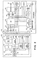
- Fig. 1 is a block diagram illustrating a configuration of an image sensing apparatus according to a first embodiment of the present invention;
- Fig. 2 is a block diagram illustrating a configuration of an image sensing apparatus according to a first modified example of the first embodiment;
- Fig. 3 is a flowchart showing a process of an operation of the image sensing apparatus according to the first modified example of the first embodiment;
- Fig. 4 is a block diagram illustrating a configuration of an image sensing apparatus according to a second modified example of the first embodiment;
- Fig. 5 is a block diagram illustrating a configuration of an image sensing apparatus according to a second embodiment of the present invention;
- Fig. 6 is a flowchart showing an operation of the image sensing apparatus according to the second embodiment;
- Fig. 7 is a flowchart showing a process of an operation of an image sensing apparatus according to a first modified example of the second embodiment;
- Fig. 8 is a flowchart showing a process of an operation of an image sensing apparatus according to a second modified example of the second embodiment;
- Fig. 9 is a flowchart showing a process of an operation of an image sensing apparatus according to a third modified example of the second embodiment;
- Fig. 10 is a flowchart showing a process of an operation of an image sensing apparatus according to a fourth modified example of the second embodiment;
- Fig. 11 shows examples of graphs of cam loci;
- Figs. 12A and 12B are block diagrams illustrating a configuration of a tiltable pan head video camera system according to a third embodiment of the present invention;
- Fig. 13 is a view of a tiltable pan head seen from a side;
- Fig. 14 is a graph of output shape of a video signal;
- Fig. 15 illustrates a configuration of an encoder;
- Fig. 16 is a graph showing the spectrum of a FSK signal;
- Fig. 17 is a block diagram illustrating a configuration of a phase synchronizing circuit; and
- Fig. 18 is a block diagram illustrating a configuration of a conventional image sensing apparatus.
-
- Preferred embodiment of the present invention will be described in detail in accordance with the accompanying drawings.
- Fig. 1 is a block diagram illustrating a configuration of an image sensing apparatus according to a first embodiment of the present invention. In Fig. 1,
reference numeral 100 denotes an image sensing unit andreference numeral 101 denotes a lens which can control functions, such as automatic focusing and zooming, by amotor driver 106, for optically forming an image of an object.Reference numeral 102 denotes a shutter, andreference numeral 107 denotes driving circuit for driving an iris (shutter). Themotor driver 106 and the drivingcircuit 107 are controlled by animage sensing controller 110. - Further,
reference numeral 103 denotes a CCD sensor as image sensing means, and the image of the object coming through thelens 101 focuses on the photo sensors of theCCD 103; and 104, a pre-processor which applies sample and hold process and automatic gain control (AGC) to an image signal read from theCCD 103, and output from the pre-processor is sent to asignal processing board 140 connected via aconnector 111 through a cable SL. - Furthermore, a
timing signal generator 108 generates a timing signal for driving theCCD 103 and thesignal processing board 140, and it also generates various kinds of timing signals on the basis of HD (horizontal synchronizing signal) and VD (vertical synchronizing signal) provided from thesignal processing board 140 through theconnector 111, and the part of the generated signals is sent to thesignal processing board 140 via theconnector 111. - A DC-
DC converter 109 provides electricity of a stable voltage for driving theCCD 103 by using a power supply provided from the signal processing board via theconnector 111. Theimage sensing controller 110 interchanges serial data with thesignal processing board 140 via theconnector 111 and controls the entireimage sensing unit 100, more specifically, zooming, iris (shutter speed) and the like, in accordance with the control data from thesignal processing board 140. - The
connector 111 is connected to aconnector 150 in thesignal processing board 140 via cable SL, and an image signal, various timing signals, signals for serial communication, power supply and signal ground, and so on, are transmitted through these connectors. It should be noted that, instead of using the cable SL, wire-less communication can be employed between theconnector 111 and theconnector 150. - The
signal processing board 140 is provided as a built-in expansion board of a computer. The image signal provided to thesignal processing board 140 via theconnector 150 is converted into a digital signal by an A/D converter 151, then the converted signal is inputted into asignal processing circuit 152. Thesignal processing circuit 152 generates a luminance signal Y and color difference signals from the image signal obtained in accordance with the color filters attached to theCCD 103. - In order to generate color difference signals, a color separation unit performs a synchronized detection and a matrix operation on the image signal in order to separate the image signal into R, G, and B signals. After that white balancing and γ correction are applied to these R, G, and B signals, then color difference signals of R-Y and B-Y and generated by using a color difference matrix. Time division duplex is performed on the color difference signals. The luminance signal Y and the duplexed color difference signals generated by the
signal processing circuit 152 are then converted into analog signals by a D/A converter 154. A synchronizing signal is added to the luminance signal by a synchronizing signal adding circuit (not shown). This luminance signal and the color difference signals are outputted to an outside of the signal processing board, from a terminal 162 and a terminal 163, respectively. Both signals can be also stored in amemory 156 in accordance with control by amemory controller 157. - The image data (a luminance signal Y and color difference signals) which is stored in the
memory 156 and the image data outputted from thesignal processing circuit 152 are transmitted to anencoder 160 alternatively by a change-over ofswitches image sensing unit 100 and an image stored in thememory 156. - Further,
reference numeral 155 denotes a bus line of a computer, which generally consists of address lines, data lines, an interruption line, lines for clock, a read signal, and a write signal, power supply, and signal ground. The signal processing board of the present invention is connected to a computer via thebus 155. - A
bus controller 153 interprets data on the data line of thebus 155 when the image sensing apparatus of the present invention is selected by an external computer, which can be determined by decoding address signals on thebus 155. By controlling thesignal processing circuit 152 and thememory controller 157 in accordance with the value of the data on the data line, and exchanging serial data with theimage sensing unit 100 via theconnector 150, theimage sensing unit 100 can be controlled. - Next, the operation of the image sensing apparatus according to the first embodiment will be described in detail. In the first embodiment, an accesses to a specific address of an address space which is accessible by a computer in accordance with an application program loaded in the computer, enables a CPU of the computer to interchange commands and data with the image sensing apparatus of the present invention. It should be noted that the specific address can be changed by a DIP type switch (not shown).
- Assuming that the specific address is assigned to an address of 2000H (H indicates a hexa-decimal number), a computer writes a command at 2000H in accordance with the program loaded in the computer, and the
bus controller 153 can determine, by decoding the address signals that the image sensing apparatus of the present invention is selected. Then thebus controller 153 receives the command via the data line and interpret it. Thebus controller 153 controls thesignal processing circuit 152 and thememory controller 157, controls various functions of theimage sensing unit 100, and reads out various status information relating to the image sensing apparatus. - For example, if the command orders to store the image signals in the
memory 156, thebus controller 153 controls thememory controller 157 to store a frame of image signals in thememory 156, and if the command orders to read the image signals from thememory 156, then thebus controller 153 sets the memory address of thememory controller 157 to an initial address of the memory which stores the image signals. After that, by incrementing the memory address thebus controller 153 outputs image data stored in thememory 156 to the data line of thebus 155. - The image sensing apparatus is configured so that no image data is outputted to the bus when the address of the address lines is not 2000H, this configuration does not have any effect on the operation of the main CPU. Further, it is possible to write data from the main CPU to the
memory 156. - If the command is related to a control of image sensing unit, such as command for zooming and focusing, the
bus controller 153 sends the command to theimage sensing unit 100 via theconnector 150 through the serial communication line. Theimage sensing controller 110 performs the operation in accordance with the command, so that theimage sensing unit 100 is controlled. - As described above, by performing command writing and data reading at the specific address in accordance with an application program loaded in the computer, the main CPU can control the image sensing apparatus. In that case, what is written by using the application program loaded in the computer includes not only the command but also parameters which are necessary to perform various controls.
- Further, when a single command is executed by the
bus controller 153 of the image sensing apparatus of the present invention, a response status data corresponding to the command is set in the status register of thebus controller 153, then the status data is transmitted to the data line of thebus 155 when the next reading operation of the specific address is performed. Thereby, the status data is returned to the main CPU, and the operational situation of the image sensing apparatus can be transmitted. - Further, when there is a command related to a request to read out the status data, functions, or the like, the information is set in the status register in the
bus controller 153 after the status data corresponding to the command is set, this makes it possible that unnecessary data need not be read out. - Referring to Fig. 2, a configuration and operation of an image sensing apparatus according to a first modification of the first embodiment will be described. Fig. 2 is a block diagram illustrating the configuration of the image sensing apparatus according to the first modification of the first embodiment. In Fig. 2, the same reference numerals as in Fig. 1 denotes the same elements, devices, or the like. In the first modification, the
signal processing circuit 152 which is constructed in hardware in the first embodiment is replaced by a DSP (Digital Signal Processor) 201 which can load an application program. TheDSP 201 can perform programmable signal processing, not fixed signal processing, by a program loaded from the main CPU through thecomputer bus 155 via thebus controller 153. Since theimage sensing unit 100 and thesignal processing board 140 are electrically connected, the bus controller of thesignal processing board 140 can detect the change when theimage sensing unit 100 is changed to another unit. - An operation to change a signal processing at the
DSP 201 when theimage sensing unit 100 is changed to another unit, is described below referring to a flowchart of Fig. 3. - First, when a fact that the
image sensing unit 100 is newly connected is detected by thebus controller 153, process starts at step S301. At S302, thebus controller 153 transmits a read request command for reading out CCD information to theimage sensing controller 110 of theimage sensing unit 100 through a serial communication line. The CCD information includes information as to the number of pixels in the CCD contained in theimage sensing unit 100, color filter information, information indicating which, NTSC or PAL, method is selected, and the like. Upon reception of the command, theimage sensing controller 110 which has a memory for storing these information in advance immediately sends back the CCD information to thebus controller 153 through the serial communication line. - The
bus controller 153 waits to receive the CCD information at step S303, and after receiving the CCD information, the controller analyzes the CCD information at step S304, then outputs a request to the main CPU to load a signal processing program. This program is suitable forCCD 103 of theimage sensing unit 100 which is connected to thesignal processing board 140 at present (S305). This process is performed by interrupting operation of the main CPU by thebus controller 153 through the interruption line of thebus 155. - Practical load-down of program, program data is written by the main CPU, from time to time at addresses assigned to the image sensing apparatus of the first modification, thereby the
bus controller 153 receives program data through the data bus of thebus 155, and transfers the data to a program memory area of theDSP 201 in order to store the data. - When the program is loaded, (YES, at step S306), then the process proceeds to step S307, where the
bus controller 153 controls theDSP 201 to execute the loaded program. Thereby, process of the image signal sent from theimage sensing unit 100 is started, and it becomes possible to store a video signal in thememory 156 and to output the video signal through an external output terminal. Further, when thesignal processing board 140 and theimage sensing unit 100 are electrically disconnected (which indicates that theimage sensing unit 100 is disconnected from the board 140), operation of theDSP 201 is stopped. In order to restart theDSP 201, the aforesaid process is necessary. - In the first modification, the
bus controller 153 detects a connection between thesignal processing board 140 and theimage sensing unit 100, and,performs a loading of an application program, however, it is possible to make the main CPU perform these operations. In that case, the operation of the main CPU should be interrupted when theimage sensing unit 100 is connected of theboard 140, so that the main CPU can start reading CCD information and loading the program. - Fig 4 is a block diagram of an image sensing apparatus according to a second modification of the first embodiment, where the apparatus has the
image sensing controller 110, which is located in theimage sensing unit 100 in the first modification, in thesignal processing board 140. The image sensing apparatus according to the second modification is able to directly control from the signal processing board, themotor driver 106 and the drivingcircuit 107 of theimage sensing unit 100. In the image sensing apparatus according to the second modification, a plurality of terminal pins (not shown) for discrimination of CCD information are so provided between theconnectors image sensing unit 100 in accordance with the CCD information. This configuration enables thesignal processing board 140 to discriminate the CCD information according to the ON/OFF information represented by the terminal,pins, thus the program to be loaded in theDSP 201 can be selected. - Note that the
image sensing unit 100 may contain a ROM for storing the CCD information so that the CCD information can be read out from the ROM. - According to the first embodiment and its modifications, the signal processing circuit can be image input means of a notebook type personal computer, or the like, if the signal processing circuit is provided on a PCMCIA (Personal Computer Memory Card International Association) card.
- Accordingly, by providing the signal processing circuit on the PCMCIA card, it is possible for an apparatus such as a notebook type personal computer, which cannot attach a video capture board, or the like to obtain image input means easily and at low price.
- As described above, by making it possible for the computer to control operations such as zooming operation and focusing, which are conventionally performed by a video camera, the image sensing apparatus according to the aforesaid first embodiment can reproduce a high resolution image signal with less deterioration by employing an inexpensive structure, and its various image sensing elements can be controlled by a computer easily. These effects can be obtained, as described above, by separating an image sensing unit from a signal processor, directly inputting an image signal from the CCD, which is obtained at the image sensing unit, into an expansion board contained in the computer, performing various signal processings in the expansion board of the computer for producing Y, R-Y, and B-Y signals, and communicating between the image sensing unit and the expansion board of the computer.
- Further, the image sensing apparatus according to the aforesaid first embodiment is able to response to changes of arrangement of the color filters and changes of the number of pixels of a CCD in the image sensing unit, by changing the application program loaded in a DSP without changing the hardware of the signal processor. This is because signal processing conventionally performed by the expansion board contained in the computer have been changed to be performed by a DSP on which the program can be loaded.
- A second embodiment of the present invention will be described below in detail.
- Fig. 5 is a block diagram illustrating a brief configuration of an image sensing apparatus according to the second embodiment of the present invention. In Fig. 5, the same reference numerals as in Fig. 1 denotes the same elements, devices, or the like. In Fig. 5,
reference numeral 100 denotes an image sensing unit; 101-2, a fixed first group of lenses; 102-2, a zoom lens; 103-2, an iris diaphragm; 104-2, a fixed third group of lenses; and 105-2, a focusing lens having functions of correcting the movement of a focusing point in accordance with zooming and of focusing. Further, reference numeral 111-2 denotes a stepping motor; 108-2, a motor driver for driving the stepping motor 111-2; 113-2, a stepping motor for moving the focusing lens 105-2; 110-2, and a motor driver for driving the stepping motor 113-2. - Further, reference numeral 112-2 denotes an ig meter for controlling opening of the iris diaphragm 103-2; 109-2, a driving circuit for driving the ig meter 112-2; 118-2, a zoom encoder for detecting position information of the zoom lens 102-2; 119-2, an iris encoder for detecting a value of iris opening; and 120-2, a focus encoder for detecting position information of the focusing lens 105-2. The
image sensing controller 110 finds the position information of the zoom lens and the focusing lens by using the zoom encoder 118-2 and the focus encoder 120-2, and drives the stepping motors 111-2 and 113-2 by controlling the motor drivers 108-2 and 110-2 in order to perform automatic focusing and a zooming operation on the basis of the position information, thus moving the zoom lens 102-2 and the focusing lens 105-2. Furthermore,reference numeral 103 denotes a CCD as image sensing means, and an image of an object is focused on a photo sensing surface of theCCD 103 by aforesaid groups of lenses. - Further,
reference numeral 153 denotes a bus controller which controls communication between thebus 155 and asignal processing controller 164. Thesignal processing controller 164 communicates with all components on thesignal processing board 140 and thebus 155, and exchanges serial data with theimage sensing unit 100 through theconnector 150, thereby controls theimage sensing unit 100. - Next, an operation of the image sensing apparatus according to the second embodiment will be described referring to a flowchart of Fig. 6.
- First, when power is turned on or when the
image sensing unit 100 is detected as being it is newly connected, asignal processing controller 164 in Fig. 5 sends a request command for reading a cam locus table to theimage sensing controller 110 in order to load the cam locus table, which contains cam locus data inherent to the groups of lenses of the image sensing unit, into a memory of thesignal processing controller 164 at step S201. Theimage sensing controller 110 has a memory for storing these data, and when the controller receives the aforesaid request command, it sends the cam locus table to thesignal processing controller 164 by using serial communication. Thesignal processing unit 164 reads the entire data in the cam locus table and stores it in a memory of thesignal processing unit 164 at step S202. - As described above, when the cam locus table is completely loaded, the controller sends a request for initializing the
image sensing unit 100, then theimage sensing unit 100 is operated at step S203. Accordingly, processing of an image signal sent from theimage sensing unit 100 is started. - After the aforesaid process, when the application program in the computer is executed to send a command for zooming to the
signal processing controller 164 via thecomputer bus 155, thesignal processing unit 164 extracts the distinction of the image of the object on the display from the image signal sent from theimage sensing unit 100 to thesignal processing circuit 152. Then, thesignal processing unit 164 sends operational information of the groups of lenses to theimage sensing controller 110, the information is determined by the distinction of the image and the cam locus table loaded in the memory of thesignal processing controller 164. Thesignal controller 110 controls the operations of the zoom lens 102-2 and the focusing lens 105-2 in accordance with the operational information. - As described above, it is possible to control various kinds of image sensing units haying different cam loci to perform the most suitable focusing and zooming operation.
- Further, in the image sensing apparatus according to the second embodiment, similarly to the first embodiment, when the
signal processing board 140 and theimage sensing unit 100 are electrically disconnected (when the image sensing unit is disconnected), thesignal processing controller 164 stops signal processing in the signal processing board, and in order to restart, the processing the same process as described above is followed. - A modification of the aforesaid second embodiment will be described below. The configuration of the image sensing apparatus according to the first modification is the same as in the second embodiment, thus the explanation of elements, devices, or the like, is omitted.
- Fig. 7 is a flowchart showing an operation of the image sensing apparatus according to the first modification of the second embodiment.
- In the first modification, when power is turned on, or when the
image sensing unit 100 is detected as being newly connected, thesignal processing controller 164 sends a request command for reading the cam locus table to theimage sensing controller 110 in order to load such parameters as the cam locus table which contains cam locus data inherent to the groups of lenses of theimage sensing unit 100, speed information such as fastest operation speed of the zoom lens and the focusing lens, distance between the wide end to the tele-end of the zoom lens and its step amount, and distance between the closest and the farthest focal length and step amount of the focusing lens, to a memory of thesignal processing controller 164 at step S301-1. - The
image sensing controller 110 has a memory for storing these data in advance, and when theimage sensing controller 110 receives the aforesaid command, it transmits these data to thesignal processing controller 164 by using serial communication. Then, thesignal processing controller 164 stores the entire data in its memory at step S302-1. - Next, the
signal processing controller 164 issues a transmission request command against the main CPU of a computer in order to send these data to the CPU through thebus 155 at step S303-1. Then thesignal processing controller 164 waits until the main CPU is ready for receiving the data at step S304-1. When the main CPU is ready to receive data, thesignal processing controller 164 starts sending the data at step S305-1. - After sending all the data to the main CPU, the
signal processing controller 164 drives theimage sensing unit 100 at step S306-1, and starts processing an image signal sent from theimage sensing unit 100. The subsequent operation is the same as that in the second embodiment, thus the explanation of it is omitted. - In the first modification of the second embodiment as described above, it is possible for the
image sensing unit 100 having different cam loci to perform the most suitable focusing and zooming operations. After same time, the computer can perform most suitable control of theimage sensing unit 100 in accordance with an application program, since the computer is aware of the control parameters of the groups of lenses of theimage sensing unit 100 with the aid of the data sent from thesignal processing controller 164. - It should be noted that, after the
signal processing board 140 and theimage sensing unit 100 are electrically disconnected (when the image sensing unit is disconnected), the same process as in the second embodiment is followed. - Fig. 8 is a flowchart showing an operation of an image sensing apparatus according to the second modification of the second embodiment.
- In the second modification, when power is turned on, or when the
image sensing unit 100 is detected as being newly connected, thesignal processing controller 164 sends an ID request command to theimage sensing controller 110, in order to read the ID possessed by theimage sensing unit 100, at step S401. Theimage sensing controller 110 has a built-in memory for storing the ID, and when the controller receives the aforesaid command, it sends the ID to thesignal processing controller 164 by using serial communication. - The
signal processing controller 164 waits until theimage sensing controller 110 finishes reading the ID at step S402, and when theimage sensing controller 110 has finished it, the controller sends a request command for sending the data to the main CPU of a computer, in order to load such parameters relating to zooming and focusing as the cam locus table, speed information such as fastest operation speed of the zoom lens and the focusing lens, distance between the wide-end and the tele-end of the zoom lens and its step amount, and distance between the closest and the farthest focal length and step amount of the focusing lens, all of which are suitable to the ID, to a memory of thesignal processing controller 164 at step S403. - The computer stores these the data in a storage medium, such as a hard disc and a floppy disk (not shown), and selects the data corresponding to the ID, then sends it to the
signal processing controller 164. Thesignal processing controller 164 reads the entire data sent from the main CPU, and stores it in the memory of thesignal processing controller 164 at step S404. When thesignal processing controller 164 has finished loading all the data from the main CPU, the controller transmits a request for initializing theimage sensing unit 100, instructs the image sensing unit to work at step S405, and starts processing image signals sent by theimage sensing unit 100. - The subsequent operation is the same as that in the second embodiment, thus the explanation of it is omitted.
- According to the second modification of the second embodiment as described above, since the data, such as cam loci suitable for the groups of lenses in the
image sensing unit 100, is provided from the main CPU, the data as parameters can be freely changed by an application program of the computer. - Further, in the image sensing apparatus according to the second modification, similarly to the first embodiment, when the
signal processing board 140 and theimage sensing unit 100 are electrically disconnected (when the image sensing unit is disconnected), thesignal processing controller 164 stops signal processing in the signal processing board, and in order to restart the processing, the same process as described above is followed. - Fig. 9 is a flowchart showing an operation of an image sensing apparatus according to a third modification of the second embodiment.
- In the third modification, when power is turned on, or when the
image sensing unit 100 is detected as being it is newly connected, thesignal processing controller 164 sends an ID request command to theimage sensing controller 110, in order to read the ID possessed by theimage sensing unit 100, at step S501. Theimage sensing controller 110 has a built-in memory for storing the ID, and when the controller receives the aforesaid command, it sends the ID to thesignal processing controller 164 by using serial communication. - The
signal processing controller 164 waits until theimage sensing controller 110 finishes reading the ID at step S502, and when theimage sensing controller 110 has finished it, the controller sends a request command for sending the data to the main CPU of a computer, in order to load such parameters relating to zooming and focusing as the cam locus table, speed information, such as fastest operation speed of the zoom lens and the focusing lens, distance between the wide-end and the tele-end of the zoom lens and its step amount, and distance between the closest and the farthest focal length and step amount of the focusing lens, all of which is most suitable to the ID, to a memory of thesignal processing controller 164 at step S503. - The computer stores these data in a storage medium, such as a hard disc and a floppy disk (not shown), and selects the data corresponding to the ID, then sends it to the
signal processing controller 164 at step S504. Thesignal processing controller 164 sends the data received from the main CPU to theimage sensing controller 110 at step S505. Note that theimage sensing controller 110 has a memory for storing the data. - The
signal processing controller 164 repeats the processes of steps S504 and S505 until all the data from the main CPU is loaded. When all the data from the main CPU is loaded (YES, at step S506), thesignal processing controller 164 issues a request for initializing theimage sensing unit 100, puts theimage sensing unit 100 to work at step S507, and starts processing image signals sent by theimage sensing unit 100. - After this, when a zoom request command is sent to the
signal processing controller 164 via thebus 155 in accordance with the application program of the computer, thesignal processing controller 164 sends the zoom request command to theimage sensing controller 110, as well as extracts distinction of the image of the object from the image signal which is sent from theimage sensing unit 110 to thesignal processing circuit 152, and sends result of the extraction to theimage sensing controller 110. - The
image sensing controller 110 controls operations of the zoom lens 102-2 and the focusing lens 105-2 in accordance with calculation based on the data and the cam locus table loaded in the memory. - According to the third modification of the second embodiment as described above, since data such as cam loci suitable for the groups of lenses in the
image sensing unit 100, is provided from the main CPU, the data as parameters can be freely changed by an application program of the computer . - Further, in the image sensing apparatus according to the third modification, an operation when the
signal processing board 140 and theimage sensing unit 100 are electrically disconnected (when theimage sensing unit 100 is disconnected) is similar to that of the first embodiment. - Fig. 10 is a flowchart showing an operation of an image sensing apparatus according to a fourth modification of the second embodiment.
- In the fourth modification, when power is turned on, or when the
image sensing unit 100 is detected as being newly connected, thesignal processing controller 164 sends an ID request command to theimage sensing controller 110, in order to read the ID possessed by theimage sensing unit 100 at step S601. Theimage sensing controller 110 has a built-in memory for storing the ID, and when the controller receives the aforesaid command, it sends the ID to thesignal processing controller 164 by using serial communication. - The
signal processing controller 164 waits until theimage sensing controller 110 finishes reading the ID at step S602, and when theimage sensing controller 110 has finished it, the controller sends a request command for sending the data to the main CPU of a computer, in order to load such parameters relating to zooming and focusing as the cam locus table, speed information such as fastest operation speed of the zoom lens and the focusing lens, distance between the wide-end and the tele-end of the zoom lens and its step amount, and distance between the closest and the farthest focal length and step amount of the focusing lens all of which are suitable to the ID, to a memory of thesignal processing controller 164 at step S603. - The computer stores these data in a storage medium, such as a hard disc and a floppy disk (not shown), and selects the data corresponding to the ID, then sends it to the
signal processing controller 164, Thesignal processing controller 164 has a built-in memory for storing the data. - When all the data is loaded (YES, at step S604), the
signal processing controller 164 sends a request command for receiving data to theimage sensing controller 110 in order to send the received data to theimage sensing controller 110 at step S605. Theimage sensing controller 110 also has a built-in memory for storing these data. - When the
image sensing controller 110 received the aforesaid command, it waits until thesignal processing controller 164 sends data. When thesignal processing controller 164 sends all the received data to the image sensing controller 110 (YES, at step S606), it issues a request for initializing theimage sensing unit 100, puts theimage sensing unit 100 to work at step S607, and starts processing an image signal sent from theimage sensing unit 110. - It should be noted that the aforesaid series of operations in the fourth modification correspond to a case in which deterioration of computer performance is prevented by reducing the occupied time period of the
computer bus 155 when large amount of data is exchanged in the third modification. - Further the subsequent operation is the same as that in the third modification, thus the explanation of it is omitted.
- In the fourth embodiment as described above, since the computer knows the control parameters of the groups of lenses of the
image sensing unit 100. It is possible for the computer to perform control which is most suitable to theimage sensing unit 100, by using the application program of the computer. It is also possible for the computer to freely change these parameters by using an application program of the computer, since data such as cam loci suitable for the groups of lenses in theimage sensing unit 100 is provided by the main CPU. - Further, in the image sensing apparatus according to the fourth modification, an operation when the
signal processing board 140 and theimage sensing unit 100 are electrically reconnected (when theimage sensing unit 100 is reconnected) is similar to that of the first embodiment. It should be noted that the apparatus according to the second embodiment may store in a memory such parameters as sensitive information of image sensing devices in a camera unit, data relating to a kind of color filter, its spectrum characteristics and its array, the number of picture elements that the image sensing devices have, the number of the image sensing devices, again, characteristics of non-linearity, operational characteristics of an iris, shutter and other optical elements, and then transmit these parameters to a signal processing unit. This configuration optimizes characteristics of a signal processing and its control. - As described above, it is possible to perform the most suitable control for the exchangeable camera head unit by generating control information for the lenses dependent upon the data from a camera head unit.
- Further, by connecting a computer to an image signal processing unit, which is separated from the camera head unit, it is possible to control the camera head unit easily from the computer.
- A third embodiment of the present invention will be described below.
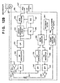
- Figs. 12A and 12B is a block diagram of the electrical configuration of a tiltable pan head video camera system according to the third embodiment of the present invention. In Fig. 12A,
reference numeral 348 denotes a video camera head; 349, a modulation/demodulation circuit block on a rotatable stage of a pan head; and in Fig. 12B,reference numeral 350 denotes a modulation/ demodulation circuit block on a base. Further,reference numeral 301 denotes an image sensor, e.g., a CCD; 302, a sample/hold and AGC circuit; 303, an encoder for converting a signal to a signal with a predetermined format; 304, driver for theimage sensor 301; 305, a timing signal generator for generating various kinds of timing pulses necessary for driving theimage sensor 301; 306, a synchronizing signal generator (SSG); and 307, a microcomputer. - Further,
reference numeral 308 denotes external input/output terminals of the video camera head; 309, a connecting cable; 310, connecting terminals of a video camera in a rotatable stage of the pan head; 311, an AM modulator; 312, a band pass filter (BPF); 313, a microcomputer; 314, an FSK modulator; 315, a band pass filter (BPF); 316, an adder; 317, an FSK demodulator; 318, a band pass filter (BPF); and 319 and 320, buffer amplifiers. - Further,
reference numeral 321 denotes tilt driving motor; 322, a DC-DC converter; 323, a low pass filter (LPF); 324, a capacitor for impending a DC current; 325, an output matching resistor; 326, a pan shaft which . forms an external conductor of a signal-color type coaxial construction; and 327, a core cable forming a central conductor of the signal-core type coaxial. construction. -
Reference numeral 328 denotes an inductor; 329 and 330, buffer amplifiers; 331, a band pass filter; 332, an AM demodulator; 333, a low pass filter (LPF); 334, a sensor processing circuit; 335, an NTSC encoder; 336, a phase-locked loop' circuit (PLL); and 337, a synchronizing signal generator (SSG). - Further,
reference numeral 338 denotes a microcomputer; 339, an FSK demodulator; 340, a band pass filter (BPF); 341, an output matching resistor; 342, an FSK modulator; 343, a band pass filter; 344, a pan driving motor; 345, a power supplying circuit; 346, an AC plug; and 347, external input/output terminals on the base. - Fig. 13 illustrates side view showing a configuration of a tiltable pan head according to the third embodiment. It should be noted that elements, devices, or the like, which are not directly related to the present invention are not shown in the figure.
- In Fig. 13,
reference numeral 361 denotes an object lens; 362, a tilt rotational shaft; 362a, a tilt shaft holder; 363, a tilt base; 364, a pan head; 365, a pan shaft holder; 366, a base; and 367 and 368, connecting cables. Note that, in Fig. 13, the same reference numerals as in Fig. 12 denote the same elements, devices or the like, and the explanation of them are omitted. - Next, an operation according to the third embodiment will be explained with reference to Figs. 12 and 13.
- When an AC power is supplied to the
power supplying circuit 345 via the AC plug 346 of the modulation/demodulation circuit block 350 on thebase 366, a predetermined DC voltage is applied to theentire circuit block 350, as well as to thecore cable 327 of thepan head 326 via theinductor 328. The DC voltage is also applied to thecircuit block 349 of thepan head 364 via thecore cable 327, where noises on the DC current are eliminated by passing the current through thelow pass filter 323. The DC voltage is then converted to a desired DC voltage by the DC-DC converter 322. - The DC voltage puts electrical circuits of the
circuit block 349 to work and is applied to connecting terminals of thevideo camera 310 and further provided to thevideo camera head 348 via the connectingcable 309, thus turning on thevideo camera 348. Themicrocomputer 307 of thevideo camera 348 performs predetermined initialization after the power is turned on, thereby the video camera starts functioning. - An image focused by the
object lens 361 in Fig. 13 induces prescribed amount of electrical charge on each pixel of theimage sensor 301 which consists of, e. g., a CCD, and the electrical charge on each pixel is detected by thesensor 301 as a voltage information. The voltage information is processed by a sample and hold method at the sample/hold andAGC circuit 302, in accordance with a predetermined sampling signal, thereby a desired image information is extracted. - Immediately after, a signal having the extracted information passes through an automatic gain control amplifier (AGC) where the signal is adjusted to have a predetermined amplitude level, then the signal is sent to the
encoder 303. After processed at the AGC, theencoder 303 encodes the image information (referred as "video information", hereinafter) into a signal having a format of video signal output as shown in Fig. 14. - In Fig. 14,
reference numeral 371 denotes a horizontal synchronizing signal equivalent to a signal in the NTSC method, lasting about 5 µsec; 372, an area for a color burst signal which can contain about 8 to 12 cycles of color sub-carrier signals of 3.58 MHz in the NTSC method, however, in the third embodiment instead of these sub-carrier signals, a pixel clock lasting 2.4 µsec for horizontal reading of thesensor 301 is inserted. It should be noted that a vertical synchronizing signal and an equalizing pulse are the same as those in the NTSC method. - Fig. 15 is a diagram illustrating the configuration of the
encoder 303, in Fig. 15,reference numeral 381 denotes a buffer amplifier; 382, an adder; and 387, a video amplifier. Inputted video information is sent to theadder 382 after passing through thebuffer amplifier 381. Whereas, regarding acomposite synchronizing signal 383 generated by the synchronizing signal generator, a pixel clock 384 (if a CCD sensor has 405 pixels, it is 4 fsc, where 2.12 fsc is 3.58 MHz of the color sub-carrier signal), and a color burst flag (CBF) 385, thecomposite synchronizing signal 383 is directly sent to theadder 392, while the pixel clock is selected during a period determined by the color burst flag (CBF) 385 at agate circuit 386, and the selected clock is sent to theadder 382. - Thereby a video signal shown in Fig. 14, is obtained as an output signal from the
adder 382, and that signal is outputted through thevideo amplifier 387. - The video signal having the form shown in Fig. 14 at the
encoder 303 is sent to the modulate/demodulate circuit block 349 on thepan head 364, via the external input/output terminals 308 and the connectingcable 309. In thecircuit block 349, the video signal is amplitude modulated of a carrier signal of, e.g., 70 MHz as shown in Fig. 16, which shows characteristics of a frequency arrangement of the amplitude modulation. The reason for using a high frequency of carrier signal, namely 70 MHz, is as follows, by off-setting the signal level effected by an arrangement of on-chip color filter on the sensor, it is necessary to expect a bandwidth of ten times as wide as the ordinary video signal of 5.5 MHz (band width for 4 mega pixels), namely 55 MHz. - It should be noted that Fig. 16 contains the spectrum of an FSK signal, however, the signal is used for controlling the
tilt driving motor 321 and thevideo camera 348, which is not directly related to the present invention, thus the explanation of it is omitted. - After removing noises in the video signal out of desired band width by the
band pass filter 312, the amplitude modulated video signal is sent to theadder 316. Theadder 316 superposes the FSK modulated signal (300KHz/310KHz, for instance) on the above-mentioned video signal and the resultant duplexed signal is outputted to thecore cable 327 of panshaft of the signal-core type coaxial construction through thebuffer amplifier 320 and theoutput matching resistor 325. - The duplexed signal reaches the
band pass filter 331 via thebuffer amplifier 329, in which only amplitude modulated component is separated from the duplexed signal. After that, theAM demodulator 332 demodulate the AM component, then useless high frequency component in the AM component is removed by thelow pass filter 333, thereby obtaining the video signal of the type shown in Fig. 14. - The video signal is sent to the
sensor processing circuit 334 and the phase-lockedloop circuit 336. Thecircuit 336 reproduces a continuous pixel clock synchronized with the pixel clock 372 (shown in Fig. 14) having a burst state. The continuous pixel clock is provided to thesensor processing circuit 334 as well as to the synchronizingsignal generator 337 where the various kinds of desired synchronizing signals are generated based on the transmitted continuous pixel clock. - In the
sensor processing circuit 334, plural kinds of processes, such as decoding of color filtered signal from of a sensor, γ-process, matrix process, are performed in accordance with the video signal and the continuous pixel clock, then the processed signal is outputted to theNTSC encoder 335 in a form of, for instance, a luminance signal and color difference signal. - The output from the NTSC encoder is transmitted to a codec of a teleconference system, for example, as a final video output of the video camera.
- The operation of the aforesaid phase-locked
loop circuit 336 will be described supplementary. Fig. 17 is a detailed block diagram of the phase-locked loop circuit as one example. In Fig. 17,reference numeral 390 denotes a gate circuit capable of controlling passage of a signal in accordance with a control signal; 391, a phase comparator (PD); 392, a filter for phase compensation of a control signal in a phase-locked loop; 393, a voltage controlled oscillator having the pixel clock as a central frequency; 394, a separating circuit of a synchronizing signal, especially, a horizontal synchronizing signal; 395, a pulse delay circuit by mono-stable multivibrator; 396, a mono-stable multivibrator (MM) generating a pulse with a predetermined pulse width. - The video signal having the wave shape in Fig. 14 is transmitted to the
gate circuit 390 and the synchronizingsignal separating circuit 394, and in the latter circuit, a horizontal synchronizing signal is separated. The horizontal synchronizing signal is converted to a burst flag pulse by thepulse delay circuit 395 and the mono-stable multivibrator 396. Then the burst flag pulse is sent to thegate circuit 390. Thegate circuit 390 is "ON" only while the burst flag pulse is sent, and selectively outputs a burst shaped pixel clock. - The burst-shaped pixel clock is sent to the
phase comparator 391 as a standard signal, in which the clock is compared with the continuous clock from the voltage controlled oscillator in terms of phase. An erroneous output from thephase comparator 391, after being phase compensated by the loop filter, controls thevoltage control oscillator 393 so that the erroneous output disappears. Accordingly, a continuous pixel clock which is synchronized with the burst-type pixel clock is obtained. - As described above, tiltable pan head video camera system of this type, a video camera head of reduced size and weight with no processing circuit is realized by outputting an unprocessed video signal from a sensor, superposed with the burst pixel clock and a composite synchronizing signal, and by providing the processing circuit on the base.
- Further, since video camera head is light in weight, the rotational speed of the tiltable pan head becomes higher.
- In an image sensing apparatus, by forming a signal processing unit which processes a signal from an image sensing unit on an expansion board of a computer or a PCMCIA card, it is possible to easily control the image sensing unit, process a signal from the computer, and by taking an image signal into an image processing unit immediately, reduces deterioration of the signal. Further, the image sensing unit is separated from the signal processing unit, and data specific to the image sensing unit is processed by the signal processing unit, thereby various types of image sensing units can be controlled.
Claims (22)
- An image sensing apparatus consisting of a camera head unit (100) for forming an optical image of an object and for converting the optical image into an electrical image signal, and of an image signal processing unit (140), connected to said camera head unit (100) via a communication line (111, 150, SL), for performing predetermined process on the electrical image signal sent from said camera head unit,
wherein said camera head unit (100) comprises:and wherein said image signal processing unit (140) comprises:storage means for storing characteristic data of said camera head unit; andtransmission means (111) for transmitting the characteristic data to said image signal processing unit via the communication line,wherein said image signal processing unit includes a bus interface (155) for communicating with a PC, and said camera head unit (100) controls operations of the camera head unit (100) on the basis of the command sent from said PC through said image signal processing unit (140), andgenerating means for generating control information for the camera head unit (100) based on the characteristic data transmitted from said camera head unit and the electrical image signal from said camera head unit; andtransmission means (150) for transmitting the control information to said camera head unit via the communication line (111, 150, SL),
wherein said image signal processing unit (140) and said camera head unit (100) are provided separately. - The image sensing apparatus according to claim 1,
wherein the electrical image signal is a color signal corresponding to the output of a color filter provided in front of an image sensing means (103). - The image sensing apparatus according to claim 1,
wherein the electrical image signal is composed of a luminance signal and a color difference signal. - The image sensing apparatus according to claim 1,
wherein said camera head unit (100) further comprises:image forming means (101, 102) for forming an optical image of an object;image sensing means (104) for converting the optical image formed by said image forming means (101) into an electrical image signal; andcontrol means (110) for controlling said image forming means (101, 102). - The image sensing apparatus according to claim 1,
wherein
said image signal processing unit (140) further comprises:signal processing means (201), connected with said camera head unit via said communication line, for performing predetermined process on the electrical image signal provided by said camera head unit;storage means (156) for storing the image signal obtained by said signal processing means; andcommunication means (150, 153) for exchanging predetermined data with said camera head unit (100). - The image sensing apparatus according to claim 4,
wherein said control means (110) operates on the basis of control information transmitted from said image signal processing unit (140) via said communication means (150, 153). - The image sensing apparatus according to claim 1,
wherein said image signal processing unit (140) is constructed on an expansion board which is contained in a computer. - The image sensing apparatus according to claim 7,
wherein the control information is generated by the computer. - The image sensing apparatus according to claim 7,
wherein the computer writes in or reads out an image signal to/from said storage means (165). - The image sensing apparatus according to claim 5,
wherein said predetermined process performed by said signal processing means (201) is variable. - The image sensing apparatus according to claim 10,
wherein the predetermined process is changed in accordance with a predetermined program. - The image sensing apparatus according to claim 7,
wherein said predetermined signal process performed by said signal processing means (201) is variable with the aid of an application program loaded from the computer. - The image sensing apparatus according to claim 1,
wherein the characteristic data is related to cam loci of the group of lenses (101). - The image sensing apparatus according to claim 1,
wherein the characteristic data includes parameters corresponding to an identifier of said camera head unit (100), cam loci of the group of lenses (101), and zooming and focusing of the group of lenses (101). - The image sensing apparatus according to claim 14,
wherein said image signal processing unit (140) is connected to a computer via a predetermined interface (155), the computer selects characteristic data corresponding to the identifier out of the characteristic data stored in advance, and sends the selected characteristic data to the image signal processing unit (140) via the interface. - The image sensing apparatus according to claim 15,
wherein said image signal processing unit (140) generates the control information for the group of lenses on the basis of the characteristic data sent from the computer. - The image sensing apparatus according to claim 1,
further comprising:a rotatable stage which includes a video camera having an image sensor and of a base for holding said rotatable stage, said rotatable stage and said base are connected by a rotational shaft, including:combining means in said video camera for adding and combining at least a pixel clock, a composite synchronizing signal, and image information from said image sensor before predetermined camera process, andmodulating means for modulating a siganl from said combining means. - The image sensing apparatus according to claim 17,
wherein the camera process includes at least decoding of a color filtered signal from the image sensor, γ-correction, and color conversion matrix process. - The image sensing apparatus according to claim 17,
wherein said base has processing means for performing the camera process. - The image sensing apparatus according to claim 17,
wherein the rotatable shaft has a signal-core coaxial configuration. - A camera head unit (100) for forming an optical image of an object and for converting the optical image into an electrical image signal, connected to an image signal processing unit (140) via a communication line (111, 150, SL),
wherein said image signal processing unit performs predetermined process on the electrical image signal sent from said camera head unit,
wherein said image signal processing unit comprises:wherein said image signal processing unit includes a bus interface (155) for communicating with a PC, andgenerating means for generating control information for the camera head unit (100) based on a characteristic data transmitted from said camera head unit; andtransmission means (150) for transmitting the control information to said camera head unit via the communication line (111, 150, SL),
wherein said image signal processing unit is provided separately from said camera head unit,
wherein said camera head unit comprises:wherein said camera head unit (100) controls operation of said camera head unit on the basis of the command sent from said PC through said image signal processing unit.storage means for storing said characteristic data of said camera head unit, andtransmission means (111) for transmitting the characteristic data to said image signal processing unit via the communication line, and - An image signal processing unit (140) connected to a camera head unit (100) via a communication line (111, 150, SL),
wherein said camera head unit forms an optical image of an object and for converting the optical image into an electrical image signal, and
wherein said camera head unit comprises:.wherein said image signal processing unit performs predetermined process on the electrical image signal sent from said camera head unit,storage means for storing characteristic data of said camera head unit, andtransmission means (111) for transmitting said characteristic data to said image signal processing unit via the communication line,
wherein said image signal processing unit comprises:wherein said image signal procesing unit includes a bus interface (155) for communicating with a PC, so that said camera head unit controls operation of said camera head unit on the basis of the command sent from the PC through said image signal processing unit (140), andgenerating means for generating control information for the camera head unit (100) based on the characteristic data transmitted from the camera head unit, andtransmission means (150) for transmitting the control information to said camera head unit via the communication line (111, 150, SL),
wherein said image signal processing unit is provided separately from said camera head unit.
Applications Claiming Priority (9)
| Application Number | Priority Date | Filing Date | Title |
|---|---|---|---|
| JP29505/94 | 1994-02-28 | ||
| JP02950594A JP3461194B2 (en) | 1994-02-28 | 1994-02-28 | Imaging device and data processing method |
| JP2950594 | 1994-02-28 | ||
| JP06091690A JP3129600B2 (en) | 1994-04-28 | 1994-04-28 | Pan-tilt video camera system |
| JP9169094 | 1994-04-28 | ||
| JP91690/94 | 1994-04-28 | ||
| JP24205/95 | 1995-02-13 | ||
| JP7024205A JP3046214B2 (en) | 1995-02-13 | 1995-02-13 | Imaging device |
| JP2420595 | 1995-02-13 |
Publications (2)
| Publication Number | Publication Date |
|---|---|
| EP0674435A1 EP0674435A1 (en) | 1995-09-27 |
| EP0674435B1 true EP0674435B1 (en) | 2002-11-27 |
Family
ID=27284554
Family Applications (1)
| Application Number | Title | Priority Date | Filing Date |
|---|---|---|---|
| EP95102412A Expired - Lifetime EP0674435B1 (en) | 1994-02-28 | 1995-02-21 | Image sensing apparatus |
Country Status (5)
| Country | Link |
|---|---|
| US (2) | US6046769A (en) |
| EP (1) | EP0674435B1 (en) |
| KR (1) | KR0179710B1 (en) |
| CN (1) | CN1042085C (en) |
| DE (1) | DE69528918T2 (en) |
Families Citing this family (48)
| Publication number | Priority date | Publication date | Assignee | Title |
|---|---|---|---|---|
| US6630949B1 (en) * | 1992-12-01 | 2003-10-07 | Canon Kabushiki Kaisha | Image processing system and information processing apparatus |
| US6407773B1 (en) * | 1994-02-28 | 2002-06-18 | Canon Kabushiki Kaisha | Image sensing apparatus |
| DE69528918T2 (en) | 1994-02-28 | 2003-04-24 | Canon Kk | Imaging device |
| US20020082043A1 (en) * | 1994-05-19 | 2002-06-27 | Kari-Pekka Wilska | Device for personal communications, data collection and data processing, and a circuit card |
| US6414714B1 (en) * | 1994-10-07 | 2002-07-02 | Sony Corporation | Video camera and video camera setup method |
| EP0786715A3 (en) | 1996-01-29 | 1999-06-09 | Canon Kabushiki Kaisha | Electronic apparatus |
| US6256063B1 (en) * | 1996-10-02 | 2001-07-03 | Fuji Photo Film Co., Ltd. | Image signal processing unit and electronic still camera |
| US6965400B1 (en) * | 1997-02-07 | 2005-11-15 | Canon Kabushiki Kaisha | Video input apparatus and image pickup system including the apparatus |
| US6437824B1 (en) | 1997-02-07 | 2002-08-20 | Canon Kabushiki Kaisha | Image pickup apparatus and system |
| US6563534B1 (en) * | 1997-03-27 | 2003-05-13 | Hitachi Denshi Kabushiki Kaisha | High definition television camera apparatus for correcting a characteristic value of a video signal |
| US6608647B1 (en) * | 1997-06-24 | 2003-08-19 | Cognex Corporation | Methods and apparatus for charge coupled device image acquisition with independent integration and readout |
| US6738090B2 (en) * | 1997-10-23 | 2004-05-18 | Eastman Kodak Company | System and method for using a single intelligence circuit for a plurality of imaging rendering components |
| US6597394B1 (en) * | 1997-11-16 | 2003-07-22 | Pictos Technologies, Inc. | Programmable image transform processor for digital image processing |
| US6989865B1 (en) | 1997-12-19 | 2006-01-24 | Canon Kabushiki Kaisha | Optical equipment and it control method, and computer-readable storage medium |
| FI105382B (en) * | 1998-01-23 | 2000-07-31 | Nokia Mobile Phones Ltd | Procedure for transmitting image information |
| US6822684B1 (en) | 1998-04-03 | 2004-11-23 | Canon Kabushiki Kaisha | Image signal recording system and optical device |
| JP3652125B2 (en) | 1998-07-10 | 2005-05-25 | キヤノン株式会社 | Imaging control apparatus, imaging control method, imaging control system, and storage medium |
| JP3423620B2 (en) * | 1998-07-30 | 2003-07-07 | キヤノン株式会社 | Imaging device and control device, imaging device control system, control method therefor, and storage medium |
| JP2000050129A (en) * | 1998-07-31 | 2000-02-18 | Minolta Co Ltd | Digital camera |
| WO2000050955A1 (en) * | 1999-02-22 | 2000-08-31 | Welch Allyn, Inc. | Digital camera adaptor assembly |
| US7898571B1 (en) * | 1999-02-27 | 2011-03-01 | Raytheon Company | Versatile video data acquisition and analysis system |
| US7009644B1 (en) | 1999-12-15 | 2006-03-07 | Logitech Europe S.A. | Dynamic anomalous pixel detection and correction |
| US6995794B2 (en) * | 1999-06-30 | 2006-02-07 | Logitech Europe S.A. | Video camera with major functions implemented in host software |
| EP1069756A3 (en) * | 1999-07-14 | 2004-03-10 | Eastman Kodak Company | Method of operating a multiple component electronic imaging system |
| JP4399133B2 (en) * | 2000-09-08 | 2010-01-13 | カシオ計算機株式会社 | Imaging condition providing device, imaging condition setting system, and imaging condition providing method |
| US7471310B2 (en) * | 2001-12-28 | 2008-12-30 | Karl Storz Imaging, Inc. | Intelligent camera head |
| WO2003077530A2 (en) * | 2002-03-05 | 2003-09-18 | Hitron Usa | Quick-release sensor assembly and method |
| US20030174238A1 (en) * | 2002-03-12 | 2003-09-18 | Wu Vic Chi-Shi | Hot-swappable camera head system and method |
| US7466344B2 (en) * | 2002-06-07 | 2008-12-16 | Scimeasure Analytical Systems, Inc. | High-speed low noise CCD controller |
| JP4298358B2 (en) * | 2003-04-08 | 2009-07-15 | キヤノン株式会社 | Image processing system |
| KR100601460B1 (en) * | 2003-06-23 | 2006-07-14 | 삼성전기주식회사 | Apparatus and method for interfacing between image sensor and image processor |
| JP2005197922A (en) * | 2004-01-06 | 2005-07-21 | Fuji Xerox Co Ltd | Image reading apparatus |
| US7095435B1 (en) * | 2004-07-21 | 2006-08-22 | Hartman Richard L | Programmable multifunction electronic camera |
| US7855727B2 (en) * | 2004-09-15 | 2010-12-21 | Gyrus Acmi, Inc. | Endoscopy device supporting multiple input devices |
| US7602422B2 (en) * | 2005-07-08 | 2009-10-13 | Seiko Epson Corporation | Serial camera interface |
| US7859574B1 (en) * | 2005-07-19 | 2010-12-28 | Maxim Integrated Products, Inc. | Integrated camera image signal processor and video encoder |
| US8135068B1 (en) | 2005-07-19 | 2012-03-13 | Maxim Integrated Products, Inc. | Method and/or architecture for motion estimation using integrated information from camera ISP |
| US20070040471A1 (en) * | 2005-08-17 | 2007-02-22 | Nokia Corporation | Load adaptive class de driving amplifier for piezoelectric actuators |
| US7684090B2 (en) | 2005-12-20 | 2010-03-23 | Eastman Kodak Company | Digital printer for use with docked display device |
| JP2008058399A (en) * | 2006-08-29 | 2008-03-13 | Canon Inc | Focus adjustment device, imaging apparatus and control method |
| JP4871153B2 (en) * | 2007-01-29 | 2012-02-08 | パナソニック株式会社 | Separate head camera and camera head |
| JP2008310095A (en) * | 2007-06-15 | 2008-12-25 | Canon Inc | Lens system |
| CA2625548C (en) | 2007-08-04 | 2012-04-10 | John A. Law | An airway intubation device |
| JP4678053B2 (en) * | 2008-12-08 | 2011-04-27 | ソニー株式会社 | Imaging device |
| US9179831B2 (en) * | 2009-11-30 | 2015-11-10 | King Systems Corporation | Visualization instrument |
| JP5339316B1 (en) * | 2012-05-31 | 2013-11-13 | 楽天株式会社 | IDENTIFICATION INFORMATION MANAGEMENT SYSTEM, IDENTIFICATION INFORMATION MANAGEMENT SYSTEM CONTROL METHOD, INFORMATION PROCESSING DEVICE, AND PROGRAM |
| JP5924533B2 (en) * | 2012-07-18 | 2016-05-25 | ソニー株式会社 | Signal processing apparatus and method |
| JP6415028B2 (en) | 2013-07-12 | 2018-10-31 | キヤノン株式会社 | IMAGING DEVICE, IMAGING DEVICE CONTROL METHOD, AND PROGRAM |
Family Cites Families (19)
| Publication number | Priority date | Publication date | Assignee | Title |
|---|---|---|---|---|
| US4797751A (en) * | 1985-06-19 | 1989-01-10 | Yamaguchi Cinema Corporation | Electronic camera apparatus for recording and reproducing moving object images |
| US4746990A (en) * | 1985-12-02 | 1988-05-24 | Olympus Optical Co., Ltd. | Detachable unit electronic camera |
| US5038163A (en) * | 1988-08-31 | 1991-08-06 | Canon Kabushiki Kaisha | Camera system |
| US5138503A (en) * | 1988-11-16 | 1992-08-11 | Sharp Kabushiki Kaisha | Field or frame recording method and apparatus for an electronic still camera |
| US5008756A (en) * | 1989-04-21 | 1991-04-16 | Takashi Nakamura | Video camera system with audio switching circuit |
| US5387930A (en) * | 1990-05-25 | 1995-02-07 | European Visions Systems Centre Limited | Electronic image acquistion system with image optimization by intensity entropy analysis and feedback control |
| JPH04284087A (en) * | 1991-03-13 | 1992-10-08 | Canon Inc | Electronic still camera |
| JP3261152B2 (en) * | 1991-03-13 | 2002-02-25 | シャープ株式会社 | Imaging device having a plurality of optical systems |
| JPH05304630A (en) * | 1991-04-11 | 1993-11-16 | Y K Kikaku:Kk | Separation type ccd camera |
| JPH05227459A (en) * | 1991-06-06 | 1993-09-03 | Sony Corp | Still picture recording system |
| CA2078161C (en) * | 1991-09-19 | 1996-01-30 | Yoshinori Satoh | Image sensing apparatus having two image sensing portions and one signal processing portion and allowing improved white balance control |
| US5479206A (en) | 1992-02-04 | 1995-12-26 | Fuji Photo Film Co., Ltd. | Imaging system, electronic camera, computer system for controlling said electronic camera, and methods of controlling same |
| JP2597802B2 (en) | 1992-08-04 | 1997-04-09 | インターナショナル・ビジネス・マシーンズ・コーポレイション | Method for controlling an image capture device, image capture device and user interface |
| US5696553A (en) * | 1992-09-25 | 1997-12-09 | Bristol-Myers Squibb Co. | Remote imager video camera cable compensation circuitry |
| US5475441A (en) * | 1992-12-10 | 1995-12-12 | Eastman Kodak Company | Electronic camera with memory card interface to a computer |
| US5493332A (en) * | 1994-02-28 | 1996-02-20 | Photometrics, Ltd. | Modular electronic imaging system which accepts replacement solid state images |
| US5563655A (en) | 1994-02-28 | 1996-10-08 | Eastman Kodak Company | Intelligent digital image storage for an electronic camera |
| DE69528918T2 (en) | 1994-02-28 | 2003-04-24 | Canon Kk | Imaging device |
| US5486853A (en) * | 1994-12-13 | 1996-01-23 | Picturetel Corporation | Electrical cable interface for electronic camera |
-
1995
- 1995-02-21 DE DE69528918T patent/DE69528918T2/en not_active Expired - Lifetime
- 1995-02-21 EP EP95102412A patent/EP0674435B1/en not_active Expired - Lifetime
- 1995-02-28 KR KR1019950003952A patent/KR0179710B1/en active IP Right Grant
- 1995-02-28 CN CN95100453A patent/CN1042085C/en not_active Expired - Fee Related
-
1997
- 1997-07-03 US US08/887,565 patent/US6046769A/en not_active Expired - Lifetime
-
1999
- 1999-04-28 US US09/301,245 patent/US6498621B1/en not_active Expired - Fee Related
Also Published As
| Publication number | Publication date |
|---|---|
| CN1042085C (en) | 1999-02-10 |
| CN1115446A (en) | 1996-01-24 |
| KR0179710B1 (en) | 1999-05-01 |
| EP0674435A1 (en) | 1995-09-27 |
| US6046769A (en) | 2000-04-04 |
| DE69528918D1 (en) | 2003-01-09 |
| US6498621B1 (en) | 2002-12-24 |
| KR950026192A (en) | 1995-09-18 |
| DE69528918T2 (en) | 2003-04-24 |
Similar Documents
| Publication | Publication Date | Title |
|---|---|---|
| EP0674435B1 (en) | Image sensing apparatus | |
| JP3261152B2 (en) | Imaging device having a plurality of optical systems | |
| EP0632652B1 (en) | Single sensor color camera with user selectable image record resolution | |
| US7804523B2 (en) | Apparatus and system for camera head determination in an image sensing system | |
| EP1575277A1 (en) | Camcorder | |
| US7591599B2 (en) | Digital camera system and digital camera | |
| US7545413B2 (en) | Method and apparatus for displaying images using duplex thumbnail mode | |
| US20060038914A1 (en) | Image pickup apparatus with function of adjusting incident light quantity | |
| JPH07264606A (en) | Cfa-compatible electronic camera having reduced resolution and single sensor | |
| JP2001169224A (en) | Digital camera | |
| KR20140065011A (en) | Remotely controllable digital video camera system | |
| US6437824B1 (en) | Image pickup apparatus and system | |
| US6407773B1 (en) | Image sensing apparatus | |
| KR20040099874A (en) | Combination apparatus for photograping image and method thereof | |
| JP2004356752A (en) | Image pickup device and image pickup system | |
| KR100220632B1 (en) | Camera using universal serial bus | |
| JPH0818839A (en) | Image pickup device | |
| JP3046214B2 (en) | Imaging device | |
| JP3613736B2 (en) | Still video camera | |
| KR20050090807A (en) | Combination photographing apparatus for controlling output path and type of image signal according to photograph mode and output mode and output controlling method thereof | |
| JP2658992B2 (en) | Video signal processing method and apparatus | |
| KR100294226B1 (en) | Method for adjustment of volume in video camera comprised speaker | |
| JPS6382066A (en) | Image pickup device with electronic zooming function | |
| JPH07240866A (en) | Image pickup device | |
| EP1130901A2 (en) | Digital camera with card slot |
Legal Events
| Date | Code | Title | Description |
|---|---|---|---|
| PUAI | Public reference made under article 153(3) epc to a published international application that has entered the european phase |
Free format text: ORIGINAL CODE: 0009012 |
|
| AK | Designated contracting states |
Kind code of ref document: A1 Designated state(s): DE ES FR GB IT NL |
|
| 17P | Request for examination filed |
Effective date: 19960213 |
|
| 17Q | First examination report despatched |
Effective date: 19980313 |
|
| GRAG | Despatch of communication of intention to grant |
Free format text: ORIGINAL CODE: EPIDOS AGRA |
|
| GRAG | Despatch of communication of intention to grant |
Free format text: ORIGINAL CODE: EPIDOS AGRA |
|
| GRAH | Despatch of communication of intention to grant a patent |
Free format text: ORIGINAL CODE: EPIDOS IGRA |
|
| GRAH | Despatch of communication of intention to grant a patent |
Free format text: ORIGINAL CODE: EPIDOS IGRA |
|
| GRAA | (expected) grant |
Free format text: ORIGINAL CODE: 0009210 |
|
| AK | Designated contracting states |
Kind code of ref document: B1 Designated state(s): DE ES FR GB IT NL |
|
| PG25 | Lapsed in a contracting state [announced via postgrant information from national office to epo] |
Ref country code: NL Free format text: LAPSE BECAUSE OF FAILURE TO SUBMIT A TRANSLATION OF THE DESCRIPTION OR TO PAY THE FEE WITHIN THE PRESCRIBED TIME-LIMIT Effective date: 20021127 Ref country code: IT Free format text: LAPSE BECAUSE OF FAILURE TO SUBMIT A TRANSLATION OF THE DESCRIPTION OR TO PAY THE FEE WITHIN THE PRESCRIBED TIME-LIMIT;WARNING: LAPSES OF ITALIAN PATENTS WITH EFFECTIVE DATE BEFORE 2007 MAY HAVE OCCURRED AT ANY TIME BEFORE 2007. THE CORRECT EFFECTIVE DATE MAY BE DIFFERENT FROM THE ONE RECORDED. Effective date: 20021127 |
|
| REG | Reference to a national code |
Ref country code: GB Ref legal event code: FG4D |
|
| REF | Corresponds to: |
Ref document number: 69528918 Country of ref document: DE Date of ref document: 20030109 |
|
| NLV1 | Nl: lapsed or annulled due to failure to fulfill the requirements of art. 29p and 29m of the patents act | ||
| PG25 | Lapsed in a contracting state [announced via postgrant information from national office to epo] |
Ref country code: ES Free format text: LAPSE BECAUSE OF FAILURE TO SUBMIT A TRANSLATION OF THE DESCRIPTION OR TO PAY THE FEE WITHIN THE PRESCRIBED TIME-LIMIT Effective date: 20030529 |
|
| ET | Fr: translation filed | ||
| PLBE | No opposition filed within time limit |
Free format text: ORIGINAL CODE: 0009261 |
|
| STAA | Information on the status of an ep patent application or granted ep patent |
Free format text: STATUS: NO OPPOSITION FILED WITHIN TIME LIMIT |
|
| 26N | No opposition filed |
Effective date: 20030828 |
|
| PGFP | Annual fee paid to national office [announced via postgrant information from national office to epo] |
Ref country code: GB Payment date: 20130220 Year of fee payment: 19 Ref country code: DE Payment date: 20130228 Year of fee payment: 19 Ref country code: FR Payment date: 20130315 Year of fee payment: 19 |
|
| REG | Reference to a national code |
Ref country code: DE Ref legal event code: R119 Ref document number: 69528918 Country of ref document: DE |
|
| GBPC | Gb: european patent ceased through non-payment of renewal fee |
Effective date: 20140221 |
|
| REG | Reference to a national code |
Ref country code: FR Ref legal event code: ST Effective date: 20141031 |
|
| REG | Reference to a national code |
Ref country code: DE Ref legal event code: R119 Ref document number: 69528918 Country of ref document: DE Effective date: 20140902 |
|
| PG25 | Lapsed in a contracting state [announced via postgrant information from national office to epo] |
Ref country code: DE Free format text: LAPSE BECAUSE OF NON-PAYMENT OF DUE FEES Effective date: 20140902 Ref country code: FR Free format text: LAPSE BECAUSE OF NON-PAYMENT OF DUE FEES Effective date: 20140228 Ref country code: GB Free format text: LAPSE BECAUSE OF NON-PAYMENT OF DUE FEES Effective date: 20140221 |