EP0657759B1 - Wafer-like processing after sawing DMDs - Google Patents
Wafer-like processing after sawing DMDs Download PDFInfo
- Publication number
- EP0657759B1 EP0657759B1 EP19940109280 EP94109280A EP0657759B1 EP 0657759 B1 EP0657759 B1 EP 0657759B1 EP 19940109280 EP19940109280 EP 19940109280 EP 94109280 A EP94109280 A EP 94109280A EP 0657759 B1 EP0657759 B1 EP 0657759B1
- Authority
- EP
- European Patent Office
- Prior art keywords
- fixture
- wafer
- devices
- headspace
- vacuum
- Prior art date
- Legal status (The legal status is an assumption and is not a legal conclusion. Google has not performed a legal analysis and makes no representation as to the accuracy of the status listed.)
- Expired - Lifetime
Links
Images


Classifications
-
- H—ELECTRICITY
- H01—ELECTRIC ELEMENTS
- H01L—SEMICONDUCTOR DEVICES NOT COVERED BY CLASS H10
- H01L21/00—Processes or apparatus adapted for the manufacture or treatment of semiconductor or solid state devices or of parts thereof
- H01L21/70—Manufacture or treatment of devices consisting of a plurality of solid state components formed in or on a common substrate or of parts thereof; Manufacture of integrated circuit devices or of parts thereof
- H01L21/77—Manufacture or treatment of devices consisting of a plurality of solid state components or integrated circuits formed in, or on, a common substrate
- H01L21/78—Manufacture or treatment of devices consisting of a plurality of solid state components or integrated circuits formed in, or on, a common substrate with subsequent division of the substrate into plural individual devices
-
- B—PERFORMING OPERATIONS; TRANSPORTING
- B25—HAND TOOLS; PORTABLE POWER-DRIVEN TOOLS; MANIPULATORS
- B25B—TOOLS OR BENCH DEVICES NOT OTHERWISE PROVIDED FOR, FOR FASTENING, CONNECTING, DISENGAGING OR HOLDING
- B25B11/00—Work holders not covered by any preceding group in the subclass, e.g. magnetic work holders, vacuum work holders
- B25B11/005—Vacuum work holders
-
- B—PERFORMING OPERATIONS; TRANSPORTING
- B28—WORKING CEMENT, CLAY, OR STONE
- B28D—WORKING STONE OR STONE-LIKE MATERIALS
- B28D5/00—Fine working of gems, jewels, crystals, e.g. of semiconductor material; apparatus or devices therefor
- B28D5/0005—Fine working of gems, jewels, crystals, e.g. of semiconductor material; apparatus or devices therefor by breaking, e.g. dicing
- B28D5/0052—Means for supporting or holding work during breaking
-
- B—PERFORMING OPERATIONS; TRANSPORTING
- B28—WORKING CEMENT, CLAY, OR STONE
- B28D—WORKING STONE OR STONE-LIKE MATERIALS
- B28D5/00—Fine working of gems, jewels, crystals, e.g. of semiconductor material; apparatus or devices therefor
- B28D5/0058—Accessories specially adapted for use with machines for fine working of gems, jewels, crystals, e.g. of semiconductor material
- B28D5/0082—Accessories specially adapted for use with machines for fine working of gems, jewels, crystals, e.g. of semiconductor material for supporting, holding, feeding, conveying or discharging work
- B28D5/0094—Accessories specially adapted for use with machines for fine working of gems, jewels, crystals, e.g. of semiconductor material for supporting, holding, feeding, conveying or discharging work the supporting or holding device being of the vacuum type
-
- B—PERFORMING OPERATIONS; TRANSPORTING
- B28—WORKING CEMENT, CLAY, OR STONE
- B28D—WORKING STONE OR STONE-LIKE MATERIALS
- B28D5/00—Fine working of gems, jewels, crystals, e.g. of semiconductor material; apparatus or devices therefor
- B28D5/02—Fine working of gems, jewels, crystals, e.g. of semiconductor material; apparatus or devices therefor by rotary tools, e.g. drills
- B28D5/022—Fine working of gems, jewels, crystals, e.g. of semiconductor material; apparatus or devices therefor by rotary tools, e.g. drills by cutting with discs or wheels
-
- B—PERFORMING OPERATIONS; TRANSPORTING
- B81—MICROSTRUCTURAL TECHNOLOGY
- B81C—PROCESSES OR APPARATUS SPECIALLY ADAPTED FOR THE MANUFACTURE OR TREATMENT OF MICROSTRUCTURAL DEVICES OR SYSTEMS
- B81C1/00—Manufacture or treatment of devices or systems in or on a substrate
- B81C1/00865—Multistep processes for the separation of wafers into individual elements
- B81C1/00888—Multistep processes involving only mechanical separation, e.g. grooving followed by cleaving
-
- G—PHYSICS
- G02—OPTICS
- G02B—OPTICAL ELEMENTS, SYSTEMS OR APPARATUS
- G02B26/00—Optical devices or arrangements for the control of light using movable or deformable optical elements
- G02B26/08—Optical devices or arrangements for the control of light using movable or deformable optical elements for controlling the direction of light
- G02B26/0816—Optical devices or arrangements for the control of light using movable or deformable optical elements for controlling the direction of light by means of one or more reflecting elements
- G02B26/0833—Optical devices or arrangements for the control of light using movable or deformable optical elements for controlling the direction of light by means of one or more reflecting elements the reflecting element being a micromechanical device, e.g. a MEMS mirror, DMD
- G02B26/0841—Optical devices or arrangements for the control of light using movable or deformable optical elements for controlling the direction of light by means of one or more reflecting elements the reflecting element being a micromechanical device, e.g. a MEMS mirror, DMD the reflecting element being moved or deformed by electrostatic means
-
- Y—GENERAL TAGGING OF NEW TECHNOLOGICAL DEVELOPMENTS; GENERAL TAGGING OF CROSS-SECTIONAL TECHNOLOGIES SPANNING OVER SEVERAL SECTIONS OF THE IPC; TECHNICAL SUBJECTS COVERED BY FORMER USPC CROSS-REFERENCE ART COLLECTIONS [XRACs] AND DIGESTS
- Y10—TECHNICAL SUBJECTS COVERED BY FORMER USPC
- Y10S—TECHNICAL SUBJECTS COVERED BY FORMER USPC CROSS-REFERENCE ART COLLECTIONS [XRACs] AND DIGESTS
- Y10S148/00—Metal treatment
- Y10S148/028—Dicing
-
- Y—GENERAL TAGGING OF NEW TECHNOLOGICAL DEVELOPMENTS; GENERAL TAGGING OF CROSS-SECTIONAL TECHNOLOGIES SPANNING OVER SEVERAL SECTIONS OF THE IPC; TECHNICAL SUBJECTS COVERED BY FORMER USPC CROSS-REFERENCE ART COLLECTIONS [XRACs] AND DIGESTS
- Y10—TECHNICAL SUBJECTS COVERED BY FORMER USPC
- Y10T—TECHNICAL SUBJECTS COVERED BY FORMER US CLASSIFICATION
- Y10T225/00—Severing by tearing or breaking
- Y10T225/10—Methods
- Y10T225/12—With preliminary weakening
Description
- This invention relates to the field of integrated circuit processing, more particularly to micromechanical device fabrication, including deformable micromirror devices.
- In order for integrated circuit (IC) processing to be cost effective, the individual circuits, or chips, should be mass produced by using a semiconductor wafer to make many chips on a single substrate simultaneously. Typical processing for microelectronic mechanical systems (MEMS) involves extensive chip handling during processes such as the sacrificial layer removal and device testing. The ability to perform these processes in wafer form as opposed to chip form is very attractive. Carrying out the processing at the wafer level reduces the handling necessary because processing equipment must only move and align one wafer instead of many chips. Alignment, or registration, is very critical for die testing. After all wafer level processing has been done, the chips are separated and packaged. When the devices are separated from a wafer, wafer particles and dust, also known as dicing debris, is created. This dicing debris is then typically washed from the surface of the IC prior to bonding the chip to the package.
- A semiconductor wafer dicing fixture is known from US-A-3,976,288. This document discloses apparatus for retaining a semiconductor wafer in a predetermined position or orientation to permit dicing of the wafer into discrete semiconductor chips of a predetermined size without dislocation of the chips during the dicing operation, the chips being arranged in columns and rows with a kerf area intermediate adjacent chips. The apparatus comprises a base member having a semiconductor wafer positioning area with a connection to the base member for applying the vacuum to a plurality of spaced apart apertures in the wafer receiving area, the apertures corresponding to the location of the chips. A cover plate, adapted for superimposition of the wafer receiving area, includes a plurality of interdigitated ribs and slots, the slots extending through the cover and dimensioned for alignment with the kerf area of the wafer, the ribs having strips of compressible material underlying the ribs for superimposed pressing relation on the wafer so that when a wafer is being cut through the slots along the kerf area, the vacuum being drawn coupled with the pressing engagement of the strips on the wafer inhibit disclocation of the chips during the dicing operation.
- Micromechanical devices often have structures that are too fragile to survive exposure to some of the standard IC fabrication steps. An example is the digital micromirror device (DMD). DMDs are explained in U.S. Patent No. 5,061,049 "Spatial Light Modulator and Method" which is assigned to Texas Instruments Incorporated. As described in the aforementioned patent, DMDs have a very small mirror suspended over an air gap above electrodes formed on the surface of a silicon substrate. Once this mirror is formed and the sacrificial material etched from the air gap, the DMD is very fragile. The devices cannot be exposed to liquids, for example during wafer cleanup steps, without destroying the mirror. Therefore, the devices must be cut and the dicing debris washed away before etching the sacrificial layer away from the mirror. This requires that the cleaning and etching steps, and any following steps, including testing be performed on the individual chips instead of a wafer.
- In accordance with the present invention, a protective fixture as defined in claim 1 has been constructed to allow efficient wafer processing of micromechanical devices. The method of the invention comprises the features defined in claim 7 or claim 12. The fixture can be held against a wafer containing micromechanical devices by drawing a vacuum on the headspaces enclosed between the fixture and the wafer. The fixture is constructed with surfaces that allow the fixture and wafer to form a seal around each device. The devices on the wafer are then separated and any debris created during the separation process can be washed off of the devices and the fixture. It is an advantage of this invention to provide a fixture and method that allow a wafer containing micromechanical devices to be completely fabricated using industry standard techniques.
- FIG. 1A and 1B are top and side views respectively of a wafer showing partially sawn streets separating devices substantially enlarged for illustration purposes.
- FIG. 2 is a schematic top view of a vacuum fixture according to a first embodiment of the present invention.
- FIG. 2A is a sectional view of the fixture of Figure 2 taken along
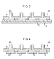
line 2A-2A. - FIG. 3 is a sectional view of a partially sawn wafer held against the vacuum fixture of Figure 2 prior to grinding the back side of the wafer.
- FIG. 4 is a sectional view of a partially sawn wafer held against the vacuum fixture of Figure 2 after grinding the back side of the wafer.
- FIG. 5 is a schematic top view of a vacuum fixture according to a second embodiment of the present invention.
- FIG. 5A is a sectional view of the fixture of Figure 5 taken alone
line 5A-5A. - FIG. 6 is a sectional view of a wafer held against the vacuum fixture of the embodiment of Figure 5 prior to the saw operation.
- FIG. 7 is a sectional view of a wafer held against the vacuum fixture of the embodiment of Figure 5 after the saw operation.
- Figures 1A and 1B show a
silicon wafer 22 on which micromechanical devices, such as digital micromirrors are fabricated. However, it should be understood that this invention is applicable to other substrates and devices.Saw kerfs 24 are made onwafer 22 along scribe marks or streets between the individual devices prior to undercutting the mirrors on the devices. Although the devices shown in figures 1A and 1B are substantially enlarged for illustration purposes such that each figure only shows four rows of devices, each wafer would typically have a substantially larger number of rows. When other micromechanical devices, such as accelerometers or motors, are being fabricated, thepartial saw kerfs 24 should be made prior to any fabrication step that makes the devices too fragile to survive cleaning the dicing debris from the device. After the dicing debris has been washed off, the mirrors are undercut. After the undercutting is completed, the mirrors are fragile and cannot be exposed to many manufacturing processes. Fabrication of the devices, including removal of the sacrificial layer and testing may be completed in wafer form. - Figure 2 shows a
vacuum fixture 26 according to one embodiment of the present invention. Thefixture 26 may be stainless steel, ceramic, quartz, or any other material capable of being machined or formed to the necessary tolerances. Thefixture 26 is machined to have a plurality of headspaces such asheadspace 28 above the devices on the wafer. for example, if micromirror devices are being manufactured theheadspace 28 above the mirrors will help prevent contact with the mirrors. Theheadspaces 28 above each device are connected to a plurality ofvacuum ports 30 to allow theheadspaces 28 to be evacuated. Thefixture 26 includes separatingmembers - When all process steps necessary to complete the devices on the wafer have been completed, the partially
sawn wafer 22 is fitted to avacuum fixture 26 as shown in Figure 3.Headspaces 28 are then evacuated throughvacuum ports 30 and the backside of thewafer 22 is ground down to the partial saw kerfs in order to separate the devices. The operation of grinding the backside of the wafer also provides better thermal management on the completed device. An alternative technique to grinding the backside of the wafer would be to saw the wafers from the backside through to thesaw kerfs 24 on the front side. Another alternative would be to use a tool designed to break the wafers. For certain of these alternative techniques, thefixture 26 may need to be flexible to allow some of the wafer breaking equipment to operate. - Figure 4 shows the completed devices after the devices on the wafer have been separated. Each device is held by the vacuum against the
fixture 26 such that the combination of the devices andfixture 26 may be washed to remove any debris from the separation operation. After washing, the vacuum holding the devices to thefixture 26 is removed to allow thedevice 32 to be removed from thefixture 26. The completed devices are then ready for packaging and any processing further necessary. - An alternate embodiment of the process of this invention does not require the scribe marks or streets to be partially sawn before completion of the devices. According to the alternate embodiment, shown in Figure 5, the
fixture 36 has a plurality ofmachined passages 38 designed to align with the scribe streets of the wafer. Then, as shown in Figure 6, after thewafer 34 is completely fabricated and all wafer level processing steps, including testing, are completed,wafer 34 is mounted tofixture 36 by drawing a vacuum on the headspace throughvacuum ports 40. - The devices on
wafer 34 are separated by a backside sawing operation. As shown in Figure 7, each sawkerf 42 is aligned with apassage 38. As in the prior embodiment the wafer and fixture can now be washed to remove any dicing debris created by the sawing operation. The vacuum is then removed allowing the plurality of completeddevices 44 to be removed from thefixture 36. - Thus, although there has been described to this point a particular embodiment for a method of micromechanical device fabrication in which fragile micromechanical structures are protected from debris during dicing, it is not intended that such specific references be considered as limitations upon the scope of this invention except in-so-far as set forth in the following claims. Furthermore, having described the invention in connection with certain specific embodiments thereof, it is to be understood that further modifications may now suggest themselves to those skilled in the art, it is intended to cover all such modifications as fall within the scope of the appended claims.
Claims (12)
- A fixture for protecting a wafer (22; 34) comprised of at least two micromechanical devices, each micromechanical device comprised of at least one fragile portion, the fixture (26) comprising:a surface for contacting the wafer (22; 34), the surface comprised of a plurality of recessed regions for preventing contact between the surface and the wafer (22; 34) such that when the surface of the fixture (26; 36) is in contact with the wafer (22; 34), each recessed region of the surface forms a headspace (28) above the fragile portion of one of the micromechnical devices;at least one vacuum port (30; 40) connected to the headspaces (28) to allow evacuation of the headspaces (28); andthe surface of the fixture (26; 36) forming a seal around each micromechanical device, thereby allowing each headspace (28) to be evacuated through the vacuum port (30; 40) connected to the headspace (28).
- The fixture of claim 1, the fixture (26; 36) comprised of a material selected from the group consisting of stainless steel, ceramic and quartz.
- The fixture of claim 1 or claim 2, wherein the fixture (26; 36) is rigid.
- The fixture of claim 1, claim 2 or claim 3 and further comprising passages (38) in the surface of the fixture (36), the passages (38) allowing a saw blade to separate the micromechanical devices from the wafer (34) without contacting the fixture (36).
- The fixture of claim 1 wherein the vacuum port is comprised of a separate vacuum port connected to each headspace (28).
- The fixture of claim 1 wherein the vacuum port is comprised of one vacuum port connected to all headspaces (28).
- A method of processing a wafer (22; 34) containing one or more micromechanical devices, said method comprising:placing a protective fixture (26; 36) over and in contact with a first side of said wafer (22; 34), said protective fixture (26; 36) defining a headspace (28) above each device;evacuating said headspace (28) to create a vacuum;grinding the side of said wafer (22; 34) opposite said first side to separate said devices; andremoving said vacuum to release said devices from said fixture (26; 36).
- The method of claim 7 further comprising the step of partially sawing between said devices on said first side prior to placing said wafer (22) in said fixture.
- The method of claim 7 or claim 8 wherein said protective fixture (26; 36) is fabricated of a material selected from the group consisting of stainless steel, ceramic, and quartz.
- The method of claim 7 or claim 8 wherein said protective fixture (26; 36) is a flexible protective fixture.
- The method of any of claims 7 7 to 10 further comprising the step of cleaning debris created by said grinding step from said devices and said protective fixture (26; 36).
- A method of processing a wafer (22; 34) containing one or more micromechanical devices, said method comprising:placing a flexible protective fixture (26; 36) over and in contact with said wafer (22; 34), said protective fixture (26; 36) defining a headspace (28) above each device;evacuating said headspace (28) to create a vacuum;breaking said wafer (22; 34) to separate said devices; andremoving said vacuum to release said devices from said fixture (26; 36).
Applications Claiming Priority (2)
| Application Number | Priority Date | Filing Date | Title |
|---|---|---|---|
| US08/082,183 US5445559A (en) | 1993-06-24 | 1993-06-24 | Wafer-like processing after sawing DMDs |
| US82183 | 1993-06-24 |
Publications (3)
| Publication Number | Publication Date |
|---|---|
| EP0657759A2 EP0657759A2 (en) | 1995-06-14 |
| EP0657759A3 EP0657759A3 (en) | 1995-08-09 |
| EP0657759B1 true EP0657759B1 (en) | 2001-12-05 |
Family
ID=22169571
Family Applications (1)
| Application Number | Title | Priority Date | Filing Date |
|---|---|---|---|
| EP19940109280 Expired - Lifetime EP0657759B1 (en) | 1993-06-24 | 1994-06-16 | Wafer-like processing after sawing DMDs |
Country Status (8)
| Country | Link |
|---|---|
| US (2) | US5445559A (en) |
| EP (1) | EP0657759B1 (en) |
| JP (1) | JPH07153823A (en) |
| KR (1) | KR100276996B1 (en) |
| CN (1) | CN1054210C (en) |
| CA (1) | CA2126111A1 (en) |
| DE (1) | DE69429324T2 (en) |
| TW (1) | TW258828B (en) |
Families Citing this family (94)
| Publication number | Priority date | Publication date | Assignee | Title |
|---|---|---|---|---|
| US6219015B1 (en) | 1992-04-28 | 2001-04-17 | The Board Of Directors Of The Leland Stanford, Junior University | Method and apparatus for using an array of grating light valves to produce multicolor optical images |
| US5597767A (en) * | 1995-01-06 | 1997-01-28 | Texas Instruments Incorporated | Separation of wafer into die with wafer-level processing |
| US5841579A (en) | 1995-06-07 | 1998-11-24 | Silicon Light Machines | Flat diffraction grating light valve |
| US6969635B2 (en) * | 2000-12-07 | 2005-11-29 | Reflectivity, Inc. | Methods for depositing, releasing and packaging micro-electromechanical devices on wafer substrates |
| US5915370A (en) * | 1996-03-13 | 1999-06-29 | Micron Technology, Inc. | Saw for segmenting a semiconductor wafer |
| JP3663728B2 (en) * | 1996-03-28 | 2005-06-22 | 信越半導体株式会社 | Thin plate polishing machine |
| US5872046A (en) * | 1996-04-10 | 1999-02-16 | Texas Instruments Incorporated | Method of cleaning wafer after partial saw |
| US6225191B1 (en) * | 1996-04-12 | 2001-05-01 | Lucent Technologies Inc. | Process for the manufacture of optical integrated circuits |
| US6686291B1 (en) | 1996-05-24 | 2004-02-03 | Texas Instruments Incorporated | Undercut process with isotropic plasma etching at package level |
| US5803797A (en) * | 1996-11-26 | 1998-09-08 | Micron Technology, Inc. | Method and apparatus to hold intergrated circuit chips onto a chuck and to simultaneously remove multiple intergrated circuit chips from a cutting chuck |
| US5809987A (en) | 1996-11-26 | 1998-09-22 | Micron Technology,Inc. | Apparatus for reducing damage to wafer cutting blades during wafer dicing |
| US5982553A (en) | 1997-03-20 | 1999-11-09 | Silicon Light Machines | Display device incorporating one-dimensional grating light-valve array |
| US5817569A (en) * | 1997-05-08 | 1998-10-06 | Texas Instruments Incorporated | Method of reducing wafer particles after partial saw |
| US6088102A (en) | 1997-10-31 | 2000-07-11 | Silicon Light Machines | Display apparatus including grating light-valve array and interferometric optical system |
| US6187654B1 (en) | 1998-03-13 | 2001-02-13 | Intercon Tools, Inc. | Techniques for maintaining alignment of cut dies during substrate dicing |
| US6319075B1 (en) * | 1998-04-17 | 2001-11-20 | Fci Americas Technology, Inc. | Power connector |
| US7314377B2 (en) | 1998-04-17 | 2008-01-01 | Fci Americas Technology, Inc. | Electrical power connector |
| US20020098743A1 (en) * | 1998-04-17 | 2002-07-25 | Schell Mark S. | Power connector |
| US6271808B1 (en) | 1998-06-05 | 2001-08-07 | Silicon Light Machines | Stereo head mounted display using a single display device |
| US6101036A (en) | 1998-06-23 | 2000-08-08 | Silicon Light Machines | Embossed diffraction grating alone and in combination with changeable image display |
| US6130770A (en) | 1998-06-23 | 2000-10-10 | Silicon Light Machines | Electron gun activated grating light valve |
| US6215579B1 (en) | 1998-06-24 | 2001-04-10 | Silicon Light Machines | Method and apparatus for modulating an incident light beam for forming a two-dimensional image |
| US6303986B1 (en) | 1998-07-29 | 2001-10-16 | Silicon Light Machines | Method of and apparatus for sealing an hermetic lid to a semiconductor die |
| JP3516592B2 (en) * | 1998-08-18 | 2004-04-05 | 沖電気工業株式会社 | Semiconductor device and manufacturing method thereof |
| JP3485816B2 (en) * | 1998-12-09 | 2004-01-13 | 太陽誘電株式会社 | Dicing equipment |
| JP4388640B2 (en) * | 1999-09-10 | 2009-12-24 | 株式会社ディスコ | CSP substrate holding member and CSP substrate table on which the CSP substrate holding member is placed |
| US6635512B1 (en) * | 1999-11-04 | 2003-10-21 | Rohm Co., Ltd. | Method of producing a semiconductor device by dividing a semiconductor wafer into separate pieces of semiconductor chips |
| US6521477B1 (en) | 2000-02-02 | 2003-02-18 | Raytheon Company | Vacuum package fabrication of integrated circuit components |
| US6479320B1 (en) * | 2000-02-02 | 2002-11-12 | Raytheon Company | Vacuum package fabrication of microelectromechanical system devices with integrated circuit components |
| US6387778B1 (en) | 2000-02-11 | 2002-05-14 | Seagate Technology Llc | Breakable tethers for microelectromechanical system devices utilizing reactive ion etching lag |
| US6690014B1 (en) | 2000-04-25 | 2004-02-10 | Raytheon Company | Microbolometer and method for forming |
| US6346030B1 (en) * | 2000-05-09 | 2002-02-12 | Sandia Corporation | Microdevice having interior cavity with high aspect ratio surface features and associated methods of manufacture and use |
| KR100332967B1 (en) * | 2000-05-10 | 2002-04-19 | 윤종용 | Method for manufacturing digital micro-mirror device(DMD) package |
| US6425971B1 (en) | 2000-05-10 | 2002-07-30 | Silverbrook Research Pty Ltd | Method of fabricating devices incorporating microelectromechanical systems using UV curable tapes |
| TWI228780B (en) * | 2000-05-11 | 2005-03-01 | Disco Corp | Semiconductor wafer dividing method |
| US6335224B1 (en) | 2000-05-16 | 2002-01-01 | Sandia Corporation | Protection of microelectronic devices during packaging |
| DE60032521T2 (en) * | 2000-05-24 | 2007-11-22 | Silverbrook Research Pty. Ltd., Balmain | METHOD FOR PRODUCING MICROELECTROMECHANICAL DEVICES CONTAINING COMPONENTS BY USING AT LEAST ONE UV-HARDENABLE BAND |
| KR100370398B1 (en) * | 2000-06-22 | 2003-01-30 | 삼성전자 주식회사 | Method for surface mountable chip scale packaging of electronic and MEMS devices |
| US6707591B2 (en) | 2001-04-10 | 2004-03-16 | Silicon Light Machines | Angled illumination for a single order light modulator based projection system |
| US6777681B1 (en) | 2001-04-25 | 2004-08-17 | Raytheon Company | Infrared detector with amorphous silicon detector elements, and a method of making it |
| US6982184B2 (en) * | 2001-05-02 | 2006-01-03 | Silverbrook Research Pty Ltd | Method of fabricating MEMS devices on a silicon wafer |
| US6747781B2 (en) | 2001-06-25 | 2004-06-08 | Silicon Light Machines, Inc. | Method, apparatus, and diffuser for reducing laser speckle |
| US6782205B2 (en) | 2001-06-25 | 2004-08-24 | Silicon Light Machines | Method and apparatus for dynamic equalization in wavelength division multiplexing |
| US6829092B2 (en) | 2001-08-15 | 2004-12-07 | Silicon Light Machines, Inc. | Blazed grating light valve |
| JP4309084B2 (en) * | 2001-11-26 | 2009-08-05 | アピックヤマダ株式会社 | Dicing machine |
| US6800238B1 (en) | 2002-01-15 | 2004-10-05 | Silicon Light Machines, Inc. | Method for domain patterning in low coercive field ferroelectrics |
| US7018268B2 (en) * | 2002-04-09 | 2006-03-28 | Strasbaugh | Protection of work piece during surface processing |
| US6728023B1 (en) | 2002-05-28 | 2004-04-27 | Silicon Light Machines | Optical device arrays with optimized image resolution |
| US6767751B2 (en) | 2002-05-28 | 2004-07-27 | Silicon Light Machines, Inc. | Integrated driver process flow |
| US6822797B1 (en) | 2002-05-31 | 2004-11-23 | Silicon Light Machines, Inc. | Light modulator structure for producing high-contrast operation using zero-order light |
| US6829258B1 (en) | 2002-06-26 | 2004-12-07 | Silicon Light Machines, Inc. | Rapidly tunable external cavity laser |
| US6813059B2 (en) | 2002-06-28 | 2004-11-02 | Silicon Light Machines, Inc. | Reduced formation of asperities in contact micro-structures |
| JP2004062938A (en) * | 2002-07-25 | 2004-02-26 | Pioneer Electronic Corp | Spherical aberration correcting device and spherical aberration correcting method |
| US20040036378A1 (en) * | 2002-08-20 | 2004-02-26 | Rodgers Murray Steven | Dust cover for MEM components |
| US6875257B2 (en) * | 2002-08-20 | 2005-04-05 | Memx, Inc. | Particle filter for microelectromechanical systems |
| US6700173B1 (en) | 2002-08-20 | 2004-03-02 | Memx, Inc. | Electrically isolated support for overlying MEM structure |
| US6801354B1 (en) | 2002-08-20 | 2004-10-05 | Silicon Light Machines, Inc. | 2-D diffraction grating for substantially eliminating polarization dependent losses |
| US6703675B1 (en) | 2002-08-20 | 2004-03-09 | Memx, Inc. | Particle filter for partially enclosed microelectromechanical systems |
| US6712480B1 (en) | 2002-09-27 | 2004-03-30 | Silicon Light Machines | Controlled curvature of stressed micro-structures |
| KR100748145B1 (en) | 2002-11-21 | 2007-08-09 | 실버브룩 리서치 피티와이 리미티드 | Method of Fabricating Devices Incorporating Microelectromechanical Systems Using at Least One UV Curable Tape |
| JP2004221187A (en) * | 2003-01-10 | 2004-08-05 | Toshiba Corp | Manufacturing apparatus and method of semiconductor device |
| US20040147169A1 (en) * | 2003-01-28 | 2004-07-29 | Allison Jeffrey W. | Power connector with safety feature |
| US6806997B1 (en) | 2003-02-28 | 2004-10-19 | Silicon Light Machines, Inc. | Patterned diffractive light modulator ribbon for PDL reduction |
| US6829077B1 (en) | 2003-02-28 | 2004-12-07 | Silicon Light Machines, Inc. | Diffractive light modulator with dynamically rotatable diffraction plane |
| JP4566626B2 (en) * | 2004-06-09 | 2010-10-20 | 株式会社石川製作所 | Semiconductor substrate cutting method and semiconductor chip selective transfer method |
| US7521363B2 (en) | 2004-08-09 | 2009-04-21 | Analog Devices, Inc. | MEMS device with non-standard profile |
| US7416984B2 (en) * | 2004-08-09 | 2008-08-26 | Analog Devices, Inc. | Method of producing a MEMS device |
| US6994608B1 (en) * | 2004-11-12 | 2006-02-07 | Hitachi Global Storage Technologies Netherlands, B.V. | Methods of manufacturing sliders |
| US7109055B2 (en) * | 2005-01-20 | 2006-09-19 | Freescale Semiconductor, Inc. | Methods and apparatus having wafer level chip scale package for sensing elements |
| JP2007095780A (en) * | 2005-09-27 | 2007-04-12 | Oki Electric Ind Co Ltd | Tool and method for manufacturing semiconductor device |
| TW200717519A (en) * | 2005-10-28 | 2007-05-01 | Univ Nat Chiao Tung | Asynchronous first-in-first-out cell |
| US7376215B2 (en) * | 2005-12-27 | 2008-05-20 | Honeywell International Inc. | Measurement of ash composition using scanning high voltage X-ray sensor |
| US7462831B2 (en) * | 2006-01-26 | 2008-12-09 | L-3 Communications Corporation | Systems and methods for bonding |
| US7655909B2 (en) * | 2006-01-26 | 2010-02-02 | L-3 Communications Corporation | Infrared detector elements and methods of forming same |
| US7459686B2 (en) * | 2006-01-26 | 2008-12-02 | L-3 Communications Corporation | Systems and methods for integrating focal plane arrays |
| GB2434913A (en) * | 2006-02-02 | 2007-08-08 | Xsil Technology Ltd | Support for wafer singulation |
| WO2007114331A1 (en) * | 2006-04-04 | 2007-10-11 | Miraial Co., Ltd. | Thin plate container |
| JP2007281053A (en) * | 2006-04-04 | 2007-10-25 | Miraial Kk | Thin plate housing container |
| US7748839B2 (en) * | 2006-05-09 | 2010-07-06 | Lexmark International, Inc. | Handheld printing with reference indicia |
| US7632698B2 (en) | 2006-05-16 | 2009-12-15 | Freescale Semiconductor, Inc. | Integrated circuit encapsulation and method therefor |
| DE102006026467B4 (en) * | 2006-06-07 | 2018-06-28 | Texas Instruments Deutschland Gmbh | Device for grinding a wafer |
| US7718965B1 (en) | 2006-08-03 | 2010-05-18 | L-3 Communications Corporation | Microbolometer infrared detector elements and methods for forming same |
| US8153980B1 (en) | 2006-11-30 | 2012-04-10 | L-3 Communications Corp. | Color correction for radiation detectors |
| US20090061597A1 (en) * | 2007-08-30 | 2009-03-05 | Kavlico Corporation | Singulator method and apparatus |
| US7964106B2 (en) | 2008-05-30 | 2011-06-21 | Unimicron Technology Corp. | Method for fabricating a packaging substrate |
| US8323049B2 (en) * | 2009-01-30 | 2012-12-04 | Fci Americas Technology Llc | Electrical connector having power contacts |
| USD619099S1 (en) | 2009-01-30 | 2010-07-06 | Fci Americas Technology, Inc. | Electrical connector |
| JP5571331B2 (en) * | 2009-07-07 | 2014-08-13 | 株式会社ディスコ | Cutting equipment |
| CN102447017B (en) * | 2010-10-13 | 2014-10-15 | 展晶科技(深圳)有限公司 | LED (Light Emitting Diode) waterproof jig and LED cutting method |
| US8765514B1 (en) | 2010-11-12 | 2014-07-01 | L-3 Communications Corp. | Transitioned film growth for conductive semiconductor materials |
| CN106415814B (en) * | 2014-05-03 | 2019-10-11 | 株式会社半导体能源研究所 | Film-like members support equipment |
| JP2017054956A (en) * | 2015-09-10 | 2017-03-16 | 株式会社ディスコ | Support tool for workpiece |
| JP2017038072A (en) * | 2016-09-29 | 2017-02-16 | 三星ダイヤモンド工業株式会社 | Conveyance head of fragile material substrate |
| JP6970554B2 (en) * | 2017-08-21 | 2021-11-24 | 株式会社ディスコ | Processing method |
Family Cites Families (15)
| Publication number | Priority date | Publication date | Assignee | Title |
|---|---|---|---|---|
| US3809050A (en) * | 1971-01-13 | 1974-05-07 | Cogar Corp | Mounting block for semiconductor wafers |
| US3811182A (en) * | 1972-03-31 | 1974-05-21 | Ibm | Object handling fixture, system, and process |
| US3994101A (en) * | 1973-01-03 | 1976-11-30 | Coburn Optical Industries, Inc. | Vacuum chuck with sealable cavity |
| US3971170A (en) * | 1973-01-03 | 1976-07-27 | Coburn Optical Industries, Inc. | Vaccum chuck with sealable cavity |
| US3976288A (en) * | 1975-11-24 | 1976-08-24 | Ibm Corporation | Semiconductor wafer dicing fixture |
| US4138304A (en) * | 1977-11-03 | 1979-02-06 | General Electric Company | Wafer sawing technique |
| US4213698A (en) * | 1978-12-01 | 1980-07-22 | Bell Telephone Laboratories, Incorporated | Apparatus and method for holding and planarizing thin workpieces |
| US4184292A (en) * | 1978-03-24 | 1980-01-22 | Revlon, Inc. | Vacuum chuck |
| DE3463227D1 (en) * | 1984-08-03 | 1987-05-27 | Loh Kg Optikmaschf | Supporting device for vulnerable objects, in particular optical lenses and other optical elements |
| US5061049A (en) * | 1984-08-31 | 1991-10-29 | Texas Instruments Incorporated | Spatial light modulator and method |
| US5291692A (en) * | 1989-09-14 | 1994-03-08 | Olympus Optical Company Limited | Polishing work holder |
| ES2096118T3 (en) * | 1990-01-31 | 1997-03-01 | Bando Kiko Co | MACHINE TO WORK A GLASS PLATE. |
| US5029418A (en) * | 1990-03-05 | 1991-07-09 | Eastman Kodak Company | Sawing method for substrate cutting operations |
| JPH04276645A (en) * | 1991-03-04 | 1992-10-01 | Toshiba Corp | Dicing method of compound semiconductor wafer |
| US5393706A (en) * | 1993-01-07 | 1995-02-28 | Texas Instruments Incorporated | Integrated partial sawing process |
-
1993
- 1993-06-24 US US08/082,183 patent/US5445559A/en not_active Expired - Fee Related
-
1994
- 1994-06-16 DE DE1994629324 patent/DE69429324T2/en not_active Expired - Fee Related
- 1994-06-16 EP EP19940109280 patent/EP0657759B1/en not_active Expired - Lifetime
- 1994-06-17 CA CA 2126111 patent/CA2126111A1/en not_active Abandoned
- 1994-06-23 KR KR1019940014413A patent/KR100276996B1/en not_active IP Right Cessation
- 1994-06-23 JP JP14187194A patent/JPH07153823A/en not_active Ceased
- 1994-06-24 CN CN94107015A patent/CN1054210C/en not_active Expired - Fee Related
- 1994-08-29 TW TW83107896A patent/TW258828B/zh active
-
1995
- 1995-05-23 US US08/448,205 patent/US5605489A/en not_active Expired - Lifetime
Also Published As
| Publication number | Publication date |
|---|---|
| CA2126111A1 (en) | 1994-12-25 |
| CN1104341A (en) | 1995-06-28 |
| CN1054210C (en) | 2000-07-05 |
| US5605489A (en) | 1997-02-25 |
| KR100276996B1 (en) | 2001-02-01 |
| DE69429324D1 (en) | 2002-01-17 |
| KR950001989A (en) | 1995-01-04 |
| EP0657759A3 (en) | 1995-08-09 |
| JPH07153823A (en) | 1995-06-16 |
| EP0657759A2 (en) | 1995-06-14 |
| TW258828B (en) | 1995-10-01 |
| DE69429324T2 (en) | 2002-08-08 |
| US5445559A (en) | 1995-08-29 |
Similar Documents
| Publication | Publication Date | Title |
|---|---|---|
| EP0657759B1 (en) | Wafer-like processing after sawing DMDs | |
| US5622900A (en) | Wafer-like processing after sawing DMDs | |
| US6465329B1 (en) | Microcircuit die-sawing protector and method | |
| US6642127B2 (en) | Method for dicing a semiconductor wafer | |
| US5389182A (en) | Use of a saw frame with tape as a substrate carrier for wafer level backend processing | |
| US5527744A (en) | Wafer method for breaking a semiconductor | |
| US7250353B2 (en) | Method and system of releasing a MEMS structure | |
| US6521513B1 (en) | Silicon wafer configuration and method for forming same | |
| US5710065A (en) | Method and apparatus for breaking and separating dies from a wafer | |
| US6573156B1 (en) | Low defect method for die singulation and for structural support for handling thin film devices | |
| US20020096743A1 (en) | Method and device for protecting micro electromechanical systems structures during dicing of a wafer | |
| US8030180B2 (en) | Method of manufacturing a semiconductor device | |
| US6661080B1 (en) | Structure for backside saw cavity protection | |
| WO2011021981A1 (en) | Method of dicing a wafer | |
| WO2001043169A2 (en) | Methods for separating microcircuit dies from wafers | |
| US20070031989A1 (en) | Separating semiconductor wafers having exposed micromechanical structures into individual chips | |
| KR100284018B1 (en) | Semiconductor Wafer Process | |
| JPH0864558A (en) | Method of manufacturing micro electronic mechanical type device | |
| JP3221394B2 (en) | Dicing method for semiconductor device | |
| KR19980053148A (en) | Wafer cutting method |
Legal Events
| Date | Code | Title | Description |
|---|---|---|---|
| PUAI | Public reference made under article 153(3) epc to a published international application that has entered the european phase |
Free format text: ORIGINAL CODE: 0009012 |
|
| AK | Designated contracting states |
Kind code of ref document: A2 Designated state(s): DE FR GB IT NL |
|
| PUAL | Search report despatched |
Free format text: ORIGINAL CODE: 0009013 |
|
| AK | Designated contracting states |
Kind code of ref document: A3 Designated state(s): DE FR GB IT NL |
|
| 17P | Request for examination filed |
Effective date: 19960131 |
|
| 17Q | First examination report despatched |
Effective date: 19990514 |
|
| GRAG | Despatch of communication of intention to grant |
Free format text: ORIGINAL CODE: EPIDOS AGRA |
|
| RIC1 | Information provided on ipc code assigned before grant |
Free format text: 7G 02B 26/02 A, 7G 02B 26/08 B, 7G 09F 9/37 B, 7B 65G 49/07 B, 7H 01L 21/68 B |
|
| RTI1 | Title (correction) |
Free format text: WAFER-LIKE PROCESSING AFTER SAWING DMDS |
|
| GRAG | Despatch of communication of intention to grant |
Free format text: ORIGINAL CODE: EPIDOS AGRA |
|
| GRAH | Despatch of communication of intention to grant a patent |
Free format text: ORIGINAL CODE: EPIDOS IGRA |
|
| GRAG | Despatch of communication of intention to grant |
Free format text: ORIGINAL CODE: EPIDOS AGRA |
|
| GRAH | Despatch of communication of intention to grant a patent |
Free format text: ORIGINAL CODE: EPIDOS IGRA |
|
| GRAH | Despatch of communication of intention to grant a patent |
Free format text: ORIGINAL CODE: EPIDOS IGRA |
|
| GRAA | (expected) grant |
Free format text: ORIGINAL CODE: 0009210 |
|
| AK | Designated contracting states |
Kind code of ref document: B1 Designated state(s): DE FR GB IT NL |
|
| REG | Reference to a national code |
Ref country code: GB Ref legal event code: IF02 |
|
| REF | Corresponds to: |
Ref document number: 69429324 Country of ref document: DE Date of ref document: 20020117 |
|
| ET | Fr: translation filed | ||
| PLBE | No opposition filed within time limit |
Free format text: ORIGINAL CODE: 0009261 |
|
| STAA | Information on the status of an ep patent application or granted ep patent |
Free format text: STATUS: NO OPPOSITION FILED WITHIN TIME LIMIT |
|
| 26N | No opposition filed | ||
| PGFP | Annual fee paid to national office [announced via postgrant information from national office to epo] |
Ref country code: IT Payment date: 20070627 Year of fee payment: 14 |
|
| PGFP | Annual fee paid to national office [announced via postgrant information from national office to epo] |
Ref country code: DE Payment date: 20080630 Year of fee payment: 15 Ref country code: NL Payment date: 20080530 Year of fee payment: 15 |
|
| PGFP | Annual fee paid to national office [announced via postgrant information from national office to epo] |
Ref country code: GB Payment date: 20080506 Year of fee payment: 15 |
|
| PG25 | Lapsed in a contracting state [announced via postgrant information from national office to epo] |
Ref country code: IT Free format text: LAPSE BECAUSE OF NON-PAYMENT OF DUE FEES Effective date: 20080616 |
|
| GBPC | Gb: european patent ceased through non-payment of renewal fee |
Effective date: 20090616 |
|
| NLV4 | Nl: lapsed or anulled due to non-payment of the annual fee |
Effective date: 20100101 |
|
| REG | Reference to a national code |
Ref country code: FR Ref legal event code: ST Effective date: 20100226 |
|
| PG25 | Lapsed in a contracting state [announced via postgrant information from national office to epo] |
Ref country code: FR Free format text: LAPSE BECAUSE OF NON-PAYMENT OF DUE FEES Effective date: 20090630 |
|
| PGFP | Annual fee paid to national office [announced via postgrant information from national office to epo] |
Ref country code: FR Payment date: 20080424 Year of fee payment: 15 |
|
| PG25 | Lapsed in a contracting state [announced via postgrant information from national office to epo] |
Ref country code: GB Free format text: LAPSE BECAUSE OF NON-PAYMENT OF DUE FEES Effective date: 20090616 |
|
| PG25 | Lapsed in a contracting state [announced via postgrant information from national office to epo] |
Ref country code: DE Free format text: LAPSE BECAUSE OF NON-PAYMENT OF DUE FEES Effective date: 20100101 |
|
| PG25 | Lapsed in a contracting state [announced via postgrant information from national office to epo] |
Ref country code: NL Free format text: LAPSE BECAUSE OF NON-PAYMENT OF DUE FEES Effective date: 20100101 |